

Page 1
HT-CN9900DVW
PRECAUTIONS FOR USING LEAD-FREE SOLDER
CHAPTER 1. GENERAL DESCRIPTION
[1] Safety Precaution For Service Manual.........1-1
[2]
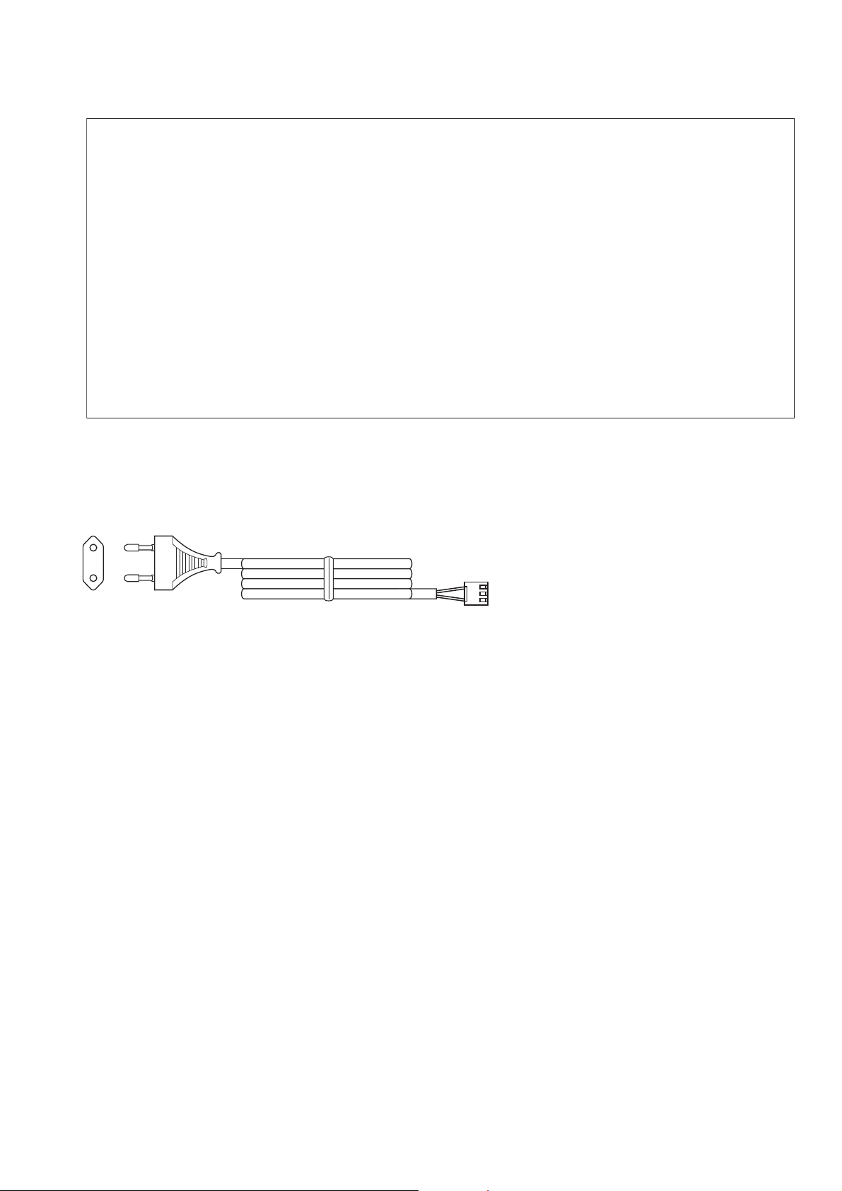
AC Power Supply Cord
..................................1-1
[3] Specifications ...............................................1-2
[4] Names Of Parts............................................1-3
CHAPTER 2. MECHANICAL DESCRIPTION
[1] Disassembly ................................................2-1
CHAPTER 3. FLOWCHART
[1] Troubeshooting ............................................3-1
CHAPTER 4. MAJOR PART DRAWING
[1] Function Table Of IC .................................... 4-1
[2] VFD Display.............................................. 4-10
CHAPTER 5. CIRCUIT DESCRIPTION
[1] Waveforms Of Servo Circuit..........................5-1
[2] Voltage..........................................................5-3
CHAPTER 6. DIAGRAMS
[1] Block Diagram...............................................6-1
CHAPTER 7. CIRCUIT SCHEMATICS AND PARTS
LAYOUT
[1] Notes On Schematic Diagram ......................7-1
[2] Type Of Transistor And LED .........................7-1
[3] Schematic Diagram ......................................7-2
[4] Charts Of Connecting Wires.........................7-5
[5] Wiring Side Of PWB .....................................7-6
PARTS GUIDE
HT-CN9900DVW
!
SERVICE MANUAL
No. S7119HTC990DZ
HOME THEATER WITH DVD
MODEL
Singapore, Malaysia, Indonesia, Philippines and India]
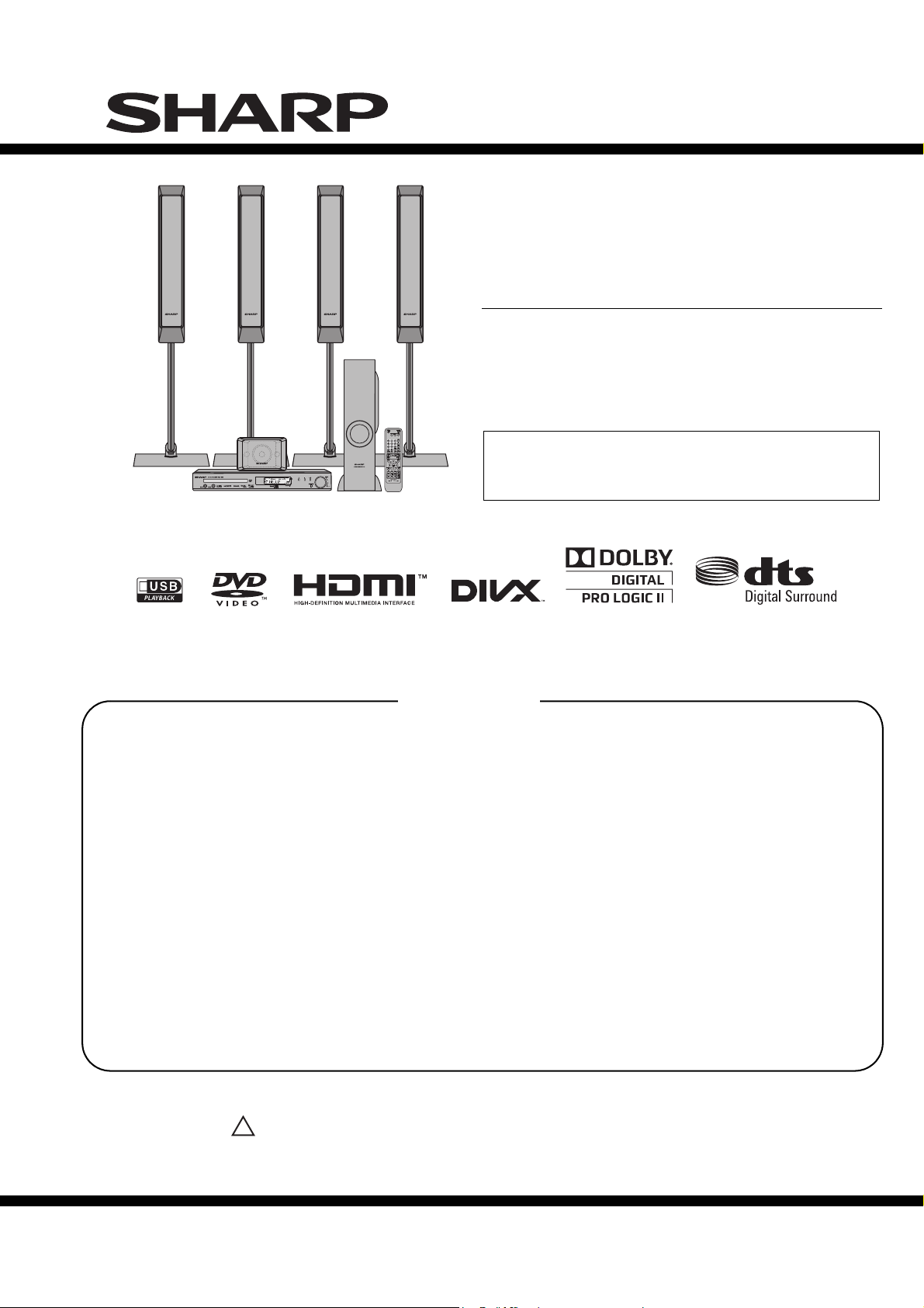
HT-CN9900DVW Home Theater with DVD consisting of
HT-CN9900DVW (main unit), CP-CN9900F (front speakers),
CP-CN9900C (centre speaker), CP-CN9900R (surround
speakers) and CP-CN9900W (subwoofer).
• In the interests of user-safety (Required by safety
regulations in some countries) the set should be restored to
its original condition and only parts identical to those
specified be used.
CONTENTS
HT-CN9900DVW
[For Jordan, Singapore-Export,
Parts marked with " " are important for maintaining the safety of the set. Be sure to replace these parts with
specified ones for maintaining the safety and performance of the set.
SHARP CORPORATION
This document has been published to be used for
after sales service only.
The contents are subject to change without notice.
Page 2
HT-CN9900DVW
PRECAUTIONS FOR USING LEAD-FREE SOLDER
1. Employing lead-free solder
Lead-free wire solder for servicing
Ref No.
Description
Parts No.
"MAIN/AMP, DISPLAY, USB, MIC, SMPS PWB" of this model employs lead-free solder.
The LF symbol indicates lead-free solder, and is attached on the PWB and service manuals. The alphabetical
character following LF shows the type of lead-free solder.
2. Using lead-free wire solder
When fixing the PWB soldered with the lead-free solder, apply lead-free wire solder. Repairing with conventional
lead wire solder may cause damage or accident due to cracks.
As the melting point of lead-free solder (Sn-Ag-Cu) is higher than the lead wire solder by 40 C, we recommend
you to use a dedicated soldering bit, if you are not familiar with how to obtain lead-free wire solder or soldering
bit, contact our service sta
tion or service branch in your area.
3.
Soldering
As the melting point of lead-free solder (Sn-Ag-Cu) is about 220°C which is higher than the conventional lead
solder by 40°C,and as it has poor solder wettability, you may be apt to keep the soldering bit in contact with the
PWB for extended period of time. However, since the land may be peeled of for the maximum heat-resistance
temperature of parts may be exceeded, remove the bit from the PWB as soon as you confirm the steady
soldering condition.
Lead-free solder contains more tin, and the end of the soldering bit may be easily corrected. Make sure to turn
on and off the power of the bit as required. If a different type of solder stays on the tip of the soldering bit, it is
alloyed with lead-free solder. Clean the bit after every use of it.
When the tip of the soldering bit is blackened during use, file it with steel wool or fine sand paper.
Be careful when replacing parts with pola
rity indication on the PWB silk.
Example:
Indicates lead-free solder of tin, silver and copper.
PWB-A 92LPWB8315MANS
PWB-A 92LPWB8316MANS
PWB-A 92LPWB8327MANS
PWB-A 92LPWB8328MANS
PWB-B RUiTZA049AWZZ
MAIN/AMP (A1), DISPLAY (A2), USB (A3), MIC (A4)
[ For Jordan, Singapore-Export ]
MAIN/AMP (A1), DISPLAY (A2), USB (A3), MIC (A4)
[ For Singapore, Malaysia, Indonesia ]
MAIN/AMP (A1), DISPLAY (A2), USB (A3), MIC (A4)
[ For Philippines ]
MAIN/AMP (A1), DISPLAY (A2), USB (A3), MIC (A4)
[ For India ]
SMPS
– 1
i
Page 3
CHAPTER 1. GENERAL DESCRIPTION
This product is classified as a CLASS 1 LASER PRODUCT.
WARNINGS
THE AEL (ACCESSIBLE EMISSION LEVEL) OF LASER POWER OUTPUT FOR THIS MODEL IS SPECIFIED TO
BE LOWER THAN CLASS I REQUIREMENTS. HOWEVER, THE FOLLOWING PRECAUTIONS MUST BE OBSERVED
DURING SERVICING TO PROTECT YOUR EYES AGAINTS EXPOSURE TO THE LASER BEAM.
1- WHEN THE CABINET HAS BEEN REMOVED, THE POWER IS TURNED ON WITHOUT A COMPACT DISC,
AND THE PICKUP IS ON A POSITION OUTER THAN THE LEAD-IN POSITION, THE LASER WILL LIGHT FOR
SEVERAL SECONDS TO DETECT A DISC.
DO NOT LOOK INTO THE PICKUP LENS.
2- THE LASER POWER OUTPUT OF THE PICKUP INSIDE THE UNIT AND REPLACEMENT SERVICE PARTS
HAVE ALREADY BEEN ADJUSTED PRIOR TO SHIPPING.
3- NO ADJUSTMENT TO THE LASER POWER SHOULD BE ATTEMPTED WHEN REPLACING OR SERVICING
THE PICKUP.
4- UNDER NO CIRCUMSTANCES LOOK DIRECTLY INTO THE PICKUP LENS AT ANY TIME.
5- CAUTION - USE OF CONTROLS OR ADJUS
TMENTS, OR PERFORMANCE OF PROCEDURES OTHER THAN
THOSE SPECIFIED HEREIN MAY RESULT IN HAZARDOUS RADIATION EXPOSURE.
QACCEA001AW00
[1] Safety Precaution For Service Manual
HT-CN9900DVW
[2] AC Power Supply Cord
1 – 2
1 – 1
Page 4
HT-CN9900DVW
Main unit
USB
Tuner
DVD player
Subwoofer
CP-CN9900 F/R Speaker
Power source AC 220 - 240 V ~ 50/60 Hz
Power
consumption
Power on: 120 W
Output power Front speaker
(CP-CN9900):
RMS: 200 W (100 W + 100 W)
(10% T.H.D.)
Surround speaker
(CP-CN9900):
RMS: 200 W (100 W + 100 W)
(10% T.H.D.)
Centre speaker
(CP-CN9900):
RMS: 100 W (10% T.H.D.)
Subwoofer:
RMS: 100 W (10% T.H.D.)
Video output
terminals
Video output: RCA type x 1
HDMI output: HDMI x 1
Support 480p/570p/1080p output
formats.
Audio input
terminals
Analogue input: 500 mV/47 k ohms
Microphone 1/2: 1 mV/600 ohms
Audio output
terminals
Speakers: 6 ohms
Subwoofer: 6 ohms
Dimensions
Width: 430 mm (16-15/16")
Height: 65.7 mm (2-19/32")
Depth: 320.3 mm (12-1/2")
Weight 3.4 kg (7.5 lbs.)
USB host
interface
Complies with USB 1.1/2.0 (Full
Speed) Mass Storage Class.
Support Bulk only and CBI protocol.
Support file JPEG
File system
support
Support USB devices with
Microsoft Windows/DOS/FAT 16/
FAT 32.
2 kbyte block length for sector.
Frequency
range
FM: 87.5 - 108 MHz
Other Maximum station can be stored is 40
preset.
Signal system PAL/NTSC colour
Supported disc
types
DVD (with the same region number at
the back of the unit), audio CD, CD-R,
CD-RW, JPEG, DivX
Video signal Horizontal resolution: 500 lines
S/N ratio: 70 dB
Audio signal Frequency
characteristic
s
Linear PCM DVD:
20 Hz to 20 kHz
(sampling rate: 48
kHz)
20 Hz to 20 kHz
(sampling rate: 96
kHz)
CD: 20 Hz to 20 kHz
S/N ratio CD: 94 dB (1 kHz)
Dynamic range Linear PCM DVD:
95 dB
CD: 94 dB
Total harmonic
distortion ratio
0.01% maximum
Type Full range speaker system
6.5 cm (2-1/2") woofer
Maximum input
power
200 W
Rated input
power
100 W
Impedance 6 ohms
Dimensions Width: 154 mm (6-1/16")
Height: 103 mm (4-1/16")
Depth: 84 mm (3-5/16")
Weight 0.5 kg (1.1 lbs.)
Type Subwoofer system
13 cm (5-1/8") subwoofer
Maximum input
power
200 W
Rated input
power
100 W
Impedance 6 ohms
Dimensions Width: 115 mm (4-1/2")
Height: 421 mm (16-9/16")
Depth: 396 mm (15-9/16")
Weight 4.3 kg (9.5 lbs.)
Type Full range speaker system
6.5 cm (2-1/2") woofer
Maximum input
power
200 W
Rated input power 100 W
Impedance 6 ohms
Dimensions Width: 250 mm (9-13/16")
Height: 1030 mm (40-9/16")
Depth: 250 mm (9-13/16")
Weight 1.5 kg (3.3 lbs.)
CP-CN9900 C Speaker
[3] Specifications
1 – 3
1 – 2
Page 5
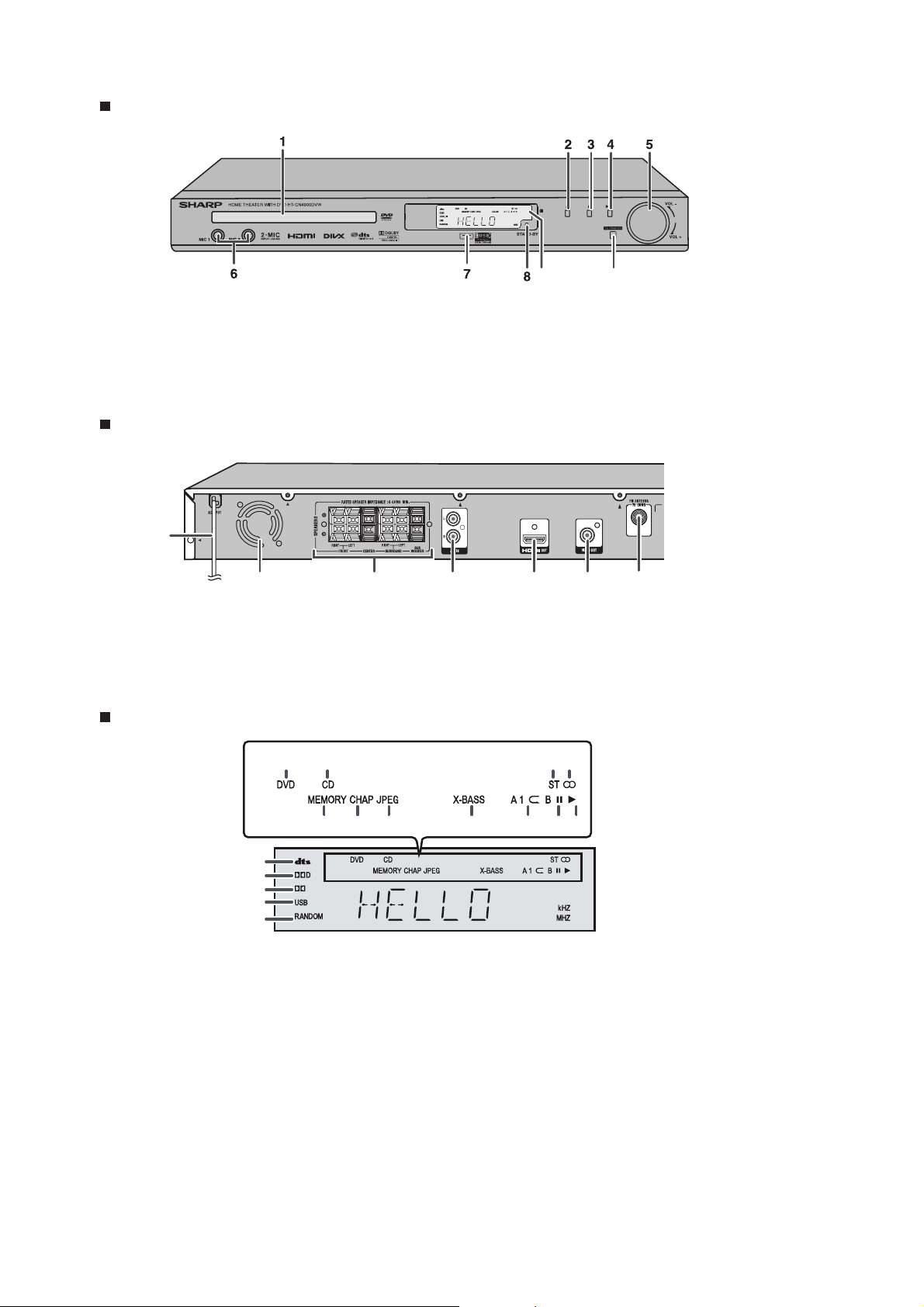
[4] Names Of Parts
1
3 4 65 72
Main unit (front panel)
1. Disc Tray
2. Disc Tray Open/Close Button
3. Stop Button
4. Play/Pause Button
5. Volume Control
Main unit (rear panel)
HT-CN9900DVW
109
6. Microphone Sockets
7. USB Terminal
8. Stand-by Indicator
9. Remote Sensor
10. On/Stand-by Button
1. AC Power Lead
2. Cooling Fan
3. Speaker Terminals
4. Auxiliary Input Sockets
Display
12
13
14
15
16
1. DVD Indicator
2. CD Indicator
3. FM Stereo Mode Indicator
4. FM Stereo Receiving Indicator
5. Memory Indicator
6. Chapter Indicator
7. JPEG Indicator
8. Extra Bass Indicator
1 2
5 6 78 11109
PLII
5. HDMI Socket
6. Video Output Socket
7. FM 75 Ohms Aerial Socket
43
9. Repeat Play Indicator
10. Pause Indicator
11. Play Indicator
12. DTS Indicator
13. Dolby Digital Signal Indicator
14. Dolby Pro-Logic Indictor
15. USB indicator
16. Random Indicator
1 – 4
1 – 3
Page 6
HT-CN9900DVW
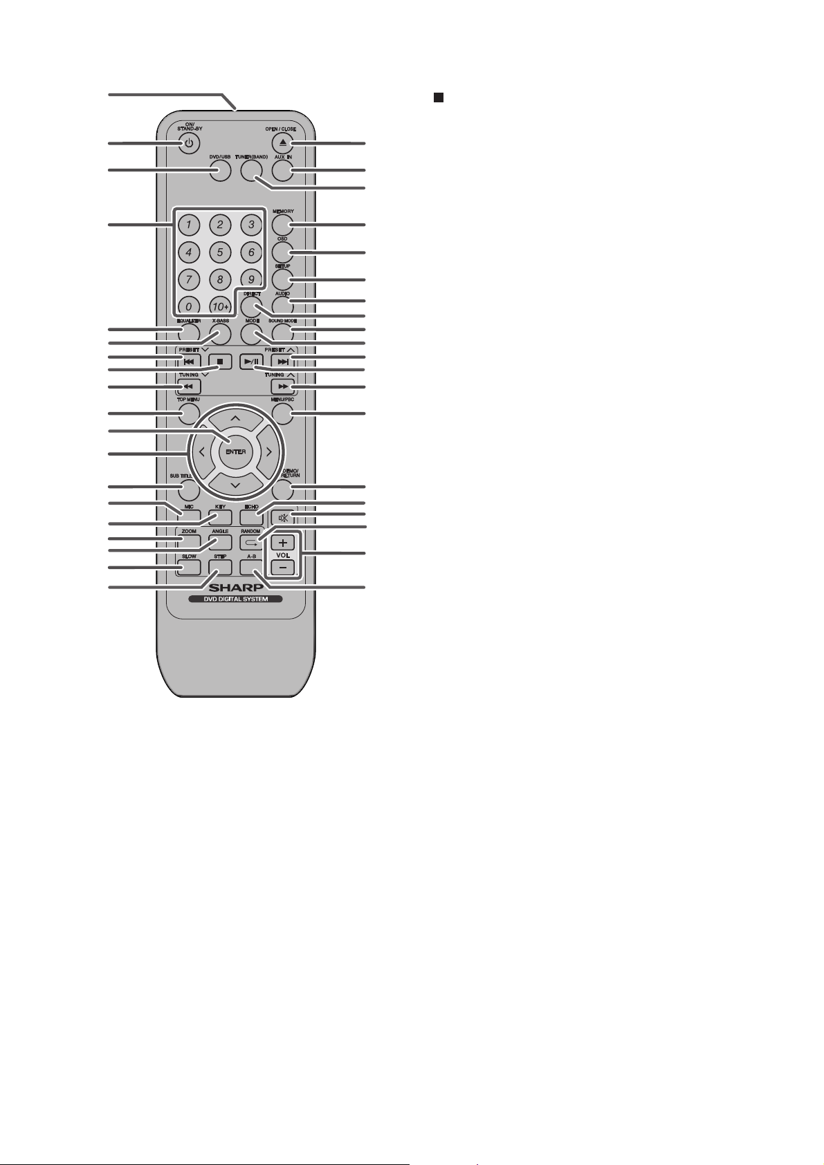
Remote control
1. Remote Control Transmitter
2. On/Stand-by Button
3. DVD/USB Button
4. Numeric Buttons
5. Equaliser Button
6. X-Bass Button
7. Chapter (Track) Skip Down or Preset Down Button
8. Stop Button
9. Fast Reverse or Tuning Down Button
10. Top Menu Button
11. Enter Button
12. Cursor Buttons
13. Subtitle Button
14. Mic Button
15. Key Button
16. Zoom Button
17. Angle Button
18. Slow Button
19. Step Button
20. Disc Tray Open/Close Button
21. AUX IN Button
22. Tuner (Band) Button
23. Memory Button
24. OSD Button
25. Setup Button
26. Audio Button
27. Direct Button
28. Sound Mode Button
29. Mode Button
30. Chapter (Track) Skip Up or Preset Up Button
31. DVD/CD Play and Pause Button
32. Fast Forward or Tuning Up Button
33. Menu/PBC Button
34. Demo/Return Button
35. Echo Button
36. Mute Button
37. Random/Repeat Button
38. Volume Up and Down Buttons
39. A-B Repeat Button
2
1
3
4
5
6
7
8
9
10
11
12
13
14
15
16
17
18
19
20
21
22
23
24
25
26
27
28
29
30
31
32
33
34
35
36
37
38
39
1 – 5
1 – 4
Page 7
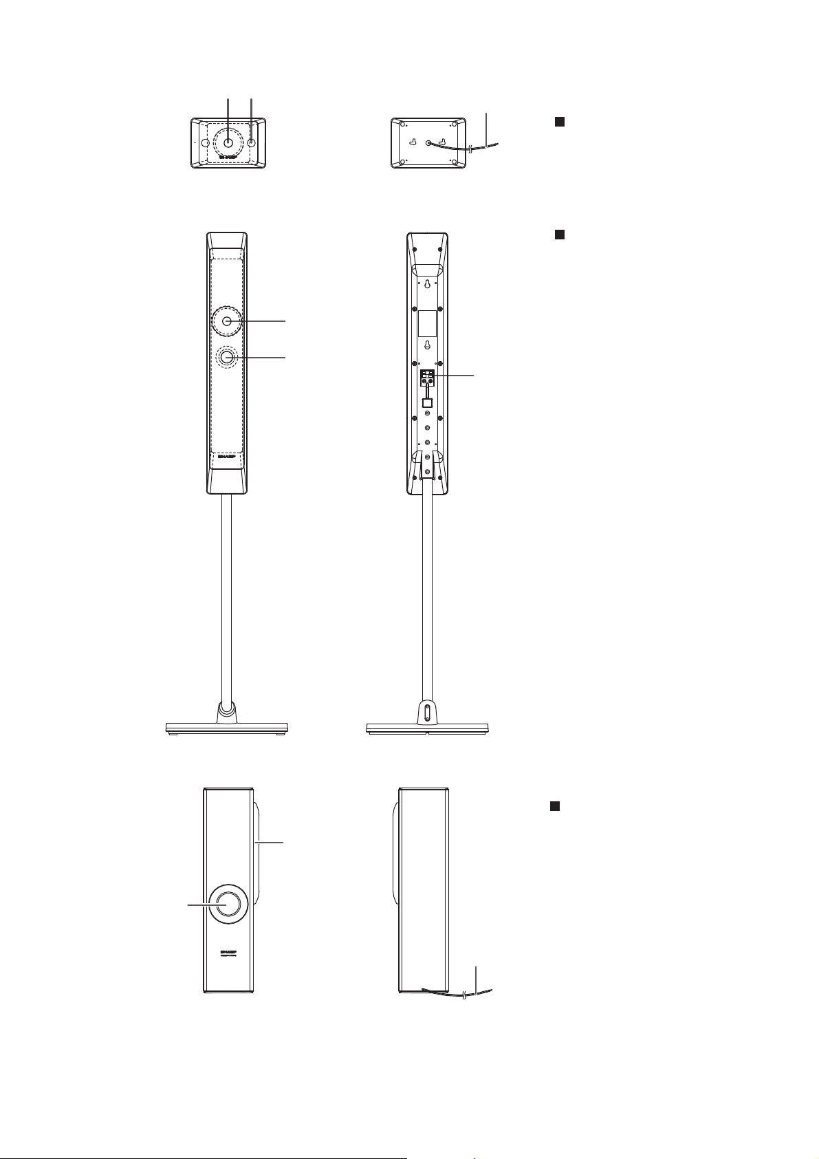
1
2
FRONT VIEW REAR VIEW
1
2
HT-CN9900DVW
3
Center speaker
1. Woofer
2. Bass Reflex Duct
3. Speaker Wire
Front/Surround speakers
1. Woofer
2. Bass Reflex Duct
3. Speaker Terminal
3
FRONT VIEW REAR VIEW
2
1
1 – 6
1 – 5
Subwoofer
1. Bass Reflex Duct
2. Subwoofer
3. Speaker Wire
3
Page 8
HT-CN9900DVW
CD-ES700/CD-ES77CD-ES700/CD-ES77Service ManualCD-ES700/CD-ES77MarketE
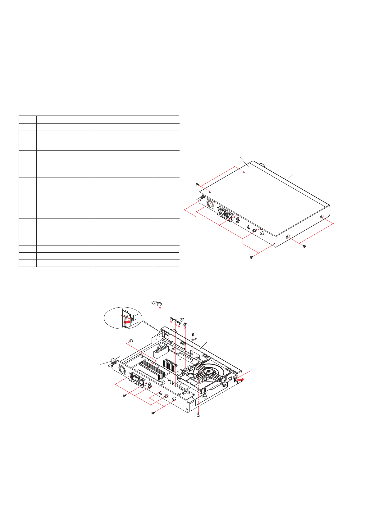
CHAPTER 2. MECHANICAL DESCRIPTION
[1] Disassembly
Caution On Disassembly
Follow the below-mentioned notes when disassembling the unit and reassembling it, to keep it safe and ensure
excellent performance:
1. Take compact disc out of the unit.
2. Be sure to remove the power supply plug from the wall outlet before starting to disassemble the unit.
3. Take off nylon bands or wire holders where they need to be removed when disassembling the unit. After servicing
the unit, be sure to rearrange the leads where they were before disassembling.
STEP REMOVAL PROCEDURE FIGURE
1 Top Cabinet
2 Rear Panel
3 Front Panel Assy
4 Loader Assy with
DVD Mechanism Unit
5 Main/Amp PWB
6 SMPS PW B
7Display PWB
8USB PWB
9Mic PWB
10 DVD Mechanism Unit
1. Screw............
1. Screw............
2. Screw............
3. Socket ..........
1. Screw............
2. Screw............
3. Socket ..........
4. Hook .............
1. Screw............
2. Flat Cable .....
3. Socket ..........
1. Screw............
2. Socket ..........
1. Screw............
1. Knob .............
2. Nut................
3. Washer .........
4. Screw............
1. Screw............
1. Screw............
1. Screw............
(A1)x9 1
(B1)x4 2
(B2)x2
(B3)x2
(C1)x1 2
(C2)x1
(C3)x4
(C4)x2
(D1)x4 3
(D2)x1
(D3)x2
(E1)x3 3
(E2)x2
(F1)x5 3
(G1)x1 4
(G2)x1
(G3)x1
(G4)x3
(H1)x2 4
(J1)x2 4
(K1)x4 5
(A1) x 2
Special Screw
Top Cabinet
(A1) x 5
Special Screw
Front Panel Assy
(A1) x 2
Special Screw
Rear Panel
Hook
(C4) x 1
PULL
(B3) x 1
(B1) x 3
M3 x 8mm
(B3) x 1
(B2) x 2
M3 x 6mm
Figure 2
(C3) x 4
(C2) x 1
Special Screw
Front Panel Assy
(C1) x 1
M3 x 6mm
PULL
Figure 1
Hook
(C4) x 1
2 – 1
Page 9
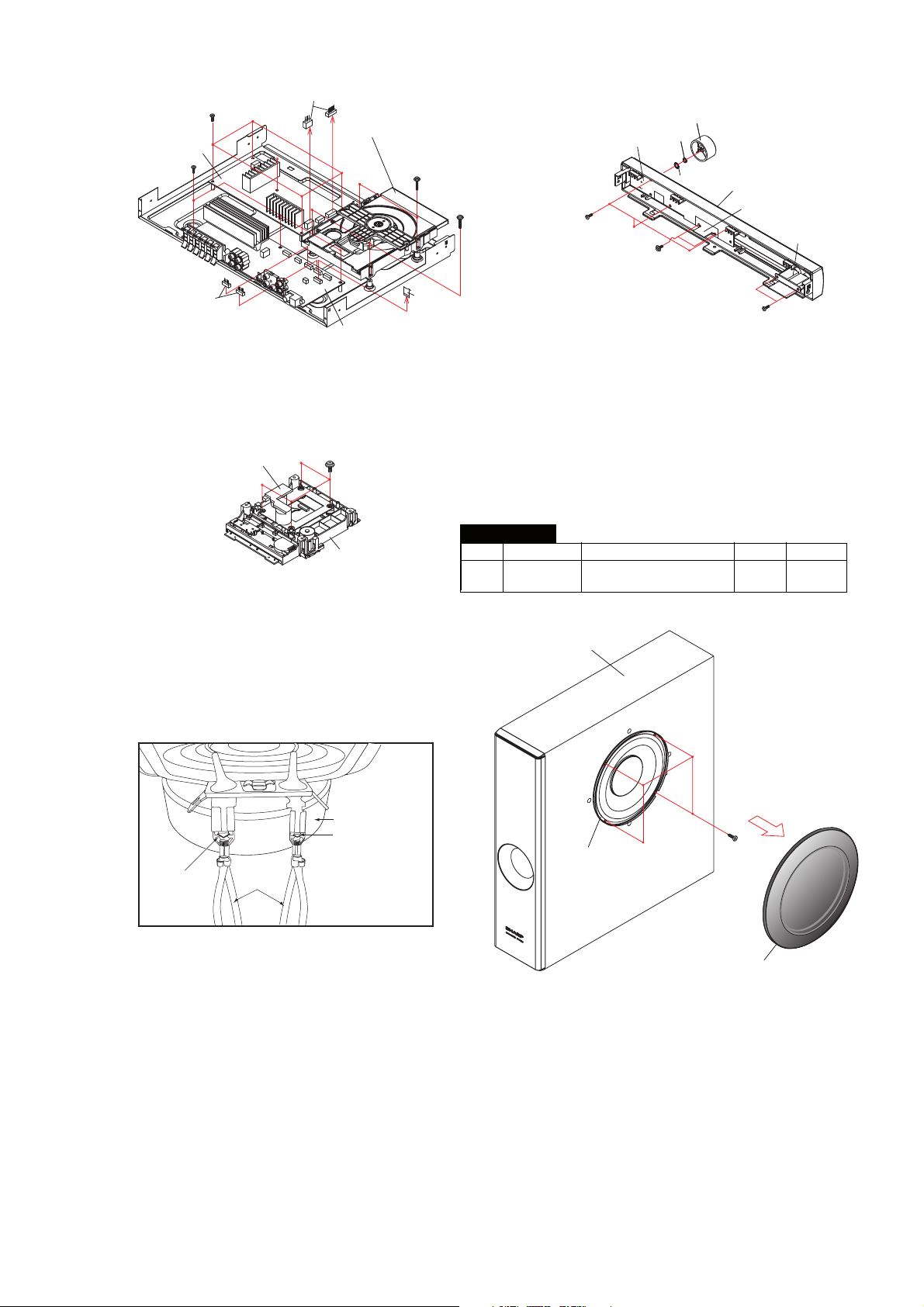
HT-CN9900DVW
Figure 5
Figure 3 Figure 4
CAUTION:
TO REMOVE SPEAKER UNIT, PRESS THESE LOCKING TABS
TO RELEASE SPEAKER WIRES.
SPEAKER UNIT
LOCKING
TAB
LOCKING TAB
SPEAKER
WIRE
(F1) x 5
M3 x 8mm
(J1) x 2
M3 x 8mm
(A2) x 4
M4 x 16mm
(A1) x 1
Net Frame Ass,y
(G4) x 3
M3 x 8mm
Display PWB
(E1) x 3
M3 x 8mm
(E2) x 2
(G1) x 1
(G2) x 1
(G3) x 1
Front Panel Assy
USB PWB
Mic PWB
(D3) x 2
(D2) x 1
Main/Amp PWB
SMPS PWB
Loader Assy with
DVD Mechanism
(D1) x 2
Special Screw
(H1) x 2
Special Screw
(K1) x 4
Special Screw
DVD Mechanism Unit
Loader Assy
Wooden Box Ass’y
Subwoofer
(D1) x 2
Special Screw
Figure 6
STEP REMOVAL PROCEDURE FIGURE
1 Subwoofer
1. Net Frame Ass'y ..............
(A1)x1 6
2. Screw...............................
(A2)x4
Subwoofer
2 – 2
Page 10

HT-CN9900DVW
1. When the CD/DVD does not function
The CD/DVD section may not operate when the objective lens of the optical pickup is dirty. Clean the objective lens,
and check the playback operation. When this section does not operate even after the above step is taken, check the following items.
Remove the cabinet and follow the trouble shooting instructions.
"Track skipping and/or no TOC (Table Of Contents) may be caused by build up of dust other foreign matter on the laser
pickup lens. Before attempting any adjustment make certain that the lens is clean. If not, clean it as mentioned below."
Turn the power off.
Gently clean the lens with a lens cleaning tissue and a small amount of isopropyl alcohol.
Do not touch the lens with the bare hand.
2. When a CD/DVD cannot be played
2.1. Pressing the CD/DVD operation key is accepted, but playback does not occur.
1) Focus error system check
2) Both Video and Audio do not operate normally
Par ts code
1. CD optical pickup Lens cleaner disc UDSKA0004AFZZ
HOW TO USE
CAUTION
Cleaning fluid
Cleaner disc
Using the brush in the cleaner cap, apply 1 or 2 drops of the cleaning fluid to the
brush on the CD cleaner disc which has the mark next to it.
Place the CD cleaner disc onto the CD/DVD disc compartment with the brush side
down, then press the play button.
You will hear music for about 20 seconds and the CD/DVD player will automatically
stop. If it still play continuously, press the stop button.
1.
2.
3.
The CD lens cleaner should be effective for 30-50 operations, however if the brushes
become worn out earlier then please replace the cleaner disc.
If the CD cleaner brushes become very wet then wipe off any excess fluid with a soft
cloth.
Do not drink the cleaner fluid or allow it contact with the eyes. In the event of this
happening then drink and / or rinse with clean water and seek medical advice.
The CD cleaner disc must not be used on car CD players or on computer CD-ROM
drives.
All rights reserved. Unauthorized duplicating, broadcasting and renting this product
is prohibited by law.
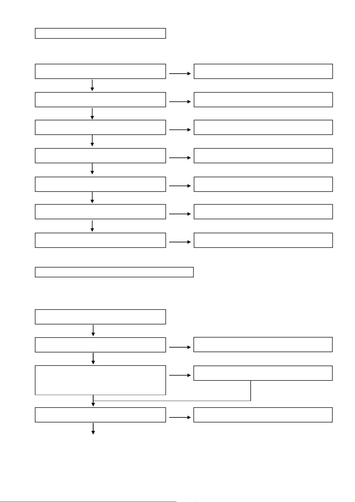
CHAPTER 3. FLOWCHART
[1] Troubleshooting
3 – 1
Page 11
( 1 ) Focus error system check.
Although a CD or DVD is inserted and the cover is closed,
" NO DISC " is displayed.
No Check incoming servo supply ( U5 ).
Yes
2. Is it Open / Close function OK ? No Check Open / Close switch.
Yes
3. Is Sled able to move to inner ? No Check Sled circuit, A5888 ( Pin 23 ).
Yes
4. Is the laser lit ? No Check Laser circuit, CD / DVD Laser circuits.
Yes
5. Does the focus ( lens ) move up and down ? No Check U5 ( Pin 18 ) and U10 ( Pin 13and 14).
Yes
6. Is the turntable rotating ? No Check U5 ( Pin 13 ) and U10 ( Pin 11 and 12 ).
Check Spindle motor.
Yes
7. Is it the CD / DVD Laser driver circuit OK ?
No Check the CD / DVD Laser driver ( Q12, Q13, Q14 &
Q15 ) peripheral circuit and U5 ( Pin 10 and 11).
( 2 ) Both Video and Audio do not operate normally
The RF waveform is normal and the time is
displayed normally, but no sound is produced.
Or the sound has dropouts.
1. Put a disc on DISC compartment.
Yes
2. When playback starts does the disc initialise ? No Repeat steps as Focus errror system check occurred.
Yes
3. Are the RF signal level output from U5 No Is the objective lens of optical pickups clean ?
pin no 168 normal?
( Waveform drawing Figure 1 for CD and
Figure 2 for DVD )
Yes
Yes
4. Replace Servo PWB. No Replace optical pickup mechanism unit.
Yes
1. Does the servo supply is + 3.3 V?
HT-CN9900DVW
3 – 2
Page 12
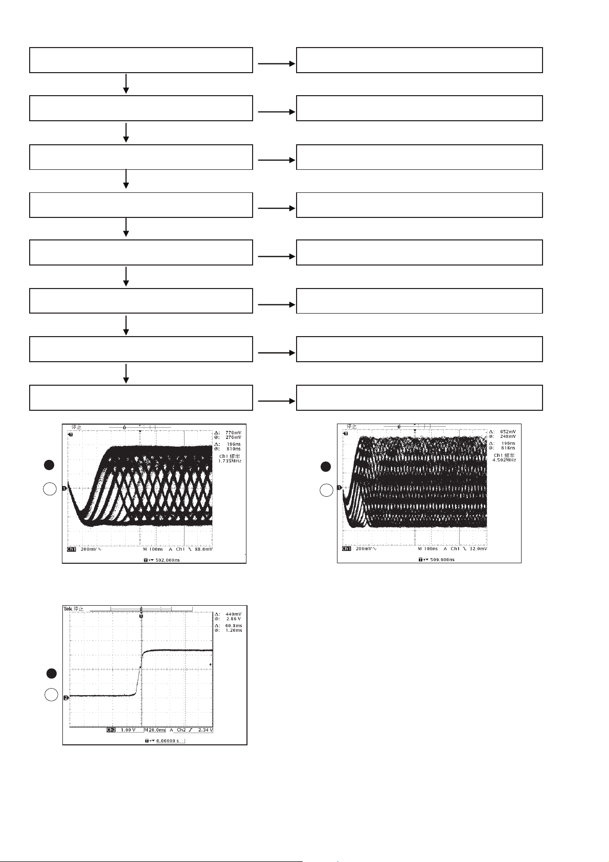
HT-CN9900DVW
5. Does the supply shows as + 3.3 V / + 1.8 V?
No
Check supply ( U1
2
Pin No.2 / U12 Pin No.2 ).
Yes
6. Is Reset function OK? No Check U5 pin no 44.
( Waveform drawing Figure 3 )
Yes
7. Is clock frequency shows 27MHz? No Check clock circuit ( Y2 , C169 , C170 )
Yes
1
8. Is the Flash is normal? No Check U5 pin no
4.
Yes
9. Is the SDRAM is normal? No Check U4 pin no 38.
Yes
10. Is the DSP is normal? No Check U5 Data Bus.
Yes
11. Is the Audio out is normal?
No
Check Audio out circuit ( U5 Pin No.158 and 160 ).
Yes
12. Is the Video out is normal? No
1
1
U5 168
U5 44
RF
Figure 1
1
3
RESET
Check Video out circuit ( U5 Pin no 139 )
1
2
U5 168
RF
Figure 2
Figure 3
3 – 3
Page 13

CHAPTER 4. MAJOR PART DRAWING
Pin
No.
NAME
Alternative
Function
Type Description
Analog Interface ( 66 Pins )
167 RFIP Analog Input AC coupled DVD RF signal input RFIP
168 RFIN OPOUT Analog Input AC coupled DVD RF signal input RFIN
169 RFG OPINP Analog Input Main beam, RF AC input path
170 RFH OPINN Analog Input Main beam, RF AC input path
171 RFA Analog Input RF main beam input A
172 RFB Analog Input RF main beam input B
173 RFC Analog Input RF main beam input C
174 RFD Analog Input RF main beam input D
175 RFE Analog Input RF sub beam input E
176 RFF Analog Input RF sub beam input F
1 AVDD18_2 Analog Power Analog 1.8V power
2 AVDD33_1 Analog Power Analog 3.3V power
3 XTALI Input 27MHz crystal input
4 XTALO Output 27MHz crystal output
5 AGND33 Analog Ground Analog 3.3V Ground
6 V20 Analog Output Reference Voltage 2.0V
7 V14 Analog Output Reference Voltage 1.4V
8 REXT GPO5
Analog Input /
Digital Output
1. Current reference input. It generates reference current for RF
path. Connect an external 15K resistor to this pin and AVSS.
2. GPO5
9 MDI1 Analog Input Laser power monitor input
10 LDO1 Analog Output Laser driver output
11 LDO2 Analog Output Laser driver output
12 AVDD33_2 Analog Power Analog 3.3V power
13 DMO Analog Output Disc motor control output. PWM output
14 FMO Analog Output Feed motor control. PWM output
15 TRAY_OPEN Analog Output Tray PWM output / Tray open output
16 TRAY_CLOSE Analog Output Tray PWM output / Tray close output
17 TRO Analog Output Tracking servo output. PDM output of tracking servo compensator.
18 FOO Analog Output Tracking servo output. PDM output of tracking servo compensator.
19 FG GPIO2 Analog Output
1) Motor Hall sensor input
2) GPIO2
20 USB_DP Analog Inout USB port DPLUS analog pin
21 USB_DM Analog Inout USB port DMINUS analog pin
22 VDD33_USB USB Power USB Power pin 3.3V
23 VSS33_USB USB Ground USB Ground pin 3.3V
24 PAD_VRT Analog Inout USB generating reference current
25 VDD18_USB USB Power USB Power pin 1.8V
112 AGND33_VPLL Analog Ground Analog 3.3V Ground
113 EXT_RES Analog Input External Resistor for HDMi ™ TX
[1] Function Table Of IC
U5 VHIMT1389GF-1Q : High Definition DVD Player SOC with HDMi (1/9)
HT-CN9900DVW
4 – 1
Page 14

HT-CN9900DVW
U5 VHIMT1389GF-1Q : High Definition DVD Player SOC with HDMi (2/9)
Pin
No.
114 AVDD33_VPLL Analog Power 3.3V VDD for HDMi ™ TX
115 AGND33_TX Analog Ground Analog 3.3V Ground
116 AGND18_TX2 Analog Ground Analog 1.8V Ground
117 TXCN Analog Output Negative TX CLK
118 TXCP Analog Output Positive TX CLK
119 AVDD18_TX1 Analog Power 1.8V VDD for HDMi ™ TX
120 TX0N Analog Output Negative TX CH0
121 TX0P Analog Output Positive TX CH0
122 AGND18_TX1 Analog Power 1.8V GND for HDMi ™ TX
123 TX1N Analog Output Negative TX CH1
124 TX1P Analog Output Positive TX CH1
125 AGND18_TX0 Analog Power 1.8V VDD for HDMi ™ TX
126 TX2N Analog Output Negative TX CH1
127 TX2P Analog Output Positive TX CH2
128 AGND18_TXD Analog Ground Analog 1.8V Ground
134 DACVDDC Power 3.3V Power pin for video DAC circuitry
135 VREF GPIO14
136 FS Analog Full scale adjustment (suggest to use 560 ohm)
137 DACVSSC Analog Ground Analog 3.3V Ground
138 CVBS Analog Analog CVBS or C
139 DACVDDB Power 3.3V Power pin for video DAC circuitry
140 AGNDC Analog Ground Analog 3.3V Ground
141 DACVDDA Power 3.3V Power pin for video DAC circuitry
142 Y / G Analog Green, Y, SY or CVBS
143 AGNDB Analog Ground Analog 3.3V Ground
144 B / CB / PB Analog Blue, CB / PB or SC
145 R / CR / PR Analog Red, CR / PR, CVBS or SY
146 AADVSS Analog Ground Analog 3.3V Ground
147 AKIN2 GPIO19 Analog
148 ADVCM GPIO20 Analog
149 AKIN1 GPIO21 Analog
150 AADVDD Power 3.3V Power pin for 2ch audio ADC circuitry
151 APLLVDD3 Power 3.3V Power pin for audio clock circuitry
152 APLLCAP Analog InOut APLL external capacitance connection
NAME
Alternative
Function
Type Description
Analog /
Digital Output
1.Bandgap reference voltage
2.GPO14
1. Audio ADC input 2
2. MCDATA
3. Audio Mute
4. HSYN / VSYN output
5. SPDIF output 2
6. GPIO
1.Hotplug
2.GPIO
1.Audio ADC input 1
2.Audio Mute
3.HSYN / VSYN output
4.GPIO
4 – 2
Page 15
U5 VHIMT1389GF-1Q : High Definition DVD Player SOC with HDMi (3/9)
HT-CN9900DVW
Pin
No.
153 APLLVSS Analog Ground Analog 3.3V Ground
154 ADACVSS2 Analog Ground Analog 3.3V Ground
155 ADACVSS1 Analog Ground Analog 3.3V Ground
156 ARF / LFE GPIO Analog Output
157 ARS GPIO Analog Output
158 AR GPIO Analog Output
159 AVCM Analog Audio DAC reference voltage
160 AL GPIO Analog Output
161 ALS GPIO Analog Output
162 ALF / CENTER GPIO Analog Output
163 ADACVDD1 Analog Power 3.3V Power pin for audio DAC circuitry
164 ADACVDD2 Analog Power 3.3V Power pin for audio DAC circuitry
165 AVDD18_1 Analog Power Analog 1.8V power
167 AGND18 Analog Ground Analog 1.8V Ground
79,
109
38,57,
67,92,
101
98 DVSS18 Ground 1.8V ground pin for internal digital circuitry
96 DVSS33 Ground 3.3V ground pin for internal digital circuitry
NAME
DVDD18 Power 1.8V power pin for internal digital circuitry
DVDD33 Power 3.3V power pin for internal digital circuitry
Alternative
Function
Type Description
1.Audio DAC sub-woofer channel output
2.While internal audio DAC not used
a.ACLK
b.HSYN / VSYN output
c.GPIO
1.Audio DAC right surround channel output
2.While internal audio DAC not used
a.ABCK
b.HSYN / VSYN output
c.GPIO
1.Audio DAC right channel output
2.While internal audio DAC not used
a.SDATA2
b.RXD2
c.GPIO
1.Audio DAC left channel output
2.While internal audio DAC not used
a.SDATA1
b.TXD2
c.GPIO
1.Audio DAC left surround channel output
2.While internal audio DAC not used
a.ALRCK
b.GPIO
1.Audio DAC center channel output
2.While internal audio DAC not used
a.ASDATA0
b.Audio Mute
c.GPIO
General Power (7)
General Ground (2)
Micro Controller, Flash Interface and GPIO (11)
4 – 3
Page 16

HT-CN9900DVW
U5 VHIMT1389GF-1Q : High Definition DVD Player SOC with HDMi (4/9)
Pin
No.
46 GPIO3 INT#
47 GPIO4
43 GPIO6
35 SF_CS_
36 SF_DO
37 SF_DI
39 SF_CK
40 UP1_6 SCL
41 UP1_7 SDA
44 PRST#
45 IR GPI
68 RD0
69 RD1
70 RD2
71 RD3
72 RD4
73 RD5
74 RD6
75 RD7
NAME
Alternative
Function
Type Description
InOut
8mA, SR
SMT
InOut
4mA, PD
InOut
4mA, PD
InOut
8mA, SR
PU, SMT
InOut
8mA, SR
PD, SMT
InOut
8mA, SR
PU, SMT
InOut
8mA, SR
PD, SMT
InOut
4mA, SR
PU, SMT
InOut
4mA, SR
PU, SMT
Input
4mA, SR
PU, SMT
Input
4mA, SR
SMT
Dram Interface (37) (Sorted by position)
InOut
2mA
InOut
2mA
InOut
2mA
InOut
2mA
InOut
2mA
InOut
2mA
InOut
2mA
InOut
2mA
1.General purpose IO 3
2.Microcontroller port 3-1
3.Microcontroller external interrupt 1
1.General purpose IO 4
2.SD_CLK set B
3.Microcontroller port 3-4 (Internal Pull-up)
1.General purpose IO 6
2.Microcontroller port 3-5 (Internal Pull-up)
1.Serial Flash Chip Select
2.Trap value in power-on reset:
1: Serial Flash ATMEL mode
0: Serial ST / SST mode
Serial Flash Dout
1.Serial Flash Din
2.Trap value in power-on reset:
1: Manufactory Test Mode
0: Normal Operation
Serial Flash Clock
1.Microcontroller port 1-6
2.1²C clock pin
3.Trap value in power-on reset:
1: Manufactory test mode
0: Normal operation
1.Microcontroller port 1-7
2.1²C data pin
3.Trap value in power-on reset:
1: Manufactory test mode
0: Normal operation
Power on reset input, active low
1.IR control signal input
2.GPI
DRAM data 0
DRAM data 1
DRAM data 2
DRAM data 3
DRAM data 4
DRAM data 5
DRAM data 6
DRAM data 7
4 – 4
Page 17

U5 VHIMT1389GF-1Q : High Definition DVD Player SOC with HDMi (5/9)
HT-CN9900DVW
Pin
.
No
76 DQM0
77 RD15
78 RD14
80 RD13
81 RD12
82 RD11
83 RD10
84 RD9
85 RD8
86 DQM1
87 RCLK
88 RA11
89 RA9
90 RA8
91 RD7
93 RA6
94 RA5
95 RA4
97 RWE#
99 CAS#
100 RAS#
102 BA0
103 BA1
104 RA10
105 RA0
106 RA1
107
108 RA3
NAME
RA2
Alternative
Function
Type Description
InOut
2mA, PD
InOut
2mA
InOut
2mA
InOut
2mA
InOut
2mA
InOut
2mA
InOut
2mA
InOut
2mA
InOut
2mA
InOut
2mA, PD
InOut
2mA, PD
InOut
2mA, PD
InOut
2mA, PD
InOut
2mA, PD
InOut
2mA, PD
InOut
2mA, PD
InOut
2mA, PD
InOut
2mA, PD
Output
2mA, PD
Output
2mA, PD
Output
2mA, PD
InOut
2mA, PD
InOut
2mA, PD
InOut
2mA, PD
InOut
2mA, PD
InOut
2mA, PD
InOut
2mA, PD
InOut
2mA, PD
Data mask 0
DRAM data 15
DRAM data 14
DRAM data 13
DRAM data 12
DRAM data 11
DRAM data 10
DRAM data 9
DRAM data 8
Data mask 1
DRAM clock
DRAM address bit 11
DRAM address 9
DRAM address 8
DRAM address 7
DRAM address 6
DRAM address 5
DRAM address 4
DRAM Write enable, active low
DRAM column address strobe, active low
DRAM row address strobe, active low
DRAM bank address 0
DRAM bank address 1
DRAM address 10
DRAM address 0
DRAM address 1
DRAM address 2
DRAM address 3
4 – 5
Page 18

HT-CN9900DVW
U5 VHIMT1389GF-1Q : High Definition DVD Player SOC with HDMi (6/9)
Pin
No.
66 GPIO7 CKE
65 GPIO8
64 GPIO9
111 GPIO10
42 GPIO11
38 SPDIF GPIO12
63 GPIO13
26 YCLK
27 DV_Y0
28 DV_Y1
29 DV_Y2
30 DV_Y3
31 DV_Y4
32 DV_Y5
NAME
Alternative
Function
Type Description
1. GPIO7
2. DRAM Clock Enable
I nO ut
4mA, PD
GPIO (29)
I nO ut
4mA, PD
I nO ut
4mA, PD
I nO ut
4mA, PD
InOut
4mA
I nO ut
2mA, PD
I nO ut
4mA, PD
I nO ut
2mA, PD
I nO ut
2mA, PD
I nO ut
2mA, PD
I nO ut
2mA, PD
I nO ut
2mA, PD
I nO ut
2mA, PD
I nO ut
2mA, PD
3. MS_CLK set A
4. SD_CLK set A
5. HSYN / VSYN input
6. Microcontroller port 1~4 (Internal Pull-Up)
1. GPIO8
2. MS_BS set A
3. SD_CMD set A
4. ASDATA2
5. ACLK
6. Audio Mute
7. HSYN / VSYN input
8. Microcontroller port 1~5 (Internal Pull-Up)
1. GPIO9
2. MS_D0 set A
3. SD_D0 set A
4. ASDATA2
5. ABCK
6. RXD1
1. GPIO10
2. ASDATA0
3. ALRCK
4. HSYN / VSYN output
5. TXD1
1. GPIO11
2. SD_CMD set B
3. MS_BS set B
4. Audio Mute
5. HSYN / VSYN output
6. Microcontroller port 3-0 (Internal Pull-Up)
1. SPDIF output
2. GPIO12
1. GPIO13
2. SD_D0 set B
3. ALRCK
4. Audio Mute
GPIO
GPIO
GPIO
GPIO
GPIO
GPIO
GPIO
4 – 6
Page 19

U5 VHIMT1389GF-1Q : High Definition DVD Player SOC with HDMi (7/9)
HT-CN9900DVW
Pin
No.
33 DV_Y6
34 DV_Y7
48 DV_C0
49 DV_C1
50 DV_C2
51 DV_C3
52 DV_C4
53 DV_C5
54 DV_C6
55 DV_C7
56 SD_MS_CLK
58 SD_MS_CMD
59 SD_MS_D0
60 SD_MS_D1
61 SD_MS_D2
62 SD_MS_D3
NAME
Alternative
Function
Type Description
I nO ut
2mA, PD
I nO ut
2mA, PD
I nO ut
4mA, PD
I nO ut
4mA, PD
I nO ut
4mA, PD
I nO ut
4mA, PD
I nO ut
4mA, PD
I nO ut
4mA, PD
I nO ut
2mA, PD
I nO ut
2mA, PD
I nO ut
2mA, PD
I nO ut
2mA, PD
I nO ut
2mA, PD
I nO ut
2mA, PD
I nO ut
2mA, PD
I nO ut
2mA, PD
GPIO
GPIO
GPIO
GPIO
GPIO
GPIO
1) GPIO
2) SD_D2
1) GPIO
2) SD_D3
GPIO
GPIO
1) GPIO
2) SD_CLK
3) MS_CLK
1) GPIO
2) SD_CMD
3) MS_BS
1) GPIO
2) SD_D0
3) MS_D0
1) GPIO
2) SD_D1
3) MS_D1
1) GPIO
2) SD_D2
3) MS_D2
1) GPIO
2) SD_D3
3) MS_D3
Notes:
1. The Main column is the main function, Alt. means alternative function.
2. The multi-function GPIO pins are set to green characters.
4 – 7
Page 20

HT-CN9900DVW
U5 VHIMT1389GF-1Q : High Definition DVD Player SOC with HDMi (8/9)
HDMI 1.2 Tx
HDMI Tx
DVD
PUH
Module
Motor
Drive
FLASH
ROM
DRAM
RF Amplifier
Servo IO
Spindle
Control
Memory
Controller
Debug
Port
Servo
Processor
Audio
DSP
System
Parser
CPPM/CPRM
DRM
108MHz
TV Encoder
Video
Processor
Video Decoder
Audio
Ouptut
Video DAC
interlacer
MPEG-1/2
JPEG
Audio DAC
De-
PCM
CVBS, Y/C
Component
Video
Digital Video
External
Audio DAC
GPIO
IR/VFD
System
CPU
32-bit
RISC
USB2.0
MS/SD/MMC
Controller
Figure 4-1 BLOCK DIAGRAM OF IC
SPDIF
USB
device
MS/SD/MMC
Card
4 – 8
Page 21

U5 VHIMT1389GF-1Q : High Definition DVD Player SOC with HDMi (9/9)
Figure 4-2 BLOCK DIAGRAM OF IC
RFF
RFE
RFD
RFC
RFB
RFA
RFH / OPINN
RFG / OPINP
RFIN / OPOUT
RFIP
AGND1
8
AVDD18_1
ADACVDD2
ADACVDD1
CENTER / GPIO
ALS / GPIO
AL / GPIO
AVCM
AR / GPIO0
ARS
/ GPIO
LFE / GPIO
ADACVSS1
ADACVSS2
APLLVSS
APLLCAP
APLLVDD
AADVDD
AKIN1 / GPIO21
ADVCM / GPIO20
AKIN2 / GPIO19
AADVSS
R
B
AGNDC
G
DACVDDA
AGNDC
DACVDDB
CVBS
DACV
SSC
FS
VREF / GPIO14
DACVDDC
NC
176
175
174
17
3
172
171
170
169
168
167
166
165
164
163
162
161
160
159
158
157
156
155
154
15
3
152
151
150
149
148147
146
145
144
143
142
141
140
139
138137
136
1
3
5
134
1
33
AVDD18_2 1 132NC
AVDD33_1 2 131NC
XTALI 3 130NC
XTALO 4 129 NC
AGND33 5 128 AGND18_TXD
V20 6 127 TX2P
V14 7 126 TX2N
REXT / GPO5 8 125 AVDD18_TX0
MDI1 9 124 TX1P
LDO1 10 123 TX1N
LDO2 11 122 AGND18_TX1
AVDD33_2 12 121 TX0P
DMO
13 120 TX0N
FMO 14 119 AVDD18_TX1
TRAY_OPEN 15 118 TXCP
TRAY_CLOSE16 117 TXCN
TRO 17 116 AGND18_TX2
FOO 18 115 AGND33_TX
FG / GPIO2 19 114 AVDD33_VPLL
USB_DP 20 113 EXT_RES
USB_DM 21 112 AGND33_VPLL
VDD
33_USB22 111 GPIO10 / HPLG
VSS33_U
SB23 110 SPDIF / GPIO12
PAD_VRT 24 109 DVDD18
VDD18_USB25 108 RA3
YCLK 26 107 RA2
DV_Y0 27 106 RA1
DV_Y1 28 105 RA0
DV_Y2 29 104 RA10
DV_Y330 103 BA1
DV_Y4 31 102 BA0
DV_Y5 32 101 DVDD33
DV_Y6 33 100 RAS_
DV_Y7 34 99 CAS_
SF_CS_ 35 98 GND18
SF_DO 36 97 RWE_
SF_DI 37 96 GND33
DVDD33 38 95 RA4
SF_CK 3
9 94 RA5
UP1_6 / SCL 40 93 RA6
UP1_7 / SDA 41 92 DVDD33
GPIO11 42 91 RA7
GPIO6 43 90 RA8
PRS
T_ 44 89RA9
45
4647484950515253
545556
57
58
59
606162
63
64
65
666768
697071
72
73
74
75
76
77
78
79
80
81
82
83
8485
86
8788
IR
GPIO3
/ INT
GPIO4
DV_C0
DV_C1
DV_C2
DV_C
3
DV_C4
DV_C5
DV_C6
DV_C7
S
D_M
S_CLK
DVDD
33
SD_M
S
_CMD
SD_M
S_DO
SD_MS_D1
SD_M
S
_D2
SD_MS_D3
GPIO13
GPIO9
GPIO8
GPIO7 / CKE_
DVDD
33
RD0
RD1
RD2
RD3
RD4
RD5
RD6
RD7
DQM0
RD15
RD14
DVDD18
RD1
3
RD12
RD11
RD10
RD9
RD8
DQM1
RCLK
RA1
1
MT1389M
HT-CN9900DVW
4 – 9
Page 22

HT-CN9900DVW
VFD701 VVKHLD1321W-1
GRID ASSIGNMENT
OUTER DIMENSIONS
PATTERN AREA
131
[2] VFD Display
4 – 10
Page 23

CHAPTER 5. CIRCUIT DESCRIPTION
U5
U5
U5
U5
13
14
U5
U5
U5
U5
U2
U5
U2
Figure 1
Figure 2
Figure 3 Figure 4
Figure 5 Figure 6
R OUT
L OUT
TRO
FMO
FOO
MD11
Pin 15
LD01
LD02
DMO
1
2
17
18
3
4
9
15
5
6
10
11
7
8
24
9
23
10
168
11
RF
168
U5
12
44
U5
13
RF
RESET
Figure 7 Figure 8
[1] Waveform Of Servo Circuit
HT-CN9900DVW
5 – 1
Page 24

HT-CN9900DVW
14
CVBS OUT
138
U5
Figure 9
5 – 2
Page 25

[2] Voltage
1 0.000 9 0.026
2 0.023 10 0.021
3 0.000 11 2.429
4 1.873 12 0.000
5 0.045 13 0.000
6 0.000 14 0.203
7 0.000 15 0.766
8 0.000 16 6.080
1 1.245 45 5.120 89 0.006 133 0.001
2 3.306 46 2.623 90 0.005 134 3.306
3 0.773 47 2.739 91 0.005 135 3.305
4 0.473 48 3.292 92 3.303 136 0.741
5 0.000 49 3.292 93 0.059 137 0.000
6 1.976 50 3.292 94 0.055 138 0.000
7 1.397 51 1.777 95 0.059 139 3.286
8 1.245 52 0.002 96 0.005 140 3.306
9 0.000 53 0.005 97 3.300 141 0.000
10 3.254 54 0.013 98 0.003 142 0.000
11 3.254 55 0.005 99 3.299 143 0.000
12 3.291 56 0.013 100 3.297 144 0.000
13 1.391 57 3.303 101 3.303 145 0.001
14 1.391 58 0.005 102 0.052 146 2.290
15 0.000 59 1.759 103 0.003 147 2.209
16 0.000 60 0.005 104 0.005 148 0.001
17 1.393 61 0.004 105 0.028 149 1.658
18 1.396 62 0.004 106 0.030 150 1.629
19 0.000 63 0.003 107 0.059 151 3.306
20 0.010 64 0.019 108 1.293 152 3.305
21 0.012 65 3.287 109 1.313 153 0.001
22 3.304 66 2.588 110 0.002 154 0.001
23 0.000 67 3.303 111 0.003 155 0.001
24 0.000 68 0.004 112 0.002 156 1.635
25 1.338 69 0.003 113 3.299 157 1.644
26 0.014 70 0.003 114 3.303 158 0.002
27 2.654 71 0.004 115 0.000 159 1.510
28 3.304 72 0.003 116 0.000 160 0.002
29 0.026 73 0.003 117 0.001 161 1.651
30 0.018 74 0.004 118 0.001 162 0.001
31 0.019 75 0.005 119 1.342 163 3.301
32 0.005 76 3.301 120 0.826 164 3.301
33 3.324 77 0.005 121 0.791 165 1.240
34 3.324 78 0.005 122 0.000 166 0.000
35 3.295 79 1.313 123 0.839 167 0.000
36 0.005 80 0.006 124 1.342 168 0.000
37 0.005 81 0.006 125 1.318 169 1.577
38 3.304 82 0.006 126 0.432 170 1.576
39 0.016 83 0.006 127 0.731 171 0.462
40 0.005 84 0.006 128 0.000 172 0.462
41 0.005 85 0.006 129 0.000 173 0.453
42 3.305 86 2.937 130 0.013 174 0.456
43 3.304 87 1.505 131 0.016 175 0.042
44 3.282 88 0.016 132 0.002 176 0.041
PINNOVOLTAGE
(V)
PINNOVOLTAGE
(V)
U2
U5
PINNOVOLTAGE
(V)
PINNOVOLTAGE
(V)
PINNOVOLTAGE
(V)
PINNOVOLTAGE
(V)
HT-CN9900DVW
5 – 3
Page 26

HT-CN9900DVW
PINNOVOLTAGE
1 3.304 15 3.302 29 1.115 43 3.299
2 0.002 16 3.300 30 1.113 44 0.524
3 3.304 17 3.301 31 1.088 45 0.522
4 0.002 18 3.298 32 0.043 46 0.001
5 0.002 19 0.000 33 0.008 47 0.544
6 0.000 20 0.001 34 0.009 48 0.559
7 0.002 21 0.001 35 0.010 49 3.299
8 0.002 22 0.004 36 0.023 50 0.622
9 3.304 23 0.001 37 3.296 51 0.618
10 0.002 24 0.001 38 1.507 52 0.001
11 0.002 25 0.001 39 2.725 53 0.588
12 0.000 26 0.001 40 0.036 54 0.001
13 0.002 27 3.394 41 0.001
14 3.304 28 0.000 42 0.001
(V)
PINNOVOLTAGE
(V)
U4
PIN
NO
VOLTAGE
(V)
PINNOVOLTAGE
(V)
U10
PINNOVOLTAGE
(V)
1 1.394 1 0.000 13 0.000 25 3.301
2 5.000 2 0.000 14 0.000 26 3.307
3 1.414 3 0.000 15 36.770 27 3.307
4 1.392 4 36.770 16 0.000 28 3.310
5 1.425 5 0.000 17 0.000 29 0.012
6 0.001 6 0.000 18 0.005 30 0.009
7 0.108 7 36.770 19 0.000 31 0.001
8 0.000 8 0.003 20 0.013 32 0.001
9 5.230 9 0.003 21 4.890 33 24.980
10 0.000 10 0.000 22 4.890 34 24.980
11 0.000 11 0.000 23 3.313 35 36.770
12 1.579 12 36.770 24 0.000 36 36.770
13 1.579
14 1.475
15 1.475
16 1.475
17 1.475 1 0.000 13 0.000 25 3.301
18 1.463 2 0.000 14 0.000 26 3.307
19 1.463 3 0.000 15 36.770 27 3.307
20 5.230 4 36.770 16 0.000 28 3.310
21 1.915 5 0.000 17 0.000 29 0.012
22 5.230 6 0.000 18 0.005 30 0.009
23 0.000 7 36.770 19 0.000 31 0.001
24 0.000 8 0.003 20 0.013 32 0.001
25 0.347 9 0.003 21 4.890 33 24.980
26 5.200 10 0.000 22 4.890 34 24.980
27 5.210 11 0.000 23 3.313 35 36.770
28 0.142 12 36.770 24 0.000 36 36.770
29 0.002
30 0.002
U9
PINNOVOLTAGE
(V)
1 3.290 3 3.302 3 5.230
2 3.321 4 0.000
3 0.004 5 0.002
4 0.000 6 0.001
PIN
VOLTAGE
NO
PINNOVOLTAGE
PINNOVOLTAGE
1 3.295 1 0.000
2 0.002 2 3.306
7 3.302
8 3.306 1 0.000
(V)
(V)
U14 U12
(V)
U6
PINNOVOLTAGE
(V)
U7
PINNOVOLTAGE
(V)
PINNOVOLTAGE
(V)
U13
PINNOVOLTAGE
(V)
2 1.342
3 4.490
PINNOVOLTAGE
(V)
PINNOVOLTAGE
(V)
5 – 4
Page 27

HT-CN9900DVW
1 0.000 13 0.000 25 3.301 1
11.520
2 0.000 14 0.000 26 3.307 2
11.490
3 0.000 15 36.770 27 3.307 3
12.030
4 36.770 16 0.000 28 3.310 4
0.000
5 0.000 17 0.000 29 0.012 5
12.030
6 0.000 18 0.005 30 0.009 6
11.480
7 36.770 19 0.000 31 0.001 7
11.540
8 0.003 20 0.013 32 0.001 8
12.050
9 0.003 21 4.890 33 24.980
10 0.000 22 4.890 34 24.980
11 0.000 23 3.313 35 36.770
12 36.770 24 0.000 36 36.770
1 0.000 17 0.000 33 0.000 49 0.010
2 0.000 18 0.000 34 0.000 50 0.000
3 3.300 19 3.298 35 3.303 51 0.000
4 0.000 20 3.298 36 0.000 52 3.302
5 0.000 21 0.854 37 0.007 53 0.000
6 0.002 22 0.860 38 0.001 54 0.000
7 0.002 23 0.000 39 0.001 55 3.302
8 0.002 24 0.004 40 0.001 56 0.000
9 1.234 25 3.295 41 0.014 57 0.000
10 1.650 26 1.648 42 0.009 58 3.303
11 1.644 27 0.000 43 0.012 59 0.000
12 3.300 28 3.300 44 3.303 60 0.000
13 0.000 29 0.000 45 0.000 61 0.000
14 0.000 30 0.000 46 0.000 62 0.000
15 3.297 31 0.000 47 0.002 63 0.000
16 0.000 32 0.000 48 0.002 64 3.298
1
2.484
14
-27.290
27
-29.140
40
0.000
2
0.000
15
0.024
28
-24.740
41
0.000
3
0.000
16
-27.310
29
-27.140
42
0.000
4
0.000
17
-27.300
30
-20.050
43
0.000
5
0.000
18
1.525
31
-27.160
44
2.936
6
0.000
19
-27.28
32
-26.810
45
3.240
7
0.000
20
-30.030
33
-20.050
46
0.000
8
5.060
21
5.070
34
-27.140
47
3.389
9
-27.450
22
-29.350
35
-24.820
48
3.389
10
-27.450
23
-27.330
36
-29.530
49
1.210
11
-27.320
24
-29.700
37
-22.430
50
5.060
12
-27.320
25
-17.820
38
-17.310
51
5.060
13
-27.320
26
-22.560
39
5.070
52
1.322
1
3.270
2
0.000
3
5.050
U11
PINNOVOLTAGE
(V)
PINNOVOLTAGE
(V)
PINNOVOLTAGE
(V)
VOLTAGE
(V)
U701
PINNOVOLTAGE
(V)
VOLTAGE
(V)
U8
U501
PINNOVOLTAGE
(V)
PIN
NO
PINNOVOLTAGE
(V)
PINNOVOLTAGE
(V)
VOLTAGE
(V)
PIN
NO
PIN
NO
U702
VOLTAGE
(V)
VOLTAGE
(V)
PIN
NO
VOLTAGE
(V)
PIN
NO
PIN
NO
5 – 5
Page 28

HT-CN9900DVW
1
0.400m
11
0.300m
1
0.100m
B
2.429
2
0.300m
12
1.636
2
3.300
C
5.220
3
0.600m
13
3.286
3
5.210
E
1.737
4
0.200m
14
0.400m
5
3.066
15
1.638
6
0.600m
16
1.638
7
1.643
17
1.628
8
0.200m
18
1.637
B
0.685
G
0.029
9
1.630
19
1.633
C
0.030
D
0.000
10
1.632
20
0.000
E
0.000
S
0.000
G
2.160
B
0.014
G
5.080
B
3.289
D
5.140
C
5.100
D
0.000
C
3.290
S
3.387
E
0.000
S
0.000
E
3.303
B
0.645
B
0.030
B
3.288
B
0.648
C
20.700m
C
5.100
C
3.291
C
0.026
E
0.000
E
0.000
E
3.301
E
0.000
B
3.304
B
3.304
B
3.982
B
26.10m
C
262.50m
C
64.0m
C
5.110
C
3.298
E
3.306
E
3.306
E
3.282
E
0.000
B
5.200
G
0.001
B
0.570
C
5.040
D
2.731
C
0.026
E
0.531
S
0.525
E
0.000
Q18
PINNOVOLTAGE
(V)
Q19
PINNOVOLTAGE
(V)
Q14
PINNOVOLTAGE
(V)
Q20
PINNOVOLTAGE
(V)
Q21
PINNOVOLTAGE
(V)
PINNOVOLTAGE
(V)
PINNOVOLTAGE
(V)
Q17
PINNOVOLTAGE
(V)
Q16
Q3
PINNOVOLTAGE
(V)
Q12
PINNOVOLTAGE
(V)
Q13
PINNOVOLTAGE
(V)
Q7
PINNOVOLTAGE
(V)
Q9
PINNOVOLTAGE
(V)
IC2
PINNOVOLTAGE
(V)
PINNOVOLTAGE
(V)
PINNOVOLTAGE
(V)
IC1
PINNOVOLTAGE
(V)
PIN
NO
Q4
PINNOVOLTAGE
(V)
Q10
Q11
PINNOVOLTAGE
(V)
Q15
VOLTAGE
(V)
PINNOVOLTAGE
(V)
Q1
Q2
5 – 6
Page 29

-MEMO-
HT-CN9900DVW
5 – 7
Page 30

HT-CN9900DVW
CHAPTER 6. DIAGRAM
[1] Block Diagram
Fan
FR SPK
FM ANT
AMP
Pack
Tuner
FLASH
EN25B160
AT25FS160/
FL SPK
AMP
STA51 0
CEN SPK
P
AMP AMP
SR SPK
STA510
+30V
+3.3V
+1.2V
SL SPK
PCM
AMP
1117Y33L
1117H12E
SUB SPK
AMP
STA510
SMPS
+5.0V
IIS and DATA
OUTPUT
DATA
SW
VIDEO
HDMI
AUDIO
DATA
DATA
AUDIO
DATA
2
MIC
1
MIC
DOOR
PICK UP
HEADER
DATA
DISC
MOTOR
UX
IN
LR
A
IN
AUX
BM
WM8782
CD4052
MOTOR
MOTOR
AN5888
Motor drive
SDRAM
EM638165
Figure 6-1: BLOCK DIAGRAM
6 – 1
Page 31

HT-CN9900DVW
•Resistor:
To differentiate the units of resistors, such symbol as
K and M are used: the symbol K means 1000 ohm
and the symbol M means 1000 kohm and the
resistor without any symbol is ohm-type resistor.
Besides, the one with “Fusible” is a fuse type
• Capacitor:
To indicate the unit of capacitor, a symbol P is used:
this symbol P means pico-farad and the unit of the
capacitor without such a symbol is microfarad. As to
electrolytic capacitor, the expression “capacitance/
withstand voltage” is used.
(CH), (TH), (RH), (UJ): Temperature compensation
(ML): Mylar type
(P.P.): Polypropylene type
• Schematic diagram and Wiring Side of P.W.Board
for this model are subject to change for
improvement without prior notice.
• The indicated voltage in each section is the one
measured by Digital Multimeter between such a
section and the chassis with no signal given.
• Parts marked with “ ” are important for
maintaining the safety of the set. Be sure to replace
these parts with specified ones for maintaining the
safety and performance of the set.
PWB Switch Location
!
REF. NO DESCRIPTION POSITION
SW701 POWER ON/STAND-BY ON—OFF
SW702 STOP
SW703
SW704
ON—OFF
PLAY / PAUSE ON—OFF
OPEN / CLOSE
ON—OFF
TOP VIEW FRONT VIEW
KTC3875GR
KN3904S
KN3906S
SMPS8550S
SMPS8050S
PST8229U
2SK3018 (MOSFET)
BAV99
304VT
DA1010
TOP VIEW
TOP VIEW
TOP VIEW
EXA704WJ
EXA001
B
(2)
G
(2)
E
(1)
S
(1)
C
(3)
D
(3)
TOP
VIEW
TOP
VIEW
KTC4375Y
A2012
B
(1)
E
(3)
C
(2)
TOP
VIEW
1117Y33L
1117H12E
GND
Vin
Vout
TOP
VIEW
TOP
VIEW
GNDOUT
VDD NC
14
23
A
C
(1)
(2)
(3)
BAT54C
ANODE (1)
ANODE (2)
(3) CATHODE
A
C
CHAPTER 7. CIRCUIT SCHEMATICS AND PARTS LAYOUT
[1] Notes On Schematic Diagram
[2] Types Of Transistor And LED
7 – 1
Page 32

HT-CN9900DVW
FAULT
CON2
3P53254
FAULT
/FAULT
[3] Schematic Diagram
MAIN/AMP PWB-A1
A
MAIN SECTION
FAULT
B
CON2
3P53254
C
TO
MECHA ASS’Y
D
E
/FAULT
F
G
HDMI
OUT
FAULT
FROM
CD PICK-UP
UNIT
FROM
USB PWB-A4
Bi401
USB SIGNAL
AUDIO SIGNAL
VIDEO SIGNAL
H
1
2 3 456
TO
SMPS PWB-B
FROM
MIC PWB-A3
Bi501
FROM
LOADER
FROM
DISPLAY PWB-A2
7
8 9 10 11 12
CD SIGNAL
Figure 7-1: MAIN/AMP (MAIN SECTION) SCHEMATIC DIAGRAM
7 – 2
Page 33

MAIN/AMP PWB-A1
FAULT
HT-CN9900DVW
A
AMPLIFIER SECTION
B
C
D
TO
HOME THEATER
SPEAKER SYSTEM
E
F
FAULT
G
FROM
SMPS PWB-B
AUDIO SIGNAL
H
1
2 3 456
Figure 7-2: MAIN/AMP (AMP SECTION) SCHEMATIC DIAGRAM
7
8 9 10 11 12
7 – 3
Page 34

HT-CN9900DVW
B544AWPZ
C402
39P
C403
39P
0.047u
A
B
C
TO
SMPS PWB-B
DISPLAY PWB-A2
MIC PWB-A3
TO
MAIN/AMP PWB-A1
MIC IN 1MIC IN 2
0.047u
D
AUDIO SIGNAL
USB PWB-A4
E
FROM
USB EXTERNAL
F
DEVICE ONLY
USB SIGNAL
G
39P
C402
B544AWPZ
39P
C403
TO
MAIN/AMP PWB-A1
CON6
TO
H
1
2 3 456
MAIN/AMP PWB-A1
7
8 9 10 11 12
Figure 7-3: DISPLAY, MIC & USB SCHEMATIC DIAGRAM
7 – 4
Page 35

[4] Charts Of Connecting Wires
HT-CN9900DVW
SUBWOOFER
A
FM ANTENNA
VIDEO OUT
AUX IN
SURROUND
L-Ch
R-Ch
CENTER
L-Ch
FRONT
R-Ch
MIC 2 MIC 1
US B IN
HDMI IN
SW SL SR CEN FL FR
RCA3
1234
B
TU301
HA1
CON1
241
HDMI
RCA2
Bi2
RD
1234
BK
BK
BK
SP1
PK
GY
WH
BK
1234
GY
MIC502
Bi501
1234
BKWHGY
MIC501
PK
MIC PWB-A3
241
241
Bi1
1
2
RDBKBKBKBKBKBK
FROM
SMPS PWB-B
CON4
6543
89
7
BK
CNS4
RDWHBLWHBL
CN6
FROM
CD/DVD PICK-UP
UNIT
54321
6
543216
CON5 CON6
4321
4321
CNS5
WH
RDBLBK
BL
FROM
CD/DVD LOADER
CON7
5
5
BK
CNS401
BKPKWH
4321
4321
YL
4321765
4321765
CNS702
RDBKBKBKBKBKBK
CON2
MAiN / AMP PWB-A1
YLBKRD
SHIELD WIRE
C
FFC1
TO
D
MECHANISM
BK
TO
CHASSIS
(GND)
LUG402
LUG401
JK401
BI401
BKPKWH
GY
43215
YL
USB PWB-A4
COLOR TABLE
RD
BK
WH
RED
BLACK
WHITE
GY GRAY
BL BLUE
FAN
SHIELD WIRE
E
BR BROWN
PK PINK
YL YELLOW
F
DISPLAY PWB-A2
G
H
1
VOL701
CNS2
BK
BK
Bi1
BK
RD
BK
BK
BK
RD
BK
BK
BK
BK
BK
BK
BK
RD
BKBKBKBKBK
BK
1
LUG701
VFD701
3
1
BKBKBK
RD
RD
4321765
4321
Bi701
Bi702
1
FROM
MAiN / AMP PWB-A1
23456
CNS701
1
2
3
4
CNS1
1
2
3
4
8
567
1234
1
2
CN4
3
4
1
CN5CN6
2
3
4
8
567
1234
7
SMPS PWB-B
*Not Serviceable Item
BR
BL
1
2
L
1
CN1
2N
AC POWER SUPPLY CORD
AC 240V, 60Hz
8 9 10 11 12
Figure 7-4: WIRING CONNECTION
7 – 5
Page 36

HT-CN9900DVW
[5] Wiring Side Of PWB
A
MAIN/AMP PWB-A1
B
C
1234
D
E
F
123456
78
12345
1234
6
5
1234
1234
567
1234
G
Lead-free solder indication
H
Lead-free solder is used in the MAIN/AMP PWB.
Refer to "Precautions for handling lead-free solder" for instructions
and precautions.
1
2 3 456
Figure 7-5: WIRING SIDE OF MAIN/AMP PWB (TOP VIEW)
7
8 9 10 11 12
7 – 6
Page 37

HT-CN9900DVW
A
B
C
D
MAIN/AMP PWB-A1
E
F
G
Lead-free solder indication
H
Lead-free solder is used in the MAIN/AMP PWB.
Refer to "Precautions for handling lead-free solder" for instructions
and precautions.
1
2 3 456
Figure 7-6: WIRING SIDE OF MAIN/AMP PWB (BOTTOM VIEW)
7
8 9 10 11 12
7 – 7
Page 38

HT-CN9900DVW
A
DISPLAY PWB-A2
B
1
31
C
TOP VIEW
1234
D
1234567
E
F
BOTTOM VIEW
G
Lead-free solder indication
H
Lead-free solder is used in the DISPLAY PWB.
Refer to "Precautions for handling lead-free solder" for instructions
and precautions.
1
2 3 456
Figure 7-7: WIRING SIDE OF DISPLAY PWB
7
8 9 10 11 12
7 – 8
Page 39

HT-CN9900DVW
A
B
C
1234
D
TOP VIEW
USB PWB-A4MIC PWB-A3
12345
TOP VIEW
E
F
BOTTOM VIEW
G
BOTTOM VIEW
Lead-free solder indication
H
Lead-free solder is used in the MIC, USB PWB.
Refer to "Precautions for handling lead-free solder" for instructions
and precautions.
1
2 3 456
Figure 7-8: WIRING SIDE OF MIC & USB PWB
7
8 9 10 11 12
7 – 9
Page 40

PARTS GUIDE
!
CONTENTS
[1] INTEGRATED CIRCUITS
[2] TRANSISTORS
[3] DIODES
[4] COILS
[5] CRYSTALS / VIBRATORS
[6] CAPACITORS
[7] RESISTORS
[8] OTHER CIRCUITRY PARTS
[9] CABINET PARTS /
DVD MECHANISM PARTS
[10] SPEAKER BOX PARTS
[11] SUBWOOFER BOX PARTS
[12] ACCESSORIES / PACKING PARTS
[13] P.W.B. ASSEMBLY
[14] OTHER SERVICE PARTS
HOME THEATER WITH DVD
HT-CN9900DVW
MODEL
Singapore, Malaysia, Indonesia, Philippines and India]
HT-CN9900DVW Home Theater with DVD consisting of
HT-CN9900DVW (main unit), CP-CN9900F (front speakers),
CP-CN9900C (centre speaker), CP-CN9900R (surround
speakers) and CP-CN9900W (subwoofer).
HT-CN9900DVW
[For Jordan, Singapore-Export,
Explanation of capacitors/resistors parts codes
Capacitors
VCC ....................... Ceramic type
VCK ........................ Ceramic type
VCT ........................ Semiconductor type
VC • • MF ............... Cylindrical type (withoutleadwire)
VC • • MN ............... Cylindrical type (withoutleadwire)
VC • • TV ................ Square type (withoutleadwire)
VC • • TQ ............... Square type (withoutlead wire)
VC • • CY ............... Square type (withoutleadwire)
VC • • CZ ............... Square type (withoutlead wire)
VC•••••••••J..The13th character represents capacity difference.
("J" ±5%, "K" ±10%, "M" ±20%, "N" ±30%,
"C" ±0.25 pF, "D" ±0.5 pF, "Z" +80-20%.)
If there are no indications for the electrolytic capacitors,erroris ±20%.
Resi stors
VRD ....................... Carbon-film type
VRS ........................ Carbon-film type
VRN ....................... Metal-film type
VR • • MF ............... Cylindrical type (withoutleadwire)
VR • • MN ............... Cylindrical type (withoutlead wire)
VR • • TV ................ Square type (withoutlead wire)
VR • • TQ ............... Square type (withoutleadwire)
VR • • CY ............... Square type (withoutleadwire)
VR • • CZ ............... Square type (withoutleadwire)
VR•••••••••J..The13th character represents error.
("J" ±5%, "F" ±1%, "D" ±0.5%.)
If there are no indications for other parts,theresistorsare ±5%
carbon-film type.
Explanation of PWB Assembly parts code category
S Category -- Repair ( Component parts of PWB can be replace and repair, PWB no supply )
X Category -- Replacement ( PWB can not be repair. Component parts no supply )
S.X Category -- Repair and Replacement ( PWB can repair and replace )
KG Category -- Revolve repair by Business Center ( Return to Business Center and repair by manufacturer. Component parts no supply )
Parts marked with " " are important for maintaining the safety of the set. Be sure to replace these parts with specified ones
for maintaining the safety and performance of the set.
SHARP CORPORATION
This document has been published to be used
for after sales service only.
The contents are subject to change without notice.
Page 41

HT-CN9900DVW
NO. PARTS CODE
PRICE
RANK
[1] INTEGRATED CIRCUITS
IC1 VHIWM8782SR-1 AL Stereo ADC, WM8782
IC2 VHIUTC1117Y33 AD Voltage Regulator, 1117 - 3.3V
U2 VHICD4052BM-1 AE Analog Multiplexer, CD4052
U4 VHIEM638165-1 AR SDRAM 4Mx16
U5 VHIMT1389GF-1 BD DVD System-on-chip, MT1389GH
U6 VHISTA510A+-1 AT STA510LA, Amplifier IC
U7 VHISTA510A+-1 AT STA510LA, Amplifier IC
U8 VHISTA510A+-1 AT STA510LA, Amplifier IC
U9 VHIPST8229U-1 AC Reset IC, 2.9V
U10 VHISA5888TR-1 AG CD Driver, SA5888
U11 VHISTA309A+-1 AS STA309A Multi-channel Digital Audio Processor
U12 VHIUTC1117Y33 AD Voltage Regulator, 1117 - 3.3V
U13 VHIAZ1117H12E AE Voltage Regulator, 1117 - 1.2V
U14 RH-IXA317AW00 - 16M FLASH ROM (Not Replacement Item)
U501 VHIUTC4580E-1 AC Dual Operational Amplifier, 4580
U701 VHIPT6311LQ-1 AL FL Driver, 52 Pin
U702 VHLSIRC330M-1 AF Infrared Receiver Module
[2] TRANSISTORS
Q4 VSKN3904S//-1 AB Silicon,NPN,3904
Q5 VSKTC4375Y+-1 AE Silicon,NPN,KTC4375 Y
Q6 VS2SA2012++-1 AF Silicon,PNP,SA2012
Q7 VSKN3904S//-1 AB Silicon,NPN,3904
Q8 VSKTC3875GR-1 AB Silicon,NPN,KTC3875 GR
Q12 VSMPS8550S/-1 AB 8550S
Q13 VSMPS8550S/-1 AB 8550S
Q14 VSKN3906S//-1 AB Silicon,PNP,3906
Q15 VSKN3906S//-1 AB Silicon,PNP,3906
Q17 VS2SK3018//-1 AC N-CH MOSFET, 2SK3018
Q18 VSKN3904S//-1 AB Silicon,NPN,3904
Q19 VSKN3904S//-1 AB Silicon,NPN,3904
Q20 VSMPS8550S/-1 AB 8550S
Q21 VSMPS8050S/-1 AB S8050
[3] DIODES
D1 VHDDA1010++-1 AB Silicon,DA1010
D11 VHDBAV99///-1 AB BAV99
D16 VHDDA1010++-1 AB Silicon,DA1010
D17 VHDBAT54C//-1 AB Schottky Barrier, BAT54C
D18 VHD1N5399//-1 AC 1N5399
D21 VHDDA1010++-1 AB Silicon,DA1010
D22 VHDDA1010++-1 AB Silicon,DA1010
D27 VHDDA1010++-1 AB Silicon,DA1010
D28 VHDDA1010++-1 AB Silicon,DA1010
D501 RH-EXA001AWZZ AC Zener, 3.3V 0.5W
D701 VHDDA1010++-1 AB Silicon,DA1010
D702 VHP304VT2H1-1 AC LED, Red Color
D703 VHDDA1010++-1 AB Silicon,DA1010
D704 VHDDA1010++-1 AB Silicon,DA1010
ZD2 RH-EXA704WJQZ AB Zener
[4] COILS
FB8 RBLN-0077TAZZ AB Ferrite Bead
FB9 RBLN-0077TAZZ AB Ferrite Bead
FB10 RBLN-0077TAZZ AB Ferrite Bead
FB11 RBLN-0077TAZZ AB Ferrite Bead
FB12 RBLN-0077TAZZ AB Ferrite Bead
FB13 RBLN-0077TAZZ AB Ferrite Bead
FB14 RBLN-0081TAZZ AA Ferrite Bead, 100MHz 600
FB15 RBLN-0077TAZZ AB Ferrite Bead
FB16 RBLN-0081TAZZ AA Ferrite Bead, 100MHz 600
FB17 RBLN-0077TAZZ AB Ferrite Bead
FB18 RBLN-0077TAZZ AB Ferrite Bead
FB19 RBLN-0081TAZZ AA Ferrite Bead, 100MHz 600
L2 RBLN-A008AWZZ AB Ferrite Bead, 100MHz 1000
L6 RBLN-A008AWZZ AB Ferrite Bead, 100MHz 1000
L17 RCILZA075AWZZ AC Coil, 0.22µH
L18 RCILZA077AWZZ AC Coil 10µH
L19 RBLN-0078TAZZ AB Ferrite Bead, 10
L20 RCILZA024AWZZ AK Coil 22µH
L21 RCILZA024AWZZ AK Coil 22µH
L22 RCILZA024AWZZ AK Coil 22µH
L23 RCILZA024AWZZ AK Coil 22µH
L24 RCILZA024AWZZ AK Coil 22µH
L25 RCILZA024AWZZ AK Coil 22µH
L26 RBLN-A009AWZZ AA Ferrite Bead, 100MHz 300
L27 RBLN-0078TAZZ AB Ferrite Bead, 10
L28 RBLN-A009AWZZ AA Ferrite Bead, 100MHz 300
L29 RBLN-A008AWZZ AB Ferrite Bead, 100MHz 1000
L36 RCILZA077AWZZ AC Coil 10µH
L37 RCILZA077AWZZ AC Coil 10µH
L39 RCILZA077AWZZ AC Coil 10µH
L40 RCILZA077AWZZ AC Coil 10µH
L41 RCILZA077AWZZ AC Coil 10µH
L42 RCILZA077AWZZ AC Coil 10µH
L44 RCILZA077AWZZ AC Coil 10µH
L45 RCILZA077AWZZ AC Coil 10µH
NEW
MARK
PA RT
RANK
DESCRIPTION
1
Page 42

NO. PARTS CODE
PRICE
RANK
NEW
MARK
PA RT
RANK
[4] COILS
L46 RCILZA077AWZZ AC Coil 10µH
L47 RBLN-A009AWZZ AA Ferrite Bead, 100MHz 300
L48 RCILZA077AWZZ AC Coil 10µH
L49 RBLN-0078TAZZ AB Ferrite Bead, 10
L50 RBLN-0078TAZZ AB Ferrite Bead, 10
L51 RCILZA077AWZZ AC Coil 10µH
L52 RCILZA077AWZZ AC Coil 10µH
L53 RCILZA077AWZZ AC Coil 10µH
L54 RCILZA077AWZZ AC Coil 10µH
L57 RBLN-A009AWZZ AA Ferrite Bead, 100MHz 300
L58 RBLN-0078TAZZ AB Ferrite Bead, 10
L59 RBLN-0078TAZZ AB Ferrite Bead, 10
L60 RBLN-0078TAZZ AB Ferrite Bead, 10
L61 RBLN-A008AWZZ AB Ferrite Bead, 100MHz 1000
L62 RBLN-A008AWZZ AB Ferrite Bead, 100MHz 1000
L65 RCILZA075AWZZ AC Coil, 0.22µH
L401 RCILZA077AWZZ AC Coil 10µH
L402 RCILZA077AWZZ AC Coil 10µH
R85 RBLN-0006TAZZ AA Ferrite Bead
R111 RBLN-0006TAZZ AA Ferrite Bead
R165 RBLN-0006TAZZ AA Ferrite Bead
[5] VIBRATORS / CRYSTALS
Y2 RCRSPA029AWZZ AD Crystal, 27MHz
[6] CAPACITORS
C2 VCKYCY1HB102K AA 1000pF 50V
C3 VCKYCY1HB104K AD 0.1µF 50V
C4 VCKYCY1EF104Z AA 0.1µF 25V
C6 VCKYCY1EF104Z AA 0.1µF 25V
C7 VCKYCY1EF104Z AA 0.1µF 25V
C8 VCKYCY1EF104Z AA 0.1µF 25V
C9 VCKYCY1EF104Z AA 0.1µF 25V
C10 VCKYCY1HB102K AA 1000pF 50V
C11 VCKYCY1EF104Z AA 0.1µF 25V
C12 VCKYCY1EF104Z AA 0.1µF 25V
C13 VCKYCY1EF104Z AA 0.1µF 25V
C14 VCKYCY1EF104Z AA 0.1µF 25V
C15 VCKYCY1EF104Z AA 0.1µF 25V
C16 VCKYCY1EF104Z AA 0.1µF 25V
C17 VCKYCY1EF104Z AA 0.1µF 25V
C18 VCCCCY1HH221J AA 220pF(CH),50V
C19 VCCCCY1HH221J AA 220pF(CH),50V
C20 VCKYTV1HB104K AB 0.1µF 50V
C21 VCKYTV1HB104K AB 0.1µF 50V
C22 VCKYTV1HB104K AB 0.1µF 50V
C23 VCKYCY1HB104K AD 0.1µF 50V
C24 VCKYTV1HB104K AB 0.1µF 50V
C25 VCKYTV1HB104K AB 0.1µF 50V
C26 VCKYTV1HB104K AB 0.1µF 50V
C27 VCKYTV1HB104K AB 0.1µF 50V
C28 VCKYTV1HB104K AB 0.1µF 50V
C29 VCKYTV1HB104K AB 0.1µF 50V
C30 VCKYTV1HB104K AB 0.1µF 50V
C31 VCKYTV1HB104K AB 0.1µF 50V
C32 VCKYTV1HB104K AB 0.1µF 50V
C34 VCKYCY1HB104K AD 0.1µF 50V
C40 VCKYCY1EF104Z AA 0.1µF 25V
C42 RC-EZ3213AWZZ AD 0.47µF 63V
C43 VCKYTV1HB104K AB 0.1µF 50V
C44 RC-EZ3213AWZZ AD 0.47µF 63V
C45 VCKYTV1HB104K AB 0.1µF 50V
C46 RC-EZ3213AWZZ AD 0.47µF 63V
C47 VCKYTV1HB104K AB 0.1µF 50V
C48 RC-EZ3213AWZZ AD 0.47µF 63V
C49 VCKYTV1HB104K AB 0.1µF 50V
C50 RC-EZ3213AWZZ AD 0.47µF 63V
C51 VCKYTV1HB104K AB 0.1µF 50V
C52 RC-EZ3213AWZZ AD 0.47µF 63V
C53 VCKYTV1HB104K AB 0.1µF 50V
C56 VCKYCY1HB104K AD 0.1µF 50V
C57 VCKYTV1HB104K AB 0.1µF 50V
C58 VCKYTV1HB104K AB 0.1µF 50V
C59 VCKYTV1HB104K AB 0.1µF 50V
C60 VCKYTV1HB104K AB 0.1µF 50V
C61 VCKYTV1HB104K AB 0.1µF 50V
C66 VCKYTV1HB104K AB
C67 VCCCCY1HH220J AA 22pF(CH),50V
C68 VCCCCY1HH221J AA 220pF(CH),50V
C69 VCCCCY1HH221J AA 220pF(CH),50V
C70 VCKYCY1HF103Z AB 0.01µF 50V
C71 VCKYCY1HF103Z AB 0.01µF 50V
C72 VCKYCY1HF103Z AB 0.01µF 50V
C73 VCKYCY1HF103Z AB 0.01µF 50V
C74 VCKYCY1HF103Z AB 0.01µF 50V
C75 VCKYCY1HF103Z AB 0.01µF 50V
C79 VCCCCY1HH681J AC 680pF(CH),50V
C80 VCCCCY1HH681J AC 680pF(CH),50V
0.1µF 50V
2
HT-CN9900DVW
DESCRIPTION
Page 43

HT-CN9900DVW
NO. PARTS CODE
PRICE
RANK
[6] CAPACITORS
C81 VCKYCY1HB104K AD 0.1µF 50V
C82 VCCCCY1HH220J AA 22pF(CH),50V
C83 VCKYCY1HB104K AD 0.1µF 50V
C84 VCKYCY1HB104K AD 0.1µF 50V
C85 VCKYCY1HB104K AD 0.1µF 50V
C87 VCCCCY1HH331J AA 330pF (CH),50V
C88 VCKYCY1HB104K AD 0.1µF 50V
C89 VCKYCY1HB104K AD 0.1µF 50V
C90 VCKYCY1HB104K AD 0.1µF 50V
C91 VCCCCY1HH681J AC 680pF(CH),50V
C92 VCKYCY1HB104K AD 0.1µF 50V
C93 VCKYCY1HB104K AD 0.1µF 50V
C94 VCCCCY1HH681J AC 680pF(CH),50V
C95 VCKYCY1HB104K AD 0.1µF 50V
C96 VCKYCY1HB104K AD 0.1µF 50V
C97 VCKYCY1HB104K AD 0.1µF 50V
C98 VCKYCY1HB104K AD 0.1µF 50V
C99 VCKYCY1HB104K AD 0.1µF 50V
C101 VCKYCY1HB104K AD 0.1µF 50V
C102 VCCCCY1HH681J AC 680pF(CH),50V
C103 RC-KZA215WJZZ AC 1µF 50V
C104 VCKYCY1HB104K AD 0.1µF 50V
C105 VCCCCY1HH681J AC 680pF(CH),50V
C106 VCKYCY1HB104K AD 0.1µF 50V
C107 VCKYCY1HB104K AD 0.1µF 50V
C108 VCKYCY1HB104K AD 0.1µF 50V
C109 VCKYCY1HB104K AD 0.1µF 50V
C110 VCKYCY1HB104K AD 0.1µF 50V
C111 VCKYCY1HB104K AD 0.1µF 50V
C112 VCCCCY1HH681J AC 680pF(CH),50V
C113 VCCCCY1HH681J AC 680pF(CH),50V
C114 VCCCCY1HH681J AC 680pF(CH),50V
C115 VCKYCY1EB105K AB 1µF 25V
C116 VCKYCY1HB104K AD 0.1µF 50V
C117 VCKYCY1HB104K AD 0.1µF 50V
C120 VCKYCY1HB104K AD 0.1µF 50V
C123 VCKYCY1HB682K AA 6800pF 50V
C124 VCKYCY1HB104K AD 0.1µF 50V
C127 VCKYCY1HB104K AD 0.1µF 50V
C128 VCCCCY1HH681J AC 680pF(CH),50V
C129 VCCCCY1HH681J AC 680pF(CH),50V
C130 VCCCCY1HH681J AC 680pF(CH),50V
C131 RC-KZA510WJPZ AC 10µF 16V
C132 RC-KZA215WJZZ AC 1µF 50V
C133 RC-KZA215WJZZ AC 1µF 50V
C134 RC-KZA215WJZZ AC 1µF 50V
C135 RC-KZA215WJZZ AC 1µF 50V
C136 RC-KZA215WJZZ AC 1µF 50V
C137 RC-KZA215WJZZ AC 1µF 50V
C138 VCKYTV1EB475K AB 4.7µF 25V
C139 VCKYCY1HB104K AD
C140 VCKYCY1HB104K AD 0.1µF 50V
C141 VCKYCY1HB104K AD 0.1µF 50V
C142 VCKYCY1HB104K AD 0.1µF 50V
C143 VCKYCY1HF224Z AB 0.22µF 50V
C144 VCKYCY1HF224Z AB 0.22µF 50V
C145 VCKYCY1HF224Z AB 0.22µF 50V
C146 VCKYCY1HF224Z AB 0.22µF 50V
C147 VCKYCY1HF224Z AB 0.22µF 50V
C148 VCKYCY1HF224Z AB 0.22µF 50V
C149 VCKYTV1EB475K AB 4.7µF 25V
C151 VCKYCY1HB104K AD 0.1µF 50V
C152 VCKYTV1EB475K AB 4.7µF 25V
C154 VCKYCY1HB104K AD 0.1µF 50V
C155 VCKYCY1HB104K AD 0.1µF 50V
C156 VCKYCY1HB104K AD 0.1µF 50V
C157 VCKYCY1HB104K AD 0.1µF 50V
C158 VCKYCY1HB104K AD 0.1µF 50V
C159 VCKYCY1HB104K AD 0.1µF 50V
C160 VCKYTV1EB475K AB 4.7µF 25V
C161 VCKYCY1HB104K AD 0.1µF 50V
C162 VCKYCY1HB104K AD 0.1µF 50V
C163 VCKYCY1HB104K AD 0.1µF 50V
C164 VCKYCY1HB104K AD 0.1µF 50V
C165 VCKYCY1HB104K AD 0.1µF 50V
C166 VCKYCY1HB104K AD 0.1µF 50V
C167 VCKYCY1HB104K AD 0.1µF 50V
C168 VCKYCY1HB104K AD 0.1µF 50V
C169 VCCCCY1HH270J AA 27pF (CH),50V
C170 VCCCCY1HH270J AA 27pF (CH),50V
C171 VCKYCY1HB104K AD 0.1µF 50V
C172 VCKYCY1HB104K AD 0.1µF 50V
C173 VCKYCY1HB104K AD 0.1µF 50V
C175 VCKYCY1HB104K AD 0.1µF 50V
C176 VCCCCY1HH150J AA 15pF (CH),50V
C177 VCKYCY1HB104K AD 0.1µF 50V
C178 VCKYCY1HB104K AD 0.1µF 50V
C179 VCKYCY1HB104K AD 0.1µF 50V
C180 VCKYCY1HB104K AD 0.1µF 50V
NEW
MARK
PA RT
RANK
DESCRIPTION
0.1µF 50V
3
Page 44

NO. PARTS CODE
PRICE
RANK
NEW
MARK
PA RT
RANK
[6] CAPACITORS
C181 VCKYCY1HB104K AD 0.1µF 50V
C182 RC-KZA510WJPZ AC 10µF 16V
C183 VCCCCY1HH150J AA 15pF (CH),50V
C184 VCKYCY1HB104K AD 0.1µF 50V
C185 VCKYCY1HB104K AD 0.1µF 50V
C186 VCKYCY1HB104K AD 0.1µF 50V
C187 VCKYCY1HB104K AD 0.1µF 50V
C188 VCKYCY1HB104K AD 0.1µF 50V
C189 VCKYCY1HB104K AD 0.1µF 50V
C190 VCKYCY1HB104K AD 0.1µF 50V
C191 VCKYCY1HB104K AD 0.1µF 50V
C192 VCKYCY1HB104K AD 0.1µF 50V
C193 VCKYCY1HB104K AD 0.1µF 50V
C194 VCKYCY1HB104K AD 0.1µF 50V
C195 VCKYCY1HB104K AD 0.1µF 50V
C196 VCKYCY1HB104K AD 0.1µF 50V
C197 VCKYTV1EB475K AB 4.7µF 25V
C198 VCKYCY1HB104K AD 0.1µF 50V
C199 VCCCCY1HH150J AA 15pF (CH),50V
C200 VCKYCY1HB104K AD 0.1µF 50V
C201 VCKYCY1HB104K AD 0.1µF 50V
C205 VCKYCY1HB104K AD 0.1µF 50V
C206 VCCCCY1HH150J AA 15pF (CH),50V
C210 VCKYCY1HB102K AA 1000pF 50V
C211 VCKYCY1HB104K AD 0.1µF 50V
C212 VCKYCY1HB104K AD 0.1µF 50V
C213 VCCCCY1HH150J AA 15pF (CH),50V
C218 VCCCCY1HH150J AA 15pF (CH),50V
C219 VCKYCY1HB104K AD 0.1µF 50V
C220 VCKYCY1HB104K AD 0.1µF 50V
C223 VCKYCY1HB152K AA 1500pF 50V
C224 VCKYCY1HB104K AD 0.1µF 50V
C226 VCKYCY1HB104K AD 0.1µF 50V
C227 VCCCCY1HH150J AA 15pF (CH),50V
C228 VCKYCY1HB104K AD 0.1µF 50V
C229 VCKYCY1HB104K AD 0.1µF 50V
C230 VCCCCY1HH331J AA 330pF (CH),50V
C231 VCCCCY1HH331J AA 330pF (CH),50V
C232 VCKYCY1HB102K AA 1000pF 50V
C233 VCKYCY1HB102K AA 1000pF 50V
C234 VCKYCY1HB102K AA 1000pF 50V
C235 VCKYCY1HB104K AD 0.1µF 50V
C236 VCCCCY1HH150J AA 15pF (CH),50V
C237 VCCCCY1HH221J AA 220pF(CH),50V
C238 VCCCCY1HH101J AA 100pF(CH),50V
C239 VCKYCY1HB122K AA 1200pF 50V
C240 VCKYCY1HB104K AD 0.1µF 50V
C241 VCKYCY1HB104K AD 0.1µF 50V
C243 VCKYCY1HB104K AD 0.1µF 50V
C244 VCKYCY1HB104K AD 0.1µF 50V
C245 VCCCCY1HH101J AA
C246 VCCCCY1HH101J AA 100pF(CH),50V
C247 VCCCCY1HH101J AA 100pF(CH),50V
C248 VCCCCY1HH101J AA 100pF(CH),50V
C249 VCKYCY1HB104K AD 0.1µF 50V
C250 VCKYCY1HB104K AD 0.1µF 50V
C251 VCKYCY1HB104K AD 0.1µF 50V
C252 VCKYCY1HB103K AA 0.01µF 50V
C253 VCKYCY1HB104K AD 0.1µF 50V
C254 VCKYCY1HB104K AD 0.1µF 50V
C260 VCKYCY1HB104K AD 0.1µF 50V
C300 VCKYCY1HB222K AA 2200pF 50V
C301 VCKYCY1HB222K AA 2200pF 50V
C303 VCCCCY1HH221J AA 220pF(CH),50V
C304 VCCCCY1HH221J AA 220pF(CH),50V
C308 VCKYCY1HB102K AA 1000pF 50V
C401 VCKYCY1HB104K AD 0.1µF 50V
C402 VCCCCY1HH390J AA 39pF(CH),50V
C403 VCCCCY1HH390J AA 39pF(CH),50V
C501 VCCCCY1HH101J AA 100pF(CH),50V
C503 RC-KZA211WJZZ AB 2.2µF 25V
C504 RC-KZA211WJZZ AB 2.2µF 25V
C505 VCKYCY1HB473K AB 0.047µF 50V
C506 RC-KZA211WJZZ AB 2.2µF 25V
C507 VCKYCY1HB102K AA 1000pF 50V
C508 VCCCCY1HH101J AA 100pF(CH),50V
C509 RC-KZA211WJZZ AB 2.2µF 25V
C510 RC-KZA211WJZZ AB 2.2µF 25V
C511 VCKYCY1HB102K AA 1000pF 50V
C512 VCCCCY1HH101J AA 100pF(CH),50V
C513 VCKYCY1HB104K AD 0.1µF 50V
C514 VCEAZA1CW107M AC 100 µF 16V, Electrolytic
C516 VCEAZA1CW107M AC 100 µF 16V, Electrolytic
C517 RC-KZA211WJZZ AB 2.2µF 25V
C701 VCCCCY1HH101J AA 100pF(CH),50V
C702 VCCCCY1HH101J AA 100pF(CH),50V
C703 VCCCCY1HH101J AA 100pF(CH),50V
C704 VCKYCY1HB104K AD 0.1µF 50V
C705 VCKYCY1HB104K AD 0.1µF 50V
100pF(CH),50V
4
HT-CN9900DVW
DESCRIPTION
Page 45

HT-CN9900DVW
NO. PARTS CODE
PRICE
RANK
[6] CAPACITORS
C706 VCKYCY1HB104K AD 0.1µF 50V
C707 VCKYCY1HB104K AD 0.1µF 50V
C708 VCKYCY1HB104K AD 0.1µF 50V
C709 VCKYCY1HB102K AA 1000pF 50V
C710 VCKYCY1HB102K AA 1000pF 50V
C713 VCKYCY1EF104Z AA 0.1µF 25V
E1 VCEAZA1CW107M AC 100 µF 16V, Electrolytic
E2 VCEAZA1HW475M AB 4.7µF 50V, Electrolytic
E3 VCEAZA1HW475M AB 4.7µF 50V, Electrolytic
E7 VCEAZA1CW107M AC 100 µF 16V, Electrolytic
E9 VCEAZA1CW107M AC 100 µF 16V, Electrolytic
E10 VCEAZA1EW226M AB 22 µF 25V, Electrolytic
E11 VCEAZA1CW107M AC 100 µF 16V, Electrolytic
E13 VCEAZA1HW106M AB 10 µF 50V, Electrolytic
E14 VCEAZA1AW227M AC 220 µF 10V, Electrolytic
E16 VCEAZA1CW476M AB 47 µF 16V, Electrolytic
E18 RC-EZ3212AWZZ AE 1000 µF 50V, Electrolytic
E19 RC-EZ3212AWZZ AE 1000 µF 50V, Electrolytic
E20 RC-EZ3212AWZZ AE 1000 µF 50V, Electrolytic
E22 VCEAZA1CW107M AC 100 µF 16V, Electrolytic
E23 VCEAZA1AW477M AC 470 µF 10V, Electrolytic
E26 VCEAZA1CW476M AB 47 µF 16V, Electrolytic
E27 VCEAZA1CW476M AB 47 µF 16V, Electrolytic
E28 VCEAZA0JW108M AC 1000 µF 6.3V, Electrolytic
E29 VCEAZA1CW107M AC 100 µF 16V, Electrolytic
E30 VCEAZA1CW107M AC 100 µF 16V, Electrolytic
E31 VCEAZA1CW476M AB 47 µF 16V, Electrolytic
E34 VCEAZA1AW227M AC 220 µF 10V, Electrolytic
E35 VCEAZA1CW107M AC 100 µF 16V, Electrolytic
E36 VCEAZA1HW106M AB 10 µF 50V, Electrolytic
E37 VCEAZA1CW107M AC 100 µF 16V, Electrolytic
E38 VCEAZA1CW107M AC 100 µF 16V, Electrolytic
E39 VCEAZA1HW106M AB 10 µF 50V, Electrolytic
E40 VCEAZA1AW227M AC 220 µF 10V, Electrolytic
E41 VCEAZA1CW107M AC 100 µF 16V, Electrolytic
E42 VCEAZA1HW106M AB 10 µF 50V, Electrolytic
E45 VCEAEA1CW107M AB 100 µF 16V, Electrolytic
E46 VCEAEA1CW107M AB 100 µF 16V, Electrolytic
E47 VCEAZA1CW476M AB 47 µF 16V, Electrolytic
E48 VCEAZA1CW476M AB 47 µF 16V, Electrolytic
E49 VCEAEA1CW107M AB 100 µF 16V, Electrolytic
E50 VCEAEA1CW107M AB 100 µF 16V, Electrolytic
E51 VCEAEA1CW107M AB 100 µF 16V, Electrolytic
E52 VCEAEA1CW107M AB 100 µF 16V, Electrolytic
E53 VCEAZA1AW227M AC 220 µF 10V, Electrolytic
E54 VCEAZA1HW106M AB 10 µF 50V, Electrolytic
E55 VCEAZA1CW107M AC 100 µF 16V, Electrolytic
E57 VCEAZA1CW107M AC 100 µF 16V, Electrolytic
E58 VCEAZA1CW107M AC 100 µF 16V, Electrolytic
E59 VCEAZA1CW107M AC 100 µF 16V, Electrolytic
E60 VCEAZA1CW107M AC
E61 VCEAZA1CW107M AC 100 µF 16V, Electrolytic
E62 VCEAZA1CW107M AC 100 µF 16V, Electrolytic
E63 VCEAEA1CW107M AB 100 µF 16V, Electrolytic
E64 VCEAEA1CW107M AB 100 µF 16V, Electrolytic
E65 VCEAEA1CW107M AB 100 µF 16V, Electrolytic
E66 VCEAEA1CW476M AB 47 µF 16V, Electrolytic
E69 VCEAEA1AW227M AB 220 µF 10V, Electrolytic
E70 VCEAZA1HW476M AB 47µF 50V, Electrolytic
E71 VCEAZA1HW106M AB 10 µF 50V, Electrolytic
E72 VCEAZA1HW106M AB 10 µF 50V, Electrolytic
E73 VCEAZA1HW476M AB 47µF 50V, Electrolytic
E401 VCEAZA1CW107M AC 100 µF 16V, Electrolytic
E701 VCEAZA1CW107M AC 100 µF 16V, Electrolytic
E702 VCEAZA1CW107M AC 100 µF 16V, Electrolytic
[7] RESISTORS
C255 VRS-CY1JB000J AA 0 ohms,Jumper,0.8x1.55mm
C404 VRS-CY1JB000J AA 0 ohms,Jumper,0.8x1.55mm
FB401 VRS-CY1JB000J AA 0 ohms,Jumper,0.8x1.55mm
FB802 VRS-CY1JB000J AA 0 ohms,Jumper,0.8x1.55mm
L1 VRS-CY1JB000J AA 0 ohms,Jumper,0.8x1.55mm
L3 VRS-CY1JB000J AA 0 ohms,Jumper,0.8x1.55mm
R1 VRS-CY1JB273J AA 27 Kohm 1/16W
R2 VRS-CY1JB000J AA 0 ohms,Jumper,0.8x1.55mm
R3 VRS-CY1JB104J AA 100 Kohm 1/16W
R4 VRS-CY1JB222J AA 2.2 Kohm 1/16W
R5 VRS-CY1JB182J AA 1.8 Kohm 1/16W
R8 VRS-CY1JB182J AA 1.8 Kohm 1/16W
R13 VRS-CY1JB104J AA 100 Kohm 1/16W
R14 VRS-CY1JB222J AA 2.2 Kohm 1/16W
R15 VRS-TQ2EF6R8J AA 6.8 ohm 1/8W
R16 VRS-TQ2EF6R8J AA 6.8 ohm 1/8W
R23 VRS-CY1JB103J AA 10 Kohm 1/16W
R24 VRS-CY1JB000J AA 0 ohms,Jumper,0.8x1.55mm
R25 VRS-TQ2EF6R8J AA 6.8 ohm 1/8W
R26 VRS-TQ2EF6R8J AA 6.8 ohm 1/8W
R27 VRS-TQ2EF6R8J AA 6.8 ohm 1/8W
NEW
MARK
PA RT
RANK
100 µF 16V, Electrolytic
DESCRIPTION
5
Page 46

NO. PARTS CODE
PRICE
RANK
NEW
MARK
PA RT
RANK
[7] RESISTORS
R28 VRS-TQ2EF6R8J AA 6.8 ohm 1/8W
R29 VRS-CY1JB750F AA 75 ohm 1/16W
R30 VRS-CY1JB103J AA 10 Kohm 1/16W
R31 VRS-CY1JB000J AA 0 ohms,Jumper,0.8x1.55mm
R35 VRS-CY1JB103J AA 10 Kohm 1/16W
R36 VRS-CY1JB102J AA 1 Kohm 1/16W
R40 VRS-CY1JB000J AA 0 ohms,Jumper,0.8x1.55mm
R41 VRS-CY1JB000J AA 0 ohms,Jumper,0.8x1.55mm
R42 VRS-CY1JB000J AA 0 ohms,Jumper,0.8x1.55mm
R43 VRS-CY1JB000J AA 0 ohms,Jumper,0.8x1.55mm
R44 VRS-CY1JB000J AA 0 ohms,Jumper,0.8x1.55mm
R45 VRS-CY1JB000J AA 0 ohms,Jumper,0.8x1.55mm
R46 VRS-CY1JB000J AA 0 ohms,Jumper,0.8x1.55mm
R47 VRS-CY1JB000J AA 0 ohms,Jumper,0.8x1.55mm
R49 VRS-CY1JB103J AA 10 Kohm 1/16W
R50 VRS-TQ2EF6R8J AA 6.8 ohm 1/8W
R51 VRS-TQ2EF6R8J AA 6.8 ohm 1/8W
R52 VRS-TQ2EF6R8J AA 6.8 ohm 1/8W
R53 VRS-TQ2EF6R8J AA 6.8 ohm 1/8W
R54 VRS-CY1JB332J AA 3.3 Kohm 1/16W
R56 VRS-TQ2EF6R8J AA 6.8 ohm 1/8W
R58 VRS-CY1JB332J AA 3.3 Kohm 1/16W
R59 VRS-TQ2EF6R8J AA 6.8 ohm 1/8W
R60 VRS-CY1JB750F AA 75 ohm 1/16W
R61 VRS-CY1JB101J AA 100 ohm 1/16W
R62 VRS-CY1JB104J AA 100 Kohm 1/16W
R63 VRS-CY1JB104J AA 100 Kohm 1/16W
R67 VRS-CY1JB000J AA 0 ohms,Jumper,0.8x1.55mm
R68 VRS-CY1JB000J AA 0 ohms,Jumper,0.8x1.55mm
R69 VRS-CY1JB103J AA 10 Kohm 1/16W
R70 VRS-CY1JB103J AA 10 Kohm 1/16W
R71 VRSCY1JB2491F AA 2.49 Kohm 1/16W
R78 VRS-CY1JB101J AA 100 ohm 1/16W
R83 VRS-TQ2BB101J AA 100 ohm 1/8W
R84 VRS-CY1JB561J AA 560 ohm 1/16W
R89 VRS-TQ2EF100J AA 10 ohm 1/8W
R92 VRS-CY1JB000J AA 0 ohms,Jumper,0.8x1.55mm
R94 VRS-CY1JB332J AA 3.3 Kohm 1/16W
R95 VRS-TQ2EF100J AA 10 ohm 1/8W
R96 VRS-TQ2EF100J AA 10 ohm 1/8W
R97 VRS-TQ2EF100J AA 10 ohm 1/8W
R98 VRS-CY1JB000J AA 0 ohms,Jumper,0.8x1.55mm
R99 VRS-CY1JB000J AA 0 ohms,Jumper,0.8x1.55mm
R100 VRS-TQ2EF100J AA 10 ohm 1/8W
R101 VRS-TQ2EF100J AA 10 ohm 1/8W
R102 VRS-TQ2EF100J AA 10 ohm 1/8W
R103 VRS-TQ2EF100J AA 10 ohm 1/8W
R104 VRS-TQ2EF100J AA 10 ohm 1/8W
R105 VRS-TQ2EF100J AA 10 ohm 1/8W
R106 VRS-TQ2EF100J AA 10 ohm 1/8W
R107 VRS-TQ2EF100J AA
R109 VRS-CY1JB103J AA 10 Kohm 1/16W
R110 VRS-CY1JB103J AA 10 Kohm 1/16W
R112 VRS-CY1JB472J AA 4.7 Kohm 1/16W
R113 VRS-CY1JB103J AA 10 Kohm 1/16W
R114 VRS-CY1JB330J AA 33 ohm 1/16W
R115 VRS-CY1JB472J AA 4.7 Kohm 1/16W
R116 VRS-CY1JB103J AA 10 Kohm 1/16W
R117 VRS-CY1JB4R7F AA 4.7 ohm 1/16W
R118 VRS-CY1JB4R7F AA 4.7 ohm 1/16W
R119 VRS-CY1JB103J AA 10 Kohm 1/16W
R120 VRS-CY1JB103J AA 10 Kohm 1/16W
R121 VRS-CY1JB330J AA 33 ohm 1/16W
R122 VRS-CY1JB333J AA 33 Kohm 1/16W
R123 VRS-CY1JB000J AA 0 ohms,Jumper,0.8x1.55mm
R124 VRS-CY1JB103J AA 10 Kohm 1/16W
R126 VRS-TQ2BB1R0J AA 1 ohm 1/8W
R127 VRS-CY1JB103J AA 10 Kohm 1/16W
R130 VRS-CY1JB103J AA 10 Kohm 1/16W
R131 VRS-CY1JB000J AA 0 ohms,Jumper,0.8x1.55mm
R132 VRS-CY1JB104J AA 100 Kohm 1/16W
R133 VRS-CY1JB332J AA 3.3 Kohm 1/16W
R134 VRS-CY1JB103J AA 10 Kohm 1/16W
R135 VRS-CY1JB682J AA 6.8 Kohm 1/16W
R136 VRS-CY1JB000J AA 0 ohms,Jumper,0.8x1.55mm
R137 VRS-CY1JB330J AA 33 ohm 1/16W
R138 VRS-CY1JB103J AA 10 Kohm 1/16W
R139 VRS-CY1JB103J AA 10 Kohm 1/16W
R140 VRS-CY1JB103J AA 10 Kohm 1/16W
R141 VRS-CY1JB103J AA 10 Kohm 1/16W
R142 VRS-CY1JB000J AA 0 ohms,Jumper,0.8x1.55mm
R144 VRS-CY1JB330J AA 33 ohm 1/16W
R145 VRS-CY1JB512J AA 5.1 Kohm 1/16W
R146 VRS-CY1JB103J AA 10 Kohm 1/16W
R147 VRS-CY1JB330J AA 33 ohm 1/16W
R148 VRS-CY1JB000J AA 0 ohms,Jumper,0.8x1.55mm
R149 VRS-CY1JB000J AA 0 ohms,Jumper,0.8x1.55mm
R150 VRS-CY1JB103J AA 10 Kohm 1/16W
R151 VRS-CY1JB330J AA 33 ohm 1/16W
10 ohm 1/8W
6
HT-CN9900DVW
DESCRIPTION
Page 47

HT-CN9900DVW
NO. PARTS CODE
PRICE
RANK
[7] RESISTORS
R152 VRS-CY1JB000J AA 0 ohms,Jumper,0.8x1.55mm
R153 VRS-CY1JB103J AA 10 Kohm 1/16W
R155 VRS-CY1JB330J AA 33 ohm 1/16W
R156 VRS-CY1JB103J AA 10 Kohm 1/16W
R157 VRS-CY1JB103J AA 10 Kohm 1/16W
R158 VRS-CY1JB103J AA 10 Kohm 1/16W
R159 VRS-CY1JB330J AA 33 ohm 1/16W
R160 VRS-CY1JB103J AA 10 Kohm 1/16W
R161 VRS-CY1JB000J AA 0 ohms,Jumper,0.8x1.55mm
R162 VRS-CY1JB100J AA 10 ohm 1/16W
R163 VRS-CY1JB153J AA 15 Kohm 1/16W
R164 VRS-CY1JB103J AA 10 Kohm 1/16W
R166 VRS-CY1JB273J AA 27 Kohm 1/16W
R167 VRS-CY1JB332J AA 3.3 Kohm 1/16W
R168 VRS-CY1JB153J AA 15 Kohm 1/16W
R169 VRS-CY1JB104J AA 100 Kohm 1/16W
R170 VRS-CY1JB000J AA 0 ohms,Jumper,0.8x1.55mm
R172 VRS-CY1JB103J AA 10 Kohm 1/16W
R173 VRS-CY1JB273J AA 27 Kohm 1/16W
R174 VRS-CY1JB332J AA 3.3 Kohm 1/16W
R175 VRS-CY1JB000J AA 0 ohms,Jumper,0.8x1.55mm
R176 VRS-CY1JB102J AA 1 Kohm 1/16W
R178 VRS-CY1JB330J AA 33 ohm 1/16W
R179 VRS-CY1JB330J AA 33 ohm 1/16W
R182 VRS-CY1JB103J AA 10 Kohm 1/16W
R183 VRS-CY1JB000J AA 0 ohms,Jumper,0.8x1.55mm
R184 VRS-CY1JB000J AA 0 ohms,Jumper,0.8x1.55mm
R185 VRS-CY1JB000J AA 0 ohms,Jumper,0.8x1.55mm
R186 VRS-CY1JB103J AA 10 Kohm 1/16W
R189 VRS-CY1JB102J AA 1 Kohm 1/16W
R191 VRS-CY1JB103J AA 10 Kohm 1/16W
R195 VRS-CY1JB103J AA 10 Kohm 1/16W
R196 VRS-CY1JB103J AA 10 Kohm 1/16W
R197 VRS-CY1JB103J AA 10 Kohm 1/16W
R200 VRS-CY1JB333J AA 33 Kohm 1/16W
R201 VRS-CY1JB330J AA 33 ohm 1/16W
R202 VRS-CY1JB000J AA 0 ohms,Jumper,0.8x1.55mm
R203 VRS-CY1JB333J AA 33 Kohm 1/16W
R204 VRS-CY1JB221J AA 220 ohm 1/16W
R205 VRS-CY1JB102J AA 1 Kohm 1/16W
R206 VRS-CY1JB104J AA 100 Kohm 1/16W
R207 VRS-CY1JB222J AA 2.2 Kohm 1/16W
R208 VRS-CY1JB224J AA 220 Kohm 1/16W
R209 VRS-CY1JB472J AA 4.7 Kohm 1/16W
R300 VRS-CY1JB182J AA 1.8 Kohm 1/16W
R302 VRS-CY1JB683J AA 68 Kohm 1/16W
R303 VRS-CY1JB683J AA 68 Kohm 1/16W
R310 VRS-CY1JB182J AA 1.8 Kohm 1/16W
R501 VRS-CY1JB203J AA 20 Kohm 1/16W
R502 VRS-CY1JB102J AA 1 Kohm 1/16W
R503 VRS-CY1JB104J AA
R504 VRS-CY1JB102J AA 1 Kohm 1/16W
R505 VRS-CY1JB202J AA 2 Kohm 1/16W
R506 VRS-CY1JB273J AA 27 Kohm 1/16W
R507 VRS-CY1JB102J AA 1 Kohm 1/16W
R508 VRS-CY1JB103J AA 10 Kohm 1/16W
R509 VRS-CY1JB202J AA 2 Kohm 1/16W
R510 VRS-CY1JB101J AA 100 ohm 1/16W
R511 VRS-CY1JB103J AA 10 Kohm 1/16W
R512 VRS-CY1JB103J AA 10 Kohm 1/16W
R513 VRS-CY1JB392J AA 3.9 Kohm 1/16W
R514 VRS-CY1JB103J AA 10 Kohm 1/16W
R701 VRS-CY1JB333J AA 33 Kohm 1/16W
R702 VRS-CY1JB472J AA 4.7 Kohm 1/16W
R703 VRS-CY1JB472J AA 4.7 Kohm 1/16W
R704 VRS-CY1JB472J AA 4.7 Kohm 1/16W
R705 VRS-CY1JB100J AA 10 ohm 1/16W
R706 VRS-CY1JB103J AA 10 Kohm 1/16W
R707 VRS-CY1JB103J AA 10 Kohm 1/16W
R708 VRS-CY1JB103J AA 10 Kohm 1/16W
R709 VRS-CY1JB103J AA 10 Kohm 1/16W
R710 VRS-CY1JB103J AA 10 Kohm 1/16W
R711 VRS-CY1JB103J AA 10 Kohm 1/16W
R712 VRS-CY1JB332J AA 3.3 Kohm 1/16W
RA33 VRS-CY1JB103J AA 10 Kohm 1/16W
RA34 VRS-CY1JB103J AA 10 Kohm 1/16W
RA63 VRS-CY1JB103J AA 10 Kohm 1/16W
RA64 VRS-CY1JB222J AA 2.2 Kohm 1/16W
RA65 VRS-CY1JB222J AA 2.2 Kohm 1/16W
RA130 VRS-CY1JB103J AA 10 Kohm 1/16W
RA131 VRS-CY1JB103J AA 10 Kohm 1/16W
RN1 VRS-CH1JF330J AA 33 ohm (X4) 1/16W
T2 RH-QX0006AWZZ AE Posistor
[8] OTHER CIRCUITRY PARTS
BI1 QCNWNB519AWPZ AH Connector Ass'y, 9 / 8 Pins ( with CNS1)
BI2 QCNWNB707AWPZ Connector Ass'y, 4 Pins ( with CNS2)
BI401 QCNWNB521AWPZ AH Shield Wire, 5 / 4 Pins ( with CNS401)
NEW
MARK
PA RT
RANK
100 Kohm 1/16W
DESCRIPTION
7
Page 48

NO. PARTS CODE
PRICE
RANK
NEW
MARK
PA RT
RANK
[8] OTHER CIRCUITRY PARTS
BI501 QCNWNB524AWPZ AL Shield Wire, 4 Pins ( with CNS501)
BI701 QCNWNB523AWPZ AG Flat Cable, 4 Pins ( with CNS701 )
BI702 QCNWNB522AWPZ AK Flat Cable, 7 Pins ( with CNS702 )
CNS4 QCNWNB525AWPZ AD Connector Ass'y, 6 Pins ( with CNS4A )
CNS5 QCNWNB518AWPZ AF Connector Ass'y, 5 Pins ( with CNS5A )
CON1 QCNCM201DAWZZ AB Connector, 4 Pins
CON2 92LCONE3P53254 AB Connector, 3 Pins
CON4 QCNCM201FAWZZ AB Connector, 6 Pins
CON5 QCNCM201EAWZZ AB Connector, 5 Pins
CON6 QCNCM201DAWZZ AB Connector, 4 Pins
CON7 QCNCM201GAWZZ AB Connector, 7 Pins
CON8 92LCONE4P53253 AB Connector, 4 Pins
FFC1 QCNWNA923AWPZ AH Flat Cable, 24 Pins
HA1 QCNCWXM24AWZZ AG Connector, 24 Pins
HDMI QSOCZA018AWZZ Jack, HDMI
JK401 QSOCZA023AWZZ AE Jack, USB
LUG401 QCNWNB544AWPZ AC Lug Wire, Black
MIC501 QJAKJA002AWZZ AF Jack, MIC Input
MIC502 QJAKJA002AWZZ AF Jack, MIC Input
RCA2 QSOCJA021AWZZ AD Jack, AUX In
RCA3 QSOCJ0120AWZZ AD Jack, Video Out
! SW701 92LSWICHT1663T AC Switch, Key Type [ On / Stand-by ]
SP1 QTANAA026AWZZ AH Speaker Terminal
SW702 92LSWICHT1663T AC Switch, Key Type [ Stop ]
SW703 92LSWICHT1663T AC Switch, Key Type [ Play / Pause ]
SW704 92LSWICHT1663T AC Switch, Key Type [ Disc Tray Open / Close ]
TU301 RTUNSA041AWZZ AW Tuner Pack
VOL701 QSW-ZA016AWZZ AK Volume Variable
VFD701 VVKHLD1321W-1 AS VFD Display
HT-CN9900DVW
DESCRIPTION
8
Page 49

HT-CN9900DVW
PWB-A1
PWB-B
PWB-A2
PWB-A3
PWB-A4
202
604 x 2
604 x 5
605 x 3
602 x 4
302
203
302-1
302-2x4
302-3x4
604 x 2
213 x 4
604 x 4
217
608
606
608
208
216
211 x 2
215 x 2
301
601
215
209
207
217 [For Indonesia Only]
212 x 4
606 x 2 606 x 3
201
609
219
218
205
603 x 2
206
Washer PWB
210 x 2
605 x 5
606 x 3
607 x 2
204
M901
214
[9] CABINET PARTS / DVD MECHANISM PARTS
9
Page 50

NO. PARTS CODE
PRICE
RANK
NEW
MARK
PA RT
RANK
[9] CABINET PARTS / DVD MECHANISM PARTS
201 CCABA8315AW01 Front Panel Ass'y
202 GCAB-A085AWSA AX Top Cabinet
203 GCOVAA283AWSA AF Tray cover
204 GiTARA863AWSA Rear Panel
205 JKNBKA056AWSB Volume Knob
206 JKNBZA297AWSB Function Knob
207 LBND-1011AWZZ AA Nylon Band
208 LBSHC0002AWZZ AD Bushing, AC Power Supply Cord
209 LCHSMA102AWFW AX Main Chassis
210 LHLDZA264AWSA AC Support, Mecha, A
211 LHLDZA265AWSA AC Support, Mecha, B
212 PCUSGA175AWZZ AC Cushion, Leg
213 PCUSGA194AWZZ Cushion, Heat Sink
214 PRDARA214AWFW AS Heat Sink, Main
! 216 QACCEA001AW00 AP AC Power Supply Cord
215 PSPAKA002AWZZ Washer
217 TSPC-B512AWZZ Label, Specification [ For Indonesia ]
217 TSPC-B574AWZZ Label, Specification [ For Singapore -Export, Singapore, Malaysia and India ]
217 TSPC-B575AWZZ Label, Specification [ For Jordan, Philippines ]
218 ------------- - Nut (Not Replacement Item )
219 ------------- - Washer (Not Replacement Item )
301 KMECZA007AWZZ BC DVD Mechanism Unit
302 KMECZA034AW01 Loader Ass'y
302-1 ------------- - Loader (Not Replacement Item )
302-2 ------------- - Anti Vibration Cushion(Not Replacement Item )
302-3 ------------- - Screw, Special (Not Replacement Item )
601 LX-BZA043AWF7 AA Screw, Special
602 LX-BZA055AWF7 AB Screw, Special
603 LX-EZ0010AWF7 AB Screw, Special
604 LX-JZ0044AWF8 AB Screw, Special
605 XBPY730P08000 AA Screw, Special
606 XEBY730P08000 AA Screw, M3 X 8mm
607 XEBY740P16000 AB Screw, M4 X 16mm
608 XHPY730P06000 Screw, M3 X 6mm
609 XJSY830P06000 AB Screw, M3 X 6mm
M901 RMOTV0058AWZZ AV Motor, Air Cooling Fan
NOTE : FOR DVD MECHANISM PARTS, ITEM NO. ARE 3XX
HT-CN9900DVW
DESCRIPTION
10
Page 51

HT-CN9900DVW
SURROUND SPEAKERS
FRONT SPEAKERS
LEFT RIGHT LEFT RIGHT
CENTER SPEAKER
5634
222 2
11
7
11
[10] SPEAKER BOX PARTS
11
Page 52

NO. PARTS CODE
[10] SPEAKER BOX PARTS
1 CCOVAA316AW01 Front Speakers & Surround Speakers, Stand Base Ass'y ( Left, Right )
2 CPiPFA004AW01 Front Speakers & Surround Speakers, Stand Rod Ass'y ( Left, Right )
3 GBOXSA265AW01 Front Speaker, Tall Boy Speaker (Right)
4 GBOXSA266AW01 Front Speaker, Tall Boy Speaker (Left)
5 GBOXSA267AW01 Surround Speaker, Tall Boy Speaker (Right)
6 GBOXSA268AW01 Surround Speaker, Tall Boy Speaker (Left)
7 GBOXSA271AW01 Center Speaker
PRICE
RANK
NEW
MARK
PA RT
RANK
HT-CN9900DVW
DESCRIPTION
12
Page 53

HT-CN9900DVW
WOOFER
SP1
WOOFER
SP1
BK
903
901
SP1
908 x 4
907
902
905
909
906
904
BK
RD RD
[11] SUBWOOFER BOX PARTS
13
Page 54

NO. PARTS CODE
PRICE
RANK
NEW
MARK
PA RT
RANK
[11] SUBWOOFER BOX PARTS
901 CWAKPA028AW01 AR Net Frame Ass'y
902 GBOXSA280AW01 Wooden Box Ass'y
903 LBNDZA001AWZZ AE Cable Tie
904 HPNLSA118AWSA Front Panel
905 PCUSSA182AWZZ AE Cushion, Port
906 PDUC-A109AWSA AH Paper Duct
907 TSPC-B524AWZZ Label, Specification
908 XMBY840P16000 AC Screw, M4 x 16mm
909 PCUSSA193AWZZ AF Sound Absorber
SP1 RSP-ZA360AWZZ Woofer
[12] ACCESSORIES / PACKING PARTS
1 92LFANT1535A AF FM Antenna
2 CCOVAA316AWM1 Stand Base Assy (4 pcs/pack)
3 GiTAUA004AW02 Subwoofer Stand Assy
4 QCNW-G639WJQZ AZ HDMI Cable
5 QCNWGA059AWPZ AK Video Cable
6 QPLGA0004AWZZ AF AC Plug Adaptor [For Philippines Only]
7 RRMCGA271AWSA Remote Control
8 SPAKAA355AWZZ Packing Add, Left
9 SPAKAA356AWZZ Packing Add, Right
10 SPAKCA916AWZZ Packing Case
11 SSAKAA011AWZZ AB Polyethylene Bag, Accessories
12 SSAKH0124AWZZ AE Polyethylene Bag, Unit
13 TCAUZA218AWZZ Errata Sheet
14 TGANEA009AW16 Guarantee Card [For Philippines Only]
15 TGANZA053AW03 Guarantee Card [For Indonesia Only]
16 TiNSEA364AWZZ
17 TiNSZA959AWZZ
18 TiNSZA960AWZZ
19 TiNSZA961AWZZ
20 TiNSZB023AWZZ Operation manual (Farsi) [For Jordan Only]
21 UACRAA014AW01 Speaker Wire Ass'y
22 UACRAA017AW01 Screw Ass'y (16pcs/pack) (For Front Speakers & Surround Speakers)
23 UACRAA019AW01 Foot Cushion Ass'y (4pc/pack)(For Center Speaker)
24 ------------- - Battery (Not Replacement Item )
Operation manual (English) [For Malaysia, Singapore-Export, India, Singapore,
Philippines, Jordan, Indonesia]
Operation manual (Arabic) [For Malaysia, Singapore-Export, India, Singapore,
Philippines, Jordan]
Operation manual (Francais) [For Malaysia, Singapore-Export, India, Singapore,
Philippines, Jordan]
Operation manual (Portugues) [For Malaysia, Singapore-Export, India, Singapore,
Philippines, Jordan]
[13] P.W.B. ASSEMBLY
NO. PARTS CODE
PWB-A 92LPWB8315MANS - S Category
PWB-A 92LPWB8316MANS - S Category
PWB-A 92LPWB8327MANS - S Category
PWB-A 92LPWB8328MANS - S Category Main/Amp (A1)/ Display (A2)/ USB (A3)/ Mic (A4) [ For India ]
! PWB-B RUiTZA049AWZZ X Category SMPS
PRICE
RANK
NEW
MARK
PART
RANK
REMARK
(interchangeable)
Main/Amp (A1)/ Display (A2)/ USB (A3)/ Mic (A4)
[ For Jordan, Singapore-Export ]
Main/Amp (A1)/ Display (A2)/ USB (A3)/ Mic (A4)
[ For Singapore, Malaysia, Indonesia ]
Main/Amp (A1)/ Display (A2)/ USB (A3)/ Mic (A4)
[ For Philippines ]
[14] OTHER SERVICE PARTS
NO. PARTS CODE
UDSKA0004AFZZ AZ CD Optical Pickup Lens Cleaner Disc
PRICE
RANK
NEW
MARK
PART
RANK
HT-CN9900DVW
DESCRIPTION
DESCRIPTION
DESCRIPTION
14
Page 55

HT-CN9900DVW
COPYRIGHT 2011 BY SHARP CORPORATION
ALL RIGHTS RESERVED.
No part of this publication may be reproduced,
stored in a retrieval system, or transmitted in
any form or by any means, electronic, mechanical,
photocopying, recording, or otherwise, without
prior written permission of the publisher.
SHARP CORPORATION
S&O Electronics (Malaysia) Sdn. Bhd.
Sungai Petani, Kedah,
Malaysia
Printed in Malaysia
A1108-1MX RR M
EX
 Loading...