

GP1S562
GP1S562
Compact Photointerrupter with
Holders
■ Features
1. Compact package
2. With a spacer
3. With a hook for temporary
installation to PWB
■ Applications
1. Floppy disk drivers
2. VCRs
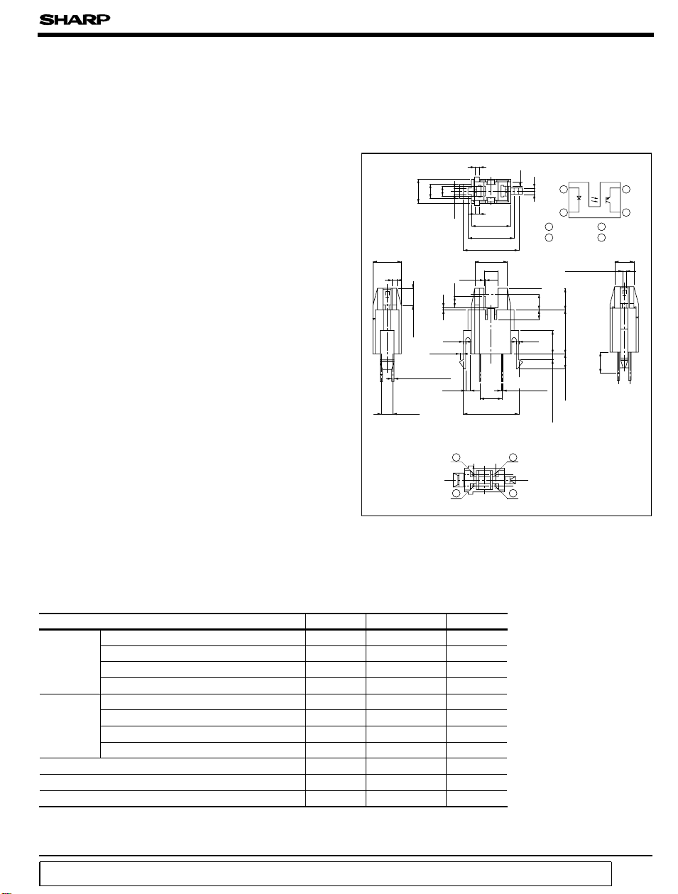
■ Outline Dimentions
1
3
2.2
6.2
1
4 - 0.45
(
2.54
4 - 3.8
5.2
+0.4
2 - 0.8
+0.3
- 0.2
)
1
1.5
+0.1
8.4
- 0.2
10
12
7 ± 0.3
3
0.3
- 0.2
2.4
0.5
0.5
2 - 1
(
)
4.75
+0.3
12
- 0.4
(
Top of Hook
23
(
Unit : mm
Internal connection diagram
1
1.5
1
23
1 Anode
2 Cathode
)
)
Center of
3.4
(
(
sensor
2.1
0.6
2 - 5
+ 0.3
4 - 0.25
- 0.2
2 - 1.4
)
* Unspecified tolerance :± 0.2mm
* ( ): Reference dimensions
* Please be careful not to receive
external disturbing light because
the top and back face of emitter
41
and detector elements are not
covered by case.
2-0.8
(
Slit width
0.3
-
+ 0.2
4.7
9.6
2 - 3.4
4 Collector
3 Emitter
±
0.1
0.1
)
MIN.4.5
)
4
4.2
■ Absolute Maximum Ratings
(
Ta= 25˚C
)
Parameter Symbol Rating Unit
Input
Forward current I
*1
Peak forward current I
Reverse voltage V
F
FM
R
50 mA
1A
6V
Power dissipation P 75 mW
Output
Collecotr-emitter voltage V
Emitter-collector voltage V
Collector current I
Collector power dissipation P
Operating temperature
Storage temperature T
*2
Soldering temperature T
CEO
ECO
C
C
T
opr
stg
sol
*1 Pulse width<=100 µs, Duty ratio: 0.01
*2 For 5 seconds
“ In the absence of confirmation by device specification sheets, SHARP takes no responsibility for any defects that occur in equipment using any of SHARP's devices, shown in catalogs,
data books, etc. Contact SHARP in order to obtain the latest version of the device specification sheets before using any SHARP's device.”
35 V
6V
20 mA
75 mW
- 25 to + 85
- 40 to + 100
˚C
˚C
260 ˚C
GP1S562
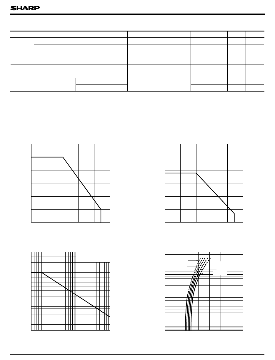
■ Electro-optical Characteristics
Parameter Symbol Condition MIN. TYP. MAX. Unit
Forward voltage V
Input
Output I
Transfer
characteristics
Fig. 1 Forward Current vs.
Ambient Temperature
)
mA
(
Peak forward voltage V
Reverse current I
Collector dark current
Collector current I
Collector-emitter saturation voltage
Response time
60
50
40
F
30
Rise time t
Fall time t
V
FM
R
CEO
C
CE(sat
r
f
(
Ta= 25˚C
F
IF= 20mA - 1.25 1.4 V
I
FM
= 0.5A
-34V
)
VR=3V - - 10 µA
VCE= 20V - 1 100 nA
VCE= 5V, IF= 20mA 1.4 - 8.5 mA
)
IF= 40mA, IC= 1.4mA - - 0.4 V
VCE= 2V, IC= 2mA
= 100Ω
R
L
-315
-420
µ s
µ s
Fig. 2 Collector Power Dissipation vs.
Ambient Temperature
120
)
100
mW
(
C
80
75
60
20
Forward current I
10
0
- 25 0 25 50 75 85 100
Ambient temperature Ta (˚C
Fig. 3 Peak Forward Current vs.
Duty Ratio
Pulse width<=100µ s
10
Duty ratio
Ta= 25˚C
-1
2000
)
1000
mA
(
FM
500
200
100
Peak forward current I
50
20
-2
52525
10
40
20
Collector power dissipation P
15
0
- 25 0 25 50 75 85 100
)
Ambient temperature Ta (˚C
)
Fig. 4 Forward Current vs. Forward Voltage
500
= 75˚C
T
a
200
100
)
mA
50
(
F
20
10
Forward current I
1
50˚C
5
2
010.5 1.0 1.5 2.0 2.5 3.0 3.5
Forward voltage VF (V
-
25˚C
0˚C
20˚C
)
 Loading...