

Page 1

SERVICE MANUAL
No. 00ZFO8MKU/SME
FACSIMILE
OPTION MEMORY
UPGRADE PWB
FO-8MK
MODEL
This machine is an Option Memory Unit applicable to
the FO-4400 Series.
CONTENTS
[1] General description . . . . . . . . . . . . . . . . . . . . . . . . . . . . . . . . . . . . . . . . . . . . . . . . 1
[2] Installation procedure . . . . . . . . . . . . . . . . . . . . . . . . . . . . . . . . . . . . . . . . . . . . . . . 1
[3] Diagnostic mode . . . . . . . . . . . . . . . . . . . . . . . . . . . . . . . . . . . . . . . . . . . . . . . . . . 1
[4] Circuit schematics and parts layout . . . . . . . . . . . . . . . . . . . . . . . . . . . . . . . . . . . . 3
FO-8MK
Parts guide
SHARP CORPORATION
This document has been published to be used
for after sales service only.
The contents are subject to change without notice.
Page 2
FO-8MK
[1] General description
This machine is an Option Memory Unit applicable to the FO-4400 Series. It enhances the memory-aided functions such as sequential simultaneous sending and through-memory substitute reception of facsimile.
[2] Installation procedure
(Pay attention to static electricity)
To install the Option Memory Unit, check the following in advance.
1) Make sure that the remaining memory capacity is 0%.
If the remaining memory capacity is not 0%, this implies that any data
remains in the image memory on the Control PWB.
2) Check that a sufficient quantity of paper exists. If there is no paper or
paper is lacking, replenish the machine with paper, and print the data
received and stored in the memory.
3) Then, check whether there is any confidentially received information,
seeing the confidential reception data list ("MENU" + "2" + "0" + "9").
If any confidentially received information is found, input the ID No. of
specific reception box, and print the confidentially received information.
4) After that, check whether there is timer sending information, seeing
the timer sending information list ("MENU" + "2" + "0" + "2"). It is
required to teach users that any timer sending information, if exists,
is cleared after the Option Memory Unit is installed and, accordingly,
users have to set again the timer sending and do the timer sending.
Install the Option Memory Unit in the following procedure.
1) Remove the Rear Cabinet of facsimile.
2) Loose two screws on the Standard Memory PWB and remove two
spacers. Then, remove the Standard Memory PWB from two locking
spacers and the connector.
3) Connect the Option Memory PWB to the connector CNOP1 of Control PWB and insert two locking spacers into the holes on the board.
Then, tighten two screws with each spacers. (Fig. 1)
4) Mount the Rear Cabinet.
5) After installation turn on power switch with pressing "ST ART" + "ST OP"
key.
[3] Diagnostic mode
Successively input "MENU" + "9" + " " + "8" + "#" + "7". Then, appears.
MAIN
:TA68
After that, press the "START" key.
Then, appears.
A:
SOFT SWITCH MODE
PRESS START KEY
Select the Flash Memory Test, using the key "L".
L:
FLASH MEMORY
PRESS START KEY
In the diagnostic mode perform the Image Memory (Standard, Option)
write/read test, as well as complete erase test.
When the "START" key is pressed,
S ––E
TEST EXECUTING
appears, and the indication changes from "–" to "■" whenever data is
written in the Flash Memory.
After completion of writing of data in all Flash Memories, the following
indication appears.
S
E
TEST EXECUTING
After that the long-tone buzzer (normal end) sounds, and at the same
time the following indication appears.
M:
ALL ENTRYFAX/TEL
PRESS START KEY
( is ROM
version.)
MEMORY CLEAR?
1=ALL, 2=IMAGE, 3=NO
appears.
Then, press "1" key to perform "ALL" clear.
PLEASE WAI T A MOMENT
appears.
Then, after several seconds,
SEP
M:00% STAND BY AUTO
26 TUE AM10:47
appears.
• The data initially registered will be deleted by this operation.
– 1 –
Page 3
FO-8MK
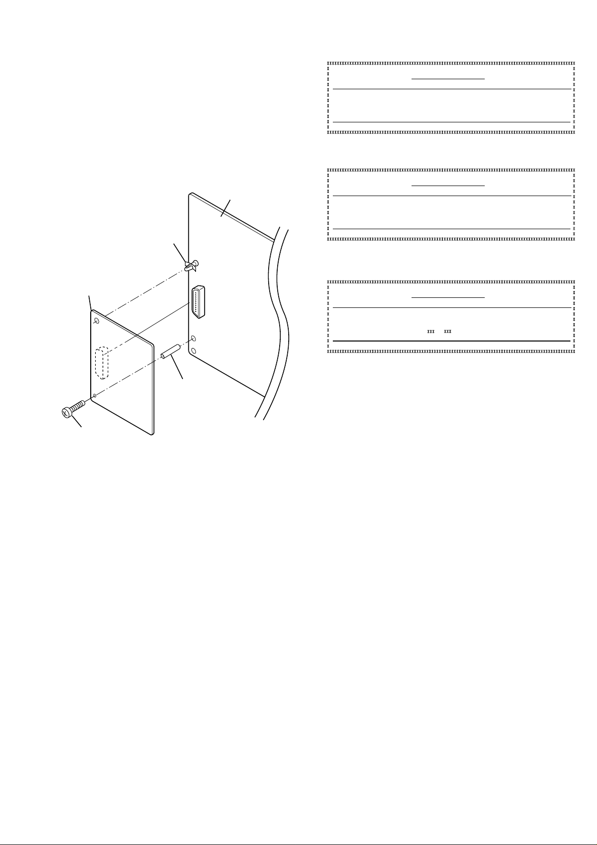
Then, the result table (Fig. 2) is printed.
In case of mismatch, the buzzer emits 3 long tones.
After that, the result table (Fig. 3) or (Fig.4) is output.
1) If any error occurred, check connection of connector CNOP1 (check
for bending and breakage of pin of connector), check that the Option
Memory Unit has been mounted as specified, and then turn on again
the power supply, and check.
2) If the same error occurs persistently after the measures stated in item
1 above were taken, replace the Option Memory Unit, and check.
3) If the same error occurs again after the measures stated in item 2)
were taken, check the Control PWB.
CONTROL PWB
PWB
Spacer
OPTION
MEMORY
PWB UNIT
FO-8MK
CNOP1
FLASH MEMORY CHECK LIST
NOR-FLASH = OK
NAND-FLASH STANDARD = OK [ 2MB]
OPTION = OK [ 8MB]
Fig. 2
FLASH MEMORY CHECK LIST
NOR-FLASH = OK
NAND-FLASH STANDARD = OK [ 2MB]
Fig. 3
FLASH MEMORY CHECK LIST
NOR-FLASH = OK
NAND-FLASH STANDARD = OK [ 2MB]
OPTION = NG [ 8MB]
OCT–08–2002 TUE 06:41 PM
OCT–08–2002 TUE 06:36 PM
OCT–08–2002 TUE 07:25 PM
CNOP
Screw
(3 x 25 mm)
Fig. 4
PWB
Support
Fig. 1
– 2 –
Page 4
FO-8MK
(1-2A)
(1-3A)
(1-3E)
(1-5B)
(1-6A)
(1-5B)
(1-5E)
(1-3A)
(1-3E)
(1-3E)
(1-3E)
(1-3E)
(1-3E)
(1-3E)
(1-5E)
(1-5E)
(1-5E)
(1-5E)
(1-5E)
(1-5E)
IO[7:0]
OPD2
OPD6
OPD4
OPD3
OPD3
OPD0
OPD6
OPD0
OPD7
OPD5
OPD1
OPD5
OPD4
OPD7
OPD1
OPD2
IO2
IO1
IO6
IO1
IO3
IO0
IO7
IO5
IO6
IO7
IO1
IO6
IO4
IO0
IO3
IO7
IO2
IO4
IO4
IO0
IO5
IO5
IO2
IO3
VCC
20
A12A2
3
A3
4
A45A5
6
A6
7
A78A8
9
B118B2
17
B3
16
B415B5
14
B613B7
12
B8
11
GND
10
DIR1OE
19
DG
1
DG
3
DG
5
+3.3V
7
+3.3V
9
+3.3V
11
RD/WR
13
OPDEN
15
OPD6
17
OPD4
19
OPD2
21
OPD0
23
DG
25
DG
27
DG
29
CLEO
2
ALEO
4
WP1
6
NANDWR
8
OPCS
10
BUSYOP
12
NANDRD
14
OPD7
16
OPD5
18
OPD3
20
OPD1
22
MEMDTC0
24
MEMDTC1
26
DG
28
DG
30
I/O827I/O726I/O6
25
I/O5
24
I/O421I/O3
20
I/O219I/O1
18
CLE2ALE
3
CE
43
WE
4
RE42WP
5
RY/BY
41
NC
28
GND
40
Vss
22
Vss
1
Vcc23Vcc
44
NC29NC30NC
31
NC
32
NC
13
NC
14
NC15NC
16
NC
17
NC
6
NC7NC
8
NC9NC
10
NC35NC
36
NC
37
NC38NC
39
I/O8
44
I/O7
43
I/O6
42
I/O541I/O4
32
I/O331I/O2
30
I/O1
29
CLE
16
ALE17CE
9
WE18RE
8
WP
19
RY/BY
7
NC
26
GND
6
Vss
36
Vss
13
Vcc
12
Vcc
37
NC
27
NC
28
NC33NC
34
NC
21
NC22NC
23
NC24NC
25
NC
1
NC2NC
3
NC
4
NC
5
NC
35
NC
40
NC
47
NC
38
NC
39
NC
10
NC11NC
14
NC
15
NC
20
NC
45
NC
46
NC
48
C18
0.1u
C4
N.M.
+
TP3
C1
22u/16V
+C16
0.1u
TP4
C13
0.1u
IC2
C12
0.1u
TP9
TP5
RA1
0x4
TP7
C2
22u/16V
+
CNOP
DHB-RD30-S131N-2.9
1357911131517192123252729
20
18
16
141210
864
2
30
28
26
24
22
TP6
TP1
C10
0.1u
IC1
TC58V64BFT
R12
N.M.
R10 0
TP8
RA3
TP10
R11
N.M.
C11
N.M.
TP11
C3
22u/16V
+
C15
R13 0
RA4
IC3
C14
C17
N.M.
TP2
R14
2.2k
RA2
0x4
+3.3V
+3.3V
DG
DG
+3.3V
DG
DG
DG
+3.3V
DG
DG
DG
DG
+3.3V
+3.3V
CLEO
ALEO
/OPCS
/NANDWR
/NANDRD
/WP1
/BUSYOP
OPD[7:0]
/OPDEN
RD/WR
RD/WR
/OPDEN
OPD[7:0]
/WP1
CLEO
/BUSYOP
/NANDWR
ALEO
/NANDRD
/OPCS
A
A
B
B
C
C
D
D
E
E
F
F
G
G
H
H
I
I
6 6
5 5
4 4
3 3
2 2
1 1
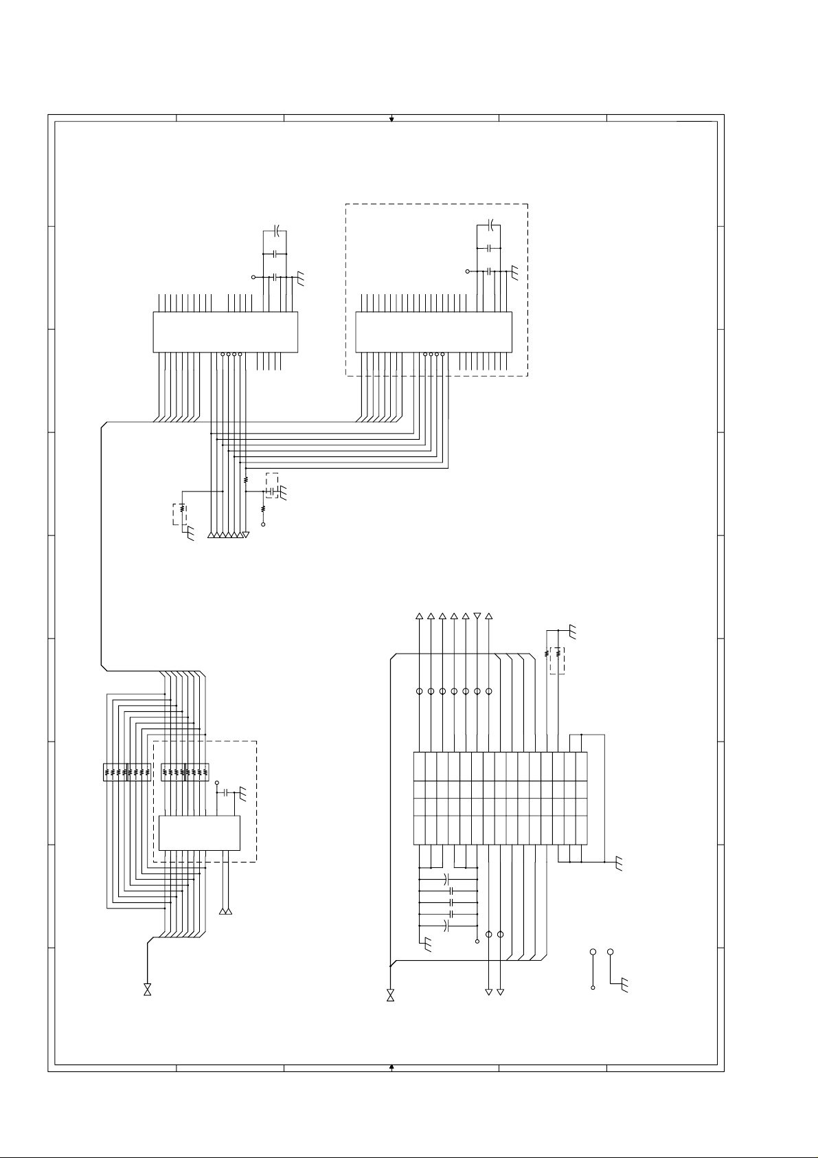
[4] Circuit schematics and parts layout
Option Memory PWB circuit 1/1
– 3 –
Page 5
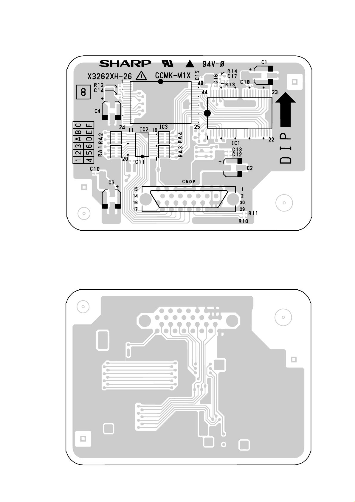
Option Memory PWB parts layout (Top side)
FO-8MK
Option Memory PWB parts layout (Bottom side)
– 4 –
Page 6

FO-8MK
PARTS GUIDE
MODEL FO-8MK
CONTENTS
1 Packing Parts
2 Option Memory PWB Unit
NO.
PARTS CODE
PRICE
RANK
NEW
MARK
PART
RANK
DESCRIPTION
[1] Packing parts
1 LSTY-0057AFZZ AC C PWB spacer
2 PSHEM3490XHZZ AC C Aluminum fold
3 SPAKC210EXHTZ AE N D Packing case
4 PCAPZ2030XHZZ AF C PWB support
5 XHPSD30P25000 AA C Screw(3x25)
[2] Option memory PWB unit
1 VCEAPS226AF1C AC C Capacitor(16WV 22µF) [C1]
2 VCEAPS226AF1C AC C Capacitor(16WV 22µF) [C2]
3 VCEAPS226AF1C AC C Capacitor(16WV 22µF) [C3]
4 VCKYCZ1CF104Z AB C Capacitor(16WV 0.1µF) [C10]
5 VCKYCZ1CF104Z AB C Capacitor(16WV 0.1µF) [C12]
6 VCKYCZ1CF104Z AB C Capacitor(16WV 0.1µF) [C13]
7 VCKYCZ1CF104Z AB C Capacitor(16WV 0.1µF) [C16]
8 VCKYCZ1CF104Z AB C Capacitor(16WV 0.1µF) [C18]
9 QCNCW2590SC3J AS N C Connector(30pin) [CNOP]
10 RH-IX2298XHZZ BK N B IC(TC58V64BFT) [IC1]
11 VRS-CZ1JB000J AA C Resistor(1/16W 0Ω ±5%) [R10]
12 VRS-CZ1JB000J AA C Resistor(1/16W 0Ω ±5%) [R13]
13 VRS-CZ1JB222J AD C Resistor(1/16W 2.2KΩ ±5%) [R14]
14 RR-TZ3021SCZZ AF B Block resistor(0Ωx4) [RA1]
15 RR-TZ3021SCZZ AF B Block resistor(0Ωx4) [RA2]
901 DCEKM433CXH01 BA N E Option memory PWB unit
(Unit)
COPYRIGHT © 2002 BY SHARP CORPORATION
ALL RIGHTS RESERVED.
No part of this publication may be reproduced,
stored in a retrieval system, or transmitted in
any form or by any means, electronic, mechanical,
photocopying, recording, or otherwise, without
prior written permission of the publisher.
SHARP CORPORATION
Communication Systems Group
Quality & Reliability Control Center
Higashihiroshima, Hiroshima 739-0192, Japan
Printed in U.S.A.
A0211-1100DS•IS•T
 Loading...