

Page 1
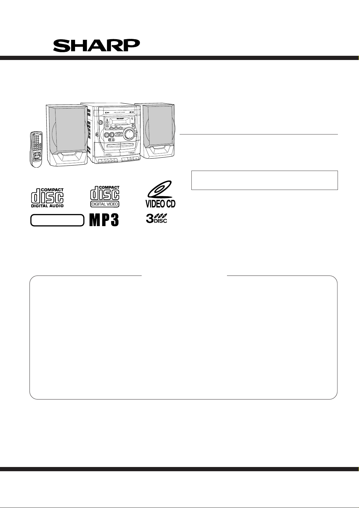
CD-XP125V
SERVICE MANUAL
No. SY296CDXP125V
VIDEO CD MINI SYSTEM
MODEL CD-XP125V
CD-XP125V Video CD Mini System consisting of CD-XP125V
(main unit) and CP-XP125 (speaker system).
• In the interests of user-safety the set should be restored to its
original condition and only parts identical to those specified be
used.
NTSC/PAL
CONTENTS
Page
SAFETY PRECAUTION FOR SERVICE MANUAL ........................................................................................................... 2
VOLTAGE SELECTION..................................................................................................................................................... 2
AC POWER SUPPLY CORD
SPECIFICATIONS ............................................................................................................................................................. 3
NAMES OF PARTS ........................................................................................................................................................... 4
DISASSEMBLY.................................................................................................................................................................. 6
REMOVING AND REINSTALLING THE MAIN PARTS..................................................................................................... 8
ADJUSTMENT ................................................................................................................................................................. 10
TEST MODE .................................................................................................................................................................... 13
NOTES ON SCHEMATIC DIAGRAM .............................................................................................................................. 15
TYPES OF TRANSISTOR AND LED............................................................................................................................... 15
BLOCK DIAGRAM ........................................................................................................................................................... 16
SCHEMATIC DIAGRAM / WIRING SIDE OF P.W.BOARD............................................................................................. 22
VOLTAGE ........................................................................................................................................................................ 45
FUNCTION TABLE OF IC................................................................................................................................................ 46
FL DISPLAY..................................................................................................................................................................... 56
REPLACEMENT PARTS LIST/EXPLODED VIEW
AND AC PLUG ADAPTOR ................................................................................................. 2
SHARP CORPORATION
This document has been published to be used
for after sales service only.
The contents are subject to change without notice.
Page 2
CD-XP125V
SAFETY PRECAUTION FOR SERVICE MANUAL
WARNINGS
THE AEL (ACCESSIBLE EMISSION LEVEL) OF THE LASER POWER OUTPUT IS LESS THAN CLASS 1 BUT THE LASER
COMPONENT IS CAPABLE OF EMITTING RADIATION EXCEEDING THE LIMIT FOR CLASS 1. THEREFORE IT IS
IMPORTANT THAT THE FOLLOWING PRECAUTIONS ARE OBSERVED DURING SERVICING TO PROTECT YOUR EYES
AGAINST EXPOSURE TO THE LASER BEAM.
1-WHEN THE CABINET IS REMOVED, THE POWER IS TURNED ON WITHOUT A COMPACT DISC IN POSITION AND THE
PICKUP IS ON THE OUTER EDGE THE LASER WILL LIGHT FOR SEVERAL SECONDS TO DETECT A DISC. DO NOT
LOOK INTO THE PICKUP LENS.
2-THE LASER POWER OUTPUT OF THE PICKUP UNIT AND REPLACEMENT SERVICE PARTS ARE ALL FACTORY
PRESET BEFORE SHIPMENT.
DO NOT ATTEMPT TO READJUST THE LASER PICKUP UNIT DURING REPLACEMENT OR SERVICING.
3-UNDER NO CIRCUMSTANCES STARE INTO THE PICKUP LENS AT ANY TIME.
4-CAUTION-USE OF CONTROLS OR ADJUSTMENTS, OR PERFORMANCE OF PROCEDURES OTHER THAN THOSE
SPECIFIED HEREIN MAY RESULT IN HAZARDOUS RADIATION EXPOSURE.
Laser Diode Properties
Material: GaAIAs
Wavelength: 780 nm
Emission Duration: continuous
Laser Output: max. 0.6 mW
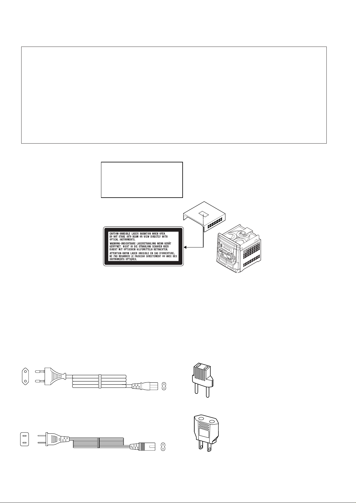
VOLTAGE SELECTION
Before operating the unit on mains, check the preset voltage. If the voltage is different from your local voltage, adjust the voltage
as follows.
Turn the selector with a screwdriver until the appropriate voltage number appears in the window (110 V, 127 V, 220 V or 230 V - 240 V AC).
AC POWER SUPPLY CORD AND AC PLUG ADAPTOR
QACCE0002SJ00
QACCA0002SJ00
QPLGA0250AFZZ
QPLGA0253AFZZ
– 2 –
Page 3
CD-XP125V
CD-XP125V
FOR A COMPLETE DESCRIPTION OF THE OPERATION OF THIS UNIT, PLEASE REFER
TO THE OPERATION MANUAL.
SPECIFICA TIONS
General
Power source AC 110/127/220/230 - 240 V, 50/60 Hz
Power
consumption
Dimensions Width: 270 mm (10-5/8")
Weight 6.9 kg (15.2 lbs.)
66 W
Height: 305 mm (12")
Depth: 343 mm (13-1/2")
Amplifier
Output power MPO: 60 W (30 W + 30 W) (10 % T.H.D.)
RMS: 40 W (20 W + 20 W) (10 % T.H.D.)
RMS: 30 W (15 W + 15 W) (0.9 % T.H.D.)
Output terminals Speakers: 8 ohms
Headphones: 16 - 50 ohms (recommended:
32 ohms)
Video out: 1 Vp-p (75 ohms)
Input terminals Microphone: 1 mV/600 ohms
Video CD
Video output
format
Specifications for this model are subject to change without
prior notice.
PAL/NTSC
CD player
Type 3-disc multi-play compact disc player
Signal readout Non-contact, 3-beam semiconductor laser
D/A converter 1-bit D/A converter
Frequency
response
Dynamic range 90 dB (1 kHz)
pickup
20 - 20,000 Hz
Tuner
Frequency range FM: 88 - 108 MHz
AM: 531 - 1,602 kHz
Cassette deck
Frequency
response
Signal/noise ratio 50 dB (TAPE 1, recording/playback)
Wow and flutter 0.3 % (WRMS)
CP-XP125
Type 2-way type speaker system
Tweeter
Maximum input
power
Rated input power 20 W
Impedance 8 ohms
Dimensions Width: 200 mm (7-7/8")
Weight 2.4 kg (5.3 lbs.)/each
125 - 8,000 Hz (Normal tape)
50 dB (TAPE 2, playback)
10 cm (4") Woofer
40 W
Height: 305 mm (12")
Depth: 167 mm (6-9/16")
– 3 –
Page 4
CD-XP125V
NAMES OF P ARTS
CD-XP125V
Front panel
1. Disc Tray
2. Timer Set Indicator
3. Video CD Playback Control Button
4. Video CD On Screen Display On/Off Button
5. On/Stand-by Button
6. Video CD Digest/Time Search Button
7. Video CD Skip or Previous,
CD/MP3 Disc Track Down or
Fast Reverse, Tuner Preset Down Button
8. Headphone Socket
9. Video CD Stop or Return,
CD/MP3 Disc Stop Button
10. Video CD/CD/MP3 Disc Play or Repeat Button
11. Microphone Level Control
12. Microphone Socket
13. Tape 1 Cassette Compartment
14. Video CD/CD/MP3 Disc Button
15. Tuner (Band) Button
16. Tape Button
17. Video CD Skip or Next, CD/MP3 Disc Track Up or
Fast Forward, Tuner Preset Up Button
18. Equaliser Mode Select/Extra Bass/
Demo Mode Button
19. Disc Tray Open/Close Button
20. Disc Skip Button
21. Volume Up and Down Buttons
22. Tuning Up Button
23. Tuning Down Button
24. Tape 2 Cassette Compartment
25. Tape 1 Record Button
26. Tape 1 Play Button
27. Tape 1 Rewind Button
28. Tape 1 Fast Forward Button
29. Tape 1 Stop/Eject Button
30. Tape 1 Pause Button
31. Tape 2 Play Button
32. Tape 2 Rewind Button
33. Tape 2 Fast Forward Button
34. Tape 2 Stop/Eject Button
10
11
12
13
1
2
3
4
14
15
16
5
6
7
8
9
17
18
19
20
21
22
23
24
25
26 27 28 29 30 31 32 33 34
Display
1. Disc Play Indicator
2. Disc Repeat Play Indicator
3. FM Station Indicator
4. AM Station Indicator
5. Disc Number Indicators
6. Clock Indicator
7. Sleep Indicator
8. Timer Play Indicator
9. Tape 1 Record Indicator
10. Disc Pause Indicator
11. FM Stereo Mode Indicator
12. MP3 Disc Indicator
13. FM Stereo Receiving Indicator
14. Memory Indicator
15. Disc Random Play Indicator
16. Extra Bass Indicator
1 2 3 4 11 12 13
5
6
78910 16
14
15
– 4 –
Page 5
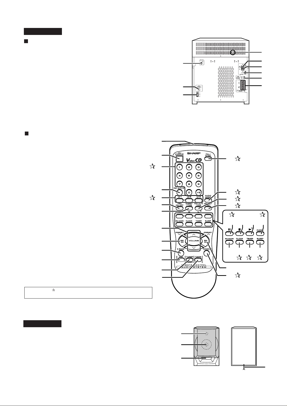
CD-XP125V
Rear panel
CD-XP125V
1. Video Output Socket
2. AC Voltage Selector
3. AC Power Input Socket
4. Transport Screw
5. FM 75 Ohms Aerial Terminal
6. FM Aerial Earth Terminal
7. AM Loop Aerial Socket
8. Span Selector Switch
9. Speaker Terminals
Remote control
1. Remote Control Transmitter
2. On/Stand-by Button
3. Disc Direct Search Buttons
4. Video CD Playback Control Auto/Off Button
5. Disc Number Select Buttons
6. Video CD On Screen Display On/Off Button
7. Video CD Digest/Time Search Button
8. Volume Up and Down Buttons
9. Video CD Skip or Previous, CD/MP3 Disc Track Down or
Fast Reverse, Tuner Preset Down Button
10. Extra Bass Button
11. Video CD/CD/MP3 Disc Button
12. Tuner (Band) Button
13. Tape Button
14. PAL/NTSC Select Button
15. Audio Mode Button
16. Video CD Auto/On Button
17. Memory/Set Button
18. Video CD Skip or Next, CD/MP3 Disc Track Up or
Fast Forward, Tuner Preset Up Button
19. Disc Random Button
20. Disc Pause Button
21. Video CD Stop or Return, CD/MP3 Disc Stop Button
22. Video CD/CD/MP3 Disc Play or Repeat Button
23. Clear Button
24. Equaliser Mode Select Button
25. Clock Button
26. Timer Button
27. Sleep Button
10
11
12
13
4
1
5
6
7
8
2
9
3
1
2
14
3
4
5
6
15
16
17
7
20
21 22 23
8
9
24 25 26 27
18
19
Buttons with " "mark in the illustration can be operated on the remote control only.
CP-XP125
1. Tweeter
2. Woofer
3. Bass Reflex Duct
4. Speaker Wire
– 5 –
1
2
3
4
Page 6
CD-XP125V
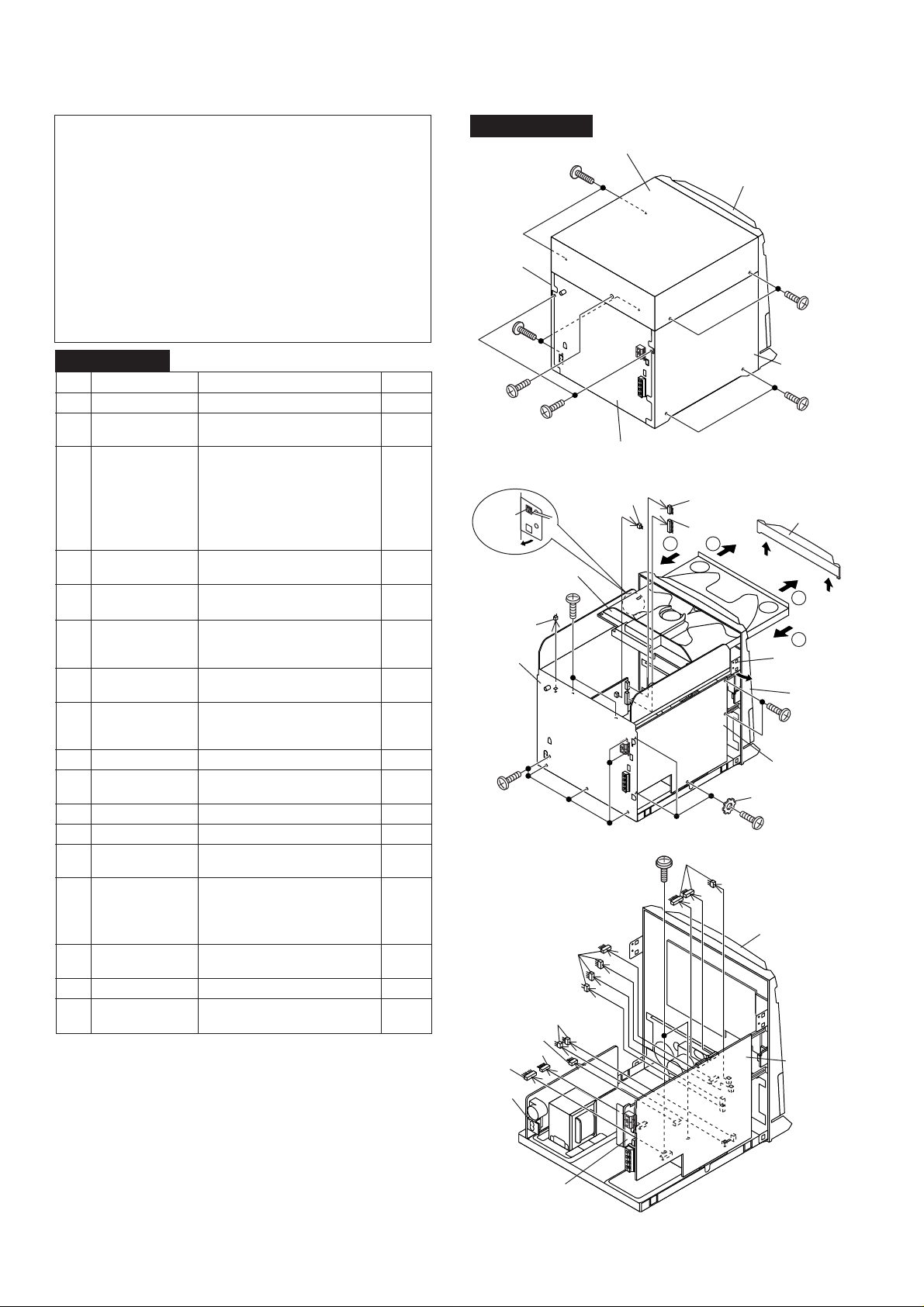
DISASSEMBLY
Caution on Disassembly
Follow the below-mentioned notes when disassembling
the unit and reassembling it, to keep it safe and ensure
excellent performance:
1. Take cassette tape and compact disc out of the unit.
2. Be sure to remove the power supply plug from the wall
outlet before starting to disassemble the unit.
3. Take off nylon bands or wire holders where they need to
be removed when disassembling the unit. After servicing
the unit, be sure to rearrange the leads where they were
before disassembling.
4. Take sufficient care on static electricity of integrated
circuits and other circuits when servicing.
CD-XP125V
Side Panel
(Right)
(B1)x2
ø3x10mm
(A1)x2
ø3x16mm
Top Cabinet
Front
Panel
(A1)x2
ø3x16mm
CD-XP125V
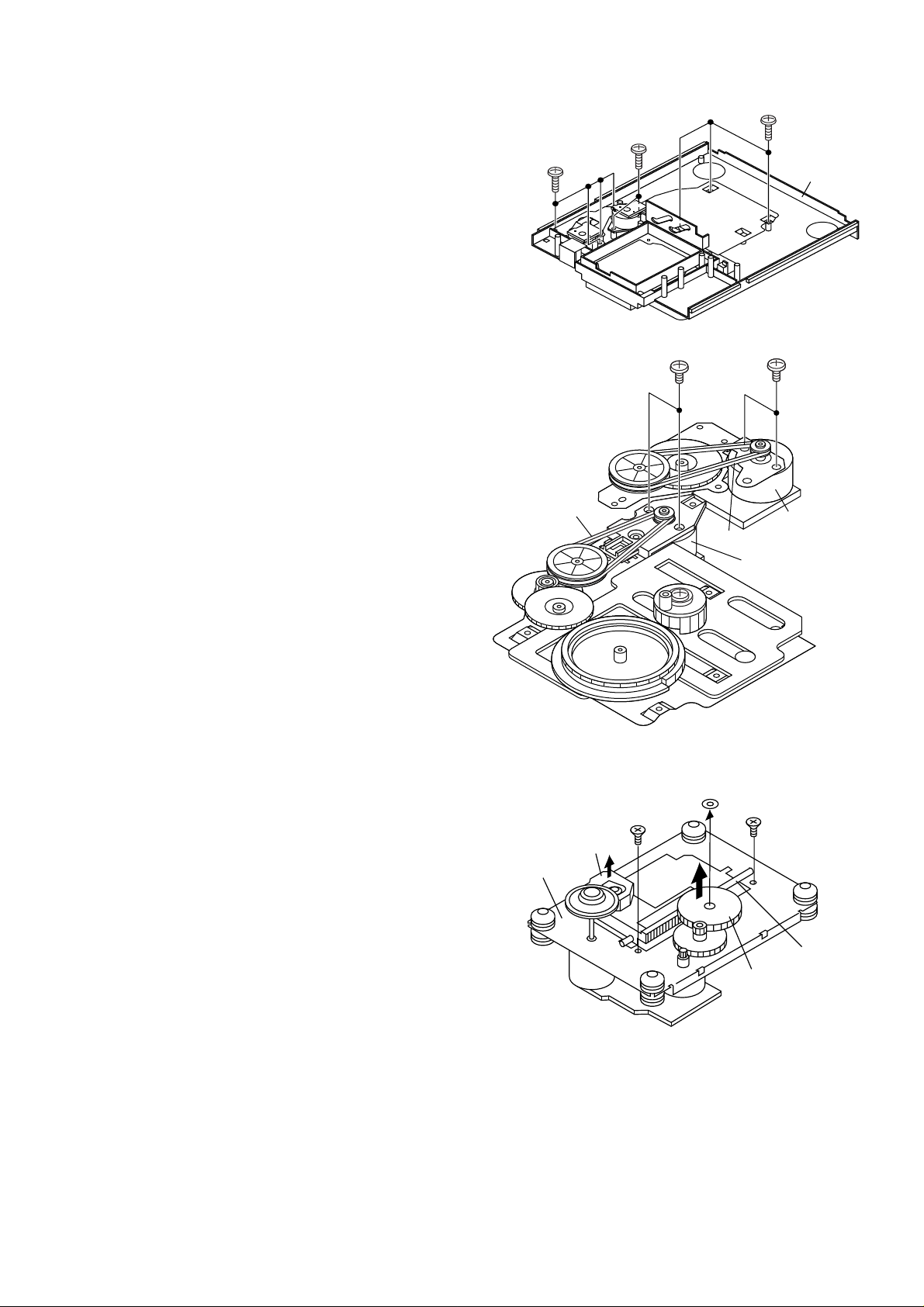
STEP
10 Tape Mechanism 1. Open the cassette holder. 7-2
11
12
13 Turntable 1. Screw ...................... (N1) x1 7-3
14 Loading Tray 1.
15 CD Servo PWB 1. Screw ...................... (Q1) x3 7-4
16 Switch B PWB 1. Screw ...................... (R1) x2 7-4
17 CD Mechanism 1. Screw ...................... (S1) x4 7-5
Note 1:
1. After removing the connector for the optical pickup from the
REMOVAL PROCEDURE FIGURE
1 Top Cabinet 1. Screw ...................... (A1) x5 6-1
2 Side Panel 1. Screw ...................... (B1) x6 6-1
(Left/Right)
3 CD Player Unit 1. Turn on the power supply, .. 6-2
4 Rear Panel With 1. Screw ...................... (D1) x6 6-2
Video Out PWB 2. Socket ..................... (D2) x1
5 Main PWB 1. Screw ...................... (E1) x7 6-2,6-3
6 Front Panel 1. Screw .......................(F1) x3 7-1
7 Switch A PWB 1. Screw ...................... (G1) x3 7-2
8 Decode PWB 1. Screw ...................... (H1) x2 7-1
9 Display PWB 1. Screw .....................(J1) x10 7-2
Headphones PWB
Mic PWB
(Note 1) 2. Socket ..................... (Q2) x5
connector, wrap the conductive aluminium foil around the front end
of the connector so as to protect the optical pickup from electrostatic damage.
open the disc tray, take out
the CD tray cover, and close.
2. CD Tray Cover........ (C1) x1
4. Screw ...................... (C2) x2
3. Hook........................ (C3) x2
4. Socket ..................... (C4) x3
2. Socket ................... (E2) x11 6-3
2. Hook.........................(F2) x2
3. Socket ......................(F3) x1 6-3
2. Socket ..................... (G2) x1
2. Socket ..................... (H2) x1
3. Flat Cable ............... (H3) x1
2. Screw...................... (K1) x8
1. Screw ........................ L1) x1 7-2
1. Screw ......................(M1) x2 7-2
2. Spacer..................... (N2) x1
Push forward the loading tray.
2.
Inserting the flat head into the
hole, push in the direction indi-
cated by the arrow. ...
2. Spring...................... (S2) x4
(P1) x2
7-3
(A1)x1
ø3x8mm
(C3)x1
Pull
(D2)x1
Rear
Panel
(D1)x6
ø3x8mm
(E2)x1
(F3)x1
(E2)x1
Power
PWB
(B1)x2
ø3x8mm
CD Player
Unit
(C2)x2
ø3x5mm
(E2)x2
(E2)x4
Rear
Panel
Figure 6-1
(C4)x1
Figure 6-2
(E1)x2
ø3x10mm
2
(E2)x3
(C4)x1
(C4)x1
1
Side Panel
(Left)
(B1)x2
ø3x10mm
(C3)x1
Pull
(E1)x2
ø3x8mm
Main PWB
Washer
(E1)x3
ø3x10mm
Front
Panel
(C1)x1
1
2
Front
Panel
Main PWB
– 6 –
Decode PWB
Figure 6-3
Page 7
CD-XP125V
(F2)x1
Power
PWB
Decode PWB
Display PWB
(J1)x10
ø2.5x10mm
Tape
Mechanism
(K1)x8
ø3x10mm
(H1)x2
ø3x6mm
(H3)x1
(H2)x1
Figure 7-1
Front Panel
(F1)x3
ø3x6mm
(M1)x2
ø2.5x10mm
Switch A
PWB
Display PWB
Front
Panel
Mic
PWB
(F2)x1
(G2)x1
CD Servo
PWB
(Q2)x2
(S1)x4
ø2.5x8mm
(S2)x4
(Q1)x3
ø3x24mm
(Q2)x1
(Q2)x1
Figure 7-4
CD Mechanism
(Q2)x1
(R1)x2
ø3x8mm
Loading
Tray
Switch B
PWB
Loading Tray
(G1)x3
ø2.5x10mm
(L1)x1
ø2.5x10mm
Loading Tray
Headphones
PWB
(N1)x1
ø3x8mm
Washer
Turntable
Figure 7-2
(N2)x1
Open
Cassette
Holder
Screwdriver
(P1)x1
Screwdriver
(P1)x1
Figure 7-4
CP-XP125
This speaker CP-XP125 is available in assembles only and
may not be disassembled.
Figure 7-3
– 7 –
Page 8
CD-XP125V
REMOVING AND REINSTALLING THE MAIN PARTS
TAPE MECHANISM SECTION
Perform steps 1 to 6 and 10 of the disassembly method to
remove the tape mechanism.
How to remove the record/playback and erase
heads (TAPE 1) (See Fig. 8-1)
1. When you remove the screws (A1) x 2 pcs., the record/
playback head can be removed.
2. Move the hooks (A2) x 2 pcs., toward the center position as
shown in Fig. 8-1 and then lift the erase head.
Hook
(A2)x2
(A1)x1
ø2x7mm
(A1)x1
ø2x3mm
TAPE 1
Record/Playback
Head
How to remove the playback head (TAPE 2)
(See Fig. 8-2)
1. When you remove the screws (B1) x 2 pcs., the playback
head can be removed.
How to remove the pinch roller (TAPE 1)
(See Fig. 8-3)
1. When you remove the screw (C1) x 1 pc., the pinch roller
can be removed.
Note:
When installing the pinch roller, pay attention to the spring
mounting position.
How to remove the pinch roller (TAPE 2)
(See Fig. 8-3)
1. When you remove the screw (D1) x 1 pc., the pinch roller
can be removed.
Note:
When installing the pinch roller, pay attention to the spring
mounting position.
How to remove the tape motor (See Fig. 8-4)
1. Remove the belt.
2. Remove the screws (E1) x 6 pcs., to remove the motor
bracket.
3. Remove the screws (E2) x 3 pcs., to remove the tape motor.
Erase
Head
TAPE 1
(B1)x1
ø2x6mm
(C1)x1
ø2x4mm
Pinch Roller
Figure 8-1
(B1)x1
ø2x6mm
Figure 8-2
Playback
Head
TAPE 2
TAPE 2
(D1)x1
ø2x4mm
Pinch Roller
How to remove the belt (TAPE 1)
(See Fig. 8-5)
1. Remove the main belt (F1) x 1 pc., from the tape motor side.
2. Remove the FF/REW belt (F2) x 1 pc.
How to remove the belt (TAPE 2)
(See Fig. 8-5)
1. Remove the main belt (G1) x 1 pc., from the tape motor side.
2. Remove the FF/REW belt (G2) x 1 pc.
Tape
Motor
TAPE 2
Main
Belt
(G1)x1
REW/FF
Clutch Ass'y
REW/FF
Belt
(G2)x1
TAPE 2
Main Belt
(G1)x1
Main
Belt
(F1)x1
TAPE 1
Main Belt
(F1)x1
Tape
Motor
REW/FF
Belt
(F2)x1
TAPE 1
REW/FF
Clutch Ass'y
– 8 –
(E1)x2
ø2x4mm
Tape
Motor
Tape
Motor
Figure 8-3
(E1)x2
ø2x4mm
(E1)x2
ø2x4mm
Motor
Bracket
(E2)x3
Special Screw
Motor
Bracket
Figure 8-4Figure 8-5
Page 9
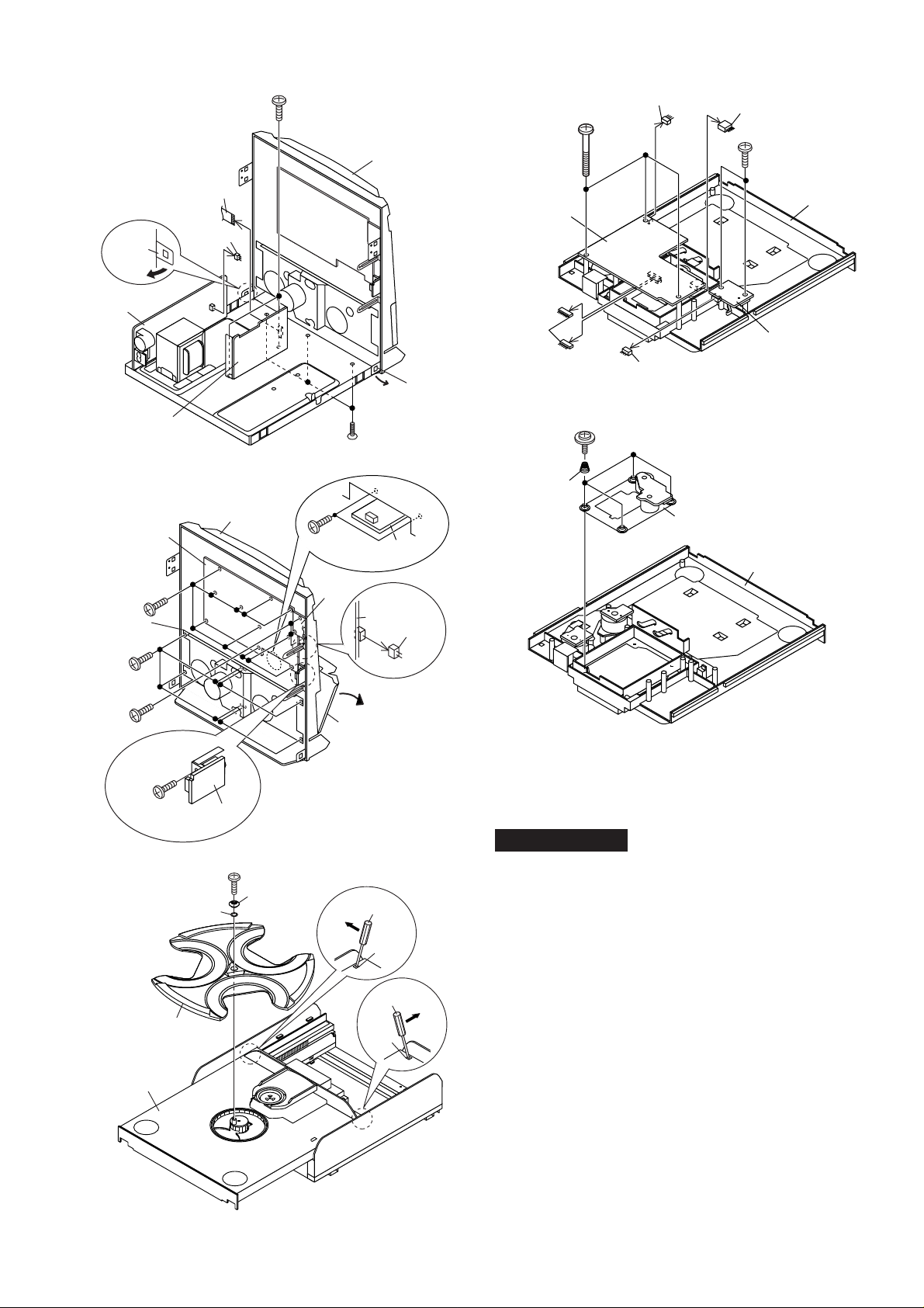
CD MECHANISM SECTION
(B1)x2
ø3x8mm
(A1)x4
ø3x8mm
(B1)x3
ø3x8mm
Loading
Tray
(B3)x2
ø2.4x3mm
(B2)x1
(A2)x1
Loading
Motor
T/T Up/Down
Motor
(A3)x2
ø2.4x3mm
Perform steps 1, 2, 3, 13, 14, 15 and 17 of the disassembly
method to remove the CD mechanism.
How to remove the T/T up/down motor
(See Figs. 9-1, 9-2)
1. Remove the screws (A1) x 4 pcs.
2. Remove the belt (A2) x 1 pc.
3. Remove the screws (A3) x 2 pcs., to remove the T/T up/
down motor.
CD-XP125V
Figure 9-1
How to remove the loading motor
(See Figs. 9-1, 9-2)
1. Remove the screws (B1) x 5 pcs.
2. Remove the belt (B2) x 1 pc.
3. Remove the screws (B3) x 2 pcs., to remove the loading
motor.
How to remove the pickup (See Fig. 9-3)
1. Remove the stop washer (C1) x 1 pc., to remove the gear
(C2) x 1 pc.
2. Remove the screws (C3) x 2 pcs., to remove the shaft
(C4) x 1 pc.
3. Remove the pickup.
Note
After removing the connector for the optical pickup from the
connector wrap the conductive aluminium foil around the front
end of connector so as to protect the optical pickup from
electrostatic damage.
CD
Pickup
Mechanism
(C3)x1
ø2.6x6mm
Figure 9-2
Stop Washer
(C1)x1
(C3)x1
ø2.6x6mm
Gear
(C2)x1
Shaft
(C4)x1
Figure 9-3
– 9 –
Page 10
CD-XP125V
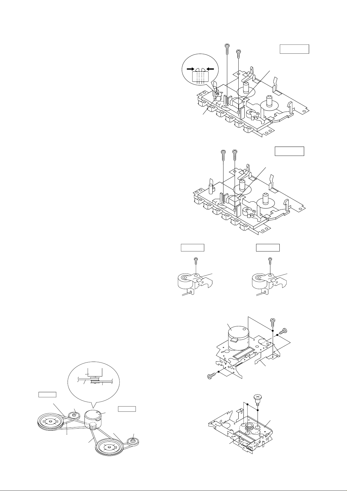
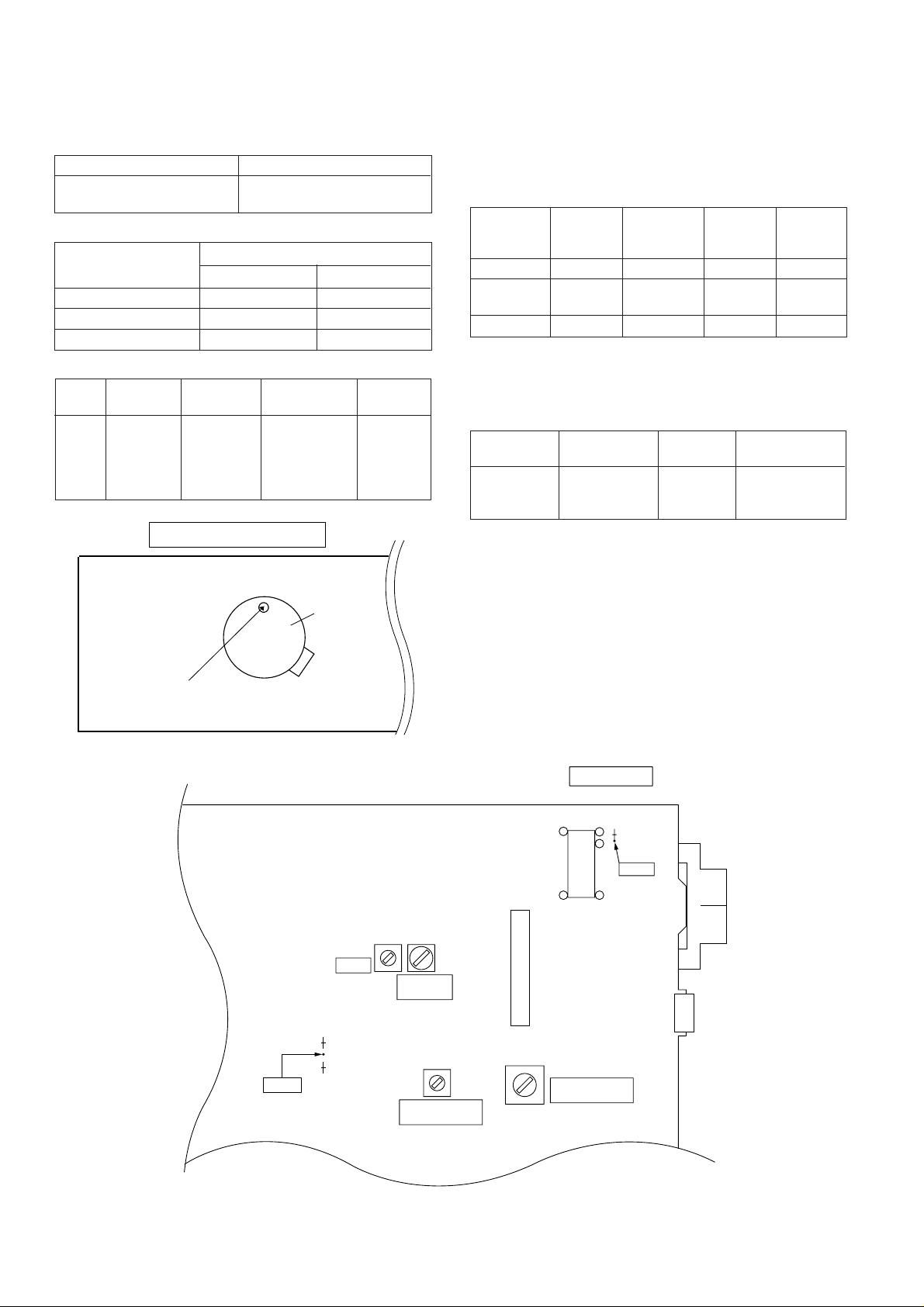
ADJUSTMENT
MECHANISM SECTION
••
• Driving Force Check
••
Torque Meter Specified Value
Play: TW-2111 Tape 1: Over 80 g
Tape 2: Over 80 g
••
• Torque Check
••
Torque Meter
Play: TW-2111 30 to 80 g.cm 30 to 80 g.cm
Fast forward: TW-2231 — 70 to 180 g.cm
Rewind: TW-2231 — 70 to 180 g.cm
••
• Tape Speed
••
Test Tape
Tape MTT-111 Variable 3,000 ± 30 Hz Speaker
speed Resistor in Terminal
Adjusting
Point
motor. (Load
TAPE MECHANISM
Specified Value
Tape 1
Specified
Value
Tape 2
Instrument
Connection
resistance:
6 ohms)
TUNER SECTION
fL: Low-range frequency
fH: High-range frequency
••
•
AM IF/RF
••
Signal generator: 400 Hz, 30%, AM modulated
Test Stage Frequency Frequency
AM IF 450 kHz 1,602 kHz T351 *1
AM Band — 531 kHz (fL): T306 *2
Coverage 1.1 ± 0.1 V
AM Tracking 990 kHz 990 kHz (fL): T302 *1
Display
*1. Input: Antenna Output: TP302
*2. Input: Antenna Output: TP301
• FM Mute Level (FM ST MODE)
Signal generator: 1 kHz, 40 kHz dev., FM modulated
Frequency
98.00 MHz 98.00 MHz VR351*1 Input: CNP301
(26 dBµV) Output: Speaker
Display
Adjusting
*1. Adjust so that an output signal appears.
Parts
Setting/
Adjusting
Parts
Connection
Terminal
Instrument
Connection
Instrument
Tape
Motor
Variable Resistor in motor
Figure 10-1
T351
AM IF
VR351
FM MUTE
Level
• FM IF
Notes:
1. Description of the "FM IF Adjustment" is not carried on this
Manual. It is because the IF coil in the FM front end section
has been best adjusted in the factory so that its further
adjustment is not needed at the field. When replacing the
FM front end assembly, no adjustment is needed either.
2. The parts in the FM front end section are prepared in a
complete unit, so you can't obtain each part individually.
MAIN PWB
1
22
R381
20
TP301
IC302
11 12
SO302
TERMINAL
FM ANTENNA
IC301
TP302
R356
R357
T306
AM BAND
COVERAGE fL
Figure 10-2 ADJUSTMENT POINTS
– 10 –
T302
AM TRACKING
fL
CNP301
Page 11
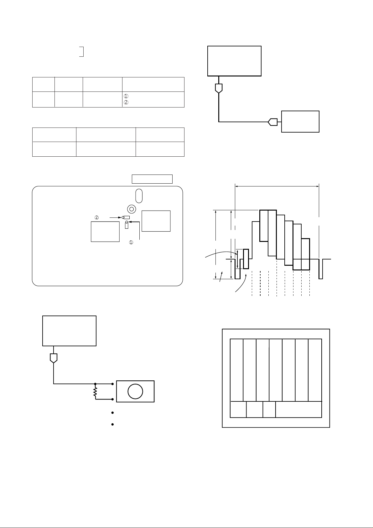
VIDEO CD SECTION
SET
Video Output Terminal
Video Input Terminal
TV
A-BEX
TEST VIDEO CD
••
• Measurement of oscillation frequency
••
Disc Adjusting
CD Stop TC100V 27.00000 MHz1 of R163V and
••
• Checking of video output signal
••
Point
Model No.
Instrument
Connection
± 160 Hz
Checking of color bar
Disc Adjusting Point
Track 2 Video output terminal Chroma Peak Level
TVD-581
TVD-581A
Specified Value
2
of C183V
Instrument
Connection
100 ± 15 IRE
CD-XP125V
Figure 11-3 Checking of video output signal
VIDEO PWB
X1
R163
1
PCLK2X
TC100
2
C183
GND
IC15
Figure 11-1 ADJUSTMENT POINTS
SET
VIideo Output Terminal
IC14
140 IRE
40 IRE
(1V)
(0.286V)
40 IRE
Color Burst
100 IRE
(0.714V)
-40
Gray
100 100
75
33.5
20
-20
Gray
Figure 11-4
Cyan
Yellow
(59.94Hz/NTSC)
IH
88.5
5
0
-13.5
Magenta
Cyan
Yellow
Green
75
Green
Magenta
Color bar signal
70
waveform
41.5
-25 -25
Blue
Red
Red
Blue
Horizontal
sync signal
75 ohms
Figure 11-2 Measurement of oscillation frequency
GND
Vectorscope
Waveform monitor
or oscilloscope
TV monitor
Figure 11-5
– 11 –
Page 12
CD-XP125V
Checking of vector scope waveform
Checking SettingDisc Checking
Track 2 VIDEO OUT Set the phase of Phase check
color burst signal ± 10°
(B) to 180°-360°
line.
Item
( Check that the setting is within the illustrated range.)
I
R-Y
R
MG
YL
75%
-Q
G
CY
-I
[NTSC] [PAL]
Checking the black-and-white level
Checking Checking ItemDisc
Track 16 VIDEO OUT Output level
100 ± 10 IRE
100% Luminance
B
Q
B-Y
Figure 12-1
YL
yl
G
g
75%
R
V
cy
CY
MG
b
U
B
mg
100IRE
40IRE
Horizontal Interval
reference signal
40IRE
100% WHITE LEVEL
Figure 12-2
– 12 –
Page 13
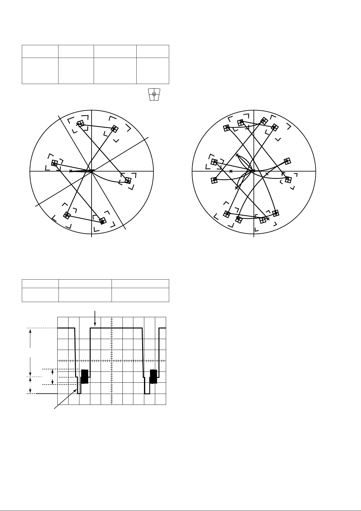
TEST MODE
PLAY + DISC SKIP test04 TIMER ON/OFF TEST MODE
FL DISPLAY:
STOP + DISC SKIP test05 VFD DISPLAY WINDOW TEST MODE
FL DISPLAY: VFD ALL LIGHT
FUNCTION: TEST THE VFD DISPLAY WINDOW
PLAY + OPEN/CLOSE test08 OPEN/CLOSE & 3 DISC CHANGER AGING TEST
CD-XP125V
DISPLAY:
FUNCTION: Enter the TEST MODE 8, MCU control the 3 DISC CHANGER OPEN/CLOSE.
After open finished, tray rotate 1 circle (360 degree). Then close, After close
finished, tray rotate 1 circle (360 degree) again.
Request: Every period include 4 operation. Below is TIMING:
Enter test mode
CHANGER
Find the disc 1 position
open
delay 3S after open finish
rotate 1 circle
close
delay 3S after close finish
rotate 1 circle
– 13 –
Page 14
CD-XP125V
PLAY + VOLUME DOWN test06 FRONT PANEL KEY TEST
FL DISPLAY:
FUNCTION:
F RONT PANEL KEY TEST MODE,IF ALL KEY HAVE BEEN PRESSED 1 TIME,
THEN
PRESS THE "POWER" KEY, VFD DISPLAY "OK".
PLAY + VOLUME UP test03 VOLUME TEST MODE
FL DISPLAY:
FUNCTION:
1. TEST 3 DISPLAY 1 SECOND. THEN CHANGE TO CD FUNCTION.
2. IN CD FUNCTION (Pickup IN CHECK DISC1 SW TOC_IL No
DISC RECEIVE OPEN/CLOSE KEY OPEN RECEIVE
OPEN/CLOSE KEY CLOSE)
3. Can change to other function [TAPE/TUNER] FUNCTION KEY PROCESS
SAME AS NORMAL PROCESS.
4. In any function within this test mode VOLUME CONTROL HAS
3LEVEL [0/23/MAX] CANCEL VOL UP/DOWN CONTINUE PROCESS
FUNCTION.
PLAY + TUNER test02 TUNER TEST MODE
FL DISPLAY
FUNCTION STORE 10 PRESET TUNER IN THE MEMORY [AM/FM ST]
FM test use the BAND key change from FM ST.
– 14 –
Page 15
NOTES ON SCHEMATIC DIAGRAM
• Resistor:
To differentiate the units of resistors, such symbol as K and
M are used: the symbol K means 1000 ohm and the symbol
M means 1000 kohm and the resistor without any symbol is
ohm-type resistor. Besides, the one with “Fusible” is a fuse
type.
• Capacitor:
To indicate the unit of capacitor, a symbol P is used: this
symbol P means pico-farad and the unit of the capacitor
without such a symbol is microfarad. As to electrolytic
capacitor, the expression “capacitance/withstand voltage”
is used.
(CH), (TH), (RH), (UJ): Temperature compensation
(ML): Mylar type
(P.P.): Polypropylene type
• Schematic diagram and Wiring Side of P.W.Board for this
model are subject to change for improvement without prior
notice.
CD-XP125V
• The indicated voltage in each section is the one measured
by Digital Multimeter between such a section and the chassis with no signal given.
1. In the tuner section,
indicates AM
indicates FM stereo
2. In the main section, a tape is being played back.
3. In the deck section, a tape is being played back.
4. In the power section, a tape is being played back.
5. In the CD section, the CD is stopped.
• Parts marked with “ 1 ” ( ) are important for
maintaining the safety of the set. Be sure to replace these
parts with specified ones for maintaining the safety and
performance of the set.
REF. NO DESCRIPTION POSITION
SW1 OPEN/CLOSE ON—OFF
SW2 DISC ON—OFF
SW3 UP ON—OFF
SW4 PICKUP IN ON—OFF
SW5 TAPE 1 PLAY ON— OFF
SW6 TAPE 1 FF/REW ON—OFF
SW7 TAPE 2 FF/REW ON—OFF
SW8 TAPE 2 PLAY ON— OFF
SW101 VOLTAGE SELECTOR 110 V—127 V—
220 V— 230-240 V
SW301 SPAN SELECTOR 50 kHz/9 kHz—
100 kHz/10 kHz
SW701 ON/STAND-BY ON—OFF
SW702 CD ON—OFF
SW703 TUNING UP ON—OFF
SW704 PRESET UP ON—OFF
TYPES OF TRANSISTOR AND LED
FRONT
VIEW
REF. NO DESCRIPTION POSITION
FRONT
VIEW
SW705 TUNER (BAND) ON—OFF
SW706
SW707 PRESET DOWN ON—OFF
SW708 EQUALIZER/X-BASS/DEMO ON—OFF
SW709 TAPE ON—OFF
SW710 STOP ON—OFF
SW711 VOLUME UP ON—OFF
SW712 DISC SKIP ON—OFF
SW713 OPEN/CLOSE ON—OFF
SW714 PLAY/REPEAT ON—OFF
SW715 VOLUME DOWN ON—OFF
SW716 P.B.C ON—OFF
SW717 O.S.D ON—OFF
SW718 DIGEST ON—OFF
SW801 REC./P.B. ON—OFF
TUNING DOWN
ON—OFF
FRONT
VIEW
E C B
(S) (G) (D)
(1) (2) (3)
2SC1740 SR
2SD1858 R2
KRA102 M
KRC102 M
KRC107 M
KRC104 M
KSA1015 GR
HSB562 C
HSC1609 GR
KSC1815 GR
KSC3203 Y
KSA1271 Y
SC1674 C
B C E
2SD2012 Y SD3210W
– 15 –
Page 16
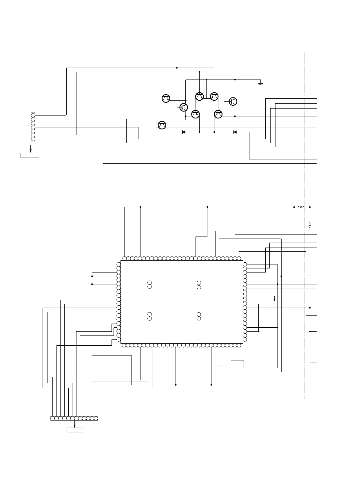
CD-XP125V
CNS933B
7
6
5
4
3
2
1
CNS933B
TO
POWER PWB
LOAD+
MECHA_UP SW
DISC1_SW
OP/CL SW
ROTATE
LOAD–
CD_STB
81
82
83
84
85
86
87
88
89
90
91
92
93
94
95
96
97
98
99
100
7980 78
XVDD
DVDD
DVR
LO
DVSL
TEST1
TEST2
TEST3
BUS0
BUS1
BUS2
BUS3
VDD
VSS
BUCK
/CCE
TEST4
TESTO
1
7776 75747372
XI
XO
VDD
XVSS
/HSO
UHSO
EMPH
LRCK
Q406
Q409
I02
VSS
I00
I01
DATA
SFSY
VSS
SBSY
Q407
VDD
50
49
32
31
SPCY
FLGD
VREF
TRO
LPFO
LPFN
SPDA
FLGC
COFS
FLGB
MONIT
Q408
Q410
D403
717069 68 676665 64 636261 60 595857 56 55545352 51
PXO
VSS
81
82
99
100
PXI
BCK
VSS
TESI01
DVSR
RO
/TSMOD
/RST
AOUT
DOUT
98765432
I03
TESIN
/DACT
/CKSE
/DMOUT
IC402
TC9462F
SERVO DSP
MBOV
IFP
SBOK
CLCK
VDD
Q405
FLGA
VDD
SEL
2VREF
TESIOO
P2VREF
Q403
DMO
HSSW
D402
FVO
FMO
FOO
TEZI
TSIN
SBAD
RFRP
RFZI
RFCT
AVDD
SLCO
AVSS
VCOF
VCOREV
PVREV
ZDET
PDO
293028272625242322212019181716151413121110
Q402
TEBC
RFGC
TEI
FEI
RFI
TMAXS
TMAX
50
49
48
47
46
45
44
43
42
41
40
39
38
37
36
35
34
33
32
31
DGND
/RST
BUS0
BUS1
BUS2
BUS3
CNP931B
PICK_IN
BUCK
/CCE
9 10111282134657
POWER PWB
LRCK
TO
BCK
DATA
CNS931B
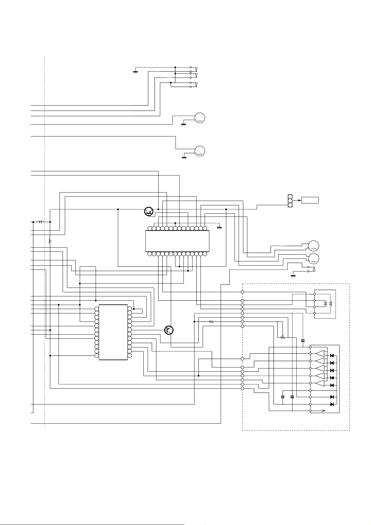
Figure 16 BLOCK DIAGRAM (1/6)
– 16 –
Page 17
OP/CL_SW
DISC1_SW
MECHA_UP SW
ROTATE+
CD-XP125V
SW1
OPEN/
CLOSE
SW2
DISC
SW3
UP
+
–
M+
M3
T/T UP/DOWN
MOTOR
M
13
14
15
16
17
18
19
20
21
22
23
24
IC401
TA2109F
SERVO PRE
AMP.
Q461
GND
OPO
IC404
PO1–
MM1469XH
FOCUS/TRACKING/
12
11
10
9
8
7
6
5
4
3
2
1
PO1+
SPIN/SLED DRIVER
VO2–
VO3–
Q401
VO2+
VO3+
19 20 21 2223 24 252627 2818171615
VIN2
VIN3
VG2
VG3
GND
VCC
MUTE
VCC
TRB
REG O
BIAS
VG4
+
–
VG1
VIN4
VIN1
VO4+
M
1234567891011121314
VO1+
VO4–
VO1–
GND
PU_IN
M1
CD LOADING
MOTOR
CD_6.2V
TR–
TR+
FO+
FO–
GND
PD
VR
LD
C
F
B
A
E
1/2V
+5V
PICKUP UNIT
+B7
CNS932
1
2
3
SP+
SP–
SL+
SL–
PU-IN
CNP932
+
–
+
–
M
M
NM802
SPINDLE MOTOR
NM801
SLED MOTOR
SW4
PICKUP IN
FO+
TR+
TR–
FO–
ACTUATOR
1/2VCC
+
–
C
+
–
F
+
–
B
+
–
A
+
–
E
GND
MON
LD
VCC
GH6C605B3A1
Figure 17 BLOCK DIAGRAM (2/6)
– 17 –
Page 18

CD-XP125V
IC10
IX0041SJ
ROM 256Kx16
VPP
VCC
PGM/A18
A17
A14
A13
A8
A9
A11
OE
A10
CE
D7
D6
D5
32
31
30
29
28
27
26
25
24
23
22
21
20
19
18
17
1
2
A16
3
A15
4
A12
5
A7
6
A6
7
A5
8
A4
9
A3
10
A2
11
A1
12
A0
13
D0
14
D1
D2D3D4
15
VSS
16
Q11
Q12
VDAC
MCLK
TSD
TBCK
TWS
7980 78 77 76757473 72717069 68 67666564 63 626160 59 58575655 54 535251
LA9
LA8
LA7
LA6
LA5
LA4
LA3
LA2
LA1
VCC
81
LA12
82
83
LA13
84
LA14
85
LA15
86
LA16
87
LA17
88
AUDIOCLK
89
AUDATA
90
BCLK
91
LR
92
93
RSD
94
RBCLK
95
RWS
96
TDMCLK
97
TDMDR
98
TDMFS
DCAS
99
VSS
100
VSS
LA11
LA10
DRAS
DWE
DA0
DA1
DA2
DA3
VCC3
1920 181716 15 141312 11 10
A2
A3
VCC
VSS
A4A5A6A7A8
DA4
A0
A1
NC
WE
RAS
OE
LA0
LSCE0
IC15
ES3880F
VIDEO CD DECODER
DA5
DA6
DA7
DA8
DBUS0
DBUS1
98765432
D4
D5
D6
D7
NC
NC
UCAS
NC
LCAS
D8D9D10
LSCE1
LROMCE
DBUS2
DBUS3
VCC
VSS
D11
LOE
DBUS4
D2
D3
D12
D13
LD7
LWR
DBUS5
DBUS6
D1
D14
3940383736353433323130292827262524232221
LD6
LD5
DBUS7
DBUS8
1
D0
VCC
VSS
D15
LD4
LD3
DBUS9
DBUS10
LD2
LD1
LD0
AUX1/DSADATA
DBUS11
DBUS12
DBUS13
VSS
AUX5
VCC3
AUX4
DSC_STB
AUX6/SCK
AUX7/STB
AUX3/VD_DI
AUX2/VD_DO
AUX0/DSAACK
PCLKQSCN
PCLK2XSCN
DCLK
HSYNC
VSYNC
YUV7DRAS1/DOE
YUV6
YUV5
YUV4
YUV3
YUV2
YUV1
YUV0
VCC3
DBUS14
DBUS15
VSS
RESET
293028272625242322212019181716151413121110987654321
50
49
VD_DI
48
VD_DO
47
46
45
44
43
42
41
40
39
38
37
36
35
34
33
32
31
IC16
IX0025SJ
D-RAM 256Kx16
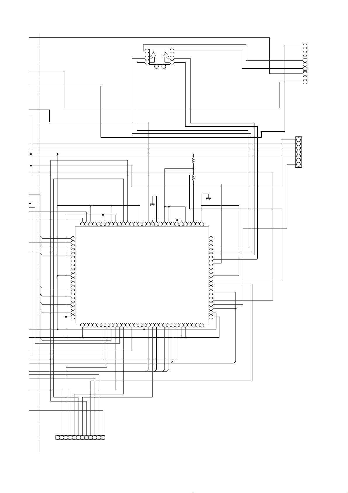
Figure 18 BLOCK DIAGRAM (3/6)
– 18 –
CNP801
1
Page 19
VDAC
IC11
NJM4565M
BUFFER AMP.
CD-XP125V
CNS802A
VDAC
1
TO
2
7
– +
6
5
1
+ –
2
3
8
4
+5V
L-CH
R-CH
+B11
+B10
+12V
VD_DI
VD_DO
3
1
2
3
3
2
1
CNP804A
1
BUSY
2
VD_DI
3
VD_DO
ACK
4
STB
5
6
CLID_OUT
7
VIDEO OUT
SECTION
CNS802B
TO
MAIN
SECTION
CNS802C
TO
POWER
SECTION
FROM DISPLAY
7980 78 77 76757473 72 717069 68 67666564 63 62616059 58 575655 54 535251
NC
XIN
VSS
VSS
81
82
83
84
85
86
87
88
89
90
91
92
93
94
95
96
97
98
99
100
PCLK2X
DSC_D7
HSYNC
DSC_D6
VSYNC
DSC_D5
YUV7
YUV6
YUV5
YUV4
VCC
VSS
YUV3
DSC_D4
YUV2
DSC_D3
YUV1
DSC_D2
YUV0
DSC_D1
VSS
1
VSS
PCLK
NC
VCC
NC
VSS
NC
VCC
DSC_CLK
VCC
XOUT
VIDEO CD ENCODER
AUX0
AUX1
DSC_STB
DSC_D0
AUX4
AUX5
ES3883F
AUX2 AUX3
RST
VCC
AUX6
IC14
NC
AUX7
ACAP
VDAC
VCC
MCLK
VSSAV
VSSAV
TWS
AUX8
201918171615141312111098765432
YDAC
VCCA
AUX9
TSD
VCCA
TBCK
CDAC
VSSAV
RSTOUT
RWS
RSET
COMP
VSSAV
BUSY/AUX15
S_EN/ AUX14
LA18/ AUX13
NC/ AUX12
NC/ AUX11
NC/ AUX10
VSS
VSS
SQCK
VREF
VREFM
MIC2
MIC1
AOL+
AOL–
AOR–
AOR+
VCCA
VREFP
VSSA
RBCK
NC
SQSO
29302827262524232221
VSSA
VCM
RSD
VCC
VSS
NC
50
49
48
47
46
45
44
43
42
41
40
39
38
37
36
35
34
33
32
31
CNP801
AUX0
EAUX0
EAUX01
EAUX02
EAUX03
EAUX08
EAUX04
910111287654321
/RST
BUS0
FROM CD SERVO SECTION
BUS2
BUS1
BUS3
/CCE
BUCK
LRCK
PICK_IN
BCK
DATA
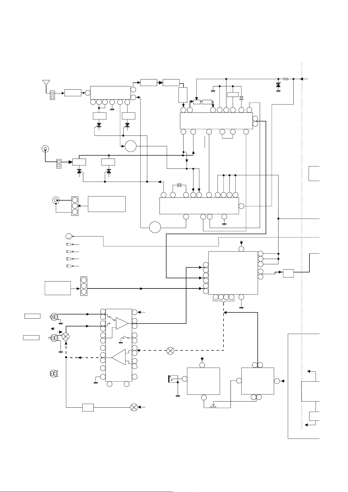
Figure 19 BLOCK DIAGRAM (4/6)
– 19 –
Page 20
CD-XP125V
V
3
0
A
A
M
T
7
SO301
FM ANTENNA
TERMINAL
AM LOOP
ANTENNA
CNP301
B.P.F
BF301
AM TRACKING
T302
TA7358AP
1
FM FRONT END
4
2
3
FM RF
L302
T306
IC301
5
COVERAGE
8
7
FM
OSC
L303
OSC BUFF
Q302
AM BAND
FM IF
T302
CF303
DZ5.1BSJ
+B4
6
9
FM OSC
VT
1
23
AM OSC IN
X352
4.5 MHz
CF302
2
AM MIX
IC303
LA1832S
21
AM RF IN
T351
AM IF
CF352
AM IF
7
STEREO
CF351
4
985
GND
VCC
FM/AM
MPXIN
OUT
18
IC303
LA1832S
FM IF DET./
FM MPX./AM IF
FM
DET
16
17
VCO
X351
456 kHz
13
MO/ST
FM/AM
12
L
14
R
15
FRO
SEC
CNS
TAPE 2
PLAYBACK
HEAD
TAPE 1
RECORD/
PLAYBACK HEAD
VIDEO OUT
T1 FF/REW
T2 FF/REW
CD SECTION
L-CH
R-CH
L-CH
R-CH
AC BIAS
ERASE
HEAD
SO103
SW5
T1 PLAY
SW6
SW7
SW8
T2 PLAY
FROM
CNS103
REC
P.B.
CNP802A
M2
TAPE
MOTOR
M
SWITCHING
SW801
B, C, D,
1
2
3
CNP103
F, G
BIAS
OSC
FROM
DECODE SECTION
CNS802A
SP DET
+B3
+B3
+B3
+B3
1
2
3
PLAYBACK AND RECORD
L(T1)
R(T1)
L(T2)
R(T2)
L NF
R NF
IC801
AN7345K
/PLAYBACK AMP.
1
24
2
23
3
22
P.B
6
L REC
REC
9
16
R REC
REF
14
Q801
L801
12
T1/T2
19
15
20
OSC
LC72131
PLL(TUNER)
7
FM
SWITCHING
+B4
13
L
4
PB
R
21
Q360
FM
TUNER
IC302
TAPE
CD
1615
FM/AM
L
R
L
R
L
R
11
9
10
15
11
14
12
13
22
1
5
20
7
18
8
17
10
SW801
H
L REC
R
L NF
R NF
ALC
+B4
SW801
A, E
JK901
MIC
5
NJM4558D
+B4
8
IC902
BUFFER
AMP.
7
MIC VOLUME
Figure 20 BLOCK DIAGRAM (5/6)
– 20 –
DO
CL
DI
CE
4
5
3
6
17
MO/ST
21
10
+B4
23
IC601
LC75341M
AUDIO PROCESSOR
VR901
8
7
3
17
18
5
1
DI
CE
2
CL
24
21
R
L
4
R
L
1 7
IC901
NJM4558D
BUFFER
AMP.
2 6
8
Q203
Q204
SYSTEM
MUTE
+B4
+B11
+B10
MC78
VOLT
REGUL
5 V
IC9
Q931
Q932
11.7
Page 21
CD-XP125V
03
04
TEM
TE
+B4
FROM CD
SECTION
CNS702
CNP702
1
2
3
4
5
6
2
1
~
3
SW701
L
R
IC201
LM1876TF
POWER AMP.
FL701
FL DISPLAY
31
10
29
15
~
26
30
~
37
CD +B
~
18
5
8
13
VccB
15
+B1
VccA
2
4
Vee
11
7
–B1
30
5251
IC701
SC16312
SYSTEM
MICROCOMPUTER
DIN
STB
VIDEO +B
CLK
68
9
11
R-OUT
L-OUT
T3.15A L 250V
F101
14
+B2
VDD
+B4
46
VDD
3332
VEE
VDD
KEY3
KEY1
~
+B2
38
13
~
10
KEY
SW702~SW715
JK101
HEADPHONES
27
-B2
CNP105
1
2
3
FROM CD
SECTION
4
CNS105
5
6
SP DET
9
SO102
SPEAKER
TERMINAL
+B11
IC931
MC7805CT
VOLTAGE
REGULATOR
Q931,
Q932
+B10
11.7 V
5 V
Q935,
Q936
VF2
VF1
+B7
+B2
+B3
+B4
+B5
-B2
5.6 V
M10 V
VOLTAGE
REGULATOR
A12 V
-30 V
6.2 V
D108~D111
IC101
MC7805CT
VOLTAGE
REGULATOR
Q103
Q104
VOLTAGE REGULATOR
Q109,Q110
VOLTAGE REGULATOR
Q935,Q936
D112~D115
VOLTAGE
REGULATOR
D934~D937
Q933,Q934
Q101
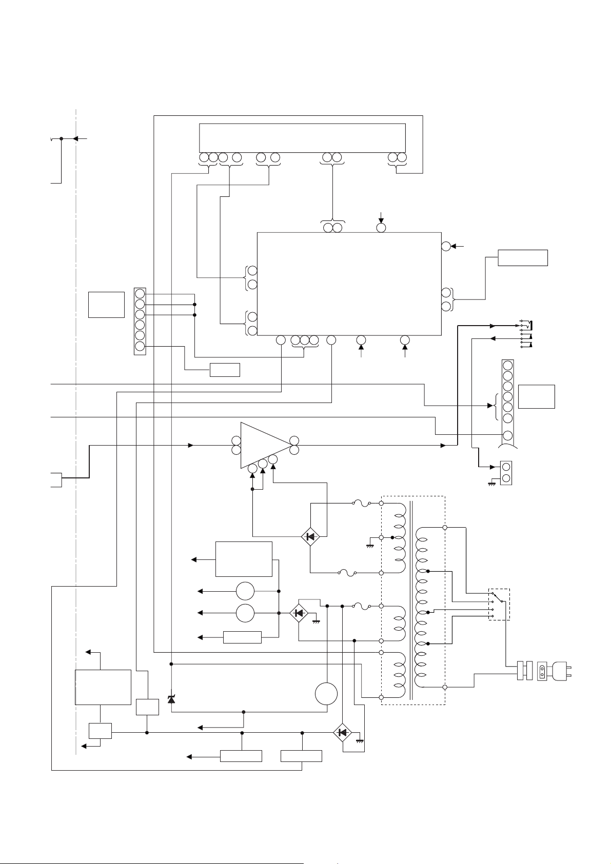
Figure 21 BLOCK DIAGRAM (6/6)
– 21 –
F102
T3.15A L 250V
F931
T2A L 250V
T101
POWER TRANSFORMER
230-240 V
220 V
127 V
110 V
SW101
VOLTAGE
SELECTOR
AC POWER
SUPPLY CORD
AC 110/127/220/
230-240 V,
SO101
AC INPUT
50/60 Hz
Page 22

CD-XP125V
B
C
MIC_MUTE
10 kHz
100 kHz/
CNS101
SPAN
4321
CL
DISPLAY PWB
6
5
DI
CE
FROM
P35 8-G
7
TAPE_DET
SELECTOR
SW301
SPAN
9 kHz
50 kHz/
CNS105
CNP105
SD
DO
A
FM ST
P_STB
D_GND
CHANEL_SW
FROM
DISPLAY PWB
P35 9-G
CNP101
123456
P_MUTE
B
SD
1
FM ST
2
DO
3
CL
4
CE
5
DI
6
+B
A_12V
7
P27 12 -A
D_GND
8
9
10
11
TUN_L
TUN_R
A_GND
C141
100/16
C
TO TUNER SECTION
C142
0.022
R129
10
A_GND
A 12V
+B
+B
CNP802B
+B
CNS802B
CD_R
A_GND
123
CD_L
FROM
DECODE PWB
P33 12-A
D
D108
1N5402M
D109
E
F
CNS104
FROM
POWER PWB
P28 2-A
1
2
3
4
5
6
7
T3.15A L250V
CNP104
F101
F102
T3.15A L250V
C101
100/50
D101
1N4004
VF1
VF2
C103
0.1
C104
0.1
C102
100/50
D102
1N4004
D111
1N5402M
C105
0.1
C106
0.1
C107
220/50
D103
1N4004
1N5402M
D110
1N5402M
D112
1N4004
D115
1N4004
ZD101
DZ300BSB
22K
R101
Q101
KSA1015 GR
C108
47/50
+B
–B
1N4004
R103
47K
R102
10
1N4004
D114
D113
G
H
• NOTES ON SCHEMATIC DIAGRAM can be found on page 15.
+B
C109
330/35
ZD102
DZ6.2BSA
–B
CNP102
+B
A_GND1
C118
Q104
R110
+B
47
3
(METAL)
4.7K
R111
C113
100/25
R113
D104
R114
2200/35
C115
0.022
22K
1N4148
22K
+B
C116
0.022
–B
+B
C112
4700/35
+B
+B
Q103
R133
820
2SD2012 Y
+B
+B
+B
820
R108
R107
100
C111
ZD103
DZ6.2BSC
1
2
Q112
KRA102 M
47
R109
(METAL)
HSC1609 GR
13V
ZD103A
DZ3.3BSB
100/25
32
KRC107 M
2SD2012 Y
Q102
1
Q111
C110
12K
100/50
R104
R105
330
R106
330
+B
+B
–30V
5.6V
3.8V
3.8V
CNS102
D_GND
4231
5
FROM
DISPLAY PWB
P34 6-G
C117
2200/35
C119
10/16
C143
R121
220/25
100
D119A
1N4004
D119
1N4004
+B
M_GND
IC101
MC7805CT
VOLTAGE
REGULATOR
3
1
2
C123
0.047
+B
C124
+
47/25
1
23456
Figure 22 SCHEMATIC DIAGRAM (1/14)
– 22 –
Page 23

CD-XP125V
WB
A
B
M_GND
IC101
C7805CT
VOLTAGE
EGULATOR
3
2
4
C123
0.047
4
CHANEL_SW
+B
–B
+B
+B
C124
47/25
M_10V
–B
+B
TAPE_DET
M_GND
A_GND
+B
P25 12-A
+10V
+B
1K
R202
TAPE SECTION
REC R
TAPE R
1K
R201
+B
10K
R207
KSC1815 GR
ZD201
DZ3.3BSB
TO
2345678910 1
REC L
TAPE L
R624
3.9K
R625
3.9K
R
L
VCC B
15 14 13 12 11 10
+B
+B
C208
470/16
R221
47K
10K
R208
Q201
10K
R216
R616
4.7K
R617
4.7K
STB B
R212
R214
10K
R211
R619
+IN B
1K
1K
+B
ZD204
DZ3.3BSB
R618
33K
33K
R220
4.7K
R620
2.7K
TAPE L
TUN L
CD L
CD R
TUN R
TAPE R
R621
2.7K
IC201
LM1876TF
POWER AMP.
–IN B
MUTE B
GND B
1K
R203
C201
47/50
Q204
KSC1815 GR
Q203
KSC1815 GR
HSC1609 GR
R215
C207
47/25
111210
L1L2L3
R1
1413
1K
VEE
ZD203
DZ3.3BSB
R608 1K
R606 1K
R3
R2
15
R607 1K
R609
OUT A
C204
47/50
+B
C205
100/16
R614
7.5K
R627
2.7K
C607
9876
R4
16
C608
1K
R615
7.5K
VCC A
C604 10/16
C605 10/16
C606 10/16
R604
1K
IC601
LC75341M
AUDIO
PROCESSOR
C601 10/16
C602 10/16
C603 10/16
+IN A
STB A
987654321
1K
R224
R213
L
R
Q202
4.7K
–IN A
1K
C203
47/50
R205
100K
R206
100K
R204
C202
47/50
R217
+B
1K
–B
10K
R605
R601 1K
R602 1K
R603 1K
MUTE A
GND A
–B
R219
10K
R218
10K
10K
R210
10K
R209
FM SIGNAL
PLAYBACK SIGNAL
RECORD SIGNAL
CD SIGNAL
MIC SIGNAL
MAIN PWB-A1(1/3)
4.7/50
L4
LSL0
RSL0
17
4.7/50
OUT B
R610
18
C610
R626
R611
C609
LIN
RIN
47K
2.2/50
2.7K
3.9K
R612
47K
C622
C611 0.0027
C613 0.1(ML)
5432
LBS
LTRE
RBS
RTRE
212019
2.2/50
C614
0.1(ML)
C612
0.0027
R613
3.9K
0.1
LOUT
ROUT
0.1
C623
CL
CE
DI
C615
VREF
C616
C617
2.2/16
VSS
2322
2.2/16
33/16
R622
100K
CE
VDD
24
C133
0.0047
1
C618
C127
C128
C125
C126
R119
R623
100K
220P
C619
220P
C620
DI
CL
R123 10
R120
4.7
0.1
0.1
0.1
0.1
4.7
100/16
L102
C621
L101
C134
0.0047
R122
10
220P
+B
CNS108
HEADPHONES PWB-A4
MIC_MUTE
L-CH
R-CH
D_GND
VCC
CNP108
L IN
L OUT
A_GND
R OUT
R IN
54321
54321
R IN
HEADPHONES
CNP107
1
2
3
4
5
+
–
–
+
1
2
3
4
5
R OUT
A_GND
JK101
L OUT
L IN
L103
10µH
CNS107
FROM
MIC PWB
P29 7-H
R-ch
L-ch
BI108
390
R128
SO102
SPEAKER
TERMINAL
390
R127
7
8 9 10 11 12
Figure 23 SCHEMATIC DIAGRAM (2/14)
– 23 –
Page 24

CD-XP125V
C822
R819
R820
R817
A
B
C
TAPE 2
PLAYBACK HEAD
R-CH
L-CH
D
MAIN PWB-A1(2/3)
SW5
TAPE 1
PLAY
SW6
TAPE 1
FF/REW
SW7
TAPE 2
FF/REW
SW8
TAPE 2
PLAY
M
+
–
M2
TAPE
MOTOR
PLAYBACK SINGAL
RECORD SINGAL
1
1
2
2
3
3
CNP801
T1_R
A_GND
T1_L
C801
560P
C802
560P
CNP803
4
4
3
3
2
2
1
1
D802
1N4148
2
3
2
1
1
CNP804
R801
1K
R802
1K
R806
27
C808
330P
D804
1N4148
R808
10K
C810
100/25
C812
0.0027
C815
0.033
R809
100K
R834
33K
+B
R835
20K
D803
1N4148
33K
R813
D806
1N4148
C819
5.6K
R815
0.0022
R818
E
TAPE 1
PLAYBACK/RECORD
HEAD
L-CH
R-CH
F
ERASE HERD
G
560P
C813
R811
C817
C805
330P
SW801C
REC./P.B.
R
CNP802
1
1
2
2
3
3
4
4
P
SW801D
REC./P.B.
R
SW801B
REC./P.B.
P
R
P
SW801F
REC./P.B.
P
SW801G
REC./P.B.
R P
T2_R2
T2_R1
A_GND
T2_L1
T2_L2
R
C803
560P
C804
560P
RECORD/PLAYBACK AMP.
R804
1K
IC801
AN7345K
PLAYBACK AND
24 23 22 21 20 19 18 17 16
R(T2)
L(T2)
C809
27
R805
10K
R NF
L NF
330P
560P
C814
R810
100K
C816
0.033
PRO
PLO
R814
33K
R(T1)
L(T1)
1 2 3 4 5 6 7 8 9
R803
1K
330P
C806
C811
100/25
R807
C807
0.0027
47/25
3.9K
L:T1
H:T2
IC801
AN7345K
3.9K
R812
C818
47/25
5.6K
R816
RRI
RLI
C821
C820
0.0022
3.3/50
R NF
L NF
RRO
RLO
H
• NOTES ON SCHEMATIC DIAGRAM can be found on page 15.
1
23456
Figure 24 SCHEMATIC DIAGRAM (3/14)
– 24 –
Page 25

CD-XP125V
C813
C814
-A1(2/3)
R834
R835
20K
D803
1N4148
8
C812
0.0027
8
R813
C815
0.033
R809
100K
33K
+B
33K
D806
1N4148
C819
5.6K
R815
0.0022
R838
5.6K
5.6K
R817
6.8K
R818
R821
C823
0.0027
1.5K
R837
1K
R824
100
R823
C827
0.022
47K
C829
0.0033
10K
R826
C831
R828
47K
47/25
+B
C840
220/16
CHANEL_SW
TAPE L
TAPE R
REC R
REC L
+10V
M_GND
A_GND
TAPE_DET
M_10V
1
2
3
4
5
6
7
8
9
10
P23 7 - A
TO MAIN SECTION
C825
3.3/50
R NF
L NF
22/50
RRO
RLO
ALC
10 11 12
C822
0.022
6.8K
R819
5.6K
R820
REF
C826
22/50
C824
0.0027
560P
R811
C817
47/25
3.9K
L:T1
IC801
AN7345K
3.9K
R812
C818
5.6K
R816
33K
H:T2
47/25
RRI
RLI
C821
C820
0.0022
21 20 19 18 17 16 15 14 13
PRO
PLO
4 5 6 7 8 9
560P
R810
100K
C816
0.033
R814
+B
VCC
R822
R
P
1.5K
SW801E
REC./P.B.
SW801A
REC./P.B.
C828
0.022
100
R825
P
R
C830
0.0033
C833
22/50
C834
C832
10K
R827
220/16
+B
47/25
C835
0.022
R836
8.2K
C836
0.0022
(ML)
R829
220
+B
D805
1N4148
L801
BIAS OSC.
C837
100/10
SW801H
REC./P.B.
R830
220
C838
0.022 (ML)
+B
D801
1N4004
P R
+B
R831
150
R832
33K
C839
0.0047
(ML)
BIAS OSC.
KSC1815 GR
R833
Q801
10
7
8 9 10 11 12
Figure 25 SCHEMATIC DIAGRAM (4/14)
– 25 –
Page 26

CD-XP125V
B
3
4
A
MAIN PWB-A1(3/3)
B
C
D
E
AM LOOP
ANTENNA
SO301
FM ANTENNA
TERMINAL
FM SIGNAL
AM SIGNAL
C302
0.001
D301
1N4148
D302
1N4148
BF301
B.P.F
123
123 4 56 7 8 9
C319
18P(CH)
D306
1N4148
C320
1N4148
C304
0.01
0.001
C305
0.0047
D305
D307
1N4148
CNP301
AM
1
1
GND
2
2
FM
C301
0.012
0.8V
C306
C307
9P(UJ)
0.0047
1.5V
FM RF
C308
L302
0.022
5.2V
C318
C303
0.001
C309
5P
R302
R301
22
0.001
100K
1.5V
33K
R303
VD303
KDV147B
AM TRACKING fL
AM ANTENNA
C329
0.022
C337
0.022
FM FRONT END
0V
5.2V
FM IF
C311
10P(CH)
R304
47K
R315
33
OSC BUFF
T302
AM OSC.
T306
AM BAND
COVERAGE fL
IC301
TA7358AP
47
R307
T304
FM OSC.
FM BAND
COVERAGE fL
Q302
SSC1674 C
C335
560P
4.4V
C312
R305
680
C315
100P
R323
68K
R306
33
33P
L303
C330
12P(CH)
3.8V
2
6P
C313
C314
22P(CH)
C316
C331
0.047
C334
27P(UJ)
CF303
13
(UJ)
R308
10K
10/16
VD302
+B
C317
0.022
C332
0.022
5.2V
+B
KDV147B
R313
680
VD301
SVC348S
R316
330
R312
2.2K
R314
33
5.6K
R336
Q306
SSC1674 C
+B
+
R
C349
0.001
F
G
H
• NOTES ON SCHEMATIC DIAGRAM can be found on page 15.
1
23456
Figure 26 SCHEMATIC DIAGRAM (5/14)
– 26 –
R310
4.7K
C321
0.0033
Page 27

CD-XP125V
TO
MAIN PWB
P22 1 - C
9
10
TUN_L
TUN_R
C374
R357
1K
R356
1/50
2.1V
100/16
121314151617
IF IN
470K
MPX IN
10
0V0V5V
C355
47K
R395
5.6K
R377
C386
0V
IF REQ
56P
C369
1.3V
R-CH
IF OUT
11
3.8V
(1.9V)
C356
0.001
22P
330P
R365
0.022
1.3V
OUT
L-CH
PHASE
C357
2.2/50
1/50
C370
C383
R387
10K
C371
1/50
OUT
0.022
5.6K
C373
0.022
C372
1/50
C358
R361
4.7K
R362
4.7K
1/50
13141516
MO/ST
PHASE
12
R376
3.3K
R364
4.7V
(0V)
4V
(AM/FM)
3.8V
(1.2V)
3.3K
R355
+B
10K
L352
100µH
100/16
+B
(2.2V)
C396
R391
390
IC303
+B
1
3.3K
R363
Q351
32
R366
2.2K
LA1832S
FM IF DET./
FM MPX./AM IF
C395
0.022
+B
R392
390
11.7V
R383
5.6K
R384
5.6K
R385
6.8K
D308
1N4148
KRC104 M
ZD351
DZ5.1BSB
10.8V
10.9V
Q360
KSA1015 GR
C391
47/25
+B
+B
SWITCHING
FM MUTE
LEVEL
R358
VR351
8.2K
10K(B)
+B
L353
1mH
5.6K
R351
5.6K
R336
2.1V
C351
0.022
16
0
2
14
Q306
SSC1674 C
+B
R309
470
+B
+B
1
CF302
+B
3
2
C384
0.001
C343
2.1V
33P
C344
C382
15P(CH)
33P
C360
0.022
C362
3.3/50
5V
24
2.5V
IN
OUT
AM OSC
AM OSC
REG
AM MIX
OUT
IN
FM IF
123
5V
C352
10/16
C378
330P
+B
C397
0.022
330
R382
330
R386
22 21 20
12P
2.6V
(CH)
C381
X352
4.5 MHz
12 3456 7 89
2.6V
IC302
LC72131
PLL(TUNER)
+B
C361
0.022
2.1V
(2.7V)
2223
FM AFC
LA1832S
C350
0.022
VT
R381
VSS
X OUT
0V
X IN
AM IF
10K
(2.7V)
2.1V
IN
AM RF
IC303
T351
C394
C393
AOUT
R374
C364
10/16
C365
0.022
C363
0.022
(0.9V)
0V
0.6V
2021
VSM
AM IF
IN
456 78
1K
R352
1
3
2
CF352
47/25
C392
0.001
1.5K
R380
1/50
19
0.9V
AIN
CE
DICLDO
4.8V
0.1V
0.1V
1K
1K
1K
R373
R371
R372
1819
CUT
FM/AM
AM LOW
GND
C353
0.022
C380
10/16
2.2K
R379
18
0.9V
PD
5.1V
1K
2.3V
OUT
SD
C366
5V
+B
1.7V
0.001
R350
C367
C354
C387
0.022
5.2V
FM
(11.4V)
2.7K
1/50
STEREO
5V
0.022
(0V)
2.6V
VDD
FM IN
MUTE
3.7V
X351
FM DET
CF351
100µH
0V
AM IN
FM
(0V)
3.9V
456 kHz
17
2.3V
MPX VCO
2.9V
(4.3V)
270
R353
C399
+B
R393
1K
L351
0.01
C385
(2.6V)
10 11
3.5V
C368
(0V)
VCC
9
C398
0.022
MO/ST
R359
(0V)
1.8K
R360
4.7K
21
SD
FM ST
11
A_GND
3
DO
7
4
CL
8
6
5
DI
CE
A_12V
D_GND
+B
+B
7
8 9 10 11 12
Figure 27 SCHEMATIC DIAGRAM (6/14)
– 27 –
Page 28

CD-XP125V
A
CNS104
BI104
TO
MAIN PWB
P22 1-E
CNP104
F931
T2A L 250V
132
173562
7
8
64 54
B
T101
POWER
TRANSFORMER
SO101
50/60 Hz
AC INPUT
AC 110/127/220/230-240 V,
110 V
127 V
220 V
SW101
VOLTAGE
SELECTOR
230-240 V
1N4004
D937
1N4004
D936
C935
C934
0.1
0.1
D935
1N4004
D934
1N4004
C
3
1
Q938
KRC107 M
2
3
R940
820
1
Q937
C936
2
KRA102 M
AC POWER
SUPPLY CORD
D
E
F
10/25
R939
100
ZD931
DZ130BSA
R932
4.7K
C937
47/25
C941
0.047
C940
47/25
C939
100/25
Q932
20V
HSC1609 GR
13V
Q931
20V
R931
2SD2012Y
12.3V
47
D938
1N4148
R933
22K
C938
0.022
D939
D940
1N4004
1N4004
1
2
3
IC931
MC7805CT
ZD932
DZ8.2BSC
C943
220/25
R935
100
R934
4.7K
C944
100/25
1
3
2
VOLTAGE REGULATOR
C942
4700/35
3
KRC107 M
2
1
Q934
KRA102 M
Q936
HSC1609 GR
D942
1N4148
C945
0.022
C946
470/16
Q933
R938
22K
R941
R936
820
2.7K
R937
47
1N4004
D941
+B2
Q935
2SD2012 Y
CD_6.2V
POWER PWB-A2
FROM
CD SERVO PWB
G
CNP931B
1
CNP931A
1
FC801
H
30 2-H
CNS931B
CNP801
8243657
10
982436571
TO
DECODE PWB
P33 7-H
12910
11
12
11
12
• NOTES ON SCHEMATIC DIAGRAM can be found on page 15.
1
23456
Figure 28 SCHEMATIC DIAGRAM (7/14)
CNP802C
FROM
DECODE PWB
P33 12-B
– 28 –
5V
123
CNS802C
D_GND
11.7V
VIDEO+B
1
FROM
DISPLAY PWB
P35 8-A
CD+B
CNP932
CD SERVO PWB
1
CD_STB
LOAD–
ROTATE
CNS933A
FROM
P30 1-C
CNS933B
OP/CL_SW
D_GND
M_GND
MECHA_UP_SW
DISC1_SW
CD_6.2V
312
756234
LOAD+
98243657
CNP933B
CNP933A
CNS932
FROM
CD SERVO PWB
P31 11-D
Page 29

MIC SIGNAL
C903
100/16
IC902
NJM4558D
BUFFER
AMP.
CD-XP125V
JK901
MIC
R901
2.7K
C901
0.0015
C902
0.22/16
R917
10K
R903
39K
R904
330
1
2
3
4
C906
4.7/16
R906
1K
8
7
6
5
C905
470P
C907
100/16
C904
220P
R905
33K
+B
+B
1K
R902
10K
R919
R918
TO_CPU
1.6K
C911
C913
1/16
R914
12K
470P
R908
10K
VR901
R910
5.6K
5.6K
R912
4
3
2
1
IC901
NJM4558D
BUFFER
AMP.
R909
5.6K
R907
10K
R916
39K
470P
C910
5
6
7
8
R911
C912
1/16
R913
12K
5.6K
+B
MIC_MUTE
9V
D_GND
R-CH
L-CH
54321
6
CNP107
TO
MAIN PWB
P23 11 - B
7
432 1
5
8 9 10 11 12
BI107
CNS107
MIC PWB-A3
Figure 29 SCHEMATIC DIAGRAM (8/14)
– 29 –
Page 30

CD-XP125V
6
K
A
B
C
D
E
F
CNS933B
7
6
5
4
3
2
1
CNS933B
TO
POWER PWB
P28 4-G
CD SERVO PWB-B2
BI933B
LOAD+
7
MECHA_UP SW
6
DISC1_SW
5
OP/CL SW
4
ROTATE
3
LOAD–
2
CD_STB
1
C440
100/16
R449
220
C468 220P
C467 220P
C466 220P
R455 100K
R453 100K
R454 100K
R452 100K
C464
220P
R444 1K
R443 1K
R442 1K
R447 1K
R446 1K
R445 1K
R441 1K
C436
C430
0.056
C462
0.001
100/16
C428
100/16
C469
220P
C435
0.056
C437
470P
0V
2.4V
0V
C465
220P
5V
5V
5V
4.9V
C425
0.056
5V
5V
81
82
83
84
85
86
87
88
89
90
92
93
94
95
96
97
98
99
100
FB401
F0010SJ
C426
15P(CH)
1K
R420
2.2V
2.6V
7980 78
XO
XVDD
DVDD
2.3V
DVR
2.4V
LO
0V
DVSL
TEST1
TEST2
TEST3
4.3V
BUS0
4.3V
BUS1
4.3V
BUS2
4.3V
BUS3
5V
VDD
0V
VSS
4V
BUCK
3.3V
/CCE
TEST4
TESTO
/HSO
1
5V5V5V
Q409
KSC1815 GR
FB402
F0010SJ
C427
15P(CH)
C424
0.056
X402
0V0V5V
5V
7776 757473 72
XI
PXI
PXO
VDD
XVSS
81
82
99
100
UHSO
EMPH
LRCK
VSS
BCK
0V
0V
1.4V
2.5V
22K
R430
22K
3.3K
1.5K
R437
R434
Q408
R438
KSC3203 Y
6.8K
Q410
KSA1271 Y
D403 1N4004
C431
0.022
L406
0V
0V0V0V0V0V
5V
I03
/DACT
/CKSE
/DMOUT
IC402
TC9462F
SERVO DSP
IFP
SBOK
CLCK
VDD
0V0V0V
5V
5V
1.2V
C420
0.01
10µH
I02
VSS
0V0V0V
I01
DATA
5V
I00
SFSY
2.4V
C470
0.022
717069 686766 656463 626160 5958 57 5655 54 5352 51
VSS
TESIN
TESI01
DVSR
RO
/TSMOD
/RST
AOUT
DOUT
MBOV
98765432
0V0V0V
2.5V
Q406
KSC1815 GR
3.3K
R431
KSA1271 Y
C423
0.01
C422
220/6.3
0V
0V
5V
VSS
VDD
FLGD
50
49
32
31
SBSY
SPCY
SPDA
0V
0.6V
Q407
0V
FLGC
VREF
TRO
LPFO
LPFN
COFS
1.7V
C429
5V
FLGB
MONIT
0V
100/10
R415
0V
5V
2.5V
FLGA
VDD
0V
Q405
R419
4.3V
SEL
2VREF
TESIOO
P2VREF
4.3V
1.5K
R418
KSC1815 GR
3.3K
Q403
KSA1271 Y
D402 1N4004
R414 3.3K
R412 3.3K
2.2K
R411
0V
2.1V
2.2V
2.1V
FVO
FMO
DMO
TEBC
FOO
TEZI
TSIN
SBAD
RFRP
RFZI
RFCT
AVDD
RFI
SLCO
AVSS
VCOF
VCOREV
PVREV
HSSW
ZDET
PDO
TMAXS
293028272625242322212019181716151413121110
0V
2.1V
2.1V
2.1V
R401
10K
C438
47/10
Q402
KSC3203 Y
C419
0.1
C418
0.1
R410
3.3K
1.8V
50
49
RFGC
48
47
TEI
46
45
44
FEI
43
42
41
40
39
38
37
36
35
34
33
32
31
TMAX
R404
100K
R402
2.1V
47K
2.1V
2.1V
2.2V
2.2V
2.2V
2.1V
2.1V
2.2V
2.1V
2.1V
2.1V
5V
2.1V
2.1V
0V
1.4V
2.1V
2.1V
2.1V
2.1V
C417
R406
15K
0.1
R409
10K
R408
3.3K
C407
0.033
0.0027
C401
100P
C405
C404
0.01
C403
47/10
C421
C402
0.015
0.1
C409
0.0047
R407
10K
C406
0.0047
C410
0.001
C411
47/25
L403
10µH
C412
0.01
L401
C413
10µH
100/10
C450
100/16
C448
39P
R429
220/6.3
C445
68K
C449
0.056
R428
1.2K
R427
39K
R42
2.7
PICK_IN
BUS2
BUS3
BUCK
/CCE
9 10111282134657
9 10111282134657
LRCK
BCK
DATA
BI931B
CNS931B
TO
POWER PWB
P28 2-G
DGND
/RST
BUS0
BUS1
G
CNP931B
H
• NOTES ON SCHEMATIC DIAGRAM can be found on page 15.
1
23456
Figure 30 SCHEMATIC DIAGRAM (9/14)
– 30 –
Page 31

CD-XP125V
SWITCH B PWB-B4
+
–
M3
T/T UP/DOWN
MOTOR
+
–
M1
CD LOADING
MOTOR
C4A
SW1
OPEN/
CLOSE
SW2
DISC
SW3
UP
M
M
FO+
TR+
TR–
FO–
ACTUATOR
1/2VCC
+
–
C
+
–
F
+
–
B
+
–
A
+
–
E
GND
MON
LD
VCC
GH6C605B3A1
1
2
3
4
BI401
M+
M–
CNP402
BI932
BI405
SP+
SP–
SL+
SL–
PU-IN
GND
TR–
TR+
FO+
FO–
GND
PD
VR
LD
BI406
BI407
VREF
+5V
CNS401
1
1
2
2
3
4
1
2
3
4
1
2
3
3
4
CNS932
1
2
3
1
2
3
4
CNS402
CNP932
TO
POWER PWB
P28 5-G
T/T UP/DOWN
MOTOR PWB-B6
1
2
BI402A
CD LOADING
MOTOR PWB-B5
1
2
CD MOTOR PWB-C
+
CNS405
7
6
5
4
3
2
1
1
2
3
4
5
6
7
8
9
CNS406
CNS407
C
1
2
F
3
B
4
A
5
E
6
7
8
SP–
5
SL+
6
5
4
3
2
1
1
1
2
2
3
3
4
4
5
5
6
6
7
7
8
8
1
1
2
2
3
3
4
4
5
5
6
6
7
7
4
3
2
1
TR–
TR+
FO+
FO–
GND
PD
VR
LD
C
F
B
A
E
1/2V
+5V
SL–
PU-IN
GND
CNP405
+
–
SP+
6
M
–
M
NM802
SPINDLE MOTOR
NM801
SLED MOTOR
SW4
PICKUP IN
VR1A
C3A
C2A
M_GND
OP/CL_SW
DISC1_SW
MECHA_UP SW
ROTATE+
ROTATE–
C461
C459 470/10
C460 0.1
68K
0.0022
C487
0.0027
R439 1K
Q461
HSB562 C
6.3V
5V
3
H
GND
L401
C413
10µH
100/10
C450
100/16
C448
39P
R429
220/6.3
C445
68K
C449
0.056
R428
1.2K
R427
39K
R426
2.7K
C444
0.0068
C446
0.1
C439
2P
R425
82K
C447
0.1
IC404
R423 1K
2.1V
13
14
2.2V
15
2.1V
16
2.1V
17
2.1V
18
2.1V
19
2.1V
20
2.1V
21
2.1V
22
1.7V
23
0V 2.1V
2.1V
24
C455
100/16
MM1469XH
C458 0.01
FOCUS/TRACKING/
SPIN/SLED DRIVER
12
2.2V
11
2.1V
10
4.3V
9
2.1V
8
2.5V
7
3.4V
6
0V
5
2.1V
4
2.1V
3
2.1V
2
5V
1
IC401
TA2109F
SERVO PRE
AMP.
OPO
PO1–
C457 47/25
R424
47K
PO1+
C441
3.4V
VO2–
VO3–
100/16
4.1V
VO2+
VO3+
19 202122232425 26272818171615
VIN2
VIN3
2.2K
R462
VG2
GND
VG3
VCC
C442
47/25
R422
KSA1015 GR
2V
MUTE
VCC
33
Q401
TRB
REG O
BIAS
VG4
R463
2.2K
C443
0.1
VG1
VIN4
R461
VIN1
VO4+
2.2K
R40F
82K
VO1+
VO4–
R421
150
1234567891011121314
VO1–
R40B
68K
GND
R40E
82K
R40A
82K
R40C
82K
R40G
PU_IN
M_GND
D_GND
CD_6.2V
PICKUP UNIT
7
8 9 10 11 12
Figure 31 SCHEMATIC DIAGRAM (10/14)
– 31 –
Page 32

CD-XP125V
BUS1
EAUX01
C
L
A
B
C122A
0.1
C
IC10
IX0041SJ
ROM 256Kx16
+B
VPP
1
2
A16
PGM/A18
3
A15
4
A12
5
A7
6
A6
7
A5
8
A4
9
A3
10
A2
11
A1
12
A0
13
D0
14
D1
D2D3D4
15
VSS
16
VCC
A17
A14
A13
A11
A10
A8
A9
OE
CE
D7
D6
D5
C125A
100/10
32
31
30
29
28
27
26
25
24
23
22
21
20
19
18
17
+B
R123A
75
C103A
22/25
+B
R124A
220
R113A
100
Q12
2SC1740 SR
C101A
1000/6.3
R112A
56
R92
4.7K
VDAC
R111A
2.2K
+B
C131
+B
R167A
33
Q11
2SD1858 R2
+B
R143A
0.1
C105A
220
4.7K
0.1
C112A
0.1
C126A
R5
+B
22/25
C115A
VIDEO SIGNAL
CD SIGNAL
+B
R98
4.7K
R91 4.7K
C104A
100/10
R97
4.7K
R121A
3.3K
R114A
6.8K
R93
4.7K
22/25
C121A
R12A
4.7K
R163A
33
R164A
10
+B
R165A
10
R09A
4.7K
R08A
4.7K
0.1
C127A
C183A
22P(CH)
0.1
C108A
4.7K
+B
4.7K
R162A
22/25
C102A
MCLK
TSD
TBCK
TWS
0.1
C110A
C109A
4.7K
R170A
R161A 33
R166A 33
R168A 33
R169A
33
R157A 1.5K
R158A 1.5K
R159A 1.5K
4.7K
R160A
+B
R156A
D
E
F
G
7980 78 777675 747372 71 706968 676665 64636261 605958 575655 54 535251
100/10
81
82
83
84
85
86
87
88
89
90
91
92
93
94
95
96
97
98
99
100
VCC
LA12
LA13
LA14
LA15
LA16
LA17
AUDIOCLK
AUDATA
BCLK
LR
RSD
RBCLK
RWS
TDMCLK
TDMDR
TDMFS
DCAS
VSS
0.1
C111A
LA9
LA8
VSS
VCC3
+B
LA7
LA11
LA10
DRAS
DWE
DA0
DA1
DA2
1920 18 171615 141312 11 10
A0A1A2
A3
VCC
VSS
NC
A4A5A6A7A8
LA6
LA5
LA4
LA3
LA2
LA1
LA0
LSCE0
LSCE1
IC15
ES3880F
VIDEO CD DECODER
DA3
DA4
DA5
DA6
DA7
DA8
DBUS0
DBUS1
DBUS2
98765432
D4D5D6
D7
NC
NC
WE
RAS
D8D9D10
UCAS
OE
LCAS
IC16
IX0025SJ
D11
NC
VSS
LOE
LROMCE
DBUS3
DBUS4
0.1
C116A
D3
VCC
D12
LD7
LWR
DBUS5
DBUS6
D13
D14
D0D1D2
D15
3940383736353433323130292827262524232221
LD6
DBUS7
D-RAM 256Kx16
LD5
DBUS8
+B
1
VCC
VSS
LD4
LD3
LD2
LD1
DBUS9
DBUS10
DBUS11
DBUS12
C117A 0.1
C118A 22/25
LD0
VSS
AUX5
VCC3
AUX4
DSC_STB
AUX6/SCK
AUX7/STB
AUX3/VD_DI
AUX2/VD_DO
AUX1/DSADATA
AUX0/DSAACK
PCLKQSCN
PCLK2XSCN
DCLK
HSYNC
VSYNC
YUV7DRAS1/DOE
YUV6
YUV5
YUV4
YUV3
YUV2
YUV1
YUV0
VCC3
DBUS13
DBUS14
DBUS15
VSS
RESET
293028272625242322212019181716151413121110987654321
0.1
C119A
50
49
VD_DI
48
VD_DO
47
46
45
44
43
42
41
40
39
38
37
36
35
34
33
32
31
0.1
C120A
H
• NOTES ON SCHEMATIC DIAGRAM can be found on page 15.
1
23456
Figure 32 SCHEMATIC DIAGRAM (11/14)
– 32 –
AUX0
EAUX0
321
/RST
BUS0
DGND
1
Page 33

CD-XP125V
111A
2.2K
08A
.7K
R167A
33
VDAC
C131A 0.001(CH)
+B
C183A
0.1
C127A
L11
22P(CH)
81
82
83
84
85
86
87
88
89
90
91
92
93
94
95
96
97
98
99
100
+B
C130A
0.1
C143A
33P(CH)
C141A
33P(CH)
R185A
R181A
R187A 10K
R189A 10K
10/25
C139A
R178A
82
+B
C124A
0.1
VCC
AUX6
AUX4
AUX5
IC14
ES3883F
NC
RST
AUX7
33
R142A
R02A
4.7K
R03A
4.7K
7
6
5
10K
100K
R183A
10/25
ACAP
VCC
0.1
C135A
– +
C149A
100K
VDAC
MCLK
8
0.1
C148A
VSSAV
AUX8
R10A
4.7K
R107A
10K
IC11
NJM4565M
BUFFER AMP.
+B
27P
C129A
TC100
PCLK
NC
VCC
NC
VSS
NC
NC
VSS
VCC
DSC_CLK
H1004SJ
C184A
0.1
7980 78 777675 747372 71 706968 676665 64 636261 605958 57 565554 535251
PCLK2X
DSC_D7
HSYNC
DSC_D6
VSYNC
DSC_D5
YUV7
YUV6
YUV5
YUV4
VCC
VSS
YUV3
DSC_D4
YUV2
DSC_D3
YUV1
DSC_D2
YUV0
DSC_D1
VSS
VSS
1
R01A
4.7K
C137A
R171A
100K
X1
27 MHz
XIN
VSS
VCC
XOUT
VIDEO CD ENCODER
AUX0
AUX1
AUX2 AUX3
DSC_STB
DSC_D0
C106A 1
4
100/10
6.8K
R103A
R195A
YDAC
VSSAV
AUX9
TWS
201918171615141312111098765432
+ –
100
R11A
C147A
100/10
R104A
VCCA
VCCA
TBCK
TSD
4.7K
33P(CH)
1
2
3
10K
R184A
+B
C136A
0.1
CDAC
RWS
+B
C144A
R186A
R182A
100K
R194A
270
VSSAV
RSTOUT
10K
C140A
R193A
4.7K
C171A
10/25
R108A
10K
C142A
33P(CH)
100K
R188A 10K
10/25
L103A
3.3µH
RSET
COMP
VSSAV
BUSY/AUX15
S_EN/ AUX14
LA18/ AUX13
NC/ AUX12
NC/ AUX11
NC/ AUX10
VSS
VSS
SQCK
C172A
10/25
R190A 10K
10/25
C138A
L104A
3.3µH
+B
VREF
VSSA
VREFM
MIC2
MIC1
AOL+
AOL–
AOR–
AOR+
VCCA
VREFP
VCM
VSSA
RBCK
RSD
VCC
VSS
NC
NC
SQSO
29302827262524232221
+B
+B
4.7K
R06A
100K
R101A
+B
C150A
0.1
50
49
48
47
46
45
44
43
42
41
40
39
38
37
36
35
34
33
32
31
C164A
47/10
4.7K
R07A
+B
R116A
15K
R102A
C158A
C159A
R105A
R115A
15K
100K
100/10
C165A
R100A
0.1
4.7K
C167A
0.1
C169A
C162A
0.1
4.7K
22P(CH)
VD_DI
VD_DO
C160A
0.1
C166A
0.1
22/25
22P
C168A
C161A
+B
100/10
R94A 4.7K
+B
+B
R137A 1K
R138A 33
R139A 1K
R140A 1K
R141A 1K
NTSC
PAL
BI802
VDAC
AGNDV
L-CH
AGNDA
R-CH
+5V
DGND
+12V
CNS802A
1
3
4
5
6
7
8
9
CNP804A
1
BUSY
2
VD_DI
3
VD_DO
ACK
4
STB
5
DGND
6
CLID_OUT
7
1
22
3
1
2
3
3
2
1
CNS802B
CNS802C
TO
VIDEO OUT PWB
P35 12-E
CNS802A
CNS802B
CNS802C
TO
POWER PWB
P28 4-G
CNS804
FROM
DISPLAY PWB
P35 12-E
TO
MAIN PWB
P22 5-A
AUX0
EAUX0
EAUX01
EAUX02
EAUX03
EAUX08
EAUX04
87654321
/RST
BUS3
BUS2
BUS1
BUS0
DGND
1
BUCK
CNP931
7
9101112
/CCE
LRCK
PICK_IN
POWER PWB
P28 2-H
CNP801A
BCK
DATA
12
FC801
TO
8 9 10 11 12
DECODE PWB-D
Figure 33 SCHEMATIC DIAGRAM (12/14)
– 33 –
Page 34

CD-XP125V
A
1
B
C
8
A
DISPLAY PWB-B1
B
VF1
G8
C
D
E
SW708
EQUALIZER
X-BASS/DEMO
SW702
CD
SW703
TUNING UP
SW704
PRESET
UP
VFD701
G5G6G4
G1
G3
G2
987654321
G7
FL DISPLAY
P3P2P4
P1
SW705
TUNER
(BAND)
SW706
TUNING
DOWN
SW707
PRESET
DOWN
P9
P5
P10
P6
P7
P8
P11
P12
P13
–30V
SW709
TAPE
SW710
STOP
SW711
VOLUME
UP
VF2
P14
333231302928272625242322212019181716151413121110
SEG9
23
SEG10
24
SEG11
25
SEG12/GRID11
26
VEE
27
SEG13/GRID10
28
SEG14/GRID9
29
SEG15/GRID8
30
SEG16/GRID7
31
GRID6
32
GRID5
33
-B
34 35 36 37 38 39 40 41 42 43 44
SW712
DISC SKIP
SW713
OPEN/CLOSE
SW714
PLAY/
REPEAT
SW715
VOLUME
DOWN
D702 1SS133
D703 1SS133
D701 1SS133
D705 1SS133
SEG7
SEG8
SEG6/KS6
SEG5/KS5
SEG4/KS4
IC701
PT6312
SYSTEM
MICROCOMPUTER
LED3
LED4
VDD
GRID1
GRID2
GRID3
GRID4
C711
5V
0.047
SW716
P.B.C
SW717
O.S.D
SW718
DIGEST
D704 1SS133
5V
VDD
SEG3/KS3
SEG2/KS2
SEG1/KS1
OSC
GND
LED1
LED2
R711
56K
KEY4
KEY2
KEY1
GND
DOUT
SW4
SW3
SW2
SW1
1213141516171819202122
STB
CLK
DIN
KEY3
C712
100P
R704
10K
11
10
R703
C713
100P
9
8
7
6
5
4
3
2
1
10K
RX701
N64H380A
321
C701
100/10
R702
47
D_GND
R705
10K
R706
10K
C704
100P
C705
100P
R710
10K
R709
10K
R707
10K
-B
+B
R735
270
KSC1815 GR
+B
+B
+B
C702
0.047
Q704
C703
100P
LED701
SD3210W
+B
R70
R70
(MET
1K
R
2
18
F
G
H
• NOTES ON SCHEMATIC DIAGRAM can be found on page 15.
1
23456
Figure 34 SCHEMATIC DIAGRAM (13/14)
– 34 –
BI102
CNS102
3.8V
MAIN PWB
–30V
3.8V
3456
3451122
CNP102
TO
P22 3-H
GND
5V
Page 35

CD-XP125V
–30V
X701
4H380A
21
2
47
C703
100P
LED701
SD3210W
04
15 GR
+B
CNS933A
BI933A
R701
1K
INTR
R742
2.7K
R708
18
(METAL)
+B
TIMER_LED
DATA
CLK
R765
1K
C706
100/16
STB
CD+B
Video+B
C707
0.033
CNP933B
421897635
421897635
LOAD–
CD_STB
R756
1K
ROTATE
DISC1_SW
OP/CL_SW
R750 1K
TO
POWER PWB
P28 4-H
LOAD+
MECHA_UP SW
R736 1K
R738 1K
R740 1K
R743 1K
R745 1K
R747 1K
R748 1K
R753 1K
R751 1K
R754 1K
R752 1K
R712 10K
R713 10K
R714 10K
LOAD–
37
38
39
40
41
42
43
44
45
DI
46
DO
47
CL
48
R755 1K
R757 1K
1K
R730
R729 1K
R728 1K
R727 1K
LOAD+
STB
CLK
DATA
OP/CL_SW
MECHA_UP SW
DISC1_SW
ROTATE
CD_STB
IX0055SJ
NRST
MMOD
SD
DI
FM_ST
P_MUTE
P_STB
CE
1
R758
1K
R764
R731
VCD_STB
P0W_KEY
IC702
CD+B
R761
1K
1K
R763
R720
10K
1K
1K
R732
252627282930313233343536
IR
24
23
VCD_CLK
22
VCD_IN
SYS_STOP
TAPE-CHK
8765432
1K
21
DEMO-KEY
TIMER-LED
TAPE-SEL
SPAN-SW
9
VCD_OUT
20
19
XO
18
XI
17
VSS
16
OSC1
OSC2
15
VDD
14
R749
13
1.8K
Vedio+B
12
11
10
C709
100/10
MIC_MUTE
IX0055SJ
1K
SYSTEM
R759
MICROCOMPUTER
+B
R737
1K
VCD_BUSY
IC702
D711
1N4148
CLID1
X701
8 MHz
R723
1K
C708
0.1
R739 1K
R741 1K
R744 1K
R746 1K
C710
0.1
R721
D708
1N4004
+B
1K
VDD
+B
L702
2.2µH
R718
3.3K
Q702
KRC102 M
D709
1N4148
C730
3.3/16
C731
0.01
R724
100K
D710
1N4148
VIDEO OUT
PWB-B7
D_GND
P0W_KEY
CNP701
R716 1K
KSC1815 GR
SO103
VIDEO OUT
Q701
R726
82
CNS701
3
2
1
R719
10K
KSC1815 GR
SWITCH A PWB-B3
SW701
ON/
STAND-BY
3
2
2
1
1
BI701
R717
10K
R722
ZD701
120
DZ3.3BSB
Q703
3
2
1
VCD_STB
VCD_CLK
VCD_OUT
VCD_BUSY
CNP802A
DECODE PWB
CLID1
GND
VCD_IN
BI804
CNS802A
FROME
P33 12-A
R725
1K
7
6
5
4
3
2
1
CNS804
7
6
5
4
3
2
1
DECODE PWB
P33 12-C
CNP804
TO
5V
456
345
02
WB
-H
GND
SDDODICLCE
FM_ST
7
5367124
5367124
CNP105
TO
MAIN PWB
P22 2-A
TAPE_CHK
BI105
CNS105
P_MUTE
P_STB
TAPE_SEL
CNP101
TO
MAIN PWB
P22 3-A
SPAN_SW
GND
231546
231546
MIC_MUTE
BI101
CNS101
8 9 10 11 12
Figure 35 SCHEMATIC DIAGRAM (14/14)
– 35 –
Page 36

CD-XP125V
1
5
P
4
S
R
A
A
MAIN PWB-A1
P40
DISPL
CN
F
B
75 OHMS
ANTENNA
C
D
E
F
G
SO301
FM ANTENNA
TERMINAL
FM
GND
AM LOOP
SW302
SPAN
SELECTOR
100 kHz/10 kHz
50 kHz/9 kHz
SO102
SPEAKER
TERMINAL
L-CH
R-CH
JK101
2
1
HEADPHONES
2
1
CNP301
C302
C349
C301
L101
R127
TP301
BF301
L102
R128
R380
R304
Q302
23
L103
B
C
E
C304
D305
D307
D301
R381
C397
C315
R305
C319
R123
C380
C394
C321
R315
R122
C129
C133
22
R379
15
C393
C316
R119
R120
C134
BI108
IC302
20
R365
C387
9
8
7
C317
6
5
C311
4
3
C320
2
C318
11
C306
L302
1
5
1
R374
C381
C392
C382
5
10
1112
C383
R309
R316
IC301
C312
C314
R306
R301
T304
C305
C307
D306
C303
VD301
T302
C126
C127
F101
T3.15A L 250V
F102
T3.15A L 250V
CNS108
BK
GY
GY
GY
GY
R373
R372
R371
R359
R360
C329
1
2
3
4
5
L303
C308
C309
C330
C384
R387
L351
VD302
R308
R303
R307
R302
C331
C128
R310
C313
CF303
VD303
C332
C335
C334
R323
C125
POWER PWB
X352
C386
C385
L353
VR351
LEVEL
FM MUTE
R336
3
R312
2
1
T306
C103
C104
1
23 4567
CNS104
FROM
P42 6-E
CF302
123
R314
C337
D308
C378
T351
B
R313
C
E
Q306
C362
D108
D109
CNP104
C343
R386
R382
1
2
3
R352
1 5 10 12
24
R358
CF352
C351
20
C365
C364
Q360
C398
CF351
C352
R353
IC303
C366
R350
E
C
B
C370
C344
C367
C399
R351
C350
C369
R383
C355
TP302
CNP108
54321
D110
C360
C361
1315
R356
R357
L352
C356
C368
D111
R391
R392
R385
R384
C374
R395
R376
C354
C372
R364
Q104
C353
R362
B
C
E
R109
B
C
Q103
E
ZD351
C357
R355
C358
C363
X351
C371
C373
E
C
B
C391
R377
R393
R363
R361
R110
Q102
D104
R111
C395
C396
C124
ZD103
C142
C123
R114
C119
C113
R366
C116
C115
C141
3
2
1
R113
ZD103A
Q351
R129
C143
3
2
1
13
Q111
3
R121
R107
R108
D119A
123
C106
C105
C112
IC101
212
R133
D119
CN
D
D1
D1
D11
Q112
C111
D106
HEADPHONES PWB-A4
P44 5 - D
FROM
TAPE MOTOR
H
1
23456
Figure 36 WIRING SIDE OF P.W.BOARD (1/9)
– 36 –
Page 37

CD-XP125V
Q
Q351
41
R129
3
2
1
C143
13
111
3
R107
R108
DISPLAY PWB
1234567
C106
C105
C112
IC101
3
2
1
212
R133
R121
D119A
P40 3-G
FROM
CNS105
CNP105
D112
D115
Q112
C111
D106
D119
D113
D114
DISPLAYO PWB
C101
D101
D102
C102
R106
R105
C204
13579111315
C203
2468101214
IC201
P40 4-G
FROM
CNS101
654321
CNP101
C107
D103
C110
R104
ZD102
12345
CNP102
R210
ZD203
C118
C117
C202
R205
R203
R204
R206
R224
R101
R209
Q203
B
C
E
R213
Q101
ZD101
C108
ECB
R218
R219
C201
P41 11 - C
FROM
DISPLAY PWB
CNS102
E
C
R103
B
C109
ZD201
R207
R208
R217
Q202
C205
R220
CNP804
R825
R822
R827
R202
R201
C820
C818
C814
C816
R214
R212
Q204
ECB
R102
C207
CNP803
C828
C826
C832
R810
C811
R216
D802
3
2
1
R814
R807
4
3
2
1
R215
B
C
E
R211
ZD204
D805
C806
R801
D803
R838
C822
C821
R816
R812
C801
P43 7-G
FROM
DECODE PWB
CNS802B
R618
C618
C208
R601
R221
Q201
3
2
1
CNP802B
1
2
3
4
CNP107
5
C837
D804
R834
R833
R837
R836
R835
D806
R829
C833
C830
C835
C834
12 13
10
5
IC801
1
C805
C809
R802
R806
3
C802
2
R804
1
R803
C804
CNP801
C617
R623
C615
R610
C836
C840
15
20
24
C803
CNP802
C616
C623
R613
C612
C620
C619
R602
R603
L801
Q801
ECB
C829
C831
C819
R813
C817
C813
C815
R809
SW801
REC./P.B.
C810
C808
4
3
2
1
R625
R611
R622
R626
C614
C610
R605
R607
R609
IC601
C621
1 5 1012
C611
R612
C622
C609
C613
R614
R624
C838
R831
C839
R832
R830
D801
R826
R818
R815
R811
A
R808
C812
B
C
C807
DH
R805
R627
C823
R820
C824
G
R621
C608
152024
C825
E
F
REC.
R615
13
R608
R606
R604
C607
R828
C827
P.B.
C606
R620
R617
R821
R819
R619
C601
R616
R824
R817
C602
C603
C604
C605
R823
MIC PWB-A3
VR901
MIC VOLUME
R902
C902
C904
IC902
R912
C911
C913
BI107
1
R914
CNS107
P44 5 - A
FROM
TAPE MECHANISM
S103
VIDEO OUT
3
2
1
CNP802A
JK901
MIC
C901
R903
R901
R904
8765
C905
R906
R905
1234
R908
R907
R910
R909
R916
4
5
3
6
7
2
IC901
8
1
6
R913
WHGYGYGYGY
12345
COLOR TABLE
BR
RD(R)
OR
YL
GR
BL
VL
GY
WH(W)
BK
PK
C903
C907
C906
R917
R919
R911
C910
C912
BROWN
RED
ORANGE
YELLOW
GREEN
BLUE
VIOLET
GRAY
WHITE
BLACK
PINK
R918
P44 5 - D
FROM
TAPE MOTOR
VIDEO OUT
P44 3 - H
FROM TAPE 1
PLAYBACK/RECORD
P44 4 - H
FROM TAPE 2
PLAYBACK HEAD
7
8 9 10 11 12
HEAD
CNS802B
FROM
DECODE PWB
P43 7-G
Figure 37 WIRING SIDE OF P.W.BOARD (2/9)
– 37 –
PWB-B7
Page 38

CD-XP125V
A
CD SERVO PWB-2
B
TO
POWER PWB
C
POWER PWB
42 2-G
CNP932
CNS932
D
1
CNS401
BK
1
GY
2
GY
3
E
GY
4
F
P42 3-H
CNP933B
TO
CNS933B
123 1234567 123456789
BK
BK
GYGYGYGYGYGYGYGYGYGYGYGYGYGYGYGYGYGYGY
3
BI932
CNP402
4
3
2
1
1
BI933B
1
R437
R430
R418
BK
R415
Q410
7
GYGYGY
BI401
POWER PWB
BL
1
4
R434
ECB
P42 4-H
CNP931B
BI931B
R443
R444
C468
C469
B
C
Q408
E
TO
R447
C467
Q405
B
C
E
CNS931B
R446
C466
10 1211
R455
Q406
E
C
B
R454
R431
R419
D402
D403
R438
R453
Q402
12
R452
BCE
BCE
B
C
E
CNS405
Q407
Q403
BI405
B
C
E
7
C458
C457
R449
C465
C464
C437
R445
R441
R442
Q409
GY
C461
C436
C445
C455
GY
R439
C440
C435
100
1
Q461
FB402
C462
C430
C428
C429
R401
C401
R426
R428
R427
GYGYGY
B
C
E
5
R404
C444
C403
C446
C447
C439
123456
WH
95
C420
C438
C448
1
R461
14 15
R462
C470
C426
C487
C425
R420
81
85
75
90
10
15
20
30
C402
R406
R402
R425
13
24
1
5
7
8
10
FB401
C427
80
70
65
IC402
25
35
31
C413
C405
C418
15 10
20
25
20
L406
C424
X402
C423
60
55
45
40
C404
C417
IC401
5
IC404
28
22
21
C431
C412
R407
C406
R410
R423
R411
C442
12
1
C450
C449
R429
C443
L403
C422
R408
50 51
C407
R424
R463
C410
C409
R421
R409
R40G
R40B
R40C
R40A
R40E
R40F
C459
R414
C460
R412
E
C
Q401
B
C419
C441
BI407
1
1
BI406
9
C421
R422
C411
8
L401
GY
GY
GY
GY
GY
GY
BK
BK
GY
GY
GY
GY
GY
GY
GY
CNS406
1
2
3
4
5
6
7
8
CNS407
7
6
5
4
3
2
1
G
H
1
23456
Figure 38 WIRING SIDE OF P.W.BOARD (3/9)
– 38 –
Page 39

PICKUP UNIT(308)
17
1
8
NM802
SPINDLE MOTOR
CD MOTOR
PWB-C
6
CNP405
SW4
PICKUP IN
12345
F3895AF
B
1
NM801
SLED MOTOR
CD-XP125V
COLOR TABLE
BROWN
BR
RD(R)
OR
YL
GR
BL
VL
GY
WH(W)
BK
PK
RED
ORANGE
YELLOW
GREEN
BLUE
VIOLET
GRAY
WHITE
BLACK
PINK
SWITCH B PWB-B4
SW3
UP
1234
SW2
DISC
SW1
OPEN/CLOSE
CNS402
T/T UP/DOWN
MOTOR PWB-B6
M3
T/T UP/DOWN MOTOR
BI402A
12
BK
4
RD
3
BL
2
WH
1
CD LOADING
MOTOR PWB-B5
M1
CD LOADING MOTOR
BI402B
12
7
8 9 10 11 12
Figure 39 WIRING SIDE OF P.W.BOARD (4/9)
– 39 –
Page 40

CD-XP125V
0
D
A
B
C
D
E
F
DISPLAY -B1
C703
Q701
BCE
CE
C730
R718
R712
R713
R714
R722
R716
D711
R727
9
Q703
D710
Q702
C708
R740
R726
R725
C731
R724
R723
R743
BI933A
R720
R748
R738
B
R719
R717
ZD701
123
R721
SW713
OPEN/
CLOSE
SW712
DISC SKIP
RX701
C705
R706
SW708
EQUALIZER/
X-BASS/DEMO
R732
R736
R745
R747
R750
1
7
1
2
3
C704
R705
R756
R754
R751
BI105
R701
C701
D709
36
37
R752
R702
35
40
48
R753
30
45
C702
R709
R742
R728
R704
C713
SW711
VOLUME UP
2425
IC702
20
13
15
10
12
5
1
R765
R755
R757
R764
1
R730
R710
R729
12 34
R749
R761
R763
R758
SW715
VOLUME
DOWN
R711
D708
L702
X701
R759
C711
56789
C710
C709
BI101
6
IC701
34
33
VFD701
10 11 12 13 14 15 16 17 18 19 20 21 22 23 24 25 26 27
D704
R739
1
44
1
R746
1
35
30
40
5
15
10
11 12
SW709
TAPE
SW704
PRESET UP
SW703
TUNING UP
R741
R744
BI804
25
20
R731
R737
23
22
D705
D703
SW707
PREST
DOWN
7
SW7
TUNE
(BAN
SW706
TUNING
DOWN
WHWHWHWHWHWHWHWHBK
CNS933A
G
CNP933A
TO
POWER PWB
P42 2-H
WHWHWHWHWHWHBK
1
23456789
CNP105
TO
MAIN PWB
P37 7-A
12345612345612345677
CNS105
CNS101
WHWHWHWHWH
CNP101
TO
MAIN PWB
P37 8-A
BK
WHWHWHWHWHWHBK
CNP804A
TO
DECODER PWB
P43 10-E
CNS804
H
1
23456
Figure 40 WIRING SIDE OF P.W.BOARD (5/9)
– 40 –
Page 41

R735
CD-XP125V
324252627282930313233
SW705
TUNER
(BAND)
D702
7
T
SW706
TUNING
DOWN
R707
34
SW702
CD
D701
SW714
PLAY/REPEAT
SW716
P.B.C
SW717
O.S.D
SW718
DIGEST
E
C
Q704
B
C707
LED701
C706
R703
C712
R708
SW710
STOP
1
BI102
6
1
2
3
CNP701
BK
GY
GY
GY
GY
CNS701
CNS102
1
2
3
4
5
WH
1
BK
2
3
TO
MAIN PWB
P37 8-A
CN102
SWITCH A PWB-B3
SW701
ON/STAND-BY
BI701
1
2
COLOR TABLE
BR
RD(R)
OR
YL
GR
BL
VL
GY
WH(W)
BK
PK
7
8 9 10 11 12
Figure 41 WIRING SIDE OF P.W.BOARD (6/9)
– 41 –
BROWN
RED
ORANGE
YELLOW
GREEN
BLUE
VIOLET
GRAY
WHITE
BLACK
PINK
Page 42

CD-XP125V
AC POWER
SUPPLY CORD
A
SO101
AC INPUT
AC 110/127/220/230-240 V,
220 V
Q936
C943
R935
D934
D935
C934
C935
110 V
ECB
Q932
123
123
127 V
50/60 Hz
POWER TRANSFORMER
110 V
127 V
BI104
1
GY
GY
GY
F931
T2A L 250V
D936
D937
E
CB
R931
R936
R933
3
1
CNP802C
2
2
1
3
Q938
Q937
CNP931A
1012
CNP931B
101112
T101
CNS104
BK
7
GY
GY
GY
8
BK
GY
GY
GY
R937
Q935
E
C
B
GY
GY
GY
COLOR TABLE
BR
RD(R)
OR
R939
C937
C936
R932
ZD931
D938
Q931
E
C
B
YL
GR
BL
VL
GY
WH(W)
C939
123
2468
357911
456789
3
2
C940
IC931
D939
1
D940
C938
C941
1
1
23
BK
PK
12
FC801
1
6
MAIN PWB
5
4
3
2
1
BROWN
RED
ORANGE
YELLOW
GREEN
BLUE
VIOLET
GRAY
WHITE
BLACK
PINK
CNS802C
FROM
DECODE PWB
P43 7-G
CNP801
TO
DECODE PWB
43 7-F
TO
P36 4-G
CNP104
POWER PWB-A2
B
C
SW101
VOLTAGE SELECTOR
230-240 V
220 V
230-240 V
D
R934
ZD932
D942
E
R938
C946
C945
C944
R941
R940
D941
F
C942
FROM
CD SERVO PWB
P38 2-C
CNS932
G
FROM
DISPLAY PWB
P40 2-G
CNS933A
Q934
Q933
CNP932
CNP933A
12345678
CNP933B
1
234567
123
9
H
1
23456
CNS933B
FROM
CD SERVO PWB
P38-2-C
CNS931B
FROM
CD SERVO PWB
P38 3-C
Figure 42 WIRING SIDE OF P.W.BOARD (7/9)
– 42 –
Page 43

DECODE PWB-D (TOP AIEW)
CD-XP125V
R09A
R08A
R12A
C122A
R101A
R115A
C167A
C168A
R116A
C166A
L103A
R102A
R100A
R94A
C164A
C165A
C160A
C169A
L104A
C159A
R105A
C162A
R190A
R188A
R184A
R103A
R195A
R187A
C137A
31
C158A
50
R11A
30
51
R185A
R186A
R10A
35
40
45
C150A
C141A
C142A
R183A
R182A
R07A
C139A
R06A
25
C161A
R181A
IC11
58
R189A
C140A
C135A
R193A
20
IC14
6055
R194A
C136A
R178A
R108A
C106A
C124A
14
R142A
7065
R107A
C138A
R03A
R02A
1015 5
X1
C144A
C172A
C143A
C171A
C149A
75
C184A
R171A
C147A
C130A
C129A
C131A
R112A
R111A
R01A
95
90
85
1
80
R104A
100
81
TC100
C104A
C148A
C127A
C183A
R121A
C120A
R165A
R164A
R163A
L11
R114A
C118A
C117A
R167A
R124A
40
15
C121A
31
50
C119A
C103A
Q12
EC
C101A
30
35
40
45
51
R123A
B
R113A
25
3035
IC16
10 15
20
IC15
6055
C116A
R141A
7065
R140A
1015 5
R139A
75
R138A
95
90
85
2125
20
1
80
R137A
100
81
C108A
R92
R97
C111A
C110A
R158A
R159A
R170A
R157A
C109A
R93
C102A
R162A
R161A
R91
R156A
R160A
R169A
R168A
R166A
C115A
10
11
12
13
14
15
16
C125A
EC
R98
1
2
3
4
5
6
7
8
9
C105A
Q11
C126A
B
C112A
IC10
32
31
30
29
28
27
26
25
24
23
22
21
20
19
18
17
R143A
R5
TO MAIN
PWB-A1
CNP931A
P42 6-G
TO
VIDEO OUT PWB
P37 11-H
CNP802A
TO
MAIN PWB
P37 9-A
CNP802B
TO
POWER PWB
P42 6-G
CNP802C
FC801
CNS802A
1
2
CNS802B
1
2
3
CNS802C
1
2
3
DECODE PWB-D (BOTTOM AIEW)
1
12
RD
WH
YL
BK
BK
BL
GY
GY
CNP801A
1
2
3
4
5
6
7
8
9
10
11
12
1
CHASSIS
GND
BI802
9
CNS804
7654321
CNP804A
FROM
DISPLAY PWB
P40 5-G
7
8 9 10 11 12
Figure 43 WIRING SIDE OF P.W.BOARD (8/9)
– 43 –
Page 44

CD-XP125V
A
B
YL
RD
RD
RD
YL
OR
RD
BR
4
3
2
1
P37 11-F
CNP803
TO MAIN PWB
SW5
TAPE 1
PLAY
SW6
TAPE 1
FF/REW
SW7
TAPE 2
FF/REW
SW8
TAPE 2
PLAY
C
M2
TAPE
MOTOR
A
B
+
-
WH
BK
3
2
1
P37 7-H
CNP804
TO MAIN PWB
D
TAPE 1 TAPE 2
E
ERASE
HERAD
RECORD/PLAYBACK
HEAD
PLAYBACK
HEAD
WH
COLOR TABLE
BROWN
BR
RD(R)
OR
YL
GR
BL
VL
GY
WH(W)
BK
PK
RED
ORANGE
YELLOW
GREEN
BLUE
VIOLET
GRAY
WHITE
BLACK
PINK
RD
BK
WH
CNP802
P37 10-H
BK
4321
BK
BK
WH
RD
BK
BR
WH
BK
RD
23
1
CNP801
P37 9-H
TO MAIN PWB
F
RD
G
H
TO MAIN PWB
1
23456
Figure 44 WIRING SIDE OF P.W.BOARD (9/9)
– 44 –
Page 45

VOLTAGE
CD-XP125V
IC101
PIN
VOLTAGE
NO.
1 18 V
0.6 V
2
3
4.9 V
IC201
PIN
VOLTAGE
NO.
1 0.14 V
22 V
2
3
0.15 V
–22 V
4
0 V
5
0.3 V
6
0 V
7
0 V
8
0 V
9
10 0 V
11 0.3 V
12 0 V
13 0 V
14 0 V
15 22 V
Q407
PIN
VOLTAGE
NO.
E6 V
3 V
C
B
5.5 V
Q204
PIN
VOLTAGE
NO.
E0 V
0 V
C
B
0.6 V
Q351
PIN
VOLTAGE
NO.
E0 V
4.7 V (0 V)
C
B
3.7 V (0 V)
IC404
PIN
VOLTAGE
NO.
1 2.7 V
2.7 V
2
3
2.7 V
2.7 V
4
5.2 V
5
5.2 V
6
4.7 V
7
0 V
8
2.7 V
9
10 2.7 V
11 2.4 V
12 2.9 V
13 0 V
14 2.9 V
15 0 V
16 5.6 V
17 2.7 V
18 2.7 V
19 2.7 V
20 2.7 V
21 6 V
22 6 V
23 2.7 V
24 2.7 V
25 2.7 V
3 V
26
27
2.5 V
0 V
28
2.7 V
29
2.9 V
30
2.4 V
31
0 V
32
Q401
PIN
VOLTAGE
NO.
E5 V
2.1 V
C
B
4.2 V
Q402
PIN
VOLTAGE
NO.
E0 V
0.3 V
C
B
0 V
IC601
PIN
VOLTAGE
NO.
1 4.8 V
0 V
2
3
0 V
4.8 V
4
4.8 V
5
4.8 V
6
4.8 V
7
4.8 V
8
4.8 V
9
10 4.8 V
11 4.8 V
12 4.8 V
13 4.8 V
14 4.8 V
15 4.8 V
16 4.8 V
17 4.8 V
18 4.8 V
19 4.8 V
20 4.8 V
21 4.8 V
22 4.8 V
23 9.4 V
24 4.8 V
Q408
PIN
VOLTAGE
NO.
E0 V
0.3 V
C
B
0 V
Q403
PIN
VOLTAGE
NO.
E 5.7 V
0 V
C
B
5.3 V
IC801
PIN
VOLTAGE
NO.
10 V
1.5 V
2
3
1.5 V
1.8 V
4
0.8 V
5
0 V
6
0 V
7
0.6 V
8
3 V
9
10 3 V
11 0 V
12 0 V
13 6.2 V
14 3.8 V
15 0 V
16 3 V
17 0.6 V
18 0 V
19 0 V
20 1 V
21 1.8 V
22 0.6 V
23 0 V
24 0 V
Q405
PIN
VOLTAGE
NO.
E0 V
5.3 V
C
B
0 V
Q406
PIN
VOLTAGE
NO.
E0 V
5.3 V
C
B
0 V
Q101
PIN
VOLTAGE
NO.
E –27 V
–28 V
C
B
–23 V
Q102
PIN
VOLTAGE
NO.
E 12 V
18 V
C
B
12.5 V
Q103
PIN
VOLTAGE
NO.
E 11.4 V
18.6 V
C
B
12 V
Q104
PIN
VOLTAGE
NO.
E 11.3 V
18.5 V
C
B
12 V
Q105
PIN
VOLTAGE
NO.
E 7.9 V
18.5 V
C
B
9.3 V
Q106
PIN
VOLTAGE
NO.
E 6.8 V
18.5 V
C
B
7.9 V
Q111
PIN
VOLTAGE
NO.
E0 V
0 V
C
B
4.3 V
Q112
PIN
VOLTAGE
NO.
E 9.4 V
9.4 V
C
B
0 V
Q201
PIN
VOLTAGE
NO.
E0 V
0 V
C
B
0.7 V
Q202
PIN
VOLTAGE
NO.
E0 V
0 V
C
B
0.7 V
Q203
PIN
VOLTAGE
NO.
E0 V
0 V
C
B
0.6 V
– 45 –
Page 46

CD-XP125V
FUNCTION TABLE OF IC
IC401 VHiTA2109F/-1:Servo Pre Amp. (TA2109F)
Pin No. Input/Output Function
Terminal Name
1 VCC Input Power voltage terminal
2 FNI Input Main beam amp input terminal
3 FPI Input Main beam amp input terminal
4 TPI Input Sub-beam amp input terminal
5 TNI Input Sub-beam amp input terminal
6 MDI Input Monitor photodiode amp input terminal
7 LDO Output Laser diode amp output terminal
8 SEL Input Laser diode control signal input and APC circuit ON/OFF signal input terminal
9 TEB Input Tracking error balance adjustment signal input terminal
To be controlled by 3 -value PWM signal. (PWM carrier = 88.2 kHz)
10 2VRO Output Standard voltage (2 VR) output terminal. When Vcc = 5 V, 2 VR = 4.2 V.
11 TEN Input Tracking error signal generation amp reversed phase input terminal
12 TEO Output Tracking error signal generation amp output terminal
13 SBAD Output Sub-beam addition signal output terminal
14 FEO Output Focus error signal generation amp output terminal
15 FEN Input Focus error signal generation amp reversed phase input terminal
16 VRO Output Standard voltage (VR) output terminal. When Vcc = 5 V, VR = 2.1 V.
17 RFRP Output Track count signal generation amp output terminal
18 RFIS Input RFRP detection circuit input terminal
19 RFGO Output RF signal output terminal
20 RFGC Input RF amplitude adjustment control signal input terminal
The amplitude of RF signal can be controlled by using the 3 -value PWM signal (PWM
carrier = 88.2 kHz) which is output from the RFGC terminal of TC9432F.
21 AGCI Input RF signal amplitude adjustment amp input terminal
22 RFO Output RF signal generation amp output terminal
23 GND — GND terminal
24 RFN Input RF reversed phase input terminal
SBAD
FEO
FEN
VRO
RFRP
RFIS
RFGC
AGCI
RFO
GND
RFN
15kΩ
15kΩ
20µA
50kΩ
14
10pF
10kΩ
21kΩ 21kΩ
20kΩ
20kΩ
7.96kΩ
50µA
15
16
17
18
19
10kΩ
36pF
12kΩ
12kΩ
20kΩ
PEAK
BOTTOM
10kΩ
10kΩ
20
23.5kΩ
21
re = 130Ω
22
23
12kΩ
180kΩ
40pF
1.53kΩ
24
3.3kΩ
3.3kΩ
30kΩ
30kΩ
21kΩ 29kΩ
24kΩ
1.74kΩ
65µA
180kΩ
20pF
180kΩ
20pF
40pF
180kΩ
24kΩ
60kΩ
60kΩ
47kΩ
SW
13kΩ
3
10kΩ
SW
7.67kΩ
3 STATE
DET.
SW
1
2
680kΩ
I . I
I . I
20kΩ
20kΩ
1kΩ
2.12kΩ
LDC
20pF
20kΩ
20kΩ
1213
11
10
9
8
7
6
5
4
3
2
1
TEO
TEN
2VRO
TEB
SEL
LDO
MDI
TNI
TPI
FPI
FNI
VCC
SEL
L
HiZ
H
SW1
ON
OFF
OFF
LDC
SW2
SW3
OFF OFF
ONONON
ON
Figure 46 BLOCK DIAGRAM OF IC
– 46 –
Page 47

IC402 VHiTC9462F/-1: Servo DSP (TC9462F) (1/3)
CD-XP125V
Pin No.
1* TEST0 Input Test mode terminal. To be opened usually.
2* /HSO Output Playback speed mode flag output terminal.
3* /UHSO Output
4* EMPH Output Sub-code Q data emphasis flag output terminal. "H": Emphasis ON "L": Emphasis OFF
5 LRCK Output Channel clock (44.1 kHz) output terminal. "L": L channel "H": R channel
6 VSS — Digital ground terminal.
7 BCK Output Bit clock (1.4122 MHz) output terminal.
8 AOUT Output Audio data output terminal.
9* DOUT Output Digital out output terminal.
10* MBOV Output Buffer memory over signal output terminal. "H": Over
11* IPF Output Correction flag output terminal.
12* SBOK Output Sub-code Q data CRCC judgment result output terminal. "H": When judgment result is OK.
13* CLCK Input/Output Sub-code P-W data read clock output/input terminal. Selectable with command bit.
14 VDD Input Digital + power terminal.
15 VSS — Digital ground terminal.
16* DATA Output Sub-code P-W data output terminal.
17* SFSY Output Playback system frame sync signal output terminal.
18* SBSY Output Sub-code block sync output terminal. "H": On S1 position when the sub-code sync is detected.
19* SPCK Output Processor status signal read clock (176.4 kHz) output terminal.
20* SPDA Output Processor status signal output terminal.
21* COFS Output Correction system frame clock (7.35 kHz) output terminal.
22* MONIT Output LSI internal signal monitor terminal.
23 VDD Input Digital + power terminal.
24 TESIO0 Input Test input/output terminal. To be fixed to "L" usually.
25 P2VREF — 2VREF terminal for PLL system.
26* HSSW Output VREF voltage in case of x2 speed/x4 speed.
27* ZDET Output 1-bit DAC zero detection flag output terminal.
28 PDO Output Terminal to output the phase difference between EFM signal and PLCK signal.
29* TMAXS Output TMAX detection result output terminal. To be selected with command bit TMPS.
30 TMAX Output TMAX detection result output terminal. To be selected with command bit TMPS.
Port Name
Input/Output
/UHSO
H H x1 speed playback
H L x2 speed playback
L H x4 speed playback
LL—
The output polarity can be inverted by command.
The output polarity can be inverted by command.
"H": When AOUT output is correction-disabled symbol in case of C2 correction output.
It is possible to monitor the DSP internal flag and PLL system clock with the microcomputer
command. Terminal for serial output of text data according to command.
Terminal to input the text data read clock according to command.
/HSO
TMAX detection result
Longer than specific period "P2VREF"
Shorter than specific period "VSS"
Within specific period "HIZ"
31 LPFN Input Low-pass filter amp inverted input terminal.
32 LPFO Output Low-pass filter amp output terminal.
33 PVREF Input VREF terminal for PLL system.
34 VCOREF Input VCO center frequency standard level terminal. To be fixed to PVref usually.
35 VCOF Output VCO filter terminal.
36 AVSS — Analog system ground terminal.
37 SLCO Output Data slice level generation DAC output terminal.
38 RFI Input RF signal input terminal.
Function
Playback speed
TMAX output
In this unit, the terminal with asterisk mark (*) is (open) terminal which is not connected to the outside.
– 47 –
Page 48

CD-XP125V
IC402 VHiTC9462F/-1: Servo DSP (TC9462F) (2/3)
Pin No.
39 AVDD Input Analog system power terminal.
40 RFCT Input RFRP signal center level input terminal.
41 RFZI Input RFRP zero cross input terminal.
42 RFIP Input RF ripple signal input terminal.
43 FEI Input Focus error signal input terminal.
44 SBAD Input Sub-beam addition signal input terminal.
45 TSIN Input Test input terminal. To be fixed to Vref usually.
46 TEI Input Tacking error input terminal. (Tracking servo ON: Taking-in).
47 TEZI Input Tracking error, zero cross input terminal.
48 FOO Output Focus equalizer output terminal.
49 TRO Output Tracking equalizer output terminal.
50 VREF Input Analog standard power terminal.
51 RFGC Output RF amplitude adjustment control signal output terminal.
52 TEBC Output Tracking balance control signal output terminal.
53 FMO Output Feed equalizer output terminal. 3 -value PWM signal is output. (PWM carrier = 88.2 kHz)
54* FVO Output Speed error signal or feed search EQ output terminal.
55 DMO Output Disc equalizer output terminal.
56 2VREF Input Analog standard power terminal (2xVREF)
57 SEL Output APC circuit ON/OFF signal output terminal.
58* FLGA Output Internal signal monitor external flag output terminal.
59* FLGB Output Internal signal monitor external flag output terminal.
60* FLGC Output Internal signal monitor external flag output terminal.
61* FLGD Output Internal signal monitor external flag output terminal.
62 VDD Input Digital + power terminal.
63 VSS — Digital ground terminal.
64* IO0 Input/Output General-use I/O port.
65* IO1 The input port and output port can be selected with command. In case of input port the terminal
66* IO2 state (H/L) can be read with the read command.
67* IO3 In case of output port the terminal state (H/L/HiZ) can be controlled with command.
68* /DMOUT Input Terminal to set the mode to output 2 -value PWM of feed equalizer from IO0,1 terminal and 2 -
69* /CKSE Input To be opened usually.
70* /DACT Input DAC test mode terminal. To be opened usually.
71 TESIN Input Test input terminal (externally provided VCO clock input terminal). To be fixed to "L" usually.
72 TESIO1 Input Test input/output terminal. To be fixed to "L" usually.
73 VSS — Digital ground terminal.
74 PXI Input DSP system clock oscillation circuit input terminal. To be fixed to "L" usually.
75* PXO Output DSP system clock oscillation circuit output terminal.
76 VDD Input Digital + power terminal.
77 XVSS — System clock oscillation circuit ground terminal.
78 XI Input System clock oscillation input terminal.
79 XO Output System clock oscillation circuit output terminal.
80 XVDD Input System clock oscillation circuit + power terminal.
81 DVSR Input R channel D/A converting section power terminal.
82* RO Output R channel data forward rotation output terminal.
Port Name
Input/Output
3 -value PWM signal is output. (PWM carrier = 88.2 kHz)
3 -value PWM signal is output. (PWM carrier = 88.2 kHz)
3 -value PWM signal is output. (PWM carrier = 88.2 kHz)
3 -value PWM signal is output. (PWM carrier = DSP system 88.2 kHz, sync with PXO)
When laser is ON and UHS = L, "Hi-Z". When UHS = H, "H" output is obtained.
TEZC, FOON, FOK and RFZC signals can be selected with command.
DFCT, FOON, FMON and RFZC signals can be selected with command.
TRON, TRSR, FOK, and SRCH signals can be selected with command.
TRON, DMON, HYS and SHC signals can be selected with command.
value PWM of disc equalizer from IO 2,3 terminal. "L" active
Function
In this unit, the terminal with asterisk mark (*) is (open) terminal which is not connected to the outside.
– 48 –
Page 49

IC402 VHiTC9462F/-1: Servo DSP (TC9462F) (3/3)
CD-XP125V
Pin No.
Port Name
Input/Output
Function
83 DVDD Input D/A converting section power terminal.
84 DVR Input Reference voltage terminal.
85* LO Output L channel data forward rotation output terminal.
86 DVSL Input L channel D/A converting section power terminal.
87* TEST1 Input Test mode terminal. To be opened usually.
88* TEST2 Input Test mode terminal. To be opened usually.
89* TEST3 Input Test mode terminal. To be opened usually.
90-93 BUS0-BUS3 Input/Output Microcomputer interface data input/output terminal.
94 VDD Input Digital + power terminal.
95 VSS — Digital ground terminal.
96 BUCK Input Microcomputer interface clock input terminal.
97 /CCE Input Microcomputer interface chip enable signal input terminal. "L": BUS0 to 3 is active.
98* TEST4 Input Test mode terminal. To be opened usually.
99* /TSMOD Input Local test mode selection terminal.
100 /RST Input Reset signal input terminal. "L": Reset.
In this unit, the terminal with asterisk mark (*) is (open) terminal which is not connected to the outside.
LPFN
LPFO
PVREF
VCOREF
VCOF
AVSS
SLCO
RFI
AVDD
RFCT
RFZI
RFRP
SBAD
TSIN
TEZI
FOO
TRO
VREF
FEI
TEI
TMAX
TMAXS
PDO
ZDET
HSSW
P2VREF
TESIO0
VDD
MONIT
COFS
SPDA
SPCK
SBSY
SFSY
DATA
VSS
VDD
CLCK
SBOK
IPF
MBOV
DOUT
AOUT
BCK
VSS
LRCK
EMPH
/UHSO
/HSO
TEST0
2
6
1Bit
DAC
5
4
interface
Microcomputer
11
9
10
Clock
generator
Audio output
circuit
Correction
circuit
21
CLV
servo
19
292030
33
3435 31
373839
Data
slicer
26
PLL
TMAX
VCO
Status
22
23
24
25
27
28
40 36
42
43
A/D
Digital equalizer
adjustment circuit
4445 41
Sub-code
demodulation
circuit
Synchronizing
signal guarantee
EFM demodulation
RAM
ROM
16
Digital
out
16KRAM
Address
circuit
12
13
14
15
17
18
474849
D/A
PWM
Servo control
7
8
50 46 32
51
RFGC
52
TEBC
53
FMO
54
FVO
55
DMO
56
2VREF
57
SEL
58
FLGA
59
FLGB
60
FLGC
61
FLGD
62
VDD
63
VSS
64
IO0
65
IO1
66
IO2
67
IO3
68
/DMOUT
69
/CKSE
/DACT
71
TESIN
72
TESIO1
73
VSS
74
PXI
75
PXO
76
VDD
77
XVSS
1
3
/RST
100
/TSMOD
TEST4
97
/CCE
96
BUCK
95
VSS
94939291
VDD
BUS3
BUS2
BUS1
BUS0
89
TEST3
88
TEST2
87
TEST1
86 9084838281 85 9998
DVSL
LO
DVR
LPF
78
797080
XI
XO
DVDD
RO
DVSR
XVDD
Figure 49 BLOCK DIAGRAM OF IC
– 49 –
Page 50

CD-XP125V
IC404 VHiMM1469XH-1: Focus/Tracking/Spin/Sled Driver (MM1469XH)
Pin No. Port Name
1 CH1-OUT-A Driver CH1 negative output.
2 CH1-OUT-B Driver CH1 positive output.
3 CH1-IN-A Driver CH1 input.
4 CH1-IN-B Driver CH1 input, gain adjustment pin.
5 Tr-B Connect to external transistor base.
6 VREG-OUT Constant voltage output, connects to external transistor collector.
7 MUTE Driver mute control input.
8 GND GND.
9 CH2-IN-B Driver CH2 input, gain adjustment pin.
10 CH2-IN-A Driver CH2 input.
11 CH2-OUT-B Driver CH2 positive output.
12 CH2-OUT-A Driver CH2 negative output.
13
Substrate GND
Substrate GND.
14* OP-OUT Operational amplifier output.
15* OP-IN(–) Operational amplifier input, negative.
16* OP-IN(+) Operational amplifier input, positive .
17 CH3-OUT-A Driver CH3 negative output.
18 CH3-OUT-B Driver CH3 positive output.
19 CH3-IN-A Driver CH3 input.
20* CH3-IN-B Driver CH3 input, gain adjustment pin.
21 Vcc Vcc.
22 Vcc Vcc.
23 BIAS-IN Bias amplifier input.
24 CH4-IN-B Driver CH4 input, gain adjustment pin.
25 CH4-IN-A Driver CH4 input.
26 CH4-OUT-B Driver CH4 positive output.
27 CH4-OUT-A Driver CH4 negative output.
28
Substrate GND
Substrate GND.
In this unit, the terminal with asterisk mark (*) is (open) terminal which is not connected to the outside.
GND (lowest potential) is connected to the frame of pin center.
Function
CH3-IN-A
CH3-IN-B
VCC
50kΩ
50kΩ
8
Vcc
GND
19
20
10kΩ
DRIVER MUTE
10kΩ
10 11 12
9
CH2-IN-B
18 17
D.BUF
Level shift
Level shift
CH2-IN-A
SUBGND
28
T.S.D
D.BUF D.BUF D.BUF D.BUF
1 2 3 4 5 6 7
CH1-OUT-A
27
D.BUF
Level shift
CH1-OUT-B
26
D.BUF
Level shift
10kΩ
CH1-IN-A
25
10kΩ
CH1-IN-B
23 22 21
24
VCC
10kΩ
10kΩ
Tr-B
MUTE
VREG-OUT
Vcc
BIAS-IN
CH4-IN-B
CH4-IN-A
CH4-OUT-B
CH4-OUT-A
Figure 50 BLOCK DIAGRAM OF IC
T.S.D : Thermal Shut Down
D.BUF : Driver Buffer
OP-IN(+)
CH3-OUT-A
CH3-OUT-B
D.BUF
CH2-OUT-B
16
13 14
SUBGND
CH2-OUT-A
OP-IN(–)
15
OP-OUT
– 50 –
Page 51

CD-XP125V
IC14 VHiES3883F/-1: Video CD Encoder (ES3883F) (1/2)
Pin No. Terminal Name Input/Output
1 VSS — Ground.
2*-4* NC — No connect. Do not connect to these pins.
5 VCC Input Voltage supply, 5 V.
6 DSC_CLK Input Clock for programming to access internal registers.
7 AUX0 Input/Output Servo Forward Control pin.
8 DSC_D0 Input/Output Data for programming to access internal registers.
9 AUX1 Input/Output Servo Reverse Control pin.
10 DSC_STB Input Strobe for programming to access internal registers.
11 AUX2 Input/Output Servo LDON or Control pin.
12* DCLK/EXT_CLK Output Dual-purpose pin. DCLK is the MPEG decoder clock.
Input EXT_CLK is the extemal clock. EXT_CLK is an input during bypass PLL mode.
13 RESET_B Input Video reset (active low).
14 AUX07 Input/Output Servo BRKM/Sense or Control pin/VFD_DI.
15* MUTE Output Audio mute.
16 VCC Input Voltage supply, 5 V.
17 MCLK Input Audio master clock.
18 AUX8 Input/Output Servo Mute/Open or Control pin/VFD_CLK.
19 TWS/SPLL_OUT Input Dual-purpose pin. TWS is the transmit audio frame sync.
Output SPLL_OUT is the select PLL output.
20* AUX09 Input/Output Servo SQS0 or Control pin.
21 TSD Input Transmit audio data input.
22 TBCK Input Transmit audio bit clock.
23 RWS/SEL_PLL1 Output Dual-purpose pin. RWS is the receive audio frame sync.
23 RWS/SEL_PLL1 Input Pins SEL_PLL [1:0] select the PLL clock frequency for DCLK output.
SEL_PLL1 SEL_PLL0 DCLK
0 0 Bypass PLL (Input Mode)
0 1 27 MHz (Output Mode)
1 0 32.4 MHz (Output Mode)
1 1 40.5 MHz (Output Mode)
24 RSTOUT_B Output Reset output (active low).
25, 26 VSS — Ground.
27* NC (SQCK) — No connect. Do not connect to these pins.
28* NC (SQSO) — No connect. Do not connect to these pins.
29*, 30* NC — No connect. Do not connect to these pins.
31 VSS — Ground.
32 VCC Input Voltage supply, 5 V.
33 RSD/SEL_PLL0 Output Dual-purpose pin. RSD is the receive audio data input.
33 RSD/SEL_PLL0 Input SEL_PLL0 along with SEL_PLL1 select the PLL clock frequency for the DCLK output.
See the table for pin number 23.
34 AUX10 Input/Output Servo SQCK or Control pin.
35 AUX11 Input/Output 3880 IRQ or Interrupt Output or Control pin.
36* AUX12 Input/Output CD C2PO or Interrupt or Control pins.
37 RBCK/SER_IN Output Dual purpose pin. RBCK is the receive audio bit clock.
Input SER_IN is serial input DSC mode.
0 = Parallel DSC mode.
1 = Serial DSC mode.
38 AUX13 Input/Output Serial Interrupt/CD-Mute or Control pin.
39 AUX14 Input/Output Servo SCOR(S0S1) or Interrupt Input or Control pin.
40 AUX15 Input/Output Interrupt Input or Control pin.
41 VSSA — Audio Analog ground.
42 VCM Input ADC Common Mode Reference (CMR) buffer output. CMR is approximately 2.25 V.
Bypass to analog ground with 47 µF electrolytic in parallel with 0.1 µF.
43 VREFP Input DAC and ADC maximum reference. Bypass to VCMR with 10 µF in parallel with 0.1 µF.
44 VCCAA Input Analog VCC, 5 V.
In this unit, the terminal with asterisk mark (*) is (open) terminal which is not connected to the outside.
Function
– 51 –
Page 52

CD-XP125V
IC14 VHiES3883F/-1: Video CD Encoder (ES3883F) (2/2)
Pin No. Terminal Name Input/Output Function
45 AOR + Output Right channel output.
46 AOR - Output Right channel output.
47 AOL - Output Left channel output.
48 AOL + Output Left channel output.
49* MIC1 Input Microphone input 1.
50* MIC2 Input Microphone input 2.
51 VSSAA Input Audio Analog ground.
52 VREF Input Internal resistor divider generates Common Mode Reference (CMR) voltage.
Bypass to analog ground with 0.1 µF.
53 VREFM Input DAC and ADC minimum reference. Bypass to VCMR with 10 µF in parallel with 0.1 µF.
54 RSET Input Full scale DAC current adjustment.
55 COMP Input Compensation pin.
56, 57 VSSAV Input Video Analog ground.
58* CDAC Output Modulated chrominance output.
59, 60 VCCAV Input Video VCC, 5 V.
61* YDAC Output Y luminance data bus for screen video port.
62, 63 VSSAV Input Video Analog ground.
64 VDAC Output Composite video output.
65 ACAP Input Audio CAP.
66 VCC Input Voltage supply, 5 V.
67* AUX6 Input/Output Servo XLAT or Control pin/VFD_DO.
68* AUX5 Input/Output Servo Data or Control pin.
69 AUX4 Input/Output Servo CCW/Close or Control pin.
70 AUX3 Input/Output Servo CW/Limit or Control pin.
71 XOUT Output Crystal output.
72 VSS — Ground.
73 VCC Input Voltage supply, 5 V.
74 XIN Input 27 MHz crystal input.
75 VSS — Ground.
76* NC — No connect. Do not connect to these pins.
77 VSS Input Ground.
78 VCC Input Voltage supply, 5 V.
79 PCLK Input/Output 13.5 MHz pixel clock.
80 2XPCLK Input/Output 27 MHz (2 times pixel clock).
81 DSC_D7 Input/Output Data for programming to access internal registers.
82 HSYN_B Output Horizontal sync (active low).
83 DSC_D6 Input/Output Data for programming to access internal registers.
84 VSYN_B Output Vertical sync (active low).
85 DSC_D5 Input/Output Data for programming to access internal registers.
86-89 YUV7-YUV4 Input YUV data bus for screen video port.
90 VCC Input Voltage supply. 5 V.
91 VSS — Ground.
92 YUV3 Input YUV data bus for screen video port.
93 DSC_D4 Input/Output Data for programming to access internal registers.
94 YUV2 Input YUV data bus for screen video port.
95 DSC_D3 Input/Output Data for programming to access internal registers.
96 YUV1 Input YUV data bus for screen video port.
97 DSC_D2 Input/Output Data for programming to access internal registers.
98 YUV0 Input YUV data bus for screen video port.
99 DSC_D1 Input/Output Data for programming to access internal registers.
100 VSS — Ground.
In this unit, the terminal with asterisk mark (*) is (open) terminal which is not connected to the outside.
– 52 –
Page 53

IC14 VHiES3883F/-1 :Video CD Encoder (ES3883F)
2XPCLK
PCLK
VCC
VSSNCVSS
XIN
VCC
VSS
XOUT
AUX3
AUX4
AUX5
AUX6/VFD_DO
VCC
8079787776757473727170696867666564636261605958575655545352
NC
DSC_D7
HSYN_B
DSC_D6
VSYN_B
DSC_D5
YUV7
YUV6
YUV5
YUV4
VCC
VSS
YUV3
DSC_D4
YUV2
DSC_D3
YUV1
DSC_D2
YUV0
DSC_D1
VSS
81
82
83
84
85
86
87
88
89
90
91
92
93
94
95
96
97
98
99
100
123456789
NCNCNC
VSS
101112131415161718192021222324252627282930
VCC
AUX0
AUX1
DSC_D0
DSC_CLK
DSC_STB
Figure 53-1 BLOCK DIAGRAM OF IC
NC
IC14
ES3883F
NC
AUX2
DCLK/EXT_CLK
NC
MUTE
RSTET_B
AUX7/VFD_DI
ACAP
VDAC
VSSAV
VCC
MCLK
AUX8/VFD_CLK
VSSAV
YDAC
VCCAV
VCCAV
CDAC
NC
NC
NC
TSD
TBCK
AUX9/SQSO
TWS/SPLL_OUT
RWS/SEL_PLL1
VSSAV
VSSAV
COMP
RSET
VSS
VSS
RSTOUT_B
VREFM
NC
NC
SQCK
SQSO
VREF
VSSAA
51
NC
NC
NC
NC
NC
NC
50
MIC2
49
MIC1
48
AOL +
47
AOL -
46
AOR -
45
AOR +
44
VCCAA
43
VREFP
42
VCM
41
VSSAA
40
AUX15/IR
39
AUX14/SOS1
38
AUX13/SP
37
RBCK/SER_IN
36
AUX12/C2PO
35
AUX11/RQ
34
AUX10/SQCK
33
RSD/SEL_PLL0
32
VCC
31
VSS
CD-XP125V
IC16 RH-iX0025SJZZ: D-RAM 256Kx16 (IX0025SJ)
Pin No. Port Name Function
1 VCC Power (5 V)
2-5 DQ1-DQ4 Data input/data output
6 VCC Power (5 V)
7-10 DQ5-DQ8 Data input/data output
11*,12* NC Not used
13 WE Write enable
14 RAS Low address strobe
15* NC Not used
16-19 A0-A3 Address input
20 VCC Power (5 V)
21 VSS Ground
22-26 A4-A8 Address input
27 OE Output enable
28 UCAS Upper column address strobe
29 LCAS Lower column address strobe
30* NC Not used
31-34 DQ9-DQ12 Data input/data output
35 VSS Ground
36-39 DQ13-DQ16 Data input/data output
40 VSS Ground
In this unit, the terminal with asterisk mark (*) is (open)
terminal which is not connected to the outside.
Vcc
DQ1
DQ2
DQ3
DQ4
Vcc
DQ5
DQ6
DQ7
DQ8
NC
NC
WE
RAS
NC
A0
A1
A2
A3
Vcc
10
11
12
13
14
15
16
17
18
19
20
1
2
3
4
5
6
7
8
9
40
39
38
37
36
35
34
33
32
31
30
29
28
27
26
25
24
23
22
21
Vcc
DQ16
DQ15
DQ14
DQ13
Vss
DQ12
DQ11
DQ10
DQ9
NC
LCAS
UCAS
OE
A8
A7
A6
A5
A4
Vss
– 53 –
Figure 53-2 BLOCK DIAGRAM OF IC
Page 54

CD-XP125V
IC15 VHiES3880F/-1: Video CD Decoder (ES3880F)
Pin No. Terminal Name Input/Output Function
1 VDD Input Voltage supply for 3.3 V.
2 RAS# Output DRAM row address strobe (active low).
3 DWE# Output DRAM write enable (active low).
4-12 DA0-DA8 Output DRAM multiplaxed row and column address bus.
13-28 DBUS0-DBUS15 Input/Output DRAM data bus.
29 RESET# Input Ayatem reset (active low).
30 VSS — Ground.
31 VDD Input Voltage supply for 3.3 V.
32-39 YUV0-YUV7 Output Y is luminance, UV are chrominance data bus for screen video interface.
YUV0-YUV7 for 8-bit YUV mode.
40 VSYNC Input/Output Vertival sync for screen video interface, programmable for rising or falling edge.
41 HSYNC Input/Output Horizontal sync for screen video interface, programmable for rising or falling edge.
42* CPUCLK Input RISC and system clock input. CPUCLK is used only if SEL_PLL0, SEL_PLL1=00.
43 PCLK2X Input/Output Pixel clock; two times the actual pixel clock for screen video interface.
44 PCLK Input/Output Pixel clock qualifier in for screen video interface.
45,46*-49
50 VSS — Ground.
51 VDD Input Voltage supply for 3.3 V.
52-54 AUX5-AUX7 Input/Output Auxiliary control pins.
55-62 LD0-LD7 Input/Output RISC interface data bus.
63* LWR# Output RISC interface write enable (active low).
64 LOE# Output RISC interface output enable (active low).
65 LCS3# Output RISC interface chip enable (active low).
66,67* LCS1#, LCS0# Output RISC interface chip enable (active low).
68-79 LA0-LA11 Output RISC interface address bus.
80 VSS — Ground.
81 VCC Input Digital supply voltage for 5V.
82-87 LA12-LA17 Output RISC interface address bus.
88 ACLK Input/Output Master clock for external audio DAC (8.192 MHz, 11.2896 MHz, 12.288 MHz, 16.9344
89 AOUT/SEL_PLL0 Output Dual-purpose pin. AOUT is the audio interface serial data output.
90 ATCLK Input/Output Audio transmit bit clock.
91 ATFS/SEL_PLL1 Output Dual-purpose pin. ATFS is the audio interface transmit frame sync.
92 DA9/DOE# Output Dual purpose pin: DRAM output enable (active low)/DRAM multiplexed row column
93 AIN Input Audio interface serial data input.
94 ARCLK Input Audio receive bit clock.
95 ARFS Input Audio interface receive frame sync.
96 TDMCLK Input TDM interface serial clock.
97 TDMDR Input TDM interface serial data receive.
98 TDMFS Input TDM interface frame sync.
99 CAS# Output DRAM column address strobe bank 0 (active low).
100 VSS — Ground.
In this unit, the terminal with asterisk mark (*) is (open) terminal which is not connected to the outside.
AUX0-AUX4 Input/Output Auxiliary control pins (AUX0 and AUX1 are open collectors).
MHz and 18.432 MHz).
Input Pins SEL_PLL0, SEL_PLL1 select phase-lock loop (PLL) clock frequency CPUCLK for the
Visba:
00 = bypass PLL.
01 = 54 MHz PLL.
10 = 67.5 MHz PLL.
11 = 81 MHz PLL.
Input Pins SEL_PLL0, SEL_PLL1 select phase-lock loop (PLL) clock frequency CPUCLK for the
Viaba.
See the SEL_PLL0 pin above for the settings.
address bus.
– 54 –
Page 55

IC15 VHiES3880F/-1: Video CD Decoder (ES3880F)
81
82
83
84
85
86
87
88
89
90
91
92
93
94
95
96
97
98
99
100
50
49
48
47
46
45
44
43
42
41
40
39
38
37
36
35
34
33
32
31
VCC
LA12
LA13
LA14
LA15
LA16
LA17
ACLK
AOUT/SEL_PLL0
ATCLK
ATFS/SEL_PLL1
DA9/DOE#
AIN
ARCLK
ARFS
TDMCLK
TDMDR
TDMFS
CAS#
VSS
VSS
AUX4
AUX3
AUX2
AUX1
AUX0
PCLK
PCLK2X
CPUCLK
HSYNC
VSYNC
YUV7
YUV6
YUV5
YUV4
YUV3
YUV2
YUV1
YUV0
VDD
8079 7877 76 757473 72 7170 6968 67 6665 6463 62 616059 5857 5655 5453 52 51
1 2 3 4 5 6 7 8 9 1011121314 15161718192021222324 2526272829 30
VSS
LA11
LA10
LA9
LA8
LA7
LA6
LA5
LA4
LA3
LA2
LA1
LA0
LCS0#
LCS1#
LCS3#
LOE#
LWR#
LD7
LD6
LD5
LD4
LD3
LD2
LD1
LD0
AUX7
AUX6
AUX5
VDD
VDD
RAS#
DWE#
DA0
DA1
DA2
DA3
DA4
DA5
DA6
DA7
DA8
DBUS0
DBUS1
DBUS2
DBUS3
DBUS4
DBUS5
DBUS6
DBUS7
DBUS8
DBUS9
DBUS10
DBUS11
DBUS12
DBUS13
DBUS14
DBUS15
RESET#
VSS
ES3880F
NC
NC
NC
NC
CD-XP125V
Figure 55 BLOCK DIAGRAM OF IC
– 55 –
Page 56

CD-XP125V
VFD701 : VVK250808//-1
FL DISPLAY
1G 2G
1
2
3
SLEEP
PIN NO. 123456789101112131415161718
CONNECTION F
PIN NO.
CONNECTION
REC
FM
AM
19
P1
20
P2
F
NP
3G 4G 5G 6G 7G 8G
6G
27
P9
7G
28
P10
8G
8G
29
P11
NC
NC NC NC NC NC NC
30
31
P12
P1332P1433NP34F
21
P3
f
e
1G
22
P4
a
k
j
h
g
r
( )
2G-7G
2G
23
P5
m
n
i
d
3G
4G
24
25
P6
P7
b
c
5G
26
P8
P1
P2
P3
P4
P5
P6
P7
P8
P9
P10
P11
P12
1G
3
2
1
FM
AM
REC
(Left)
SLEEP
2G 3G 4G 5G 6G 7G 8G
k
h
f
b
a
g
m
r
j
n
c
e
k
h
f
b
a
g
m
r
j
n
c
e
k
h
f
b
a
g
m
r
j
n
c
e
k
h
f
b
a
g
m
r
j
n
c
e
k
h
f
b
a
g
m
r
j
n
c
e
k
h
f
b
a
g
m
r
j
n
c
e
P13
P14
(Right)
d
d
d
– 56 –
d
d
d
Page 57

PARTS GUIDE
VIDEO CD MINI SYSTEM
MODEL CD-XP125V
CD-XP125V Video CD Mini System consisting of CD-XP125V
(main unit) and CP-XP125 (speaker system).
CD-XP125V
“HOW TO ORDER REPLACEMENT PARTS”
To have your order filled promptly and correctly, please furnish the
following information.
1. MODEL NUMBER 2. REF. No.
3. PART NO. 4. DESCRIPTION
MARK: SPARE PARTS-DELIVERY SECTION
Explanation of capacitors/resistors parts codes
Capacitors
VCC ....................... Ceramic type
VCK........................ Ceramic type
VCT........................ Semiconductor type
VC • • MF............... Cylindrical type (without lead wire)
VC • • MN............... Cylindrical type (without lead wire)
VC • • TV................ Square type (without lead wire)
VC • • TQ ............... Square type (without lead wire)
VC • • CY ............... Square type (without lead wire)
VC • • CZ ............... Square type (without lead wire)
VC • • • • • • • • • J .. The 13th character represents capacity difference.
("J" ±5%, "K" ±10%, "M" ±20%, "N" ±30%,
"C" ±0.25 pF, "D" ±0.5 pF, "Z" +80-20%.)
If there are no indications for the electrolytic capacitors, error is ±20%.
For U.S.A. only
Contact your nearest SHARP Parts Distributor to order.
For location of SHARP Parts Distributor,
Please call Toll-Free;
1-800-BE-SHARP
Resistors
VRD ....................... Carbon-film type
VRS........................ Carbon-film type
VRN ....................... Metal-film type
VR • • MF............... Cylindrical type (without lead wire)
VR • • MN............... Cylindrical type (without lead wire)
VR • • TV................ Square type (without lead wire)
VR • • TQ ............... Square type (without lead wire)
VR • • CY ............... Square type (without lead wire)
VR • • CZ ............... Square type (without lead wire)
VR • • • • • • • • • J .. The 13th character represents error.
("J" ±5%, "F" ±1%, "D" ±0.5%.)
If there are no indications for other parts, the resistors are ±5%
carbon-film type.
NOTE:
Parts marked with “ ” are important for maintaining the safety of the set.
Be sure to replace parts with specified ones for maintaining the safety and performance of the set.
Page 58

CD-XP125V
PRICE
RANK
DESCRIPTIONNO. PART CODE NO. PARTS CODE
CD-XP125V
INTEGRATED CIRCUITS
IC10 RH-IX0041SJZZ J AT ROM 256K×16,IX0041SJ
IC11 VHINJM4565M-1 J AC Buffer Amp.,NJM4565M
IC14 VHIES3883F/-1 J BA Video CD Encoder,ES3883F
IC15 VHIES3880F/-1 J BB Video CD Decoder,ES3880F
IC16 RH-IX0025SJZZ J AW D-RAM 256K×16,IX0025SJ
IC101 VHIMC7805CT-1 J AF Voltage Regulator,MC7805CT
IC201 VHILM1876TF-1 J BD Power Amp.,LM1876TF
IC301 VHITA7358AP-1 J AG FM Front End,TA7358AP
IC302 VHILC72131/-1 J AP PLL (Tuner),LC72131
IC303 VHILA1832S/-1 J AN FM IF Det./FM Mpx./AM IF,
IC401 VHITA2109F/-1 J AL Servo Pre Amp.,TA2109F
IC402 VHITC9462F/-1 J AZ Servo DSP,TC9462F
IC404 VHIMM1469XH-1 J AN Focus/Tracking/Spin/Sled Driver,
IC601 VHILC75341M-1 J AM Audio Processor,LC75341M
IC701 VHIPT6312//-1 J AN System Microcomputer,PT6312
IC702 RH-IX0055SJZZ J BD System Microcomputer,
IC801 VHIAN7345K/-1 J AM Playback and Record/Playback
IC901,902 VHINJM4558D-1 J AH Buffer Amp.,NJM4558D
IC931 VHIMC7805CT-1 J AF Voltage Regulator,MC7805CT
LA1832S
MM1469XH
IX0055SJ
Amp.,AN7345K
TRANSISTORS
Q11 VS2SD1858R2-1 J AC Silicon,NPN,2SD1858 R2
Q12 VS2SC1740SR-1 J AB Silicon,NPN,2SC1740 SR
Q101 VSKSA1015GR-1 J AB Silicon,PNP,KSA1015 GR
Q102 VSHSC1609GR-1 J AC Silicon,NPN,HSC1609 GR
Q103,104 VS2SD2012Y/-1 J AF Silicon,NPN,2SD2012 Y
Q111 VSKRC107M//-1 J AC Digital,NPN,KRC107 M
Q112 VSKRA102M//-1 J AC Digital,PNP,KRA102 M
Q201 VSKSC1815GR-1 J AB Silicon,NPN,KSC1815 GR
Q202 VSHSC1609GR-1 J AC Silicon,NPN,HSC1609 GR
Q203,204 VSKSC1815GR-1 J AB Silicon,NPN,KSC1815 GR
Q302 VSSC1674-C/-1 J AC Silicon,NPN,SC1674 C
Q306 VSSC1674-C/-1 J AC Silicon,NPN,SC1674 C
Q351 VSKRC104M//-1 J AC Digital,NPN,KRC104 M
Q360 VSKSA1015GR-1 J AB Silicon,PNP,KSA1015 GR
Q401 VSKSA1015GR-1 J AB Silicon,PNP,KSA1015 GR
Q402 VSKSC3203Y/-1 J AC Silicon,NPN,KSC3203 Y
Q403 VSKSA1271Y/-1 J AC Silicon,PNP,KSA1271 Y
Q405,406 VSKSC1815GR-1 J AB Silicon,NPN,KSC1815 GR
Q407 VSKSA1271Y/-1 J AC Silicon,PNP,KSA1271 Y
Q408 VSKSC3203Y/-1 J AC Silicon,NPN,KSC3203 Y
Q409 VSKSC1815GR-1 J AB Silicon,NPN,KSC1815 GR
Q410 VSKSA1271Y/-1 J AC Silicon,PNP,KSA1271 Y
Q461 VSHSB562-C/-1 J AC Silicon,PNP,HSB562 C
Q701 VSKSC1815GR-1 J AB Silicon,PNP,KSC1815 GR
Q702 VSKRC102M//-1 J AC Digital,NPN,KRC102 M
Q703,704 VSKSC1815GR-1 J AB Silicon,NPN,KSC1815 GR
Q801 VSKSC1815GR-1 J AB Silicon,NPN,KSC1815 GR
Q931 VS2SD2012Y/-1 J AF Silicon,NPN,2SD2012 Y
Q932 VSHSC1609GR-1 J AC Silicon,NPN,HSC1609 GR
Q933 VSKRC107M//-1 J AC Digital,NPN,KRC107 M
Q934 VSKRA102M//-1 J AC Digital,PNP,KRA102 M
Q935 VS2SD2012Y/-1 J AF Silicon,NPN,2SD2012 Y
Q936 VSHSC1609GR-1 J AC Silicon,NPN,HSC1609 GR
Q937 VSKRA102M//-1 J AC Digital,PNP,KRA102 M
Q938 VSKRC107M//-1 J AC Digital,NPN,KRC107 M
DIODES
D101~103 VHD1N4004//-1 J AB Silicon,1N4004
D104 VHD1N4148//-1 J AA Silicon,1N4148
D106 VHD1N4148//-1 J AA Silicon,1N4148
1 D108~111 VHD1N5402M/-1 J AE Silicon,1N5402M
1 D112~115 VHD1N4004//-1 J AB Silicon,1N4004
D119 VHD1N4004//-1 J AB Silicon,1N4004
D119A VHD1N4004//-1 J AB Silicon,1N4004
D301,302 VHD1N4148//-1 J AA Silicon,1N4148
D305~308 VHD1N4148//-1 J AA Silicon,1N4148
D402,403 VHD1N4004//-1 J AB Silicon,1N4004
D701~705 VHD1SS133//-1 J AA Silicon,1SS133
D708 VHD1N4004//-1 J AB Silicon,1N4004
PRICE
RANK
D709~711 VHD1N4148//-1 J AA Silicon,1N4148
D801 VHD1N4004//-1 J AB Silicon,1N4004
D802~806 VHD1N4148//-1 J AA Silicon,1N4148
1 D934~937 VHD1N4004//-1 J AB Silicon,1N4004
D938 VHD1N4148//-1 J AA Silicon,1N4148
D939~941 VHD1N4004//-1 J AB Silicon,1N4004
D942 VHD1N4148//-1 J AA Silicon,1N4148
LED701 VHPSD3210W+-1 J AC LED,White,SD3210W
ZD101 VHEDZ300BSB-1 J AB Zener,30V,DZ30BSB
ZD102 VHEDZ6R2BSA-1 J AB Zener,6.2V,DZ6.2BSA
ZD103 VHEDZ6R2BSC-1 J AB Zener,DZ6R2BSC
ZD103A VHEDZ3R3BSB-1 J AB Zener,3.3V,DZ3.3BSB
ZD201 VHEDZ3R3BSB-1 J AB Zener,3.3V,DZ3.3BSB
ZD203,204 VHEDZ3R3BSB-1 J AB Zener,3.3V,DZ3.3BSB
ZD351 VHEDZ5R1BSB-1 J AC Zener,5.1V,DZ5.1BSB
ZD701 VHEDZ3R3BSB-1 J AB Zener,3.3V,DZ3.3BSB
ZD931 VHEDZ130BSA-1 J AC Zener,13V,DZ130BSA
ZD932 VHEDZ8R2BSC-1 J AB Zener,8.2V,DZ8.2BSC
DESCRIPTION
FILTERS
BF301 RFILR0008AWZZ J AE Band Pass Filter
BF401,402 RCORF0010SJZZ J AB Coil
CF302,303 RFILF0004SJZZ J AG FM IF,10.7 MHz
CF351 RFILF0003AWZZ J AK FM IF
CF352 RFILA0003SJZZ J AF AM IF
TRANSFORMERS
1 T101 RTRNP0104SJZZ J AY Power
T302 RCILA0007SJZZ J AG AM Antenna
T304 RCILI0005SJZZ J AF FM IF
T306 RCILB0009SJZZ J AG AM OSC.
T351 RCILI0004SJZZ J AF AM IF
COILS
L11 VP-XF100K0000 J AB 10 µH,Choke
L101,102 RCILZ0024AWZZ J AC 3 µH,Choke
L103 VP-DH100K0000 J AB 10 µH,Choke
L103A,104A VP-XF3R3K0000 J AB 3.3 µH,Choke
L302 RCILR0003SJZZ J AD FM RF
L303 RCILB0016SJZZ J AD FM OSC.
L351,352 VP-DH101K0000 J AB 100 µH,Choke
L353 VP-DH102K0000 J AB 1 mH,Choke
L401 VP-DH100K0000 J AB 10 µH,Choke
L403 VP-DH100K0000 J AB 10 µH,Choke
L406 VP-DH100K0000 J AB 10 µH,Choke
L702 VP-DH2R2K0000 J AB 2.2 µH,Peaking
L801 RCILB0003SJZZ J AD OSC,Bias
VARIABLE RESISTORS
VR351 RVR-M0026AWZZ J AC 10 kohm (B),Semi-VR
VR901 RVR-B0007SJZZ J AE 20 kohms (B),Semi-VR
[FM Mute Level]
[Mic Volume]
VARIABLE CAPACITORS
TC100 RTO-H1004SJZZ J AF Trimmer,10 pF
VD301 VHCSVC348S/-1 J AK Variable Capacitance,SVC348S
VD302,303 VHCKDV147B/-1 J AH Variable Capacitance,KDV147B
VIBRATORS
X1 RCRSB0002SJZZ J AG Crystal,27 MHz
X351 RCRM-0007SJZZ J AG Ceramic,456 kHz
X352 RCRSP0003SJZZ J AL Crystal,4.5 MHz
X402 RCRSP0002SJZZ J AL Crystal,16.93 MHz
X701 RCRM-0008SJZZ J AG Ceramic,8 MHz
CAPACITORS
C101,102 RC-GZA107AF1H J AC 100 µF,50V,Electrolytic
C101A RC-GZV108AF0J J AC 1000 µF,6.3V,Electrolytic
C102A RC-GZA226AF1E J AB 22 µF,25V,Electrolytic
C103~106 VCFYFA1HA104J J AC 0.1 µF,50V,Thin Film
C103A RC-GZA226AF1E J AB 22 µF,25V,Electrolytic
– 1 –
Page 59

CD-XP125V
PRICE
RANK
C104A RC-GZA107AF1A J AB 100 µF,10V,Electrolytic
C105A VCKYCY1EF104Z J AA 0.1 µF,25V
C106A VCKYCY1CF105Z J AB 1 µF,16V
C107 RC-GZV227AF1H J AC 220 µF,50V,Electrolytic
C108 RC-GZA476AF1H J AB 47 µF,50V,Electrolytic
C108A VCKYCY1EF104Z J AA 0.1 µF,25V
C109 RC-GZV337AF1V J AB 330 µF,35V,Electrolytic
C109A RC-GZA107AF1A J AB 100 µF,10V,Electrolytic
C110 RC-GZA107AF1H J AC 100 µF,50V,Electrolytic
C110A VCKYCY1EF104Z J AA 0.1 µF,25V
C111 RC-GZA107AF1E J AB 100 µF,25V,Electrolytic
C111A VCKYCY1EF104Z J AA 0.1 µF,25V
C112 RC-GZW478AF1V J AH 4700 µF,35V,Electrolytic
C112A VCKYCY1EF104Z J AA 0.1 µF,25V
C113 RC-GZA107AF1E J AB 100 µF,25V,Electrolytic
C115,116 VCKYPA1HF223Z J AB 0.022 µF,50V
C115A RC-GZA226AF1E J AB 22 µF,25V,Electrolytic
C116A VCKYCY1EF104Z J AA 0.1 µF,25V
C117,118 RC-GZW228AF1V J AF 2200 µF,35V,Electrolytic
C117A VCKYCY1EF104Z J AA 0.1 µF,25V
C118A RC-GZA226AF1E J AB 22 µF,25V,Electrolytic
C119 RC-GZA106AF1C J AB 10 µF,16V,Electrolytic
C119A,120A VCKYCY1EF104Z J AA 0.1 µF,25V
C121A RC-GZA226AF1E J AB 22 µF,25V,Electrolytic
C122A VCKYCY1EF104Z J AA 0.1 µF,25V
C123 VCFYFA1HA473J J AB 0.047 µF,50V,Thin Film
C124 RC-GZA476AF1E J AB 47 µF,25V,Electrolytic
C124A VCKYCY1EF104Z J AA 0.1 µF,25V
C125~128 VCFYFA1HA104J J AC 0.1 µF,50V,Thin Film
C125A RC-GZA107AF1A J AB 100 µF,10V,Electrolytic
C126A,127A VCKYCY1EF104Z J AA 0.1 µF,25V
C129A VCCCCY1HH270J J AA 27 pF (CH),50V
C130A VCKYCY1EF104Z J AA 0.1 µF,25V
C131A VCCCCY1HH102J J AA 0.001 µF (CH),50V
C133,134 VCKYPA1HB472K J AB 0.0047 µF,50V
C135A,136A VCKYCY1EF104Z J AA 0.1 µF,25V
C137A~140A RC-GZA106AF1E J AA 10 µF,25V,Electrolytic
C141 RC-GZA107AF1C J AB 100 µF,16V,Electrolytic
C141A VCCCCY1HH330J J AA 33 pF (CH),50V
C142 VCKYPA1HF223Z J AB 0.022 µF,50V
C142A VCCCCY1HH330J J AA 33 pF (CH),50V
C143 RC-GZA227AF1E J AB 220 µF,25V,Electrolytic
C143A,144A VCCCCY1HH330J J AA 33 pF (CH),50V
C147A,148A RC-GZA107AF1A J AB 100 µF,10V,Electrolytic
C149A,150A VCKYCY1EF104Z J AA 0.1 µF,25V
C158A RC-GZA107AF1A J AB 100 µF,10V,Electrolytic
C159A,160A VCKYCY1EF104Z J AA 0.1 µF,25V
C161A RC-GZA107AF1A J AB 100 µF,10V,Electrolytic
C162A VCKYCY1EF104Z J AA 0.1 µF,25V
C164A RC-GZA476AF1A J AB 47 µF,10V,Electrolytic
C165A VCKYCY1EF104Z J AA 0.1 µF,25V
C166A RC-GZA226AF1E J AB 22 µF,25V,Electrolytic
C167A,168 VCCCCY1HH220J J AA 22 pF (CH),50V
C169A VCKYCY1EF104Z J AA 0.1 µF,25V
C171A,172A RC-GZA106AF1E J AA 10 µF,25V,Electrolytic
C183A VCCCCY1HH220J J AA 22 pF (CH),50V
C184A VCKYCY1EF104Z J AA 0.1 µF,25V
C201~204 RC-GZA476AF1H J AB 47 µF,50V,Electrolytic
C205 RC-GZA107AF1C J AB 100 µF,16V,Electrolytic
C207 RC-GZA476AF1E J AB 47 µF,25V,Electrolytic
C208 RC-GZA477AF1C J AC 470 µF,16V,Electrolytic
C301 VCKYCY1EF123Z J AA 0.012 µF,25V
C302,303 VCKYCY1HB102K J AA 0.001 µF,50V
C304 VCKYCY1EF103Z J AA 0.01 µF,25V
C305 VCKYCY1HB472K J AA 0.0047 µF,50V
C306 VCCUCY1HJ9R0D J AB 9 pF (UJ),50V
C307 VCKYCY1HB472K J AA 0.0047 µF,50V
C308 VCKYCY1EF223Z J AB 0.022 µF,25V
C309 VCKYCY1HB102K J AA 0.001 µF,50V
C311 VCCCCY1HH100J J AA 10 pF (CH),50V
C312 VCCSCY1HL330J J AD 33 pF,50V
C313 VCCUCY1HJ6R0D J AB 6 pF (UJ),50V
C314 VCCCCY1HH220J J AA 22 pF (CH),50V
C315 VCKYCY1HB101K J AB 100 pF,50V
C316 RC-GZA106AF1C J AB 10 µF,16V,Electrolytic
C317 VCKYCY1EF223Z J AB 0.022 µF,25V
C318 VCCSCY1HL5R0C J AD 5 pF,50V
C319 VCCCCY1HH180J J AA 18 pF (CH),50V
C320 VCKYCY1HB102K J AA 0.001 µF,50V
C321 VCKYCY1HB332K J AA 0.0033 µF,50V
C329 VCKYCY1EF223Z J AB 0.022 µF,25V
C330 VCCCPA1HH120J J AA 12 pF (CH),50V
DESCRIPTION
NO.
C331 VCKYCY1EF473Z J AB 0.047 µF,25V
C332 VCKYPA1HF223Z J AB 0.022 µF,50V
C334 VCCUPA1HJ270J J AA 27 pF (UJ),50V
C335 VCKYCY1HB561K J AA 560 pF,50V
C337 VCKYPA1HF223Z J AB 0.022 µF,50V
C343,344 VCCSCY1HL330J J AD 33 pF,50V
C349 VCKYCY1HB102K J AA 0.001 µF,50V
C350,351 VCKYCY1EF223Z J AB 0.022 µF,25V
C352 RC-GZA106AF1C J AB 10 µF,16V,Electrolytic
C353,354 VCKYCY1EF223Z J AB 0.022 µF,25V
C355 VCCSCY1HL220J J AD 220 pF,50V
C356 VCKYCY1HB102K J AA 0.001 µF,50V
C357 RC-GZA225AF1H J AB 2.2 µF,50V,Electrolytic
C358 RC-GZA105AF1H J AB 1 µF,50V,Electrolytic
C360,361 VCKYCY1EF223Z J AB 0.022 µF,25V
C362 RC-GZA335AF1H J AB 3.3 µF,50V,Electrolytic
C363 VCKYCY1EF223Z J AB 0.022 µF,25V
C364 RC-GZA106AF1C J AB 10 µF,16V,Electrolytic
C365 VCKYCY1EF223Z J AB 0.022 µF,25V
C366 VCKYCY1HB102K J AA 0.001 µF,50V
C367,368 RC-GZA105AF1H J AB 1 µF,50V,Electrolytic
C369 VCCSCY1HL560J J AD 56 pF,50V
C370~372 RC-GZA105AF1H J AB 1 µF,50V,Electrolytic
C373,374 VCTYPA1CX223K J AA 0.022 µF,16V
C378 VCKYPA1HB331K J AA 330 pF,50V
C380 RC-GZA106AF1C J AB 10 µF,16V,Electrolytic
C381 VCCCCY1HH120J J AA 12 pF (CH),50V
C382 VCCCCY1HH150J J AA 15 pF (CH),50V
C383 VCKYCY1EF223Z J AB 0.022 µF,25V
C384 VCKYCY1HB102K J AA 0.001 µF,50V
C385 VCKYPA1HF103Z J AB 0.01 µF,50V
C386 VCKYPA1HB331K J AA 330 pF,50V
C387 VCKYCY1EF223Z J AB 0.022 µF,25V
C391 RC-GZA476AF1E J AB 47 µF,25V,Electrolytic
C392 VCKYCY1HB102K J AA 0.001 µF,50V
C393 RC-GZA105AF1H J AB 1 µF,50V,Electrolytic
C394 RC-GZA476AF1E J AB 47 µF,25V,Electrolytic
C395 VCKYCY1EF223Z J AB 0.022 µF,25V
C396 RC-GZA107AF1C J AB 100 µF,16V,Electrolytic
C397 VCKYCY1EF223Z J AB 0.022 µF,25V
C398 RC-GZA107AF1C J AB 100 µF,16V,Electrolytic
C399 VCKYPA1HF223Z J AB 0.022 µF,50V
C401 VCKYPA1HB101K J AA 100 pF,50V
C402 VCKYPA1EB153K J AB 0.015 µF,25V
C403 RC-EZD476AF1A J AC 47 µF,10V,Electrolytic
C404 VCKYCY1EB103K J AA 0.01 µF,25V
C405 VCKYCY1HB272K J AA 0.0027 µF,50V
C406 VCKYPA1HB472K J AB 0.0047 µF,50V
C407 VCKYCY1EB333K J AC 0.033 µF,25V
C409 VCKYPA1HB472K J AB 0.0047 µF,50V
C410 VCKYPA1HB102K J AA 0.001 µF,50V
C411 RC-EZD476AF1E J AC 47 µF,25V,Electrolytic
C412 VCKYPA1HF103Z J AB 0.01 µF,50V
C413 RC-EZD107AF1A J AB 100 µF,10V,Electrolytic
C417,418 VCKYPA1HB104K J AC 0.1 µF,50V
C419 VCKYCY1EB104K J AD 0.1 µF,25V
C420 VCKYCY1EF103Z J AA 0.01 µF,25V
C421 VCKYCY1EB104K J AD 0.1 µF,25V
C422 RC-EZD227AF0J J AB 220 µF,6.3V,Electrolytic
C423 VCKYCY1EF103Z J AA 0.01 µF,25V
C424,425 VCKYCY1EB563K J AD 0.056 µF,25V
C426,427 VCCCCY1HH150J J AA 15 pF (CH),50V
C428 RC-GZA107AF1C J AB 100 µF,16V,Electrolytic
C429 RC-GZA107AF1A J AB 100 µF,10V,Electrolytic
C430 VCKYCY1EB563K J AD 0.056 µF,25V
C431 VCKYPA1HF223Z J AB 0.022 µF,50V
C435 VCKYCY1EB563K J AD 0.056 µF,25V
C436 RC-GZA107AF1C J AB 100 µF,16V,Electrolytic
C437 VCKYPA1HB471K J AA 470 pF,50V
C438 RC-GZA476AF1A J AB 47 µF,10V,Electrolytic
C439 VCCSPA1HL2R0C J AA 2 pF,50V
C440 RC-GZA107AF1C J AB 100 µF,16V,Electrolytic
C441 RC-EZD107AF1C J AC 100 µF,16V,Electrolytic
C442 RC-EZD476AF1E J AC 47 µF,25V,Electrolytic
C443 VCKYPA1HB104K J AC 0.1 µF,50V
C444 VCKYPA1HB682K J AB 0.0068 µF,50V
C445 RC-GZA107AF1C J AB 100 µF,16V,Electrolytic
C446,447 VCKYPA1HB104K J AC 0.1 µF,50V
C448 VCCSPA1HL390J J AA 39 pF,50V
C449 VCKYPA1HB563K J AC 0.056 µF,50V
C450 RC-EZD227AF0J J AB 220 µF,6.3V,Electrolytic
C455 RC-GZA107AF1C J AB 100 µF,16V,Electrolytic
PARTS CODENO. PART CODE
PRICE
RANK
DESCRIPTION
– 2 –
Page 60

CD-XP125V
PRICE
RANK
C457 RC-GZA476AF1E J AB 47 µF,25V,Electrolytic
C458 VCKYPA1HF103Z J AB 0.01 µF,50V
C459 RC-GZA477AF1A J AC 470 µF,10V,Electrolytic
C460 VCKYCY1EF104Z J AA 0.1 µF,25V
C461 VCKYPA1HB222K J AA 0.0022 µF,50V
C462 VCKYCY1HB102K J AA 0.001 µF,50V
C464~469 VCKYPA1HB221K J AA 220 pF,50V
C470 VCKYCY1EB223K J AB 0.022 µF,25V
C487 VCKYCY1HB272K J AA 0.0027 µF,50V
C601~606 RC-GZA106AF1C J AB 10 µF,16V,Electrolytic
C607,608 RC-GZA475AF1H J AB 4.7 µF,50V,Electrolytic
C609,610 RC-GZA225AF1H J AB 2.2 µF,50V,Electrolytic
C611,612 VCKYPA1HB272K J AA 0.0027 µF,50V
C613,614 RC-QZA104AFYJ J AC 0.1 µF,50V,Mylar
C615,616 RC-GZA225AF1C J AC 2.2 µF,16V,Electrolytic
C617 RC-GZA336AF1C J AB 33 µF,16V,Electrolytic
C618 RC-GZA107AF1C J AB 100 µF,16V,Electrolytic
C619~621 VCKYCY1HB221K J AA 220 pF,50V
C622,623 VCKYCY1EF104Z J AA 0.1 µF,25V
C701 RC-GZA107AF1A J AB 100 µF,10V,Electrolytic
C702 VCKYPA1HF473Z J AB 0.047 µF,50V
C703~705 VCKYPA1HB101K J AA 100 pF,50V
C706 RC-GZA107AF1C J AB 100 µF,16V,Electrolytic
C707 VCKYPA1HF333Z J AA 0.033 µF,50V
C708 VCKYPA1HB104K J AC 0.1 µF,50V
C709 RC-GZA107AF1A J AB 100 µF,10V,Electrolytic
C710 VCKYPA1HB104K J AC 0.1 µF,50V
C711 VCKYCY1EF473Z J AB 0.047 µF,25V
C712,713 VCKYCY1HB101K J AB 100 pF,50V
C730 RC-GZA335AF1C J AB 3.3 µF,16V,Electrolytic
C731 VCKYPA1HF103Z J AB 0.01 µF,50V
C801~804 VCKYCY1HB561K J AA 560 pF,50V
C805,806 VCKYCY1HB331K J AA 330 pF,50V
C807 VCKYPA1HB272K J AA 0.0027 µF,50V
C808,809 VCKYCY1HB331K J AA 330 pF,50V
C810,811 RC-GZA107AF1E J AB 100 µF,25V,Electrolytic
C812 VCKYPA1HB272K J AA 0.0027 µF,50V
C813,814 VCKYPA1HB561K J AA 560 pF,50V
C815,816 VCKYPA1HF333Z J AA 0.033 µF,50V
C817,818 RC-GZA476AF1E J AB 47 µF,25V,Electrolytic
C819,820 VCKYPA1HB222K J AA 0.0022 µF,50V
C821 RC-GZA335AF1H J AB 3.3 µF,50V,Electrolytic
C822 VCKYPA1HF223Z J AB 0.022 µF,50V
C823,824 VCKYPA1HB272K J AA 0.0027 µF,50V
C825,826 RC-GZA226AF1H J AB 22 µF,50V,Electrolytic
C827 VCKYCY1EF223Z J AB 0.022 µF,25V
C828 VCKYPA1HF223Z J AB 0.022 µF,50V
C829,830 VCKYPA1HB332K J AA 0.0033 µF,50V
C831,832 RC-GZA476AF1E J AB 47 µF,25V,Electrolytic
C833 RC-GZA226AF1H J AB 22 µF,50V,Electrolytic
C834 RC-GZA227AF1C J AB 220 µF,16V,Electrolytic
C835 VCKYPA1HF223Z J AB 0.022 µF,50V
C836 VCQYKA1HM222K J AA 0.0022 µF,50V,Mylar
C837 RC-GZA107AF1A J AB 100 µF,10V,Electrolytic
C838 VCQYKA1HM223K J AB 0.022 µF,50V,Mylar
C839 VCQYKA1HM472K J AB 0.0047 µF,50V,Mylar
C840 RC-GZA227AF1C J AB 220 µF,16V,Electrolytic
C901 VCKYPA1HB152K J AA 0.0015 µF,50V
C902 RC-GZA224AF1C J AB 0.22 µF,16V,Electrolytic
C903 RC-GZA107AF1C J AB 100 µF,16V,Electrolytic
C904 VCKYPA1HB221K J AA 220 pF,50V
C905 VCKYPA1HB471K J AA 470 pF,50V
C906 RC-GZA475AF1C J AB 4.7 µF,16V,Electrolytic
C907 RC-GZA107AF1C J AB 100 µF,16V,Electrolytic
C910,911 VCKYPA1HB471K J AA 470 pF,50V
C912,913 RC-GZA105AF1C J AB 1 µF,16V,Electrolytic
C934,935 VCFYFA1HA104J J AC 0.1 µF,50V,Thin Film
C936 RC-GZA106AF1E J AA 10 µF,25V,Electrolytic
C937 RC-GZA476AF1E J AB 47 µF,25V,Electrolytic
C938 VCKYPA1HF223Z J AB 0.022 µF,50V
C939 RC-GZA107AF1E J AB 100 µF,25V,Electrolytic
C940 RC-GZA476AF1E J AB 47 µF,25V,Electrolytic
C941 VCFYFA1HA473J J AB 0.047 µF,50V,Thin Film
C942 RC-GZW478AF1V J AH 4700 µF,35V,Electrolytic
C943 RC-GZA227AF1E J AB 220 µF,25V,Electrolytic
C944 RC-GZA107AF1E J AB 100 µF,25V,Electrolytic
C945 VCKYPA1HF223Z J AB 0.022 µF,50V
C946 RC-GZA477AF1C J AC 470 µF,16V,Electrolytic
DESCRIPTIONNO. PART CODE NO. PARTS CODE
PRICE
RANK
DESCRIPTION
RESISTORS
R01A~03A VRS-CY1JB472J J AA 4.7 kohms,1/16W
VRS-CY1JB000J J AA 0 ohm,
R06A~09A VRS-CY1JB472J J AA 4.7 kohms,1/16W
R5 VRS-CY1JB472J J AA 4.7 kohms,1/16W
R10A~12A VRS-CY1JB472J J AA 4.7 kohms,1/16W
R40A VRD-ST2CD823J J AA 82 kohms,1/6W
R40B VRD-ST2CD683J J AA 68 kohms,1/6W
R40C VRD-ST2CD823J J AA 82 kohms,1/6W
R40E VRD-ST2CD823J J AA 82 kohms,1/6W
R40F VRD-ST2CD823J J AA 82 kohms,1/6W
R40G VRD-ST2CD683J J AA 68 kohms,1/6W
R91,92 VRS-CY1JB472J J AA 4.7 kohms,1/16W
R93 VRS-CY1JB472J J AA 4.7 kohms,1/16W
R94A VRS-CY1JB472J J AA 4.7 kohms,1/16W
R97,98 VRS-CY1JB472J J AA 4.7 kohms,1/16W
R100A VRS-CY1JB472J J AA 4.7 kohms,1/16W
R101 VRD-ST2CD223J J AA 22 kohms,1/6W
R101A VRS-CY1JB104J J AA 100 kohm,1/16W
R102 VRD-ST2EE100J J AA 10 ohm,1/4W
R102A VRS-CY1JB104J J AA 100 kohm,1/16W
R103 VRD-ST2CD473J J AA 47 kohms,1/6W
R103A VRS-CY1JB682J J AA 6.8 kohms,1/16W
R104 VRD-ST2CD123J J AA 12 kohms,1/6W
R104A VRS-CY1JB103J J AA 10 kohm,1/16W
R105,106 VRD-ST2CD331J J AA 330 ohms,1/6W
R105A VRS-CY1JB472J J AA 4.7 kohms,1/16W
R107 VRS-TV2AB821J J AA 820 ohms,1/10W
R107A VRS-CY1JB103J J AA 10 kohm,1/16W
R108 VRD-ST2EE101J J AA 100 ohm,1/4W
R108A VRS-CY1JB103J J AA 10 kohm,1/16W
R109,110 VRD-ST2EE470J J AA 47 ohms,1/4W
R111 VRD-ST2CD472J J AA 4.7 kohms,1/6W
R111A VRS-CY1JB222J J AA 2.2 kohms,1/16W
R112A VRS-CY1JB560J J AA 56 ohms,1/16W
R113,114 VRD-ST2CD223J J AA 22 kohms,1/6W
R113A VRS-CY1JB101J J AA 100 ohm,1/16W
R114A VRS-CY1JB682J J AA 6.8 kohms,1/16W
R115A,116A VRS-CY1JB153J J AA 15 kohms,1/16W
R119,120 VRD-ST2EE4R7J J AA 4.7 ohms,1/4W
1 R121 VRG-ST2EC101J J AB 100 ohm,1/4W,Fusible
R121A VRS-CY1JB332J J AA 3.3 kohms,1/16W
R122,123 VRD-ST2EE100J J AA 10 ohm,1/4W
R123A VRS-CY1JB750J J AA 75 ohms,1/16W
R124A VRS-CY1JB221J J AA 220 ohms,1/16W
R127,128 VRD-ST2EE391J J AA 390 ohms,1/4W
R129 VRD-ST2EE100J J AA 10 ohm,1/4W
R133 VRS-TV2AB821J J AA 820 ohms,1/10W
R138A VRS-CY1JB330J J AA 33 ohms,1/16W
R139A~141A VRS-CY1JB102J J AA 1 kohm,1/16W
R142A VRS-CY1JB330J J AA 33 ohms,1/16W
R143A VRS-CY1JB221J J AA 220 ohms,1/16W
R156A VRS-CY1JB472J J AA 4.7 kohms,1/16W
R157A~159A VRS-CY1JB152J J AA 1.5 kohms,1/16W
R160A VRS-CY1JB472J J AA 4.7 kohms,1/16W
R161A VRS-CY1JB330J J AA 33 ohms,1/16W
R162A VRS-CY1JB472J J AA 4.7 kohms,1/16W
R163A VRS-CY1JB330J J AA 33 ohms,1/16W
R164A,165A VRS-CY1JB100J J AA 10 ohm,1/16W
R166A~169A VRS-CY1JB330J J AA 33 ohms,1/16W
R170A VRS-CY1JB472J J AA 4.7 kohms,1/16W
R171A VRS-CY1JB104J J AA 100 kohm,1/16W
R178A VRS-CY1JB820J J AA 82 ohms,1/16W
R181A~184A VRS-CY1JB104J J AA 100 kohm,1/16W
R185A~190A VRS-CY1JB103J J AA 10 kohm,1/16W
R193A VRS-CY1JB472J J AA 4.7 kohms,1/16W
R194A VRS-CY1JB271J J AA 270 ohms,1/16W
R195A VRS-CY1JB101J J AA 100 ohm,1/16W
R201 VRD-ST2CD102J J AA 1 kohm,1/6W
R202 VRS-CY1JB102J J AA 1 kohm,1/16W
R203,204 VRD-ST2CD102J J AA 1 kohm,1/6W
R205,206 VRD-ST2CD104J J AA 100 kohm,1/6W
R215 VRD-ST2CD472J J AA 4.7 kohms,1/6W
R220 VRD-ST2CD472J J AA 4.7 kohms,1/6W
R221 VRD-ST2CD473J J AA 47 kohms,1/6W
R224 VRS-CY1JB102J J AA 1 kohm,1/16W
Jumper,0.8×1.55mm,Green
– 3 –
Page 61

CD-XP125V
PRICE
RANK
R301 VRD-ST2EE220J J AA 22 ohms,1/4W
R302 VRS-CY1JB104J J AA 100 kohm,1/16W
R303 VRD-ST2CD333J J AA 33 kohms,1/6W
R304 VRS-CY1JB473J J AA 47 kohms,1/16W
R305 VRS-CY1JB681J J AA 680 ohms,1/16W
R306 VRS-CY1JB330J J AA 33 ohms,1/16W
R307 VRD-ST2EE470J J AA 47 ohms,1/4W
R308 VRS-CY1JB103J J AA 10 kohm,1/16W
R309 VRD-ST2EE471J J AA 470 ohms,1/4W
R310 VRS-CY1JB472J J AA 4.7 kohms,1/16W
R312 VRS-CY1JB222J J AA 2.2 kohms,1/16W
R313 VRS-CY1JB681J J AA 680 ohms,1/16W
R314,315 VRS-CY1JB330J J AA 33 ohms,1/16W
R316 VRS-CY1JB331J J AA 330 ohms,1/16W
R323 VRS-CY1JB683J J AA 68 kohms,1/16W
R336 VRD-ST2CD562J J AA 5.6 kohms,1/6W
R350 VRS-CY1JB272J J AA 2.7 kohms,1/16W
R351 VRS-CY1JB562J J AA 5.6 kohms,1/16W
R352 VRS-CY1JB102J J AA 1 kohm,1/16W
R353 VRS-CY1JB271J J AA 270 ohms,1/16W
R355 VRS-CY1JB332J J AA 3.3 kohms,1/16W
R356 VRS-CY1JB102J J AA 1 kohm,1/16W
R357 VRS-CY1JB474J J AA 470 kohms,1/16W
R358 VRS-CY1JB822J J AA 8.2 kohms,1/16W
R359 VRS-CY1JB182J J AA 1.8 kohms,1/16W
R360~362 VRS-CY1JB472J J AA 4.7 kohms,1/16W
R363 VRD-ST2CD332J J AA 3.3 kohms,1/6W
R364 VRS-CY1JB332J J AA 3.3 kohms,1/16W
R365 VRS-CY1JB103J J AA 10 kohm,1/16W
R366 VRS-CY1JB222J J AA 2.2 kohms,1/16W
R376 VRD-ST2CD103J J AA 10 kohm,1/6W
R377 VRD-ST2CD562J J AA 5.6 kohms,1/6W
R379 VRS-CY1JB222J J AA 2.2 kohms,1/16W
R380 VRD-ST2CD152J J AA 1.5 kohms,1/6W
R381 VRS-CY1JB103J J AA 10 kohm,1/16W
R382 VRD-ST2EE331J J AA 330 ohms,1/4W
R383 VRS-CY1JB562J J AA 5.6 kohms,1/16W
R384 VRD-ST2CD682J J AA 6.8 kohms,1/6W
R385 VRD-ST2CD562J J AA 5.6 kohms,1/6W
R386 VRD-ST2EE331J J AA 330 ohms,1/4W
R387 VRD-ST2CD562J J AA 5.6 kohms,1/6W
R391,392 VRD-ST2EE391J J AA 390 ohms,1/4W
R393 VRS-CY1JB102J J AA 1 kohm,1/16W
R395 VRD-ST2CD473J J AA 47 kohms,1/6W
R401 VRD-ST2CD103J J AA 10 kohm,1/6W
R402 VRD-ST2CD473J J AA 47 kohms,1/6W
R404 VRD-ST2CD104J J AA 100 kohm,1/6W
R406 VRD-ST2CD153J J AA 15 kohms,1/6W
R407 VRD-ST2CD103J J AA 10 kohm,1/6W
R408 VRD-ST2CD332J J AA 3.3 kohms,1/6W
R409 VRD-ST2CD103J J AA 10 kohm,1/6W
R410 VRD-ST2CD332J J AA 3.3 kohms,1/6W
R411 VRS-CY1JB222J J AA 2.2 kohms,1/16W
R412 VRD-ST2CD332J J AA 3.3 kohms,1/6W
R414 VRD-ST2CD332J J AA 3.3 kohms,1/6W
R415 VRD-ST2CD223J J AA 22 kohms,1/6W
R418 VRD-ST2CD152J J AA 1.5 kohms,1/6W
R419 VRD-ST2CD332J J AA 3.3 kohms,1/6W
R420 VRS-CY1JB102J J AA 1 kohm,1/16W
R421 VRD-ST2CD151J J AA 150 ohms,1/6W
R422 VRD-ST2EE330J J AA 33 ohms,1/4W
R423 VRD-ST2CD102J J AA 1 kohm,1/6W
R424 VRS-CY1JB473J J AA 47 kohms,1/16W
R425 VRD-ST2CD823J J AA 82 kohms,1/6W
R426 VRD-ST2CD272J J AA 2.7 kohms,1/6W
R427 VRD-ST2CD393J J AA 39 kohms,1/6W
R428 VRD-ST2CD122J J AA 1.2 kohms,1/6W
R429 VRD-ST2CD683J J AA 68 kohms,1/6W
R430 VRD-ST2CD223J J AA 22 kohms,1/6W
R431 VRD-ST2CD332J J AA 3.3 kohms,1/6W
R434 VRD-ST2CD152J J AA 1.5 kohms,1/6W
R437 VRD-ST2CD332J J AA 3.3 kohms,1/6W
R438 VRD-ST2CD682J J AA 6.8 kohms,1/6W
R439 VRD-ST2CD102J J AA 1 kohm,1/6W
R441~447 VRD-ST2CD102J J AA 1 kohm,1/6W
R449 VRD-ST2CD221J J AA 220 ohms,1/6W
R452~455 VRD-ST2CD104J J AA 100 kohm,1/6W
R461~463 VRS-CY1JB222J J AA 2.2 kohms,1/16W
R601 VRD-ST2CD102J J AA 1 kohm,1/6W
R604~609 VRD-ST2CD102J J AA 1 kohm,1/6W
DESCRIPTION
NO.
R610,611 VRD-ST2CD473J J AA 47 kohms,1/6W
R612,613 VRD-ST2CD392J J AA 3.9 kohms,1/6W
R614,615 VRD-ST2CD752J J AA 7.5 kohms,1/6W
R616,617 VRD-ST2CD472J J AA 4.7 kohms,1/6W
R618,619 VRD-ST2CD333J J AA 33 kohms,1/6W
R620,621 VRD-ST2CD272J J AA 2.7 kohms,1/6W
R622,623 VRD-ST2CD104J J AA 100 kohm,1/6W
R624,625 VRD-ST2CD392J J AA 3.9 kohms,1/6W
R626,627 VRS-CY1JB272J J AA 2.7 kohms,1/16W
R701 VRD-ST2CD102J J AA 1 kohm,1/6W
R702 VRD-ST2EE470J J AA 47 ohms,1/4W
R703 VRD-ST2CD103J J AA 10 kohm,1/6W
R704 VRS-CY1JB103J J AA 10 kohm,1/16W
R708 VRN-RT2HD180J J AB 18 ohms,1/2W
R709,710 VRS-CY1JB103J J AA 10 kohm,1/16W
R711 VRD-ST2CD563J J AA 56 kohms,1/6W
R716 VRD-ST2CD102J J AA 1 kohm,1/6W
R717 VRD-ST2CD103J J AA 10 kohm,1/6W
R718 VRD-ST2CD332J J AA 3.3 kohms,1/6W
R719,720 VRD-ST2CD103J J AA 10 kohm,1/6W
R721 VRD-ST2CD102J J AA 1 kohm,1/6W
R722 VRD-ST2CD121J J AA 120 ohms,1/6W
R723 VRD-ST2CD102J J AA 1 kohm,1/6W
R724 VRD-ST2CD104J J AA 100 kohm,1/6W
R725 VRD-ST2CD102J J AA 1 kohm,1/6W
R726 VRD-ST2CD820J J AA 82 ohms,1/6W
R727~732 VRD-ST2CD102J J AA 1 kohm,1/6W
R735 VRD-ST2CD271J J AA 270 ohms,1/6W
R736~741 VRD-ST2CD102J J AA 1 kohm,1/6W
R742 VRD-ST2CD272J J AA 2.7 kohms,1/6W
R743~748 VRD-ST2CD102J J AA 1 kohm,1/6W
R749 VRD-ST2CD182J J AA 1.8 kohms,1/6W
R750~759 VRD-ST2CD102J J AA 1 kohm,1/6W
R761 VRD-ST2CD102J J AA 1 kohm,1/6W
R763~765 VRD-ST2CD102J J AA 1 kohm,1/6W
R781 VRD-ST2EE680J J AA 68 ohms,1/4W
R801~804 VRD-ST2CD102J J AA 1 kohm,1/6W
R805 VRD-ST2CD103J J AA 10 kohm,1/6W
R808 VRD-ST2CD103J J AA 10 kohm,1/6W
R809,810 VRD-ST2CD104J J AA 100 kohm,1/6W
R811,812 VRS-CY1JB392J J AA 3.9 kohms,1/16W
R813,814 VRD-ST2CD333J J AA 33 kohms,1/6W
R815,816 VRS-CY1JB562J J AA 5.6 kohms,1/16W
R817 VRD-ST2CD562J J AA 5.6 kohms,1/6W
R818,819 VRD-ST2CD682J J AA 6.8 kohms,1/6W
R820 VRD-ST2CD562J J AA 5.6 kohms,1/6W
R821,822 VRD-ST2CD152J J AA 1.5 kohms,1/6W
R823 VRD-ST2CD473J J AA 47 kohms,1/6W
R824,825 VRD-ST2CD101J J AA 100 ohm,1/6W
R826,827 VRD-ST2CD103J J AA 10 kohm,1/6W
R828 VRD-ST2CD473J J AA 47 kohms,1/6W
R829 VRD-ST2EE221J J AA 220 ohms,1/4W
R830 VRD-ST2CD221J J AA 220 ohms,1/6W
R831 VRD-ST2CD151J J AA 150 ohms,1/6W
R832 VRD-ST2CD333J J AA 33 kohms,1/6W
R833 VRD-ST2CD100J J AA 10 ohm,1/6W
R834 VRS-CY1JB333J J AA 33 kohms,1/16W
R835 VRD-ST2CD203J J AA 20 kohms,1/6W
R836 VRD-ST2CD822J J AA 8.2 kohms,1/6W
R837 VRD-ST2CD102J J AA 1 kohm,1/6W
R838 VRS-CY1JB562J J AA 5.6 kohms,1/16W
R901 VRD-ST2CD272J J AA 2.7 kohms,1/6W
R902 VRD-ST2CD102J J AA 1 kohm,1/6W
R903 VRD-ST2CD393J J AA 39 kohms,1/6W
R904 VRD-ST2CD331J J AA 330 ohms,1/6W
R905 VRD-ST2CD333J J AA 33 kohms,1/6W
R906 VRD-ST2CD102J J AA 1 kohm,1/6W
R907,908 VRD-ST2CD103J J AA 10 kohm,1/6W
R909~912 VRD-ST2CD562J J AA 5.6 kohms,1/6W
R913,914 VRD-ST2CD123J J AA 12 kohms,1/6W
R916 VRD-ST2CD393J J AA 39 kohms,1/6W
R917 VRD-ST2CD103J J AA 10 kohm,1/6W
R918 VRD-ST2CD162J J AA 1.6 kohms,1/6W
R919 VRD-ST2CD103J J AA 10 kohm,1/6W
R931 VRD-ST2EE470J J AA 47 ohms,1/4W
R932 VRD-ST2CD472J J AA 4.7 kohms,1/6W
R933 VRD-ST2CD223J J AA 22 kohms,1/6W
R934 VRD-ST2CD472J J AA 4.7 kohms,1/6W
R935 VRD-ST2EE101J J AA 100 ohm,1/4W
PARTS CODENO. PART CODE
PRICE
RANK
DESCRIPTION
– 4 –
Page 62

CD-XP125V
PRICE
RANK
R936 VRD-ST2EE821J J AA 820 ohms,1/4W
R937 VRD-ST2EE470J J AA 47 ohms,1/4W
R938 VRD-ST2CD223J J AA 22 kohms,1/6W
R939 VRD-ST2EE101J J AA 100 ohm,1/4W
R940 VRD-ST2EE821J J AA 820 ohms,1/4W
R941 VRD-ST2EE272J J AA 2.7 kohms,1/4W
DESCRIPTIONNO. PART CODE NO. PARTS CODE
OTHER CIRCUITRY PARTS
BI101/CNS101 QCNWN0485SJZZ J AE Connector Ass’y,6/6Pin
BI102/CNS102 QCNWN0487SJZZ J AE Connector Ass’y,6/5Pin
BI104/CNS104 QCNWN0438SJZZ J AG Connector Ass’y,8/7Pin
BI105/CNS105 QCNWN0484SJZZ J AE Connector Ass’y,7/7Pin
BI107/CNS107 QCNWN0512SJZZ J AD Connector Ass’y,6/5Pin
BI108/CNS108 QCNWN0409SJZZ J AF Connector Ass’y,5/5Pin
BI401/CNS401 QCNWN0405SJZZ J AE Connector Ass’y,4/4Pin
BI402A/B/CNS402
BI405/CNS405 QCNWN0404SJZZ J AE Connector Ass’y,7/6Pin
BI406/CNS406 QCNWN0516SJZZ J AE Connector Ass’y,9/8Pin
BI407/CNS407 QCNWN0515SJZZ J AD Connector Ass’y,8/7Pin
BI701/CNS701 QCNWN0442SJZZ J AE Connector Ass’y,2/3Pin
BI802/CNS802A/B/C
BI804/CNS804 QCNWN0491SJZZ J AE Connector Ass’y,7/7Pin
BI931B/CNS931B
BI932/CNS932 QCNWN0495SJZZ J AD Connector Ass’y,3/3Pin
BI933A/CNS933A
BI933B/CNS933B
CNP101 QCNCM999FAFZZ J AE Plug,6Pin
CNP102 QCNCM999EAFZZ J AG Plug,5Pin
CNP104 QCNCM998GAFZZ J AH Plug,7Pin
CNP105 QCNCM999GAFZZ J AD Plug,7Pin
CNP107 QCNCM999EAFZZ J AG Plug,5Pin
CNP108 QCNCM050ESJZZ J AD Plug,5Pin
CNP301 QCNCM049BSJZZ J AB Plug,2Pin
CNP402 QCNCM004DAFZZ J AD Plug,4Pin
CNP405 92LCONE6P53254 J AC Plug,6Pin
CNP701 QCNCM004CAFZZ J AB Plug,3Pin
CNP801 QCNCM999CAFZZ J AG Plug,3Pin
CNP801A QCNCW013MSJZZ J AE Plug,12Pin
CNP802 QCNCM999DAFZZ J AG Plug,4Pin
CNP802A QCNCM999CAFZZ J AG Plug,3Pin
CNP802B,C QCNCM999CAFZZ J AG Plug,3Pin
CNP803 QCNCM047DSJZZ J AD Plug,4Pin
CNP804 QCNCM046CSJZZ J AD Plug,3Pin
CNP804A QCNCM015GSJZZ J AB Plug,7Pin
CNP931A QCNCW013MSJZZ J AE Socket,12Pin
CNP931B QCNCM999MAFZZ J AC Plug,12Pin
CNP932 QCNCM999CAFZZ J AG Plug,3Pin
CNP933A QCNCM999JAFZZ J AC Plug,9Pin
CNP933B QCNCM066GSJZZ J AB Plug,7Pin
1 F101,102 QFS-D322CAWNI J AC Fuse,T3.15A L 250V
1 F931 QFS-D202CAWNI J AC Fuse,T2A L 250V
FC801 QCNWN0503SJZZ J AD Flat Cable,12Pin
JK101 QJAKM0001SJZZ J AG Jack,Headphones
JK901 QJAKJ0023AFZZ J AG Jack,Mic
M1 9GDM03-DJ001 J AL Motor with Pulley [CD Loading]
M2(225-8) 9GDSO2210168 J AP Motor with Pulley [Tape]
M3 9GDM03-DJ001 J AL Motor with Worm Pulley
NM801 RMOTV0409AFM1 J AN Motor with Gear [Sled]
NM802 RMOTV0003SJM1 J AP Motor with Chassis [Spindle]
RX701 VHLN64H380A-1 J AK Remote Sensor,N64H380A
1 SO101 QSOCA0212AWZZ J AD Socket,AC Input
SO102 QTANA0007SJZZ J AF Terminal,Speaker
SO103 QSOCJ0103SJZZ J AD Video Out
SO301 QTANC9005SJZZ J AD Terminal,FM Antenna
SW1 9GDM03-KG001 J AE Switch,Push Type [Open/Close]
SW2 9GDM03-KG001 J AE Switch,Push Type [DISC]
SW3 9GDM03-KG001 J AE Switch,Push Type [UP]
SW4 QSW-F9001AWZZ J AE Switch,Leaf Type [Pickup In]
SW5 9GDSO2210171 J AB Switch,Leaf Type [Tape 1 Play]
SW6 9GDSO2210172 J AB Switch,Leaf Type
SW7 9GDSO2210172 J AB Switch,Leaf Type
SW8 9GDSO2210171 J AB Switch,Leaf Type [Tape 2 Play]
1 SW101 QSOCE0008AWZZ J AH Switch,Rotary Type
SW301 QSW-S0024AWZZ J AE Switch,Slide Type
SW701 QSW-K0005SJZZ J AD Switch,Key Type
QCNWN0474SJZZ J AD Connector Ass’y,2/2/4Pin
QCNWN0492SJZZ J AF Connector Ass’y,9/3/3/3Pin
QCNWN0493SJZZ J AH Connector Ass’y,12/12Pin
QCNWN0488SJZZ J AF Connector Ass’y,9/9Pin
QCNWN0486SJZZ J AF Connector Ass’y,7/7Pin
[T/T Up/Down]
[Tape 1 FF/REW]
[Tape 2 FF/REW]
[Voltage Selector]
[Span Selector]
[ON/STAND-BY]
PRICE
RANK
SW702 QSW-K0005SJZZ J AD Switch,Key Type [CD]
SW703 QSW-K0005SJZZ J AD Switch,Key Type [TUNING UP]
SW704 QSW-K0005SJZZ J AD Switch,Key Type [PRESET UP]
SW705 QSW-K0005SJZZ J AD Switch,Key Type
SW706 QSW-K0005SJZZ J AD Switch,Key Type
SW707 QSW-K0005SJZZ J AD Switch,Key Type
SW708 QSW-K0005SJZZ J AD Switch,Key Type
SW709 QSW-K0005SJZZ J AD Switch,Key Type [TAPE]
SW710 QSW-K0005SJZZ J AD Switch,Key Type [STOP]
SW711 QSW-K0005SJZZ J AD Switch,Key Type [VOLUME UP]
SW712 QSW-K0005SJZZ J AD Switch,Key Type [DISC SKIP]
SW713 QSW-K0005SJZZ J AD Switch,Key Type
SW714 QSW-K0005SJZZ J AD Switch,Key Type
SW715 QSW-K0005SJZZ J AD Switch,Key Type
SW716 QSW-K0005SJZZ J AD Switch,Key Type [P.B.C]
SW717 QSW-K0005SJZZ J AD Switch,Key Type [O.S.D]
SW718 QSW-K0005SJZZ J AD Switch,Key Type [DIGEST]
SW801 QSW-S0001SJZZ J AD Switch,Slide Type [REC./P.B.]
VFD701 VVK250808//-1 J AX FL Display
DESCRIPTION
[TUNER (BAND)]
[TUNING DOWN]
[PRESET DOWN]
[EQUALIZER/X-BASS/DEMO]
[OPEN/CLOSE]
[PLAY/REPEAT]
[VOLUME DOWN]
CD MECHANISM PARTS
301 MLEVP1054AFZZ J AC Rail,Guide
302 NGERH0586AFZZ J AC Gear,Middle
303 NGERH0587AFZZ J AC Gear,Drive
304 NSFTM0291AFFW J AD Shaft,Guide
1 308 DCTRH8004SJ01 J BC Pickup Unit Ass’y
308- 1 ———— –– Pickup Unit
308- 2 MSPRC0961AFZZ J AA Spring,Rack
308- 3 NGERR0043AFZZ J AC Gear,Rack
701 LX-WZ1070AFZZ J AA Washer,ø1.5×ø3.8×0.25mm
702 XBBSD20P03000 J AA Screw,ø2×3mm
703 XBBSD26P06000 J AA Screw,ø2.6×6mm
704 XHBSD20P05000 J AA Screw,ø2×5mm
NM801 RMOTV0409AFM1 J AN Motor with Gear [Sled]
NM802 RMOTV0003SJM1 J AP Motor with Chassis [Spindle]
SW4 QSW-F9001AWZZ J AE Switch,Leaf Type [Pickup In]
(Not Replacement Item)
CABINET PARTS
201 CPNLC1064SJ02 J BF Front Panel Ass’y
201- 1 ———— –– Front Panel
201- 2 JKNBZ0073SJSA J AE Button,Power
201- 3 JKNBZ0066SJSA J AG Button,Function
201- 4 GCOVA1022SJSA J AD Cover,Remote Sensor
201- 5 JKNBZ0068SJSA J AE Button,Equalizer/X-Bass/Demo
201- 6 JKNBZ0093SJSA J Button,Operation
201- 7 NGERH0001SJSA J AD Gear,Damper
201- 8 HDECQ0114SJSA J AE Panel,Amp.
201- 9 GCOVA1023SJSA J AD Cover,Timer LED
201-10 JKNBZ0082SJSA J AD Button,Video CD
202 GITAS0006SJ01 J AM Side Panel Ass’y,Left
202- 1 ———— –– Side Panel
202- 2 PCUSG0016SJZZ J AD Cushion,Leg
203 GITAS0007SJ01 J AM Side Panel Ass’y,Right
203- 1 ———— –– Side Panel
203- 2 PCUSG0016SJZZ J AD Cushion,Leg
204 GCAB-1001SJSA J AP Top Cabinet
205 GCOVA1019SJSA J AG Cover,Cassette [Tape 1]
206 GCOVA1020SJSA J AG Cover,Cassette [Tape 2]
207 GCOVA1036SJSA J AB Cover,CD Tray
208 GDORF0026SJSA J AF Holder,Cassette [Tape 1]
209 GDORF0027SJSA J AF Holder,Cassette [Tape 2]
210 JKNBZ0072SJSA J AE Knob,Mic
211 GITAR0055SJSA J AM Rear Panel [For Thailand]
211 GITAR0056SJSA J AM Rear Panel [Except for Thailand]
212 LANGK0043SJFW J AB Holder,Mic
213 HDECQ0087SJSA J AD Panel,Cassette [Tape 1]
214 HDECQ0088SJSA J AD Panel,Cassette [Tape 2]
215 JBTN-0025SJSA J AD Button,Record [Tape 1]
(Not Replacement Item)
(Not Replacement Item)
(Not Replacement Item)
– 5 –
Page 63

CD-XP125V
PRICE
RANK
216 JBTN-0026SJSA J AD Button,Play [Tape 1]
217 JBTN-0027SJSA J AD Button,Rewind [Tape 1]
218 JBTN-0028SJSA J AD Button,Fast Forward [Tape 1]
219 JBTN-0029SJSA J AD Button,Stop [Tape 1]
220 JBTN-0030SJSA J AD Button,Pause [Tape 1]
221 JBTN-0031SJSA J AD Button,Play [Tape 2]
222 JBTN-0032SJSA J AD Button,Rewind [Tape 2]
223 JBTN-0033SJSA J AD Button,Fast Forward [Tape 2]
224 JBTN-0034SJSA J AD Button,Stop [Tape 2]
225 KMECB0010SJZZ J BA Tape Mechanism Ass’y
225- 1 9GDSO2210173 J AD Pinch Roller Arm Ass’y
225- 2 9GDSO2210169 J AG Head,Erase [Tape 1]
225- 3 9GDSO2210170 J AH Head,Record/Playback
225- 4 9GDSO2210613 J AB Belt,Main
225- 5 9GDSO2210612 J AB Belt,FF/REW
225- 6(SW5,SW8)
225- 7(SW6,7) 9GDSO2210172 J AB Switch,Leaf Type,FF/REW
225- 8(M2) 9GDSO2210168 J AP Motor with Pulley [Tape]
226 LANGK0040SJFW J AD Bracket,Rear Panel
227 LCHSM0030SJFW J AN Chassis,Main
228 LANGK0042SJFW J AB Bracket,Main PWB,B
230 LHLDW1001SJZZ J AD Nylon Band
231 LHLDZ1052SJSA J AE Holder,FL Display
233 LANGK0062SJFW J AD Lever,Record
235 MSPRD0027SJZZ J AB Spring,Mic
236 MSPRD0023SJFJ J AD Spring,Cassette Holder
237 PCOVS1008SJSA J AG Cover,Power
239 PCOVS3007SJFW J AF Cover
240 PCUSG0014SJZZ J AD Cushion,Leg
241 PRDAR0070SJFW J AQ Heat Sink
242 PRDAR0073SJFW J AE Heat Sink
243 PRDAR0074SJFW J AF Heat Sink
1 250 QFSHD0001AWZZ J AB Holder,Fuse
251 9GDM03-SCT01 J AN Bush,Changer
252 9GDM03-SZP01 J AH Turntable
253 9GDM03-JYT01 J AC Yoke,Chucking
254 9GDM03-CT001 J AC Magnet
255 9GDM03-SYP01 J AD Stabilizer
256 9GDM03-SCT01 J AN Loading Tray
257 9GDM03-XHQ01 J AB Cushion,Ring
258 9GDM03-XPD01 J AD Belt
259 9GDM03-SCL06 J AC Gear,Transporting
260 9GDM03-SCL01 J AC Pulley,Loading
261 9GDM03-JDB03 J AD Base,Transporting Parts
262 9GDM03-SCL05 J AD Gear,Abaxial
263 9GDM03-SCL04 J AF Gear,Drive
264 9GDM03-JSP01 J AC Slice,Limiting
265 9GDM03-SCL02 J AD Gear,Tarns
266 9GDM03-SCL03 J AD Gear,Blidge
267 9GDM03-SHB01 J AF Skateboard
268 9GDM03-JZZ01 J AD Axis,Rotational
269 9GDM03-JZZ02 J AC Axis,Locating
270 9GDM03-JDB02 J AG Base,Rotational Parts
271 9GDM03-SJZ01 J AF Base,Motor
272 9GDM03-SZT01 J AB Bush
273 9GDM03-JDB01 J AN Soleplate
274 9GDM03-SDK02 J AD Pad,Right
275 9GDM03-SDB01 J AB Pad,Small
276 9GDM03-SDZ02 J AH Base,Right
277 9GDM03-SDK01 J AE Pad,Left
278 9GDM03-SDZ01 J AH Base,Left
279 9GDM03-JYP01 J AC Slice,Iron
280 9GDM03-JCH01 J AB Spring,Thick
281 9GDM03-XXJ01 J AC Rubber,Absorping
282 9GDM03-SGJ01 J AF Frame,Load
283 9GDM03-STG01 J AC Bar,Switch
284 9GDM03-SCG01 J AD Bar,Selecting
285 LANGK0050SJFW J AD Bracket,Cover
286 LANGK0061SJFW J AC Bracket,Record
287 PRDAR0086SJFW J AL Heat Sink
288 LANGK0052SJFW J Bracket,Decode,Right
289 LANGK0053SJFW J Bracket,Decode,Left
290 LANGK0061SJFW J AC Bracket
601 LX-BZ0003SJZZ J AE Screw,Transport
602 9GDM03-LD003 J Screw,Special
603 9GDM03-LD004 J Screw,Special
604 LX-JZ0001SJFD J AA Screw,ø3×10mm
605 LX-JZ0002SJFD J AD Screw,Special
609 XHBSD30P06000 J AA Screw,ø3×6mm
610 XHBSF30P06000 J AA Screw,ø3×6mm
611 XHBSF30P08000 J AA Screw,ø3×8mm
612 XHSSD30P08000 J AA Screw,ø3×8mm
9GDSO2210171 J AB Switch,Leaf Type,Play
DESCRIPTION
NO.
613 XJBSD25P10000 J AD Screw,ø2.5×10mm
616 XJBSD30P24000 J AA Screw,ø3×24mm
617 XJBSF30P08000 J AA Screw,ø3×8mm
618 XJBSD30P10000 J AA Screw,ø3×10mm
619 XJBSF30P16000 J AA Screw,ø3×16mm
620 XHBSF30P08000 J AA Screw,ø3×8mm
621 XJBSF30P37000 J Screw,ø3×37mm
622 XBBSD20P03000 J AA Screw,ø2×3mm
623 XJBSF30P10000 J AA Screw,ø3×10mm
PARTS CODENO. PART CODE
PRICE
RANK
DESCRIPTION
ACCESSORIES/PACKING PARTS
1 QACCA0002SJ00 J AL AC Power Supply Cord
1 QACCE0002SJZZ J AH AC Power Supply Cord
1 QPLGA0250AFZZ J AF AC Plug Adapter
1 QPLGA0253AFZZ J AE AC Plug Adapter
TLABZ0095SJZZ J AC Label,Bar Code
QANTL0005SJZZ J AG AM Loop Antenna
QANTW0005SJZZ J AC FM Antenna
SPAKA0120SJZZ J AG Packing Add.,Left
SPAKA0137SJZZ J AG Packing Add.,Right
SPAKC0257SJZZ J AQ Packing Case
SSAKA0002SJZZ J AE Polyethylene Bag,Accessories
SSAKH0017SJZZ J AF Polyethylene Bag,Unit
TCAUZ0028SJZZ J AB Sheet,Caution
TCAUZ0044SJZZ J AB Sheet,Caution
TINSZ0163SJZZ J AG Operation Manual [For Thailand]
TINSZ0164SJZZ J AL Operation Manual
[Except for Thailand]
TLABS0042SJZZ J AB Label,Caution
TLABZ0081SJZZ J AD Label,Feature [Tape 1]
TLABZ0082SJZZ J AD Label,Feature [Tape 2]
RRMCG0055SJSA J AT Remote Control
GFTAT1121AFSA J AB Battery Lid,Remote Control
P.W.B. ASSEMBLY (Not Replacement Item)
1 PWB-A1~4 DCEKKV262SJ03 J –– Main/Power/Mic/Headphones
PWB-B1~7 DCEKNV262SJ03 J –– Display/CD Servo/Switch A/
PWB-C QPWBF3895AFZZ J AC CD Motor (PWB Only)
PWB-D DCEKSV262SJ03 J –– Decode
(Combined Ass’y)
Switch B/CD Loading Motor/T/T
Up Down Motor/Video Out
(Combined Ass’y)
OTHER SERVICE PART
UDSKA0004AFZZ J AZ CD Pickup Lens Cleaner
CP-XP125
SPEAKER BOX PART
B3CPXP125V J BG Speaker Ass’y
– 6 –
Page 64

CD-XP125V
CD-XP125V
A
308
308-1
308-3
308-2
703
701
B
703
C
304
303
302
704
D
301
702x2
E
NM802
F
NM801
G
SW4
H
PWB-C
1
23456
Figure 7 CD MECHANISM EXPLODED VIEW
– 7 –
Page 65

A
Silicon
Grease
PWB-A4
201-1
201
201-7
201-7
201-8
208
215
216
217
218
219
220
221
222
223
224
240x2
612x3
225
622
622
622
622
290
286
233
235
212
225-1, 225-2,225-3, 225-4,
225-5, 225-6,225-7, 225-8
231
285
618
227
237
611x8
613x2
613
620x2
230
211
611x11
610x2
613
613x2
611x2
613x3
613x2
613
613x2
613x10
618x2
618x3
605x4
T101
618x2
205
206
213
214
236
236
209
201-2
201-9
201-3
201-4
201-10
201-5
250x4
250x2
PWB-B3
PWB
PWB-B1
PWB-A3
PWB-A1
PWB-B7
PWB-D
PWB-A2
202
620x2
611x2
611x3
611
604x3
202-1
202-2
VFD701
203
203-1
203-2
Silicon
Grease
210
609
201-6
226
Q104
Q103
IC201
Q935
Q931
IC931
226
242
241
287
289
288
243
228x2
239
CD-XP125V
CD-XP125V
B
C
D
E
F
G
H
Note: Only the unit and consumable parts are supplied as parts supply for the Tape mechanism.
1
23456
Figure 8 CABINET EXPLODED VIEW (1/2)
– 8 –
Page 66

CD-XP125V
A
B
C
D
CD-XP125V
258
260
252
257
259
609x2
261
617
251
263
262
603
253
255
254
256
284
619x2
PWB-B4
SW3
SW2
617x2
621x3
283
204
SW1
617
264
281x4
280x4
602x4
601
623
619x2
282
CD
MECHANISM
279x2
620x2
M3
258
621x3
E
278
274
276
275
620
273
271
272
PWB-B2
609x2
277
M1
610x2
272
616x3
PWB-B6
610x4
260
265
266
F
G
207
267
268
PWB-B5
269
270
610x4
272
H
1
23456
Figure 9 CABINET EXPLODED VIEW (2/2)
– 9 –
Page 67

— M E M O —
CD-XP125V
– 10 –
Page 68

CD-XP125V
COPYRIGHT 2002 BY SHARP CORPORATION
©
ALL RIGHTS RESERVED.
No part of this publication may be reproduced,
stored in a retrieval system, or transmitted in
any form or by any means, electronic, mechanical,
photocopying, recording, or otherwise, without
prior written permission of the publisher.
SHARP CORPORATION
AV Systems Group
Audio Systems Division
Higashihiroshima, Hiroshima 739-0192, Japan
Printed in Japan
A0212-309DS•HA•C
EX
 Loading...