

Page 1
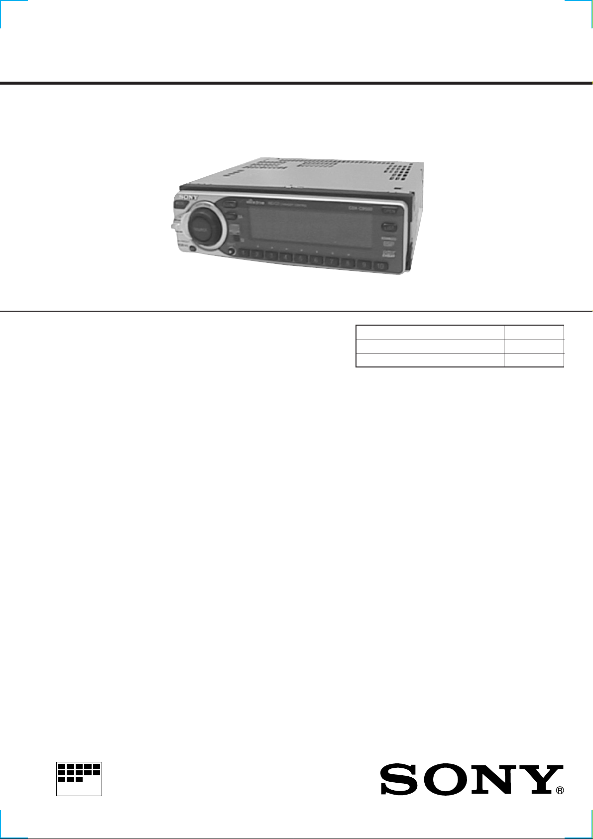
CDX-C8850/C9500
SERVICE MANUAL
Photo: CDX-C9500
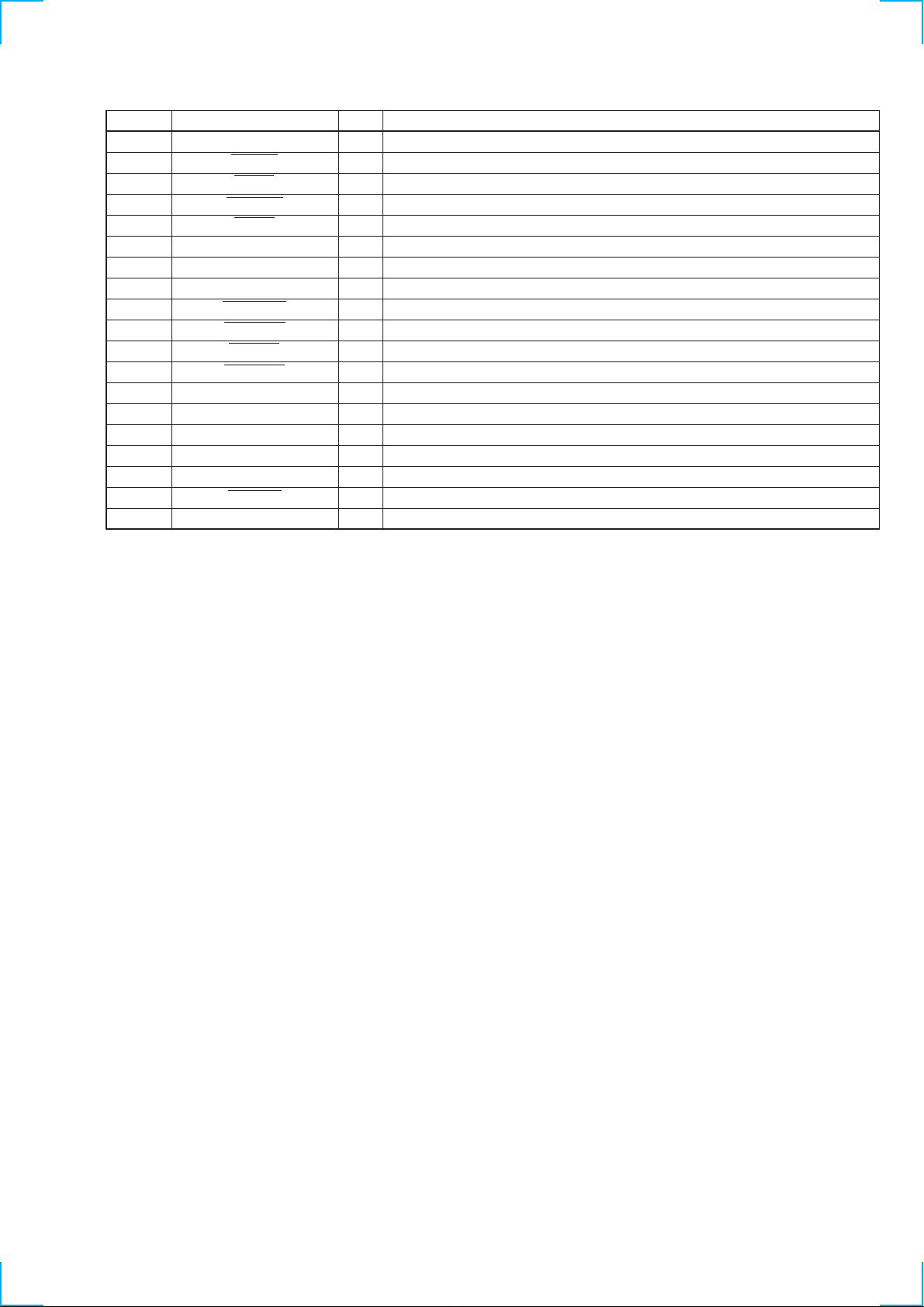
SPECIFICATIONS
AUDIO POWER SPECIFICATIONS (US Model)
POWER OUTPUT AND TOTAL HARMONIC DISTORTION
19 watts per channel minimum continuous average power into
4 ohms, 4 channels driven from 20 Hz to 20 kHz with no more
than 1% total harmonic distortion.
US Model
CDX-C8850
E Model
CDX-C9500
Model Name Using Similar Mechanism CDX-C880
CD Drive Mechanism Type MG-363S-121
Optical Pick-up Name KSS-521A
Other Specifications
CD player section
System Compact disc digital audio
system
Signal-to-noise ratio 98 dB
Frequency response 10 – 20,000 Hz
Wow and flutter Below measurable limit
Laser Diode Properties
Material GaAlAs
Wavelength 780 nm
Emission Duration Continuous
Laser output power Less than 44.6 µW*
* This output is the value measured at a distance
of 200 mm from the objective lens surface on
the Optical Pick-up Block.
Tuner section
FM
Tuning range CDX-C8850:
87.5 – 107.9 MHz
CDX-C9500:
FM tuning interval:
50 kHz/200 kHz switchable
87.5 – 108.0 MHz
(at 50 kHz step)
87.5 – 107.9 MHz
(at 200 kHz step)
Antenna terminal External antenna connector
Intermediate frequency 10.7 MHz
Usable sensitivity 8 dBf
Selectivity 75 dB at 400 kHz
50 dB at 200 kHz
Signal-to-noise ratio 65 dB (stereo),
68 dB (mono)
Harmonic distortion at 1 kHz
0.7% (stereo),
0.4% (mono)
Separation 35 dB at 1 kHz
Frequency response 30 – 15,000 Hz
AM
Tuning range CDX-C8850:
530 – 1,710 kHz
CDX-C9500:
AM tuning interval:
9 kHz/10 kHz switchable
531 – 1,602 kHz
(at 9 kHz step)
530 – 1,710 kHz
(at 10 kHz step)
Antenna terminal External antenna connector
Intermediate frequency 10.71 MHz/450 kHz
Sensitivity 30 µV
Power amplifier section
Outputs Speaker outputs
(sure seal connectors)
Speaker impedance 4 – 8 ohms
Maximum power output 45 W × 4 (at 4 ohms)
– Continued on next page –
FM/AM COMPACT DISC PLAYER
MICROFILM
1
Page 2
SECTION 4
DIAGRAMS
4-1. IC PIN DESCRIPTIONS
• IC501 CXD2548R (DIGITAL SERVO, DIGITAL SIGNAL PROCESSOR) (SERVO BOARD)
Pin No. Pin Name I/O Pin Description
1 SYSM I System mute input (Not used.)
2 RMUT1 O R-ch, “0” detection output. (“H” : ON, “L” : OFF) (Not used.)
3 LMUT2 O L-ch, “0” detection output. (“H” : ON, “L” : OFF) (Not used.)
4 CKOUT O Master clock frequency division output (Not used.)
5 VDD0 — Digital power supply
6 SBSO O Serial output of sub-P to W.
7 EXCK I Clock input for SBSO read output.
8 SQCK I Clock input for SQSO read output.
9 SQSO O SubQ 80 bit, PCM peak and level data 16 bit output.
10 SENS O SENS output. Output to CPU.
11 SCLK I Clock input for SENS real data read.
12 DATA I Serial data input from CPU.
13 XLAT I Latch input from CPU. Latch serial data at the falling edge.
14 CLOK I Serial data transfer clock input from CPU.
15 XRST I System reset (“L” : Reset)
16 ACDT O Not used.
17 PWM1 I External control input of spindle motor.
18 XLON O Microcomputer extension interface (Output) (Not used.)
19 SPOA I Microcomputer extension interface (Input A) (Not used.)
20 WFCK O WFCK (Write Flame Clock) output
21 GTOP O GTOP output
22 XUGF O XUGF output (Not used.)
23 XPCK O XPLCK output (Not used.)
24 GFS O GFS output
25 RFCK O RFCK output
26 C2PO O C2PO output (Not used.)
27 XROF O XROF output
28 SCOR O “H” output at either detection, sub code sync S0 or S1.
29 MNT0 O MNT0 output (Not used.)
30 MNT1 O MNT1 output (Not used.)
31 MNT3 O MNT3 output (Not used.)
32 VSS1 — Digital GND
33 DOUT O Digital-Out output
34 ATSK I For anti-shock.
35 MIRR O Mirror signal output (Not used.)
36 DFCT O Diffect signal output (Not used.)
37 FOK O Focus OK signal output
38 VDD1 — Digital power supply
39 VPCO1 O Charge pump output for wideband EFM PLL.
40 VPCO2 O VCO2 charge pump output for wideband EFM PLL.
41 VCK.I I VCO2 oscillator input for wideband EFM PLL.
42 V16M O VCO2 oscillator output for wideband EFM PLL.
43 VCTL I VCO2 control input for wideband EFM PLL.
44 PCO O Charge pump output for master PLL.
45 FILO O Filter output for master PLL (slave = digital PLL).
46 FILI I Filter input for master PLL.
47 AVSS4 — Analog GND
48 CLTV I VCO control voltage input for master.
49 AVDD4 — Analog power supply
50 RFAC I EFM signal input
51 BIAS I Asymmetry circuit constant current input
23
Page 3
Pin No. Pin Name I/O Pin Description
52 ASY.I I Asymmetry comparate voltage input
53 ASY.O O EFM full-swing output (“L” : VSS, “H” : VDD)
54 VC I Center voltage input
55 FE I Focus error signal input
56 SE I Sled error signal input
57 TE I Tracking error signal input
58 CE I Center error signal input
59 RFDC I RF signal input
60 RFC I Condenser connection pin for LPF time constant of RF signal.
61 ADIO O OP amplifier output (Not used.)
62 AVSS3 — Analog GND
63 IGEN I Current source reference resistor connection for OP amplifier.
64 AVDD3 — Analog power supply
65, 66 TES2, 3 I TEST pin (Fixed at “L”.)
67 VSS2 — Digital GND
68 TEST I TEST pin (Fixed at “L”.)
69 SFDR O Sled drive output
70 SRDR O Sled drive output
71 TFDR O Tracking drive output
72 TRDR O Tracking drive output
73 FFDR O Focus drive output
74 FRDR O Focus drive output
75 VDD2 — Digital power supply
76 COUT O Track number count signal output (Not used.)
77 LOCK O Not used.
78 MDS O Servo control output of spindle motor. (Not used.)
79 MDP O Servo control output of spindle motor.
80 SSTP I Disc most inner track detection signal input
81 FSTO O 2/3 frequency division output of pins 103 and 104.
82 FSTI I Reference clock input for digital servo.
83 XTSL I X’tal select input (“L” : 16.9344 MHz)
84 C4M O 4.2336 MHz output
85 WDCK O D/A interface. Word clock f = 2Fs
86 VDD3 — Digital power supply
87 LRCK O D/A interface. LR clock f = Fs
88 LRCKI I LR clock input to DAC. (48 bit slot) (Connect to GND.)
89 PCMD O D/A interface. Serial data (2’s COMP, MSB first)
90 PCMDI I Audio data input to DAC. (48 bit slot) (Connect to GND.)
91 BCK O D/A interface. Bit clock
92 BCKI I Bit clock input to DAC. (48 bit slot) (Connect to GND.)
93 EMPH O Not used.
94 EMPHI I De-emphasis ON/OFF of DAC. (“H” : ON, “L” : OFF) (Connect to GND.)
95 VSS3 — Digital GND
96 AVSS1 — L-ch, Analog GND.
97 AVDD1 — L-ch, Analog power supply.
98 AOUT1 O L-ch, Analog output. (Not used.)
99 AIN1 I L-ch, OP amplifier input. (Connect to GND.)
100 LOUT1 O L-ch, LINE output. (Not used.)
101 A VSS1 — L-ch, Analog GND.
102 XVDD — Analog power supply for master clock.
103 XTAI I X’tal oscillator input of master clock (16.9344 MHz).
104 XTAO O X’tal oscillator output of master clock. (Not used.)
105 XVSS — Analog GND for master clock. (Connect to GND.)
24
Page 4

Pin No. Pin Name I/O Pin Description
106 A VSS2 — R-ch, Analog GND.
107 ROUT2 O R-ch, LINE output. (Not used.)
108 AIN2 I R-ch, OP amplifier input. (Connect to GND.)
109 AOUT2 O R-ch, Analog output. (Not used.)
110 AVDD2 — R-ch, Analog power supply.
111 A VSS2 — R-ch, Analog GND.
112 VSS0 — Digital GND
25
Page 5
• IC5 CXP84640-050Q (CD SYSTEM CONTROL) (SERVO BOARD)
Pin No. Pin Name I/O Pin Description
1 – 5 NCO — Not used in this set.
6 FP OPEN I Front panel open detection input
7 FP CLOSE O Front panel close control output
8 LINKOFF I Bus interface link input (Not used in this set.)
9 DRV OE O Focus/tracking coil/sled motor control output
10 D SW I Down switch input (SW4)
11 – 13 NCO — Not used in this set.
14 LM EJ O Loading motor control output
15 LM LOD O Loading motor control output
16 EMPH O O De-emphasis ON/OFF control output
17 CDMON O CD mechanism deck power control output
18 CD ON O CD power control output
19 A MUT O System attenuate control output
20 LD ON O Laser power ON/OFF control output
21 CD RST O CD system reset output
22 – 24 — — Not used in this set.
25 PH3 I Not used in this set.
26 TSTIN0 I Not used in this set.
27 TSTIN1 I Not used in this set.
28 TST CLV I Not used in this set.
29 NCO — Not used in this set.
30 RESET I System reset input (“L” = Reset)
31 X IN I X’tal oscillator input of system clock. (10 MHz)
32 X OUT O X’tal oscillator output of system clock. (10 MHz)
33 GND — Analog GND
34 XT OUT O Not used in this set.
35 XT IN I Not used in this set.
36 AVSS — A/D converter GND
37 AVREF I A/D converter reference voltage input
38 TEP L I Not used in this set.
39 TEP H I Not used in this set.
40 NCO — Not used in this set.
41 PH2 I Not used in this set.
42 SCLK O CD-TEXT data read clock output
43 ESPXQOK O XQOK signal output to DRAM controller.
44 ESPSDT I Serial data input from DRAM controller.
45 GRSRST O Reset signal output to DRAM controller.
46 GRSCOR I Sub-cord sync input from DRAM controller.
47 CD XLAT O CD signal process serial latch output
48 TX CLK O EEPROM serial clock output
49 TX DATA O EEPROM serial data output
50 UNISO O Not used in this set.
51 BUS CLK I/O Bus system serial clock input/output
52 BUS SI I Bus system serial interface input
53 BUS SO O Bus system serial interface output
54 F OK I Focus OK signal input
55 GFS I GFS signal detection input
56 SCOR O Sub-cord sync output
57 SENS I SENS signal input
58 — I Fixed at “H” in this set.
59 CD CKO O CD signal process serial clock output
26
Page 6
Pin No. Pin Name I/O Pin Description
60 BU.IN I Back-up power detection input
61 BUSON I Bus on control input
62 IN SW I Disc in switch input (SW1)
63 SELF SW I Self switch input (SW2)
64 TX CE O EEPROM chip enable output
65 SCK2 O Sub Q read clock output
66 SI2 I Sub Q 80 bit, PCM peak and level data 16 bit input
67 CD DATA O CD signal process serial data output
68 ESPXWRE O Write signal output to DRAM controller.
69 ESPXRDE O Read signal output to DRAM controller.
70 ESPXLT O Serial data latch output to DRAM controller.
71 ESPXSOE O XSOE signal output to DRAM controller.
72 VDD — Power supply
73 HIN I Fixed at “H” in this set.
74 TEXT.ON/OFF I Fixed at “H” in this set.
75 PH1 I Not used in this set.
76 FBTBSEL I Not used in this set.
77 CDOSEL I Not used in this set.
78 – 80 — — Not used in this set.
27
Page 7
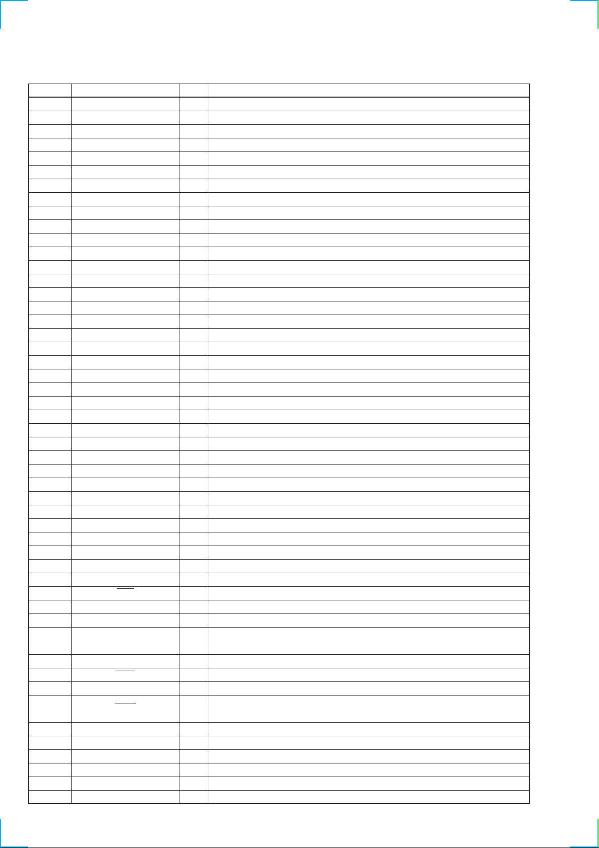
• IC300 CXD2727Q (DIGITAL SIGNAL PROCESSOR) (MAIN BOARD)
Pin No. Pin Name I/O Pin Description
1 VSS1 — Digital ground
2 – 15 TD0 – 13 I Test pin (Normally, fixed at “L”.)
16 – 21 TST0 – 5 I Test pin (Normally, fixed at “L”.)
22 – 24 JPE1 – 3 I External condition jump input (“H” : condition jump) (Fixed at “L” in this set.)
25 VDD1 — Digital power supply pin (+3.3 V)
26 AVS3 — Analog ground (for D/A converter 1)
27 FL-OUT O Analog signal output for front (L-ch) output.
28 AVD3 — Analog power supply pin (+3.3 V) (for D/A converter 1)
29 RL-OUT O Analog signal output for rear (L-ch) output.
30 AVD5 — Analog power supply pin (+3.3 V) (for D/A converter 1)
31 AVS5 — Analog ground (for D/A converter 1)
32 AVD1 — Analog power supply pin (+3.3 V) (for A/D converter L-ch)
33 AVS1 — Analog ground (for A/D converter L-ch)
34 LREF O Pass control connection pin for A/D converter. (for L-ch)
35 LIN I Tuner and bus audio in signal input (for L-ch)
36 AVS7 — Analog ground (for D/A converter 2)
37 AVD7 — Analog power supply pin (+3.3 V) (for D/A converter 2)
38 NCO — Not used. (Open)
39 AVDX — Analog power supply pin (+3.3 V) (for master clock)
40 XTLO38 O System clock output (16.9344 MHz)
41 XTLI38 I System clock input (16.9344 MHz)
42 AVSX — Analog ground (for master clock)
43 SUB-OUT O Analog signal output for sub woofer output.
44 AVD8 — Analog power supply pin (+3.3 V) (for D/A converter 2)
45 AVS8 — Analog ground (for D/A converter 2)
46 RIN I Tuner and bus audio in signal input (for R-ch)
47 RREF O Pass control connection pin for A/D converter. (for R-ch)
48 AVS2 — Analog ground (for A/D converter R-ch)
49 AVD2 — Analog power supply pin (+3.3 V) (for A/D converter R-ch)
50 AVS6 — Analog ground (for D/A converter 3)
51 AVD6 — Analog power supply pin (+3.3 V) (for D/A converter 3)
52 RR-OUT O Analog signal output for rear (R-ch) output.
53 AVD4 — Analog power supply pin (+3.3 V) (for D/A converter 3)
54 FR-OUT O Analog signal output for front (R-ch) output.
55 AVS4 — Analog ground (for D/A converter 3)
56 VSS2 — Digital ground
57 RST I System reset signal input from system control (IC500). (“L” : reset)
58 BFOT O Master clock output for CD.
59 SCK I Clock signal input for serial data transfer from system control (IC500).
60 REDY O
61 TRDT O Serial data output to system control (IC500).
62 LAT I Serial data latch pulse input from system control (IC500).
63 RVDT I Serial data input from system control (IC500).
64 XS24 I
65 VDD2 — Digital power supply pin (+3.3 V)
66 VSS3 — Digital ground
67 – 69 SO1 – 3 O Serial data output (Not used in this set.)
70 SOUT O Serial data output (Not used in this set.)
71 SI1 I Serial data input
72, 73 SI2, 3 I Serial data input (Fixed at “L” in this set.)
Micon interface transfer permission signal output to system control (IC500).
(“L” : transfer prohibit)
Serial data 24/32 bit slot select signal input from system control (IC500).
(“L” : 24 bit slot, “H” : 32 bit slot) (Valid at slave mode.)
28
Page 8

Pin No. Pin Name I/O Pin Description
74 SIN I Serial data input (Fixed at “L” in this set.)
75 BCK I Clock signal input for serial bit transfer of serial input/output data.
76 LRCK I Sampling frequency clock signal input of serial input/output data.
77 XMST I
78 VDD3 — Digital power supply pin (+3.3 V)
79 AVSP — PLL system ground
80 PLLEN I PLL enable signal input (Normally, fixed at “L”.)
81 PLCLK O PLL clock signal output (Not used in this set.)
82 CKSTP I PLL clock output control signal input from system control (IC500).
83 AVDP — PLL system power supply pin (+3.3 V)
84 VSS4 — Digital ground
85 – 94 TD14 – 23 I Test pin (Normally, fixed at “L”.)
95 VDD4 — Digital power supply pin (+3.3 V)
96 AVSD — Ground (for D-RAM)
97 SCLI I Not used. (Normally, fixed at “L”.)
98 BIM I Not used. (Normally, fixed at “L”.)
99 SDRAM I Not used. (Normally, fixed at “L”.)
100 AVDD — Power supply pin (+3.3 V) (for D-RAM)
Bit clock (BCK) and L/R sampling clock (LRCK) signal master/slave mode select
signal input from system control (IC500). (“L” : master mode, “H” : slave mode)
29
Page 9
• IC701 HD6432355A08F (DISPLAY CONTROL) (MAIN BOARD)
Pin No. Pin Name I/O Pin Description
1, 2 PG3, 4 O Not used. (Open)
3 VSS — Ground
4 NC — Not used. (Open)
5 VCC — Power supply pin (+5 V)
6 – 9 PC0 – 3 O Not used. (Open)
10 VSS — Ground
11 – 14 PC4 – 7 O Not used. (Open)
15 – 18 PB0 – 3 O Not used. (Open)
19 VSS — Ground
20 – 23 PB4 – 7 O Not used. (Open)
24 – 27 PA0 – 3 O Not used. (Open)
28 VSS — Ground
29 PA4/IRQ4 O Not used. (Open)
30 PA5/IRQ5 O Not used. (Open)
31 PA6/IRQ6 O Not used. (Open)
32 PA7/IRQ7 O Not used. (Open)
33 SP-LAT I Digital signal processor spectrum analyzer data latch input
34 P66/IRQ2 O Not used. (Open)
35, 36 VSS — Ground
37 P65/IRQ1 O Not used. (Open)
38 BUS-ON I SONY BUS ON input
39 VCC — Power supply pin (+5 V)
40 CD/MD I CD/MD mechanism deck setting input (“L” : CD mechanism deck)
41 – 43 PE1 – 3 O Not used. (Open)
44 VSS — Ground
45 TIR IND O TIR indicator LED drive output
46, 47 PE5, 6 O Not used. (Open)
48 MD LOCK I MD lock signal input (“L” : unlock)
49 BU-IN I Back-up power supply detection input
50 LINK-OFF O LINK OFF output (Not used in this set.)
51 PD2 O Not used. (Open)
52 ILL-ON O Illumination power supply control output
53 VSS — Ground
54 DOOR SW I DOOR switch input (“L” : close, “H” : open)
55 NCO — Not used. (Open)
56 PD6 O Not used. (Open)
57 BOOT I FLASH write mode detection input
58 VCC — Power supply pin (+5 V)
59 NC — Not used. (Open)
60 TX/FL-SO/LCDDATA O LCD driver serial data/FLASH rewriting serial data output
61 SP-SI I Digital signal processor spectrum analyzer data input
62 RX I FLASH rewriting serial data input
63 SP-SCK I Digital signal processor spectrum analyzer data serial clock input
64 LCDCLK O LCD driver/serial clock output
65 VSS — Ground
66 LCDINH O LCD driver inhibit control output
67, 68 VSS — Ground
69 LCDCE0 O LCD chip enable output
70 LCDCE1 O LCD chip enable output
71 P63 O Not used. (Open)
72 – 78 P27 – 21 O Not used. (Open)
79 FL W O FLASH write control output
30
Page 10

Pin No. Pin Name I/O Pin Description
80 FWE (L) I FLASH write enable input
81 RES I Reset input
82 NMI (H) I Non-maskable interruption input
83 STBY (H) I Hardware standby input
84 VCC — Power supply pin (+5 V)
85 XTAL I Main clock crystal input (18.432 MHz)
86 EXTAL O Main clock crystal output (18.432 MHz)
87 VSS — Ground
88 PF7 O Not used. (Open)
89 VCC — Power supply pin (+5 V)
90 – 96 PF6 – 0 O Not used. (Open)
97 UNI-SO O SONY BUS serial data output
98 UNI-SI I SONY BUS serial data input
99, 100 VSS — Ground
101 UNI-SCK I SONY BUS serial clock input
102 P53/ADTRG O Not used. (Open)
103 AVCC — A/D, D/A power supply pin (+5 V)
104 VREF — A/D, D/A reference voltage input (+5 V)
105 P40/AN0 I Not used. (Connect to ground.)
106 P41/AN1 I Not used. (Connect to ground.)
107 P42/AN2 I Not used. (Connect to ground.)
108 P43/AN3 I Not used. (Connect to ground.)
109 P44/AN4 I Not used. (Connect to ground.)
110 P45/AN5 I Not used. (Connect to ground.)
111 P46/AN6/DA0 I Not used. (Connect to ground.)
112 P47/AN7/DA1 I Not used. (Connect to ground.)
113 AVSS — A/D, D/A ground
114 VSS — Ground
115 – 122 P17 – 10 O Not used. (Open)
123 MD0 (H) I Operation mode setting input (Fixed at “H”.)
124 MD1 (H) I Operation mode setting input (Fixed at “H”.)
125 MD2 (H) I Operation mode setting input (Fixed at “H”.)
126 – 128 PG0 – 2 O Not used. (Open)
31
Page 11

• IC500 MB90574APMT-G-214-BND (SYSTEM CONTROL) (MAIN BOARD)
Pin No. Pin Name I/O Pin Description
1, 2 RE IN0, 1 I Rotary encoder input
3 TIR BUSY O Not used. (Open)
4 TIR PDOWN O Not used. (Open)
5 TIR RST O Not used. (Open)
6 SYS RST O Reset output for SONY BUS slave micon.
7 BUS ON O SONY BUS ON output
8 VCC — Power supply pin (+5 V)
9 DSPSTP O Digital signal processor master clock control output
10 TIR PLAY O Not used. (Open)
11 CSV PLAY O Voice guide sound/Digital signal processor sound select output
12 RX/FLS SI I FLASH write communication input
13 TX/FLS SO O FLASH write communication output
14 FLS WR I FLASH write mode select input
15 BEEP O Beep output
16 CSV ON O CSV control IC power supply control output
17 DSP SI I Serial data input from digital signal processor.
18 DSP SO O Serial data output to digital signal processor.
19 DSP CK O Serial data shift clock output to digital signal processor.
20 UNI SI I SONY BUS serial data input
21 UNI SO O SONY BUS serial data output
22 UNI CK O SONY BUS serial clock output
23 SD IN I Tuner reception signal detection input
24 SIRCS I Wireless remote commander signal input
25 CSV SI I CSV control IC serial data input
26 CSV SO O CSV control IC serial data output
27 CSV CK O CSV control IC serial clock output
28 DSP RST O Digital signal processor reset output
29 ST/MONO I/O Used in conjunction with stereo input/forced monaural output.
30 DSP XMST O Digital signal processor master mode/slave mode select output
31 WIDE O WIDE/NARROW select output
32 NARROW O WIDE/NARROW select output
33 VSS — Ground
34 C — Stabilized capacitor connection pin
35 RAM BU I RAM backup voltage detection input
36 MUTE O Mute control output of audio output.
37 ASEL0 O Digital signal processor analog input source select output
38 DVCC — D/A power supply pin (+5 V)
39 DVSS — D/A ground
40 ASEL1 O Digital signal processor analog input source select output
41 LCD ANG O LCD contrast alignment output
42 AVCC — D/A, A/D power supply pin (+5 V)
43 AVRH — A/D reference voltage input (+5 V)
44 AVRL — A/D reference voltage input (0 V)
45 A VSS — D/A, A/D ground
46 VSM I Tuner S-Meter voltage input
47, 48 KEY IN0, 1 I Front panel key input
49 RC IN0 I Rotary commander key input
50 DST SEL0 I Destination select input (“L” : C9500, “H” : C8850)
51 DST SEL1 I Destination select input
52 QUALITY I Tuner quality voltage input
53 MPT I Tuner multi pass voltage input
54 VCC — Power supply pin (+5 V)
32
Page 12

Pin No. Pin Name I/O Pin Description
55 VOL LOAD O Electronic volume IC data latch output
56 VOL DATA L O Electronic volume L-ch setting data output
57 VOL DATA R O Electronic volume R-ch setting data output
58 VOL CLK O Electronic volume setting clock output
59 DSP XLAT O Data latch output to digital signal processor.
60 RC IN1 I Rotary commander shift switch input
61 ACC IN I Accessory signal input
62 POW ON O System power ON/OFF control output
63 VSS — Ground
64 BOOT O Low output at display micon rewriting.
65 PWM I PWM control input
66 NCO — Not used. (Open)
67 RDS DAVN I RDS IC data reception mode read input
68 CD/MD I CD/MD mechanism deck setting input (“L” : CD mechanism deck)
69 CD/MD ON I CD/MD servo B+ detection input
70 I2C SDA I/O For communication with device connected to I2C-bus.
71 I2C SCL I/O For communication with device connected to I2C-bus.
72 SHIFT O Shift signal output
73 X1A O Low speed frequency output (32.768 kHz)
74 X0A I Low speed frequency input (32.768 kHz)
75 NCO — Not used. (Open)
76 KEY ACK I Key input detection at micon sleeping.
77 BU IN I Back-up power supply detection input
78 SP LAT O Spectrum analyzer data latch output
79 DSP REDY I Ready signal input from digital signal processor.
80 TEST I Test input
81 EMPH I Emphasis signal input at MD/CD play. (“H” : emphasis ON)
82 WAKE UP O DC/DC converter power supply ON/OFF control output (Not used in this set.)
83 TEL MUTE I Audio signal muting input (“L” : mute ON)
84 TU ON O Tuner power supply ON/OFF output
85 ILL IN I Illumination signal input
86 HSTX I Hardware standby input
87 MD2 I Operation mode designation input (Fixed at “L” in this set.)
88, 89 MD1, 0 I Operation mode designation input (Fixed at “H” in this set.)
90 RST I Reset input
91 VSS — Ground
92 X0 I High speed frequency input (3.68 MHz)
93 X1 O High speed frequency output (3.68 MHz)
94 VCC — Power supply pin (+5 V)
95 DOOR IND O Front panel door indicator output
96 DSP ON O Digital signal processor power control output
97 NCO — Not used. (Open)
98 AMP-STBY O Power amplifier standby signal output
99 – 102 TIR D0 – 3 O Not used. (Open)
103 TIR RD O Not used. (Open)
104 TIR WR O Not used. (Open)
105 TIR CE1 O Not used. (Open)
106 TIR CE0 O Not used. (Open)
107 AD ON O Power control output to keys.
108 NCO — Not used. (Open)
109 NOSE SW I Front panel attachment detection input
110 CSV REQ I Data transfer request input from CSV control IC.
111 CSV CE O Chip enable output to CSV control IC.
33
Page 13

Pin No. Pin Name I/O Pin Description
112 CSV RST O CSV control IC initial reset output
113 NCO — Not used. (Open)
114 FM ON O Power control output at FM reception.
115 DOOR SW I Door switch input
116 NS MASK O Mask control output of quality input at tuner reception.
117 SEEK O Seek control output at tuner reception.
118 AF MUTE O Muting output of tuner audio output.
119 VSS — Ground
120 SSTOP I IF count result input of PLL IC.
34
Page 14

4-6. SCHEMATIC DIAGRAM — CD MECHANISM SECTION (1/3) — • Refer to page 57 for IC Block Diagrams.
CDX-C8850/C9500
(Page 40)
Note:
• Voltage and waveforms are dc with respect to ground
under no-signal conditions.
no mark : CD PLAY
: Impossible to measure
∗
(Page 41)
39 39
Page 15

CDX-C8850/C9500
4-7. SCHEMATIC DIAGRAM — CD MECHANISM SECTION (2/3) — • Refer to page 57 for IC Block Diagrams.
(Page 39)
(Page 41)
40 40
Note:
• Voltage and waveforms are dc with respect to ground
under no-signal conditions.
no mark : CD PLAY
: Impossible to measure
∗
Page 16

4-8. SCHEMATIC DIAGRAM — CD MECHANISM SECTION (3/3) — • Refer to page 58 for IC Block Diagrams.
CDX-C8850/C9500
(Page 39)
(Page 40)
(Page 49)
41 41
Note:
• Voltage and waveforms are dc with respect
to ground under no-signal conditions.
no mark : CD PLAY
: Impossible to measure
∗
Page 17

CDX-C8850/C9500
4-11. SCHEMATIC DIAGRAM — MAIN SECTION (1/5) — • Refer to page 59 for IC Block Diagrams.
(Page 49)(Page 47)
46 46
Note:
• Voltage is dc with respect to ground under no-signal
(detuned) condition.
no mark : FM
(): AM
Page 18

4-12. SCHEMATIC DIAGRAM — MAIN SECTION (2/5) — • Refer to page 59 for IC Block Diagrams.
(Page 46)
CDX-C8850/C9500
(Page 49)
(Page 48)
(Page 50)
47 47
Note:
• Voltage is dc with respect to ground under no-signal
(detuned) condition.
no mark : FM
Page 19

CDX-C8850/C9500
4-13. SCHEMATIC DIAGRAM — MAIN SECTION (3/5) — • Refer to page 60 for IC Block Diagrams.
(Page 47)
(Page 49)
(Page 50)
Note:
• Voltage is dc with respect to ground under no-signal
(detuned) condition.
no mark : FM
48 48
Page 20

4-14. SCHEMATIC DIAGRAM — MAIN SECTION (4/5) — • Refer to page 60 for IC Block Diagrams.
CDX-C8850/C9500
(Page 41)
(Page 46)
(Page 47)
(Page 48)
(Page 50)
(Page 47)
(Page 51)
(Page 50)
49 49
Note:
• Voltage is dc with respect to ground under no-signal
(detuned) condition.
no mark : FM
Page 21

CDX-C8850/C9500
4-15. SCHEMATIC DIAGRAM — MAIN SECTION (5/5) — • Refer to page 59 for IC Block Diagrams.
(Page 48)(Page 47)
(Page 49)
(Page 54)
50 50
Note:
• Voltage is dc with respect to ground under no-signal
(detuned) condition.
no mark : FM
Page 22

4-16. SCHEMATIC DIAGRAM — POWER SECTION — • Refer to page 60 for IC Block Diagrams.
(Page 49)
CDX-C8850/C9500
51 51
Note:
• Voltage is dc with respect to ground under no-signal
(detuned) condition.
no mark : FM
Page 23

CDX-C8850/C9500
4-19. SCHEMATIC DIAGRAM — RELAY SECTION —
(Page 55)
(Page 50)
54 54
Page 24

4-20. SCHEMATIC DIAGRAM — DISPLAY SECTION —
(Page 54)
CDX-C8850/C9500
55 55
Note:
• Voltage is dc with respect to ground under no-signal
(detuned) condition.
no mark : FM
Page 25

+–
+–
+
–
1
OPOUT
20
GND
25
OPIN–24OPIN+
2NC3NC4
BIAS
5
DRIN'
6
DRIN
23NC22
MUTE21NC
DRIVER
MUTE
7NC8NC9NC10NC11NC12
+–
13
LEVEL SHIFT
IN
+–
THERMAL
SHUT DOWN
19
GND
14
NC
18NC16NC15
NC
VCC
17
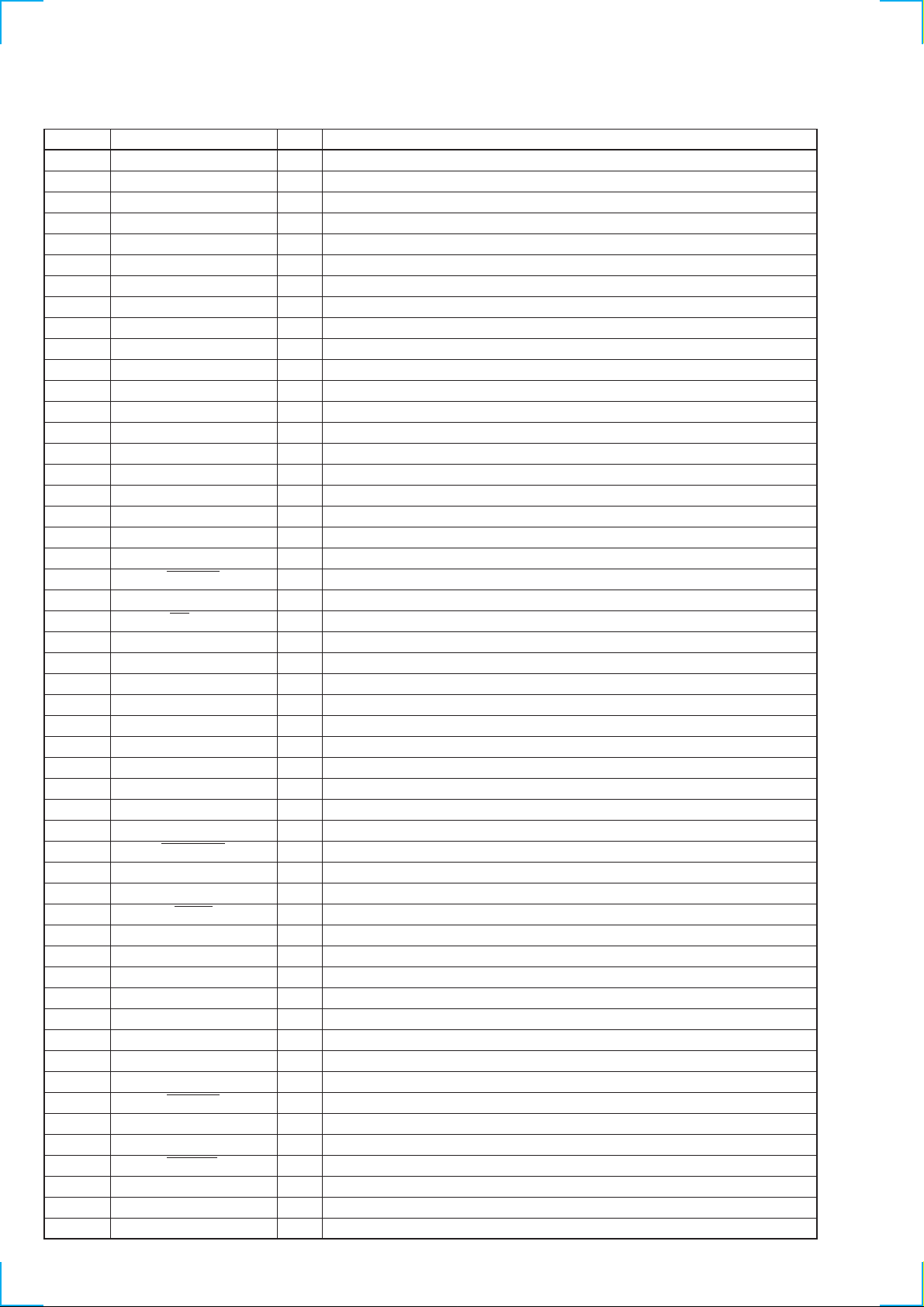
• IC Block Diagrams
IC1 CXA1791N-T4
1
LD
APC
PD AMP
+
–
–
+
VC
RF
IV AMP1
–
+
VC
RF
IV AMP2
–
+
VC
VC
VC
F
IV AMP
–
+
E
IV AMP
PD1
PD2
GND
2
PD
3
4
5
6
F
7
E
8
VR
9
VC
10
NC
VREF
1.25V
APC
LD AMP
+
–
VC
VC
VC BUFFER
IC601 BA6195FP-YT2
VC
VCC
–
+
VC
SUMMING AMP
–
+
FOCUS
ERROR AMP
VC
VC
–
VC
+
–
+
VCC
TRACKING
ERROR AMP
20
VCC
19
APC ON
18
RFI
17
16
15
14
13
12
11
RFO
FE
FE BIAS
TE
EI
EO
NC
IC6 LB1638MTP-T1
1
GND
2
IN1
VCC
IN2
3
4
CONTROL LOGIC
10
N.C.
9
OUT1
VS
8
7
OUT2
RF
IC7 BA6797FP-E2
GND
28
LEVEL SHIFT
VCC/2 VCC/2
GND
PRE-
OUT4-A
OUT4-B
27
VCC/2 VCC/2 VCC/2 VCC/2
–
+
LEVEL
–
+
IN
SHIFT
IN
PRE-
OUT4
242526
IN4 (+)
IN4 (–)
23
VCC
VCC
VCC
22
20
21
VCC
IN3(+)
19
IN3(–)
OUT3
IN
LEVEL
OUT3-B
161718
+–
SHIFT
LEVEL
IN
VCC/2 VCC/2
5 6
OUT3-A
GND
15
SHIFT
+–
N.C.
1
23
OUT1-A
OUT1-B
PRE-
OUT1
4
IN1 (–)
5
IN1 (+)
6
789101112 13
REG-B
REG-
OUT
BIAS-
IN
MUTE
IN2 (+)
IN2 (–)
PRE-
OUT2
OUT2-B
14
OUT2-A
57
Page 26

IC4 MB814400C-70PFTN
DQ1
1
DQ2
2
WE
RAS
3
GENERATOR
4
CLOCK
1
WRITE
CLOCK
GENERATOR
CLOCK
GENERATOR
2
CONTROL
MODE
DATA INPUT
BUFFER
COLUMN
DECODER
SENSE AMP
I/O GATE
ADDRESS
BUFFER
DATA OUTPUT
BUFFER
4M BIT
MEMORY
CELL
ROW
DECODER
PRE-
DECODER
BOARD
GENERATOR
REFRESH
ADDRESS
COUNTER
BIAS
IC551 LC89170M-TLM
VSS
26
25
DQ4
DQ3
24
EXCK
1
2
SBSO
3
SCOR
CAS
23
OE
22
WFCK
4
5
MCK
6
XMODE
7
GND
32 WORD X 8 BIT
DUAL PORT RAM
CPU INTERFACE
TIMING
&
SYNCHRONIZATION
SIGNAL
PROTECTION
CRC
CHECKER
VDD
14
VDD
13
DQSY
SRDT
12
11
SCLK
10
SW2
SW1
9
8
TEST
A9
5
A0
9
A1
10
A2
11
A3
12
VCC
13
IC2 CXD2522R-T6
49
XEMP
50
XWIH
AM4
51
AM3
52
53
AM2
54
AM1
55
AM0
56
VDD
57
XQOK
XSOE
SDTO
47
48
READ
BASE
COUNTER
46
XRDE
SDTI
XLT
SCK
ADDRESS MONITOR
CPU I/F
WRITE
BASE
COUNTER
XWRE
42434445
SPSL
VWA
A8
18
A7
17
A6
16
15
A5
A4
14
A5
36
DRAM
I/F
A8
A6
A7
XOE
35
33
34
32
XCAS
31
D4
30
D3
29
D0
28
D1
27
XWE
XRAS
26
25
A9
24
VDD
23
A0
22
A1
21
A2
20
A3
OSCE
VSS
4041
A4
3739
38
GSCR
SCOR
GRST
XRST
58
SELECTOR
58
59
NC
60
NC
61
NC
62
63
64
DATA
LINKING
CONTROL
12
456 789
3
DIN
C4M
XROI
WFCK
RFCK
GTOP
DSP
I/F
10 11 13
VSS
DATI
LRCI
BCKI
WDCI
TEST
XTAO
TIMING
GEN.
DAC
I/F
15
1612
14
BCK
XTAI
DATA
DIGITAL
OUT
19
C176
18
DOUT
17
LRCK
Page 27

IC151 TDA7427ADTR
1
5
2
4
3
IN B
VCC
IN A
GND
OUT Y
LP OUT
11 BIT
PROGRAMMABLE
COUNTER
SWITCH
OUT
INLOCK
CHARGE
PUMP
DETECTOR
PARATOR
+
–
SWITCH
LP1/LP2
3 41 2 785 6 11 129
VREF
LP HC
LP FM
LP AM
PHASE
COM-
SWITCH
SWM/DIR
5 BIT
PROGRAMMABLE
COUNTER
PRE
COUNTER
SWITCH
SWM/DIR
16 BIT
PROGRAMMABLE
COUNTER
TEST
LOGIC
PORT
EXTENSION
DOUT3
DOUT4
DOUT5
DOUT6
FM/AM
SWITCH
TIMER
14 BIT
PROGRAMMABLE
COUNTER
REFERENCE
OSCILLATOR
10
OSCIN
OSCOUT
VDD2
AM IN
GND-AM
NC
NC
FM IN
POWER ON RESET
11 – 21 BIT
PROGRAMMABLE
GND-SIG
SUPPLY &
CONTROL
COUNTER
VDD1
ADDR
IIC BUS
INTERFACE
SCL
DOUT1/INLOCK
HFREF
SSTOP
DOUT2
FM/AM
SWITCH
13 14
SDA
IF FM
1516171819202122232425262728
IF AM
IC551 LC89170M-TLM
EXCK
1
2
SBSO
SCOR
WFCK
MCK
XMODE
GND
3
4
5
6
7
32 WORD X 8 BIT
DUAL PORT RAM
CPU INTERFACE
TIMING
&
SYNCHRONIZATION
SIGNAL
PROTECTION
CRC
CHECKER
VDD
IC271 BA8270FV-E2
BUS ON
1
14
VDD
2
13
DQSY
SRDT
12
11
SCLK
10
SW2
SW1
9
8
TEST
RST
BATT
3
4
CLK
5
VREF
6
DATA
GND
7 8
BUS ON
SWITCH
RESET
SWITCH
BATTERY
SWITCH
14
13
12
11
10
9
VCC
RST
BUS ON
CLK IN
BU IN
DATA IN
DATA OUT
IC352 TC7SET08FU (TE85L)
59
Page 28

IC602, 632 LM1973XM IC604, 634 NJM2160AM-TE2
1
IN3
GND3
VSS1
OUT2
18
19
20 17 16
RESISTIVE
NETWORK
TAP
SWITCHES
OUT3
VDD215GND AC14VDD113DATA-OUT12DATA-IN
SWITCH
DRIVE
DECODE
11
VCCL
SVRL
INL
2
3
BUFFER
BUFFER
VCCL
LIFT
AMP
CL+
16
CL–
15
TAP
SWITCHES
RESISTIVE
NETWORK
1 2 3
GND2
IN2
DECODE
SWITCH
DRIVE
GND AC
DECODE
TAP
SWITCHES
RESISTIVE
NETWORK
4 5 6
IN1
GND1
SWITCH
DRIVE
IC507 RN5VD33AA-TL
CD
5
RESET
2 3
1
OUT
VDD
4
NC
GND
OUT1
7
VSS2
LATCH
SHIFT
REGISTER
8
9
CLOCK
LOGIC GND
10
LOAD/SHIFT
INML
INMR
SVRR
INR
VCCR
REFERENCE
4
5
REFERENCE
6
7
8
BUFFER
BUFFER
VCCL
VCCR
VCCR
SIGNAL
AMP
SIGNAL
AMP
LIFT
AMP
LGND
14
OUTL
13
12
OUTR
RGND
11
CR–
10
9
CR+
IC702 TC7W14FU (TE12R)
VCC
1A
1 7
3Y
2 6
2A
3
4
GND
8
1Y
3A
2Y
5
60
IC691, 752 TC7W66FU (TE12L)
VCC
CONT1
OUT/IN2
CONT2
OUT/IN1
IN/OUT2
4321
GND
8 7 6 5
IN/OUT1
IC804 TCTS32FU-TE85L
VCC
IN B
IN A
GND
1
2
3
5
4
OUT Y
IC802 TC74VHC08FT (EL)
8
9
10
11
12
13
14
VCC
GND
7
6
5
4
3
2
1
Page 29

IC801 RSC-164
AIN1
AIN0
AGND
BUFOUT/PWM0
TEST/PWM1
AVDD
GND
DACOUT
BUFFER
DAC
ANALOG
CONTROL
ADC
49
SH
50
ADC
MUX
51
52
53
54
55
56
D7
57
D6
58
D5
59
D4
60
D3
61
D2
62
D1
63
D0
64
DATA BUS
XML
XMH
EXTERNAL MEMORY
INTERFACE
WRD
INTERNAL ROM
32 X 8 (HIGH)
INTERNAL ROM
32 X 8 (LOW)
RDD
WRC
RDC
ADDRESS BUS
GND
VDD
P00
P01
INTERNAL BUS
INTERRUPT
LOGIC
PON
SLEEP
POWER
CONTROL
WAKEUP LOGIC
(FROM PORT 0/1)
P02
P03
PORT 0
TIMING &
CONTROL
P04
P05
33343536373839404142434445464748
REGISTER
SPACE
PULSE WIDTH
MODULATOR
P06
STACK
SPACE
TIMER
CPU
OSC
PORT 1
P07
32
P10
31
P11
30
P12
29
P13
28
P14
27
P15
26
P16
25
P17
24
VDD
23
GND
22
RESET
21
XI1
20
XO1
19
18
A0
17
A1
1
A15
A14
A13
A12
62 3 54
87 9 1410 11 1312 16
A9
A8
A11
A10
GND
A7A6A5A4A3
VDD
15
A2
IC803 MSM534001E-49TSKFDR3 (CDX-C8850)
IC803 MSM534001E-50TSKFDR3 (CDX-C9500)
OE
A10CED7D6D5D4D3
32 2731 30 2829 2526 24 1923 22 2021 1718
ADDRESS
BUFFER
VSSD2D1D0A0A1A2
X
DECODER
Y
DECODER
CE/OE
CONTROL
MEMORY CELL
MATRIX
524,288 X 8
MULTIPLEXER
OUTPUT
BUFFER
A3
1 62 3 54
A9
A11
87 9 1410 11 1312 1615
A8
A13
A14
A17
A18
VCC
NC
A16
A15
A7A6A5
A12
A4
61
Page 30

IC805 MBM29F800TA
A16
A15
1
A14
2
A13
3
A12
4
A11
5
A10
6
A9
7
A8
8
NC
9
10
NC
WE
11
RESET
12
13
NC
NC
14
RY/BY
15
A18
16
A17
17
A7
18
A6
19
A5
20
A4
21
A3
22
A2
23
A1
24 25
ADDRESS
LATCH
STB
CONTROL
CIRCUIT
RY/BY
BUFFER
X
DECODER
Y
DECODER
8,388,608
CELL
MATRIX
Y GATE
DATA
LATCH
STB
LOW VCC
DETECTOR CIRCUIT
WRITE/ERASE
PULSE TIMER
WRITE CIRCUIT
ERASE CIRCUIT
CHIP ENABLE/
OUTPUT ENABLE
CIRCUIT
I/O
BUFFER
BYTE
GND
DQ15/A–1
DQ7
DQ14
DQ6
DQ13
DQ5
DQ12
DQ4
VCC
DQ11
DQ3
DQ10
DQ2
DQ9
DQ1
DQ8
DQ0
GND
OE
CE
A0
48
47
46
45
44
43
42
41
40
39
38
37
36
35
34
33
32
31
30
29
28
27
26
IC871 TL1451ACDB-E20
REF
OUT
S.C.P
NON-INV-
INPUT2
INV-
INPUT2
VERF.
+2.5V
REFERENCE
VOLTAGE
+2.5V
SHORT
CIRCUIT
PROTECTION
COMPARATOR
+
+
–
VREF/2
TRIANGLE
OSCILLATOR
1
CT
VCC
2 3
RT
–
+
ERROR
AMP2
VERF
VERF
SR R
LATCH
U.V.L.O
4
INV-
INPUT1
NON-INV-
INPUT1
FEED
BACK2
VERF
+
–
ERROR
AMP1
5 6 7 8
FEED
BACK1
DEAD
DEAD
TIME
CONTROL2
PWM
COMPARATOR2
PWM
COMPARATOR1
TIME
CONTROL1
OUT2
OUTPUT2
OUTPUT1
OUT1
VCC
91016 15 14 13 12 11
GND
GND
62
 Loading...