

Page 1
CDX-C7850
SERVICE MANUAL
US Model
Canadian Model
THIS NOTE IS COMMON FOR PRINTED WIRING BOARDS
AND SCHEMATIC DIAGRAMS.
(In addition to this, the necessary note is
printed in each block.)
For schematic diagrams
• All capacitors are in µF unless otherwise noted. pF: µµF
50 WV or less are not indicated except for electrolytics
and tantalums.
• All resistors are in Ω and 1/
specified.
• % : indicates tolerance.
¢
•
• C : panel designation.
: internal component.
4
W or less unless otherwise
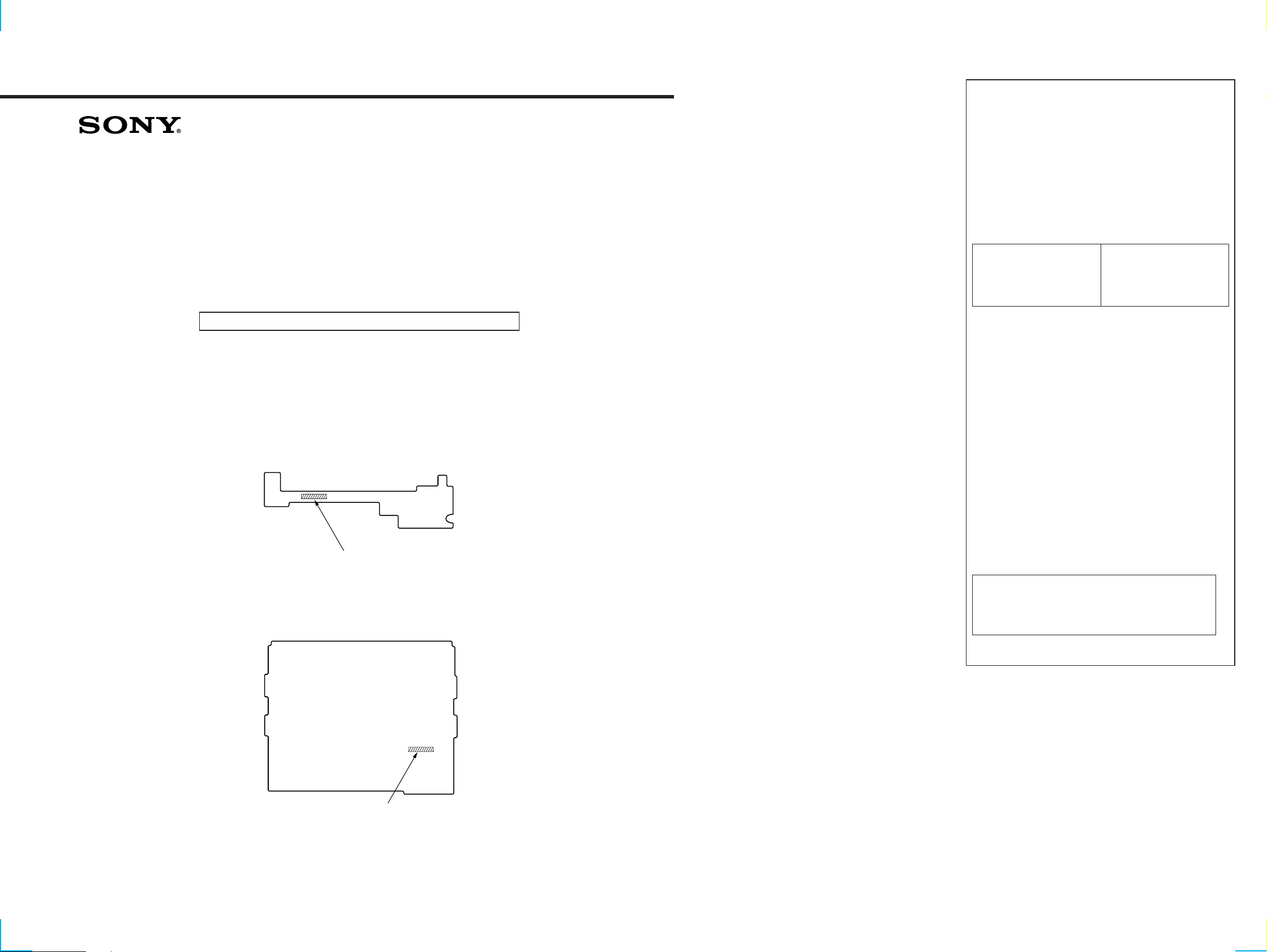
SUPPLEMENT-1
File this supplement with the service manual.
Subject : Change of Main and Relay Boards
(ECN-CSA00017)
When performing service and inspection, check the suffix of the part number of
the main and relay boards.
- RELAY BOARD - (SIDE A)
Relay board Part No.
Former : 1-672-698-11
New : 1-672-698-12
- MAIN BOARD - (SIDE A)
The components identified by
mark ! or dotted line with mark.
! are critical for safety.
Replace only with part number
specified.
• U : B+ Line.
• Power voltage is dc 14.4V and f ed with regulated dc power
supply from ACC and BATT cords.
• Voltages are tak en with a V OM (Input impedance 10 MΩ).
Voltage variations may be noted due to normal production tolerances.
• Waveforms are taken with a oscilloscope.
Voltage variations may be noted due to normal production tolerances.
• Circled numbers refer to waveforms.
• Signal path.
F : FM
f : AM
J : CD
• (( )) : Page of service manual.
<< >> : Page of supplement-1.
For printed wiring boards
• X : parts extracted from the component side.
• Y : parts extracted from the conductor side.
r
•
•
• b : Pattern from the side which enables seeing.
Caution:
Pattern face side: Parts on the pattern face side seen from the
(Side B) pattern face are indicated.
Parts face side: Parts on the parts face side seen from the
(Side A) parts face are indicated.
• (( )) : Page of service manual.
: Through hole.
¢
: internal component.
(The other layer’s patterns are not indicated.)
<< >> : Page of supplement-1.
Les composants identifiés par une
marque ! sont critiques pour la
sécurité.
Ne les remplacer que par une piéce
portant le numéro spécifié.
Main board Part No.
Former : 1-672-697-11
New : 1-672-697-12
– 2 –
Page 2
CDX-C7850
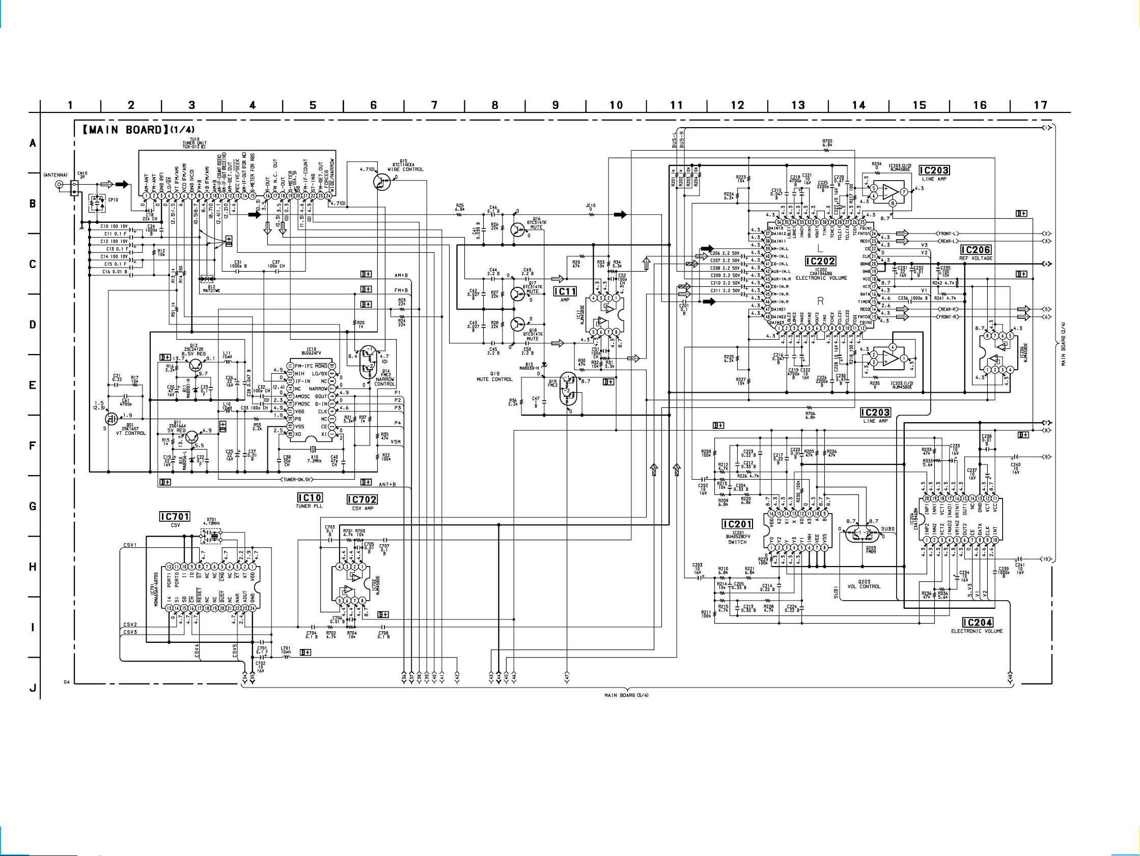
2. SCHEMATIC DIAGRAM — MAIN SECTION (1/4) —
((Page 9))
((Page 12))
– 7 – – 8 –
Note:
• Voltage is dc with respect to ground under
no-signal (detuned) condition.
no mark : FM
( ) : AM
Page 3

3. SCHEMATIC DIAGRAM — MAIN SECTION (2/4) —
((Page 8))
CDX-C7850
((Page 12))
((Page 13))
Note:
• Voltage is dc with respect to ground under
no-signal (detuned) condition.
no mark : FM
– 9 – – 10 –
Page 4

CDX-C7850
4. SCHEMATIC DIAGRAM — MAIN SECTION (3/4) —
((Page 8))
((Page 9))
((Page 13))
<<Page 42>>
Note:
• Voltage is dc with respect to ground under no-signal
(detuned) condition.
no mark : FM
(): AM
< > : CD PLAY
– 11 – – 12 –
Page 5

5. SCHEMATIC DIAGRAM — MAIN SECTION (4/4) —
CDX-C7850
((Page 9))
((Page 12))
((Page 17))
((Page 17))
Note:
• Voltage is dc with respect to ground under
no-signal (detuned) condition.
– 13 – – 14 –
no mark : FM
(): AM
< > : CD PLAY
Page 6

7. SCHEMATIC DIAGRAM — RELAY SECTION —
CDX-C7850
<<Page 61>>
((Page 14))
((Page 14))
– 17 –
 Loading...