

Page 1
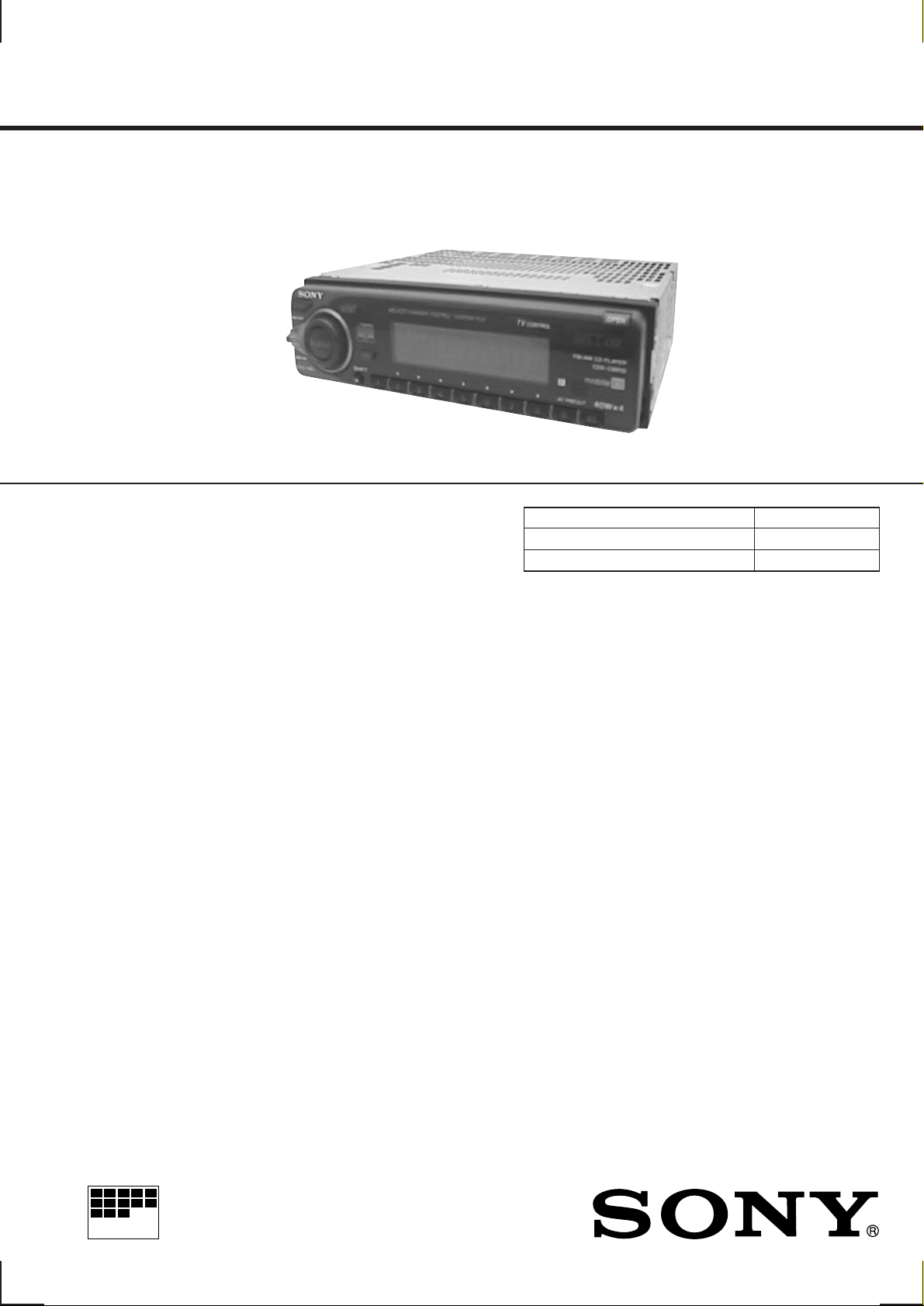
CDX-C6850
SERVICE MANUAL
SPECIFICATIONS
AUDIO POWER SPECIFICATIONS (US Model)
POWER OUTPUT AND TOTAL HARMONIC DISTORTION
17 watts per channel minimum continuous average power into
4 ohms, 4 channels driven from 20 Hz to 20 kHz with no more
than 1% total harmonic distortion.
US Model
Canadian Model
Model Name Using Similar Mechanism CDX-C5750/C5850
CD Drive Mechanism Type MG-363T-121
Optical Pick-up Name KSS-521A
Other Specifications
CD player section
System Compact disc digital audio
Signal-to-noise ratio 90 dB
Frequency response 10 – 20,000 Hz
Wow and flutter Below measurable limit
Laser Diode Properties
Material GaAlAs
Wavelength 780 nm
Emission Duration Continuous
Laser output power Less than 44.6 µW*
* This output is the value measured at a distance
of 200 mm from the objective lens surface on the
Optical Pick-up Block.
Tuner section
FM
Tuning range 87.5 – 107.9 MHz
Antenna terminal External antenna connector
Intermediate frequency 10.7 MHz
Usable sensitivity 10 dBf
Selectivity 75 dB at 400 kHz
Signal-to-noise ratio 65 dB (stereo),
Harmonic distortion at 1 kHz
Separation 35 dB at 1 kHz
Frequency response 30 – 15,000 Hz
AM
Tuning range 530 – 1,710 kHz
Antenna terminal External antenna connector
Intermediate frequency 10.71 MHz/450 kHz
Sensitivity 30 µV
system
68 dB (mono)
0.7% (stereo),
0.5% (mono)
Power amplifier section
Outputs Speaker outputs
(sure seal connectors)
Speaker impedance 4 – 8 ohms
Maximum power output 40 W × 4 (at 4 ohms)
General
Outputs Line outputs (2)
Power antenna relay
control lead
Power amplifier control
lead
Telephone ATT control
lead
Tone controls Bass ±8 dB at 100 Hz
Treble ±8 dB at 10 kHz
Power requirements 12 V DC car battery
(negative ground)
Dimensions Approx. 178 × 50 × 185 mm
(7 1/8 × 2 × 7 3/8 in.)
(w/h/d)
Mounting dimensions Approx. 182 × 53 × 162 mm
(7 1/4 × 2 1/8 × 6 1/2 in.)
(w/h/d)
Mass Approx. 1.2 kg (2 lb. 10 oz.)
Supplied accessories Parts for installation and
connections (1 set)
Front panel case (1)
Design and specifications are subject to change without
notice.
MICROFILM
FM/AM COMPACT DISC PLAYER
– 1 –
Page 2
SECTION 4
DIAGRAMS
4-1. IC PIN DESCRIPTION
• IC801 MB90574PFV-G-179-BND (SYSTEM CONTROL)
Pin No. Pin Name I/O Pin Description
1 LD ON O Laser ON/OFF control output
2 FOK I Focus OK signal detection input
3 XLAT25 O CD signal processing latch output
4 DATA25 O CD signal serial data output
5 XRST O Reset output to CD signal processor IC.
6 GFS I GFS signal detection input
7 NIL — Not used. (Connect to ground in this set.)
8 VCC — Power supply pin (+5 V)
9 – 11 NIL — Not used. (Open)
12 FLS SI/NOSE1 I Front panel attachment detection input
13 LCD SO/FLS SO O LCD serial data output
14 LCD CKO O LCD serial clock output
15 BEEP O BEEP output
16 NIL — Not used. (Open)
17 SQ SI I Sub Q data input
18 NIL — Not used. (Connect to ground in this set.)
19 SQ CKO O Sub Q read clock output
20 UNI SI I BUS system serial interface input
21 UNI SO O BUS system serial interface output
22 UNI CK I/O BUS system serial clock input/output
23 C IN I Track jump No. count input
24 SIRCS I Remote commander input
25 TXT SI I CD-TEXT data input
26 NIL — Not used. (Connect to ground in this set.)
27 TXT CKO O CD-TEXT data read clock output
28 CLOK25 O CD signal processing serial clock output
29 SYSRST O System reset output
30 DEEMPH O De-emphasis output
31 AMP ATT O Power amplifier attenuator control output
32 MD ON O CD mechanism power control output
33 VSS — Ground
34 C — Power stabilization capacitor pin
35 CD ON O CD power control output
36 BUS ON O BUS ON control output
37 AD ON O Power control output of A/D conversion.
38 DVCC — VREF input of D/A converter.
39 DVSS — Ground of D/A converter.
40 NIL — Not used. (Open)
41 ANGLE O LCD view angle alignment output (Not used in this set.)
42 AVCC — Analog power supply pin (+5 V)
43 AVRH — VREF + input of A/D converter.
44 AVRL — VREF – input of A/D converter.
45 AVSS — Analog ground
46 – 48 KEY IN0 – 2 I Key input 0 – 2
49 RC IN0 I Rotary commander input 0
50 QUALITY I Not used in this set.
51 NIL — Not used. (Connect to ground in this set.)
52 MPDH I Tuner multi path input (Not used in this set.)
53 S-METER I S-meter voltage detection input
54 VCC — Power supply pin (+5 V)
55 NS MASK O Not used in this set.
– 20 –
Page 3
Pin No. Pin Name I/O Pin Description
56 AMP ON O Power amplifier power control output
57 TXT ON O Reset output to CD-TEXT decoder IC.
58 VOL ATT O Electric volume mute control output
59 NIL — Not used. (Open)
60 ATT O System attenuate control output
61 RC IN1 I Rotary commander shift key input 1
62 TU ATT O Tuner attenuate output (Not used in this set.)
63 VSS — Ground
64 NIL — Not used. (Open)
65 SSTOP I IF counter result signal detection input of PLL.
66 TEST I Test mode initial setting detection input
67 DAVN I RDS IC data acquisition detection input (Fixed at “L” in this set.)
68 FM ON/AM ON O FM ON output
69 TU ON O Tuner power control output
70 SDA I/O I2C BUS serial data input/output
71 SCL O I2C BUS serial clock output
72 NOSE2 I Front panel OPEN detection input (Not used in this set.)
73 X1A O Sub ceramic oscillator output (32 kHz)
74 X0A I Sub ceramic oscillator input (32 kHz)
75 SCOR I SCOR signal detection input
76 BU IN I Backup power detection input
77 DQSY I CD-TEXT data setting completion signal detection input
78 CD SENS I CD SENS signal detection input
79 KEY ACK I Key input acknowledge
80 TEL ATT I Telephone attenuate detection input
81 ST/MONO I/O Tuner stereo signal detection input/forced monaural output
82 SEEKOUT O SEEK output
83 SD IN I Signal detector input
84 WIDE O WIDE/NARROW select output (Not used in this set.)
85 NARROW O WIDE/NARROW select output (Not used in this set.)
86 HSTX — Hardware standby input (Connect to pin (º (RESET).)
87 MD2 — Operation mode input (Connect to ground in this set.)
88, 89 MD1, 0 — Operation mode input (Connect to VCC in this set.)
90 RESET I Reset input
91 VSS — Ground
92 X0 I Main ceramic oscillator input (4.19 MHz)
93 X1 O Main ceramic oscillator output (4.19 MHz)
94 VCC — Power supply pin (+5 V)
95 COM8V ON O COM 8V control output
96 NIL — Not used. (Open)
97 AREA1 I Destination select input 1 (Fixed at “L” in this set.)
98 AREA2 I Destination select input 2 (Fixed at “L” in this set.)
99 AREA3 I Destination select input 3 (Fixed at “H” in this set.)
100 BAND I Not used in this set.
101 ACC IN I Accessory power detection input
102, 103 PH3, 2 I Disc insertion detection photo sensor input (Not used in this set.)
104 LCD CE O LCD chip enable output
105 FLS W I Flash write input (Fixed at “H” in this set.)
106, 107 RE IN0, 1 I Rotary encoder input
108 ILL ON O Illumination power control output
109 PW ON O System power control output
110 NIL — Not used. (Open)
111 ANT REM O ANT REMOTE power control output
– 21 –
Page 4

Pin No. Pin Name I/O Pin Description
112, 113 NIL — Not used. (Open)
114 CD LD O Loading motor control output (Loading direction)
115 CD EJ O Loading motor control output (Eject direction)
116 L SW I Sled limit switch detection input
117 IN SW/(PH1) I Disc insertion detection input
118 D SW I DOWN switch detection input
119 VSS — Ground
120 SELF SW/(IN SW) I Disc self store detection input
– 22 –
Page 5

4-6. SCHEMATIC DIAGRAM — CD MECHANISM SECTION — • Refer to page 28 for Waveforms.
• Refer to page 48 for IC Block Diagrams.
CDX-C6850
(Page 37)
– 31 – – 32 –
note:
• Voltage and waveforms are dc with respect to ground
under no-signal conditions.
no mark : CD PLAY
: Impossible to measure
∗
Page 6

CDX-C6850
4-8. SCHEMATIC DIAGRAM — MAIN SECTION (1/2) — • Refer to page 48 for IC Block Diagrams.
(Page 32)
(Page 39)
– 37 – – 38 –
note:
• Voltage is dc with respect to ground under no-signal
(detuned) condition.
no mark : FM
( ) : AM
< > : CD PLAY
Page 7

4-9. SCHEMATIC DIAGRAM — MAIN SECTION (2/2) — • Refer to page 50 for IC Block Diagrams.
CDX-C6850
(Page 38)
(Page 47)
– 39 – – 40 –
note:
• Voltage is dc with respect to ground under no-signal
(detuned) condition.
no mark : FM
( ) : AM
< > : CD PLAY
Page 8

4-11. SCHEMATIC DIAGRAM — DISPLAY SECTION —
(Page 47)
CDX-C6850
note:
• Voltage is dc with respect to ground under no-signal
– 43 – – 44 –
(detuned) condition.
no mark : FM
Page 9

4-13. SCHEMATIC DIAGRAM — RELAY SECTION —
CDX-C6850
(Page 43)
(Page 40)
– 47 –
Page 10

• IC Block Diagrams
REFERENCE
REFERENCE
VCCL
VCCL
VCCL
INL
SVRL
INML
INMR
SVRR
INR
VCCR
VCCR
VCCR
BUFFER
BUFFER
BUFFER
BUFFER
LIFT
AMP
SIGNAL
AMP
LIFT
AMP
SIGNAL
AMP
CL+
CL–
LGND
OUTL
OUTR
RGND
CR–
CR+
16
15
14
13
12
11
10
9
8
7
6
5
4
3
2
1
IC1 CXD2507AQ
1
FOK
2
MON
3
MDP
4
MDS
5
LOCK
TEST
6
7
FILO
8
FILI
9
PCO
10
VSS
11
AVSS
12
CLTV
AVDD
13
RF
14
BIAS
15
ASYI
16
ASYO
17
ASYE
18
WDCK
19
SERVO AUTO
SEQUENCER
INTERFACE
14
DIGITAL
PLL
ASYMMETRY
CORRECTOR
5
64
CPU
XLON
63
SPOD
62
SPOC
16K
RAM
VDD
CLKO
SPOB
SPOA
58596061
5
SUB CODE
PROCESSOR
EFM
DEMODULATOR
3
ERROR
CORRECTOR
XLTO
DATO
CNIN
5657
4
D/A
INTERFACE
3
IC402, 403 TDA8574
XLAT
CLOK
SEIN
52
5455
53
51
DATA
50
XRST
49
SENS
48
MUTE
47
SQCK
SQSO
46
45
EXCK
44
SBSO
43
SCOR
42
VSS
41
WFCK
40
EMPH
39
DOUT
C4M
38
37
FSTT
36
XTSL
35
XTAO
34
XTAI
MNTO
33
6
DIGITAL
CLV
DIGITAL
OUT
CLOCK
GENERATOR
20 21 22 23 24 25 26 27 293031 3228
GFS
GTOP
XUGF
XPCK
VDD
RFCK
C2PO
XROF
MNT3
MNT1
LRCK
PCMD
BCLK
IC3 BA6796FP-T1
OP IN –
OP IN +
VREF
CH3
CH3-IN
28
1
OPOUT
26
27
CTL1 CTL2 FWD REV
23 4
CH4
CH4-IN
THERMAL
SHUT
DOWN
CTL1
2425
LOGIC
5
CTL2
LEVEL
SHIFT
CH2
23
78
6
FWD
REV
22
CH2-IN
LEVEL
SHIFT
VCC
LEVEL
SHIFT
V/I
TRAY
– 48 –
VCC
21
DRIVE
BUFFER
9
10
GND
CH1
CH5 –
1920
CH1-IN
DRIVE
BUFFER
DRIVE
BUFFER
11
CH1 +
LEVEL
SHIFT
COM
CH1 –
DRIVE
BUFFER
DRIVE
BUFFER
12 13
CH4 +
161718
DRIVE
BUFFER
DRIVE
BUFFER
CH2 +
CH3 +
15
DRIVE
BUFFER
DRIVE
BUFFER
14
CH2 –
CH3 –
Page 11

IC2 CXA1782BQ
36 35 34
33
32
31
30 29 28 27 26 25
24
23
22
21
20
19
18
17
16
15
14
13
12
11
10
987
6
5
43
2
1
37
38
39
40
41
42
43
44
45
46
47
48
PHD 2
PHD 1
PHD
LD
RF O
RF I
CP
CB
CC1
CC2
FOK
SENS
C.OUT
XRST
DATA
XLT
CLK
VCC
ISET
SL O
SL M
SL P
TA O
TA M
FSET
TG2
TGU
SRCH
FE O
FLB
FGD
FDFCT
FE M
FEI
FEO
FE BIAS
F
E
EI
VEE
TED
LPFI
TEI
ATSC
TZC
TDFCT
VC
APC
LEVEL S
FOK
MIRR
RF IV AMP1
RF IV AMP2
FE AMP
TTL
IIL
FZC COMP
DFCT
IIL
TTL
IIL DATA REGISTER
INPUT SHIFT REGISTER
ADDRESS DECODER
OUTPUT DECODER
TTL
IIL
TOG1-3
BAL1-3
FS1-4 TG1-2 TM1-7 PS1-4
F IV AMP
E IV AMP
BAL1
BAL2
BAL 3
TE AMP
TZC COMP
DFCT
TM1
DFCT
FS4
ATSC
WINDOW COMP
TOG1
TOG2
TOG3
FCS PHASE
COMPENSATION
FS1
F SET
TG2
TM7
TM3
TM4
TM5
TM6
ISET
TRACKING
PHASE
COMPENSATION
HPF COMP
LPF COMP
TG1
FS2
TM2
RF M
– 49 –
Page 12

IC401 TDA7462D
PAUSE
DETECT
SE3L
28
SE3R
27
MUTE
26
SDA
25
SCL
24
PAUSE
23
SE1L
SE1R
MD+
MD–
CDL+
CDL–
CDR–
CDR+
PDR
PDGND
PDL
SE2L
SE2R
CREF
OUT
IIC
BUS
FRONT
FADER
FRONT
FADER
REAR
FADER
REAR
FADER
SDA
SCL
POWER
SUPPLY
22
21
20
19
18
17
16
15
OUT FL
OUT FR
OUT RL
OUT RR
SUBOUT+
SUBOUT–
VDD
GND
INPUT
SELECTOR
FRONT SIDE
SELECTOR
REAR SIDE
GAIN &
AUTO
ZERO
INPUT
GAIN
BEEP
1
2
3
4
5
6
7
8
9
10
11
12
13
14
MIXING STAGE
INPUT MULTIPLEXER &
LOUDNESS
CONTROL
CIRCUIT
LOUDNESS
CONTROL
CIRCUIT
VOLUME
CONTROL
CIRCUIT
COMPANDER
DIGITAL CONTROL CIRCUIT
SOFT
MUTE
TREBLE/
BASS
CONTROL
CIRCUIT
VOICE BANDPASS
HP LP
SUBWOOFER
LP
FADER
SUBWOOFER
IC702 PCM1717E-S
1
XTI
2
DGND
3
VDD
4
LRCIN
5
DIN
BCKIN
6
7
ZERO
D/C R
8
9
VOUTR
10
AGND
INPUT
INTERFACE
DIGITAL
FILTER
NOISE SHAPER
5LEVE DAC
LOWPASS FILTER
CMOS
AMP
CLK
CONTROL
LOWPASS FILTER
MODE
CONT
ROL
5LEVEL DAC
CMOS
AMP
20
19
18
17
16
15
14
13
12
11
XTO
CLKO
ML/MUTE
MC/DM1
MD/DM0
RSTB
MODE
D/C L
VOUTL
VCC
IC901 BA4903
5.7V
ON ON
AMPONAMP
+–
OUT
THERMAL
SHUT
DOWN
CIRCUIT ON
GND VCC VDD
+–
REGULATOR
VREF
OVER
VOLTAGE
PROTECT
51 2 3 4
OUT
– 50 –
Page 13

IC601 TDA7427AD1
LP FM
1
LP HC
2
LP AM
3
V REF
4
LCL/DX
5
SEEK
6
NIL
7
MONO
8
SWITCH
LP1/LP2
PORT
EXTENSION
TEST
LOGIC
CHARGE
PUMP
PHASE
COMP
INLOCK
DETECTOR
11 BIT PROG
COUNTER
SWITCH
SWM/DIR
6 BIT PROG
COUNTER
SWITCH
SWM/DIR
PRE COUNTER
:32/33
SWITCH
AM/FM
VDD1
28
27
26
25
24
23
LPOUT
VDD2
GND AM
AM IN
FM IN
NC
OSCIN
9
OSCOUT
10
NC
11
SCL
12
SDA
IF AM
INTERFACE
13
14
IC703 LC89170M-T
EXCK
1
2
SBSO
3
SCOR
I2C BUS
REF
OSCILLATOR
14 BIT PROG
COUNTER
SWITCH
AM/FM
32 WORD X 8 BIT
DUAL PORT RAM
16 BIT PROG
COUNTER
TIMER CONTROL
11-21 BIT PROG COUNTER
CPU INTERFACE
CHECKER
CRC
VDD
POWER ON
SWITCH
OUT
SUPPLY
&
RESET
22
GND D
21
VDD1
20
ADDR
19
HFREF
AMOSC
18
DOUT/INLOCK
17
SSTOP
16
15
IF FM
IC803 BA8270F-E2
BUS ON
1
14
VDD
2
13
DQSY
SRDT
12
RST
BATT
3
BUS ON
SWITCH
RESET
SWITCH
BATTERY
SWITCH
14
13
12
11
10
VCC
RST
BUS ON
CLK IN
BU IN
WFCK
MCK
XMODE
GND
4
5
6
7
TIMING
&
SYNCHRONIZATION
SIGNAL
PROTECTION
11
SCLK
10
SW2
SW1
9
8
TEST
4
CLK
5
VREF
6
DATA
GND
7 8
DATA IN
9
DATA OUT
– 51 –
 Loading...