

Page 1
CD-SW200E
In the interests of user-safety the set should be restored to its
original condition and only parts identical to those specified be
used.
SERVICE MANUAL
No. XXXXXXXXXXXXX
MINI COMPONENT SYSTEM
CONTENTS
CHAPTER 1. GENERAL DESCRIPTION
[1] Specifications ................................................. 1-1
[2] Names of parts............................................... 1-2
CHAPTER 2. ADJUSTMENTS
[1] Mechanism section ........................................ 2-1
[2] Tuner section ................................................. 2-1
[3] TEST MODE .................................................. 2-2
[4] CD SECTION ................................................. 2-4
[5] CD section...................................................... 2-4
[6] Standard Specification of Stereo System
Error Message Display Contents ................... 2-4
[7] CD Changer mechanism section ................... 2-5
MODEL
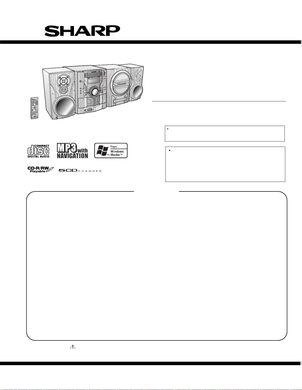
CD-SW200E Mini Component System consisting of CD-SW200E
(main unit) CP-S200H (front speaker) and CP-SW200E (subwoofer).
Note for users in U.K.
Recording and playback of any material may require consent
which SHARP is unable to give. Please refer particularly to the
provisions of Copyright Act 1956, the Dramatic and Musical
Performers Protection Act 1956, the Performers Protection Acts
1963 and 1972 and to any subsequent statutory enactments and
orders.
CHAPTER 5. CIRCUIT DESCRIPTION
[1] Notes on schematic diagram .........................5-1
[2] Types of transistor and LED ..........................5-1
[3] Waveforms of CD circuit................................5-2
[4] Voltage...........................................................5-3
CHAPTER 6. CIRCUIT SCHEMATICS AND PARTS
LAYOUT
[1] Schematic diagram........................................6-1
[2] Wiring side of PWB...................................... 6-11
CHAPTER 7. FLOWCHART
[1] Troubleshooting.............................................7-1
CD-SW200E
CHAPTER 3. MECHANISM BLOCKS
[1] Caution on diassembly................................... 3-1
[2] Removing and reinstalling the main parts ........ 3-4
CHAPTER 4. DIAGRAMS
[1] Block diagrams............................................... 4-1
Parts marked with " " are important for maintaining the safety of the set. Be sure to replace these parts with specified ones for
maintaining the safety and performance of the set.
SHARP CORPORATION
CHAPTER 8. OTHERS
[1] Function table of IC .......................................8-1
[2] FL Display......................................................8-9
Parts Guide
This document has been published to be used
for after sales service only.
The contents are subject to change without notice.
Page 2
CD-SW200E
SAFETY PRECAUTION FOR SERVICE MANUAL
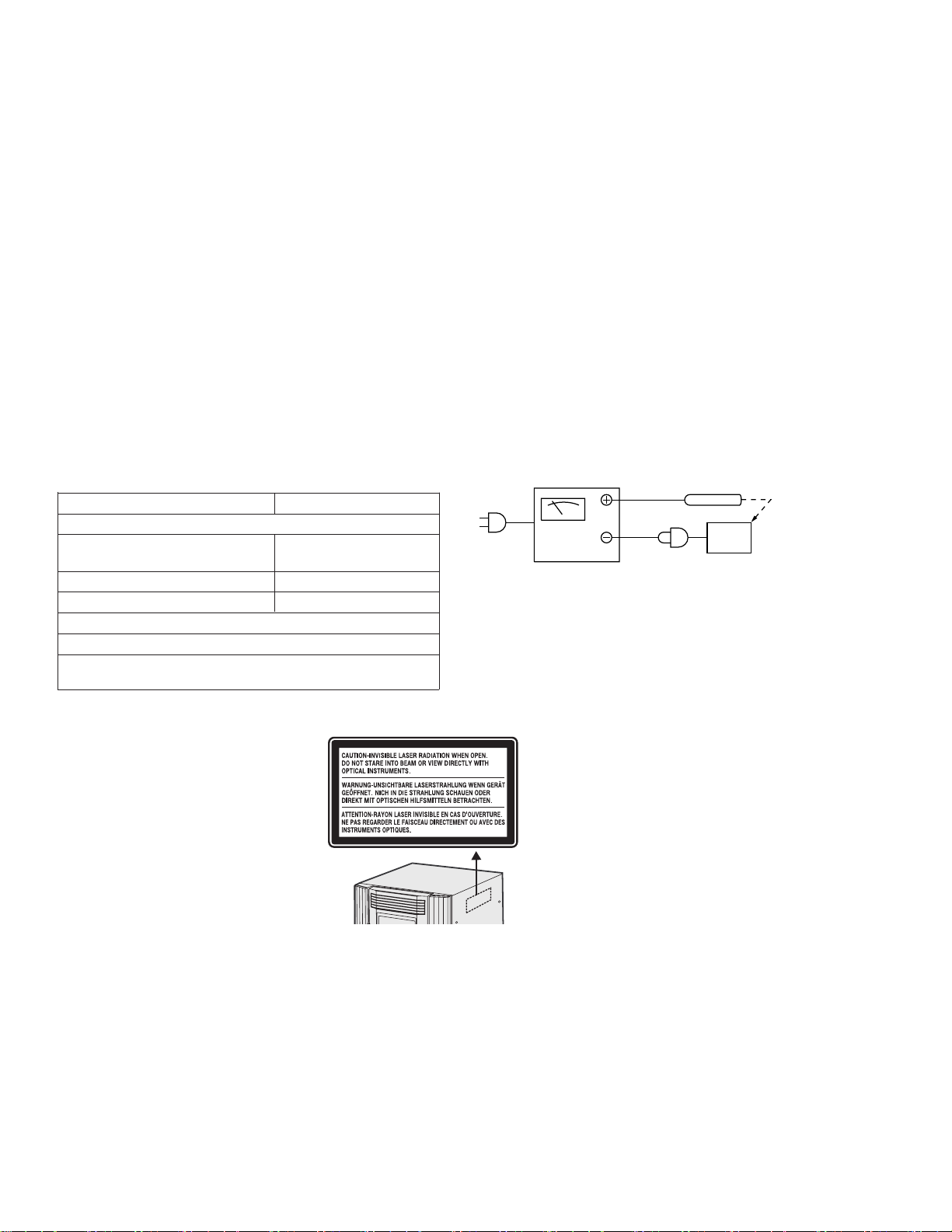
Precaution to be taken when replacing and servicing the Laser Pickup.
The AEL (Accessible Emission Level) of Laser Power Output for this model is specified to be lower than Class 1 Requirements.
However, the following precautions must be observed during servicing to protect your eyes against exposure to the Laser beam.
(1) When the cabinet has been removed, the power is turned on without a compact disc, and the Pickup is on a position outer than
the lead-in position, the Laser will light for several seconds to detect a disc. Do not look into the Pickup Lens.
(2) The Laser Power Output of the Pickup inside the unit andreplacement serviceparts have already been adjusted prior to shipping.
(3) No adjustment to the Laser Power should be attempted when replacing or servicing the Pickup.
(4) Under no circumstances look directly into the Pickup Lens at any time.
(5) CAUTION - Use of controls or adjustments, or performance of procedures other than those specified herein may result in
hazardous radiation exposure.
IMPORTANT SERVICE NOTES (FOR U.K. ONLY)
Before returning the unit to the customer after completion of a
repair or adjustment it is necessary for the following withstand
voltage test to be applied to ensure the unit is safe for the
customer to use.
Setting of Withstanding Voltage Tester and set.
Set name set value
Withstanding Voltage Tester
Test voltage 4,240 VPEAK
3,000 VRMS
Set time 6 secs
Set current (Cutoff current) 4 mA
Unit
Judgment
OK: The "GOOD" lamp lights.
NG: The "NG" lamp lights and the buzzer sounds.
WITHSTANDING
VOLTAGE TESTER
AC
OUT
SHORT-CIRCUIT
AC POWER
SUPPLY CORD
PROBE
UNIT
CONNECT THE PROBE
TO GND OF CHASSIS
SCREW
Laser Diode Properties
Material: GaAIAs
Wavelength: 795 nm
Emission Duration: continuous
Laser Output: max. 0.6 mW
– i –
Page 3
CD-SW200E
1. Employing lead-free solder
"Main/Display/Tumer/Power/Game Input/CD Servo PWB/LED" of this model employs lead-free solder. The LF symbol indicates
lead-free solder, and is attached on the PWB andservice manuals. The alphabetical character following LF shows the type of
lead-free solder.
Example:
Indicates lead-free solder of tin, silver and copper.
2. Using lead-free wire solder
When fixingthe PWBsoldered withthe lead-free solder, apply lead-free wire solder. Repairing with conventional lead wire solder
may cause damage or accident due to cracks.
As the melting point of lead-free solder (Sn-Ag-Cu) is higher than the lead wire solder by 40 C, we recommend you to use a
dedicated soldering bit, if you are not familiar with how to obtain lead-free wire solder or soldering bit, contact our service station
or service branch in your area.
3. Soldering
As the melting point of lead-free solder (Sn-Ag-Cu) is about 220 C which is higher than the conventional lead solder by 40 C,
and as it has poor solder wettability, you may be apt to keep the soldering bit in contact with the PWB for extended period of
time. However, Since the land may be peeled off or the maximum heat-resistance temperature of parts may be exceeded,
remove the bit from the PWB as soon as you confirm the steady soldering condition.
Lead-free solder contains more tin, and the end of the soldering bit may be easily corrected. Make sure to turn on and off the
power of the bit as required.
If a different type of solder stays on the tip of the soldering bit, it is alloyed with lead-free solder. Clean the bit after every use
of it.
When the tip of the soldering bit is blackened during use, file it with steel wool or fine sandpaper.
Be careful when replacing parts with polarity indication on the PWB silk.
Lead-free wire solder for servicing
Ref No. DescriptionParts No.
PWB-A 92LPWB6383MANS Main/Display
PWB-B 92LPWB6383PWRS Power/Game Input
PWB-C 92LPWB6230CDUS CD Servo
PWB-D 92LPWB6291TUNS Tuner
PWB-E 92LPWB6230LEDS LED
Page 4
CD-SW200E
AudioCD-SW200EService ManualCD-SW200EMarketE
CHAPTER 1. GENERAL DESCRIPTION
[1] Specifications
FOR A COMPLETE DESCRIPTION OF THE OPERATION OF THIS UNIT, PLEASE REFER
TO THE OPERATION MANUAL.
CD-SW200E
General
Power source AC 230 - 240 V, 50 Hz
Power consumption
Dimensions Width: 260 mm (10-1/4")
Weight 10.4 kg (22.9 lbs.)
200 W
Height: 330 mm (13")
Depth: 326 mm (12-7/8")
Amplifier
Output power Front Speaker:
Output terminals Front Speakers: 6 ohms
Input terminals Game/ Auxiliary (audio signal):
RMS: 200 W (100 W + 100 W) (10% T.H.D)
RMS: 156 W (78W+78W)(0.9% T.H.D)
Subwoofer:
RMS: 200 W (10% T.H.D)
RMS: 166 W (0.9% T.H.D)
Subwoofer: 12 ohms
Headphones: 16 - 50 ohms
(recommended: 32 ohms)
Video output: 1Vp-p
500 mV/ 47 k ohms
Game/Video: 1Vp-p
CD player
Type 5-disc multi-play compact disc player
Signal readout Non-contact, 3-beam semiconductor laser
D/A converter 1-bit D/A converter
Frequency
response
Dynamic range 90 dB (1 kHz)
pickup
20 - 20,000 Hz
Tuner
Frequency range FM: 87.5 - 108.0 MHz
AM: 522 - 1,620 kHz
Cassette deck
Frequency
response
Signal/noise ratio 55 dB (TAPE 1, playback)
Wow and flutter 0.3 % (WRMS)
50 - 14,000 Hz (normal tape)
50 dB (TAPE 2, recording/playback)
CP-S200H
Type 3-way type speaker system
Super tweeter
5 cm (2") tweeter
13 cm (5-1/8") woofer
Maximum input
power
Rated input power 100 W
Impedance 6 ohms
Dimensions Width: 180 mm (7-1/16")
Weight 3.0 kg (6.6 lbs.) /each
200 W
Height: 330 mm (13")
Depth: 212 mm (8-6/16")
CP-SW200E
Type Full Range
20 cm (8") subwoofer
Maximum input
power
Rated input power 200 W
Impedance 12 ohms
Dimensions Width: 250 mm (9-13/16")
Weight 5.9 kg (13 lbs.)
400 W
Height: 330 mm (13")
Depth: 294 mm (11-9/16")
Specifications for this model are subject to change without
prior notice.
1 – 1
Page 5
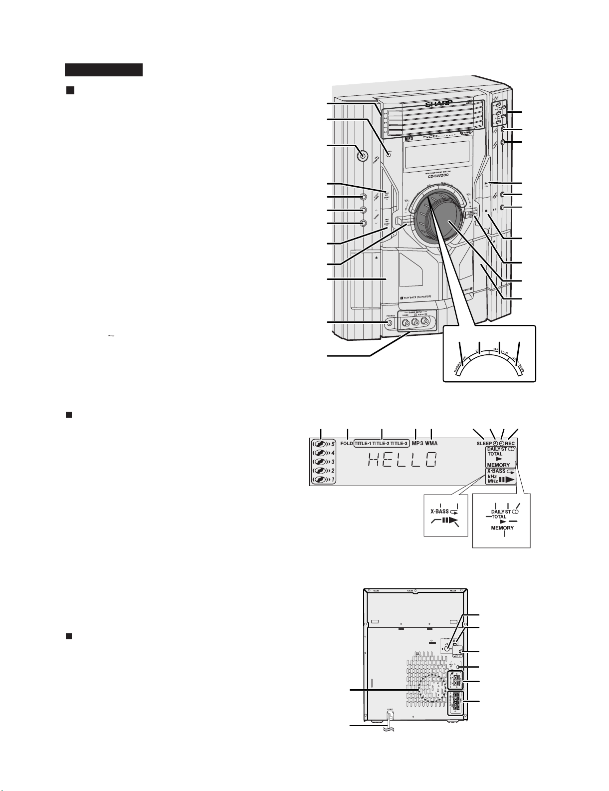
[2] Names of parts
CD-SW200E
Front panel
1. Disc Trays
2. Timer Indicator
3. On/Stand-by Button
4. Disc Track Up or Fast Forward, Tape 2 Fast Forward,
Tuner Preset Up, Time Up Button
5. Clock/Timer Button
6. Tuning Up Button
7. Tuning Down Button
8. Disc Track Down or Fast Reverse, Tape 2 Rewind,
Tuner Preset Down, Time Down Button
9. Equalizer Mode Select Button
10. Tape 1 Cassette Compartment
11. Headphone Socket
12. Game/Video Input Socket
13. Disc Number Select Buttons
14. Disc Direct Play Button
15. Disc Tray Open/Close Button
16. Disc Play or Repeat, Tape Play Button
17. Memory/Set Button
18. Tape 2 Record Pause Button
19. Disc or Tape Stop Button
20. Extra Bass (Surround)/Demo Mode Button
21. Volume Control
22. Tape 2 Cassette Compartment
23. Tuner (Band) Button
24. CD Button
25. Tape (1 2) Button
26. Game/Video Button
10
11
12
CD-SW200E
1
2
13
14
3
4
5
6
15
16
17
18
7
8
9
19
20
21
22
24 25 2623
Display
1. Disc Number Indicators
2. MP3/WMA Folder Indicator
3. MP3/WMA Title Indicators
4. MP3 Indicator
5. WMA Indicator
6. Sleep Indicator
7. Timer Play Indicator
8. Timer Recording Indicator
9. Tape 2 Record Indicator
10. MP3/WMA Total Indicator
11. Daily Timer Indicator
12. FM Stereo Mode Indicator
13. FM Stereo Receiving Indicator
14. Tape Play Indicator
15. Memory Indicator
16. Extra Bass Indicator
17. Disc Repeat Play Indicator
18. Disc Pause Indicator
19. Disc Play Indicator
Rear panel
1. Cooling Fan
2. AC Power Lead
3. FM 75 Ohms Aerial Terminal
4. AM Loop Aerial Socket
5. Subwoofer Light-up Socket
6. Video Output Socket
7. Subwoofer Terminals
8. Front Speaker Terminals
12 3 45 6789
10
11 12 13
14
16 17
18
19
15
3
4
5
6
7
1
8
2
1 – 2
Page 6
CD-SW200E
CD-SW200E
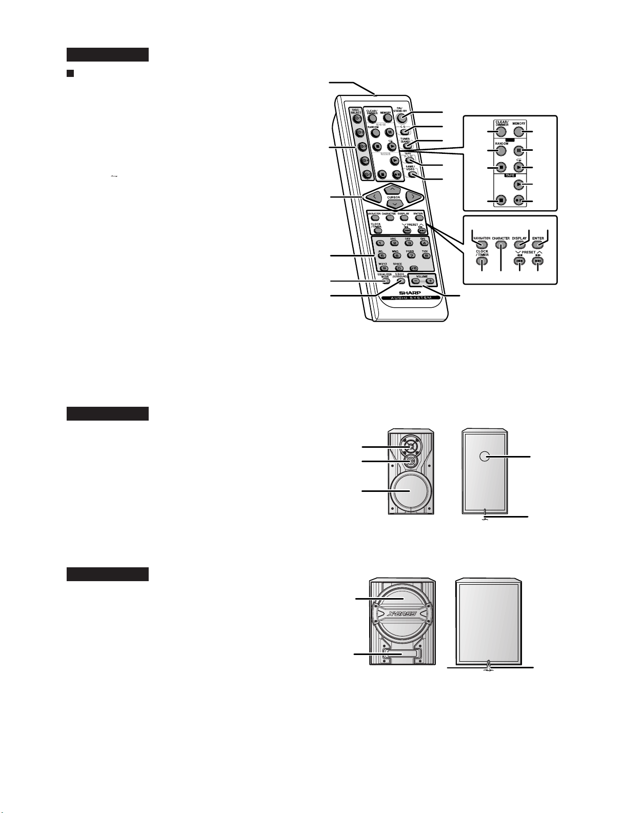
Remote control
1. Remote Control Transmitter
2. Disc Number Select Buttons
3. Cursor Buttons
4. Character Input/Disc Direct Search Buttons
5. Equalizer Mode Select Button
6. Extra Bass (Surround) Button
7. On/Stand-by Button
8. CD Button
9. Tuner (Band) Button
10. Tape (1 2) Button
11. Game/Video Button
12. Volume Up and Down Buttons
13. Disc Clear/Dimmer Button
14. Disc Random Button
15. Disc Stop Button
16. Tape Stop Button
17. Memory Button
18. Disc Pause Button
19. Disc Play or Repeat Button
20. Tape Play Button
21. Tape 2 Record Pause Button
22. MP3/WMA Navigation Mode Select Button
23. MP3/WMA Display Button
24. Enter Button
25. Clock/Timer Button
26. Character Button
27. Disc Track Down or Fast Reverse, Tape 2 Rewind,
Tuner Preset Down, Time Down Button
28. Disc Track Up or Fast Forward, Tape 2 Fast Forward,
Tuner Preset Up, Time Up Button
1
7
8
13
2
9
10
14
15
11
3
16
22
CD
17
18
19
20
21
23 24
4
5
6
25 26 27 28
12
CP-S200H
1. Tweeter
2. Super Tweeter
3. Woofer
4. Bass Reflex Duct
5. Speaker Wire
CP-SW200E
1. Subwoofer
2. Bass Reflex Duct
3. Subwoofer Light-Up Wire
4. Speaker Wire
1
2
4
3
5
11
2
3
4
1 – 3
Page 7
AudioCD-SW200EService ManualCD-SW200EMarketE
CHAPTER 2. ADJUSTMENTS
[1] Mechanism section
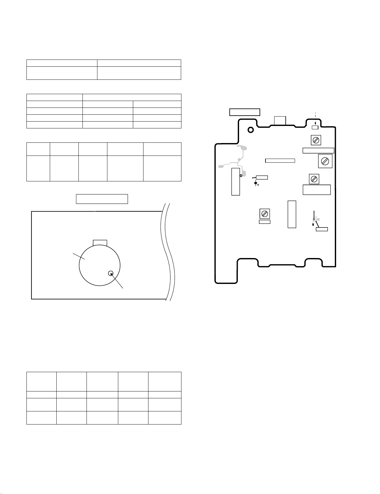
• Driving Force Check
Torque Meter Specified Value
Play: TW-2111 Tape 1: Over 80 g
Tape 2: Over 80 g
• Torque Check
CD-SW200E
•FM IF
Notes:
1. Description of the "FM IF Adjustment" is not carried on this Manual. It is because the IF coil in the FM front end section has been
best adjusted in the factory so that its further adjustment is not
needed at the field. When replacing the FM front end assembly, no
adjustment is needed either.
2. The parts in the FM front end section are prepared in a complete
unit, so you can't obtain each part individually.
Torque Meter Specified Value
Tape 1 Tape 2
Play: TW-2111 30 to 80 g.cm 30 to 80 g.cm
Fast forward: TW-2231 — 70 to 180 g.cm
— 70 to 180 g.cm
• Tape Speed
Normal
speed
Test Tape Adjust-
ing Point
MT T-111 Var iabl e
Resistor in
motor.
Specified
Val ue
3,000 ± 30 Hz
Speaker
Instrument
Connection
Speaker Terminal (Load
resistance: 6
ohms)
TAPE MECHANISM
Tape
Motor
TUNER PWB-D
20
IC302
TP301
C393
T351
AM IF
SO301
FM ANTENNA
TERMINAL
FE301
L341
AM TRACKING fL
T306
AM BAND
COVERAGE fL
IC303
AM
LOOP
ANTENNA
CNP302
R356
TP302
T303
Variable Resistor in motor
Figure 1
[2] Tuner section
fL: Low-range frequency
fH: High-range frequency
• AM IF/RF
Signal generator: 400 Hz, 30%, AM modulated
Test Stage Frequency Frequency
Display
AM IF 450 kHz 1,620 kHz T351 *1
AM Band
— 522 kHz (fL): T306
Coverage
AM
990 kHz 990 kHz (fL): T303 *1
Tracking
*1. Input: Antenna Output: TP302
*2. Input: Antenna Output: TP301
Setting/
Adjusting
Parts
1.1 ± 0.1 V
Figure 2 Adjustment Points
Instrument
Connection
*2
2 – 1
Page 8
CD-SW200E
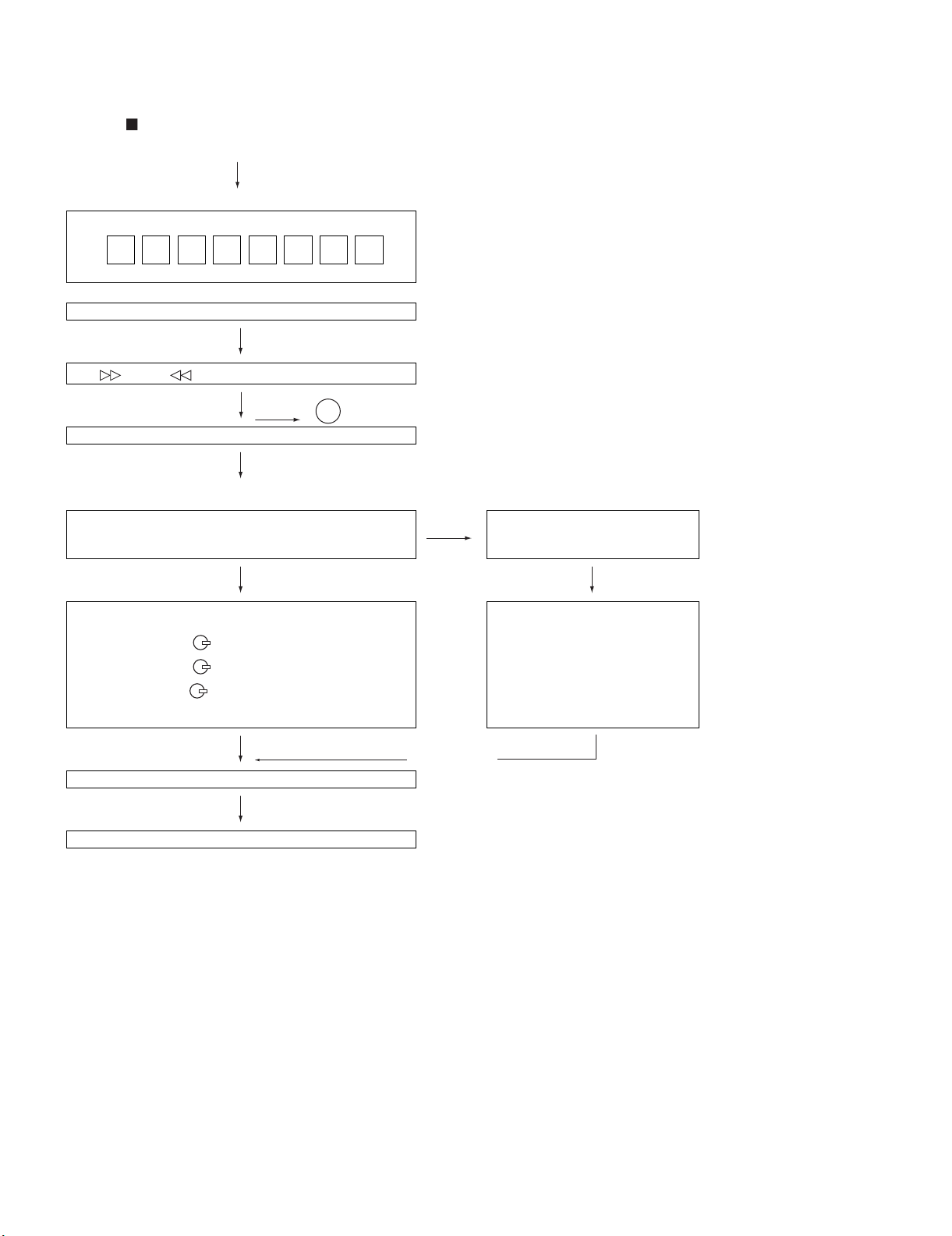
[3] TEST MODE
• Setting the test mode
During stand-by mode, press ON/STAND-BY button while pressing
down the button and X-BASS/DEMO button. then, press the CD
button to enter the test mode.
C D T E S T
OPEN/CLOSE operation is using manual. IL isn’t done
<< >>,<< >>buttons make pick's slide possible.
to page 2-3
<<PLAY>> key input.
Do TOC IL. Do normal play.
When these following key is input into PLAY key, track number can be appoint directly.
<< 1 >> key: Track 4
<< 2 >> key: Track 9
<< 3 >> key: Track 15
A
IL isn’t done
IL isn’t done
<<MEMORY>>
key input.
Adjustment result automatically will
display as below for each 2 sec:
a) “FOF_XXXX”
b) “TOF_XXXX”
c) “TBAL_XX”
d) “TGAN_XX”
f) “FGAN_XX”
g) “RFLS_XX”
<<STOP>> key input.
STOP
explanation:
a) Focus off set = “FOF_XXXX”
b)Tracking off set = “TOF_XXXX”
c)Tracking balance = “TBAL_XX”
d)Tracking Gain = “TGAN_XX”
f) Focus Gain = “FGAN_XX”
g) RF level shift = “RFLS_XX”
VOL — Last memory
P. G E Q — FL A T
X-BASS — OFF
To cancel: Power OFF
––––––––
2 – 2
Page 9
A
<<MEMORY>> key input.
Laser ON.
<<MEMORY>> key input.
Tracking OFF play at that specific point.
<<MEMORY>> key input.
Tracking ON play from that specific point.
CD-SW200E
<<MEMORY>> key input.
Adjustment result automatically will display as below for each 2 sec:
a) “FOF_XXXX”
b) “TOF_XXXX”
c) “TBAL_XX”
d) “TGAN_XX”
f) “FGAN_XX”
g) “RFLS_XX”
<<STOP>> key input.
STOP
Sliding the PICKUP with<< >>, << >> button must only be
in STOP mode.
explanation:
a) Focus off set = “FOF_XXXX”
b)Tracking off set = “TOF_XXXX”
c)Tracking balance = “TBAL_XX”
d)Tracking Gain = “TGAN_XX”
f) Focus Gain = “FGAN_XX”
g) RF level shift = “RFLS_XX”
VOL — Last memory
P. G E Q — FL A T
X-BASS — OFF
To cancel: Power OFF
2 – 3
Page 10
CD-SW200E
[4] CD SECTION
• Adjustment
Since this CD system incorporates the following automatic adjustment functions, readjustment is not needed when replacing the
pickup. Therefore, different PWBs and pickups can be combined
freely.
Each time a disc is changed, these adjustments are performed
automatically. Therefore, playback of each disc can be performed
under optimum conditions.
Items adjusted automatically
1) Offset adjustment (The offset voltage between the head amplifier
output and the VREF reference voltage is compensated inside the
IC.)
* Focus offset adjustment
* Tracking offset adjustment
2) Tracking balance adjustment
3) Gain adjustment (The gain is compensated inside the IC so that the
loop gain at the gain crossover frequency will be 0 dB.)
* Focus gain adjustment
* Tracking gain adjustment
[5] CD section
CD Error code description
Error Explanation
01 When Pickup set inner position, inner switch cannot detect
'ON' level for 10 secs.
10* CAM error. Can't detect CAM switch when CAM is moving.
11* When it detect cam operation error during initialize pro-
cess.
20* TRAY error. Can't detect TRAY switch when TRAY is mov-
ing.
21* When it detect TRAY operation error during initialize pro-
cess.
31 When it change to CD function, DSP cannot read initial
data.
* 'CHECKING'
If Error is detected, 'CHECKING' will be displayed instead of 'ERCD**'. 'ER-CD**' display will only be displayed when error had been
detected for the 5th times.
[6] Standard Specification of Stereo System Error Message Display Contents
Error Contents Display Notes
CD Pickup Mechanism Error. 'ER-CD01' PU-IN SW Detection NG.
CD Changer Mechanism Error. 'ER-CD**' (*) 10: CAM SW Detection NG during normal operation
11: CAM SW Detection NG during initialize process
20:TRAY SW Detection NG during normal operation
21:TRAY SW Detection NG during initialize process
CD DSP Communication Error. 'ER-CD31' DSP COMMUNICATION ERROR.
Focus Not Match/IL Time Over. 'NO DISC'
TUNER PLL Unlock. PLL Unlock.
(*) CHECKING:
If CD changer mechanism error is detected, ‘CHECKING’ will be display instead of ‘ER-CD**’. ‘ER-CD**’ display will only be display when
error had been detected for the 5 th times.
Speaker abnormal detection and +B PROTECTION display
In case speaker abnormal detection or +B PROTECTION had
occurred, the unit will automatically enter to stand-by mode and Timer
indicator will Flashing as below.
+B PROTECTION is condition when irregular process occur on power
supply line.
FM 87.5 MHz
BEFORE TRANSPORTING THE UNIT
The following process need to be taken after set tapering/parts
replacement.
1. Press the ON/STAND-BY button to enter stand-by mode.
2. While pressing down the button and the X-BASS/DEMO button, press the ON/STAND-BY button. The Micro Computer version
number will be displayed as “CN******”.
3. Press OPEN/CLOSE button until “WAIT”→ “FINISHED” appears.
4. Unplug the AC cord and the unit is ready for transporting.
Example: In case of speaker abnormal
ON FLASHING
TIMER
LED
OFF OFF OFF OFF
NO. 1
1 FRAME
NO.1:+BPROTECTION
NO. 2 : Speaker abnormal
NO. 2
FLASHINGON
NO. 1
NO. 2
(REPEAT)
2 – 4
Page 11
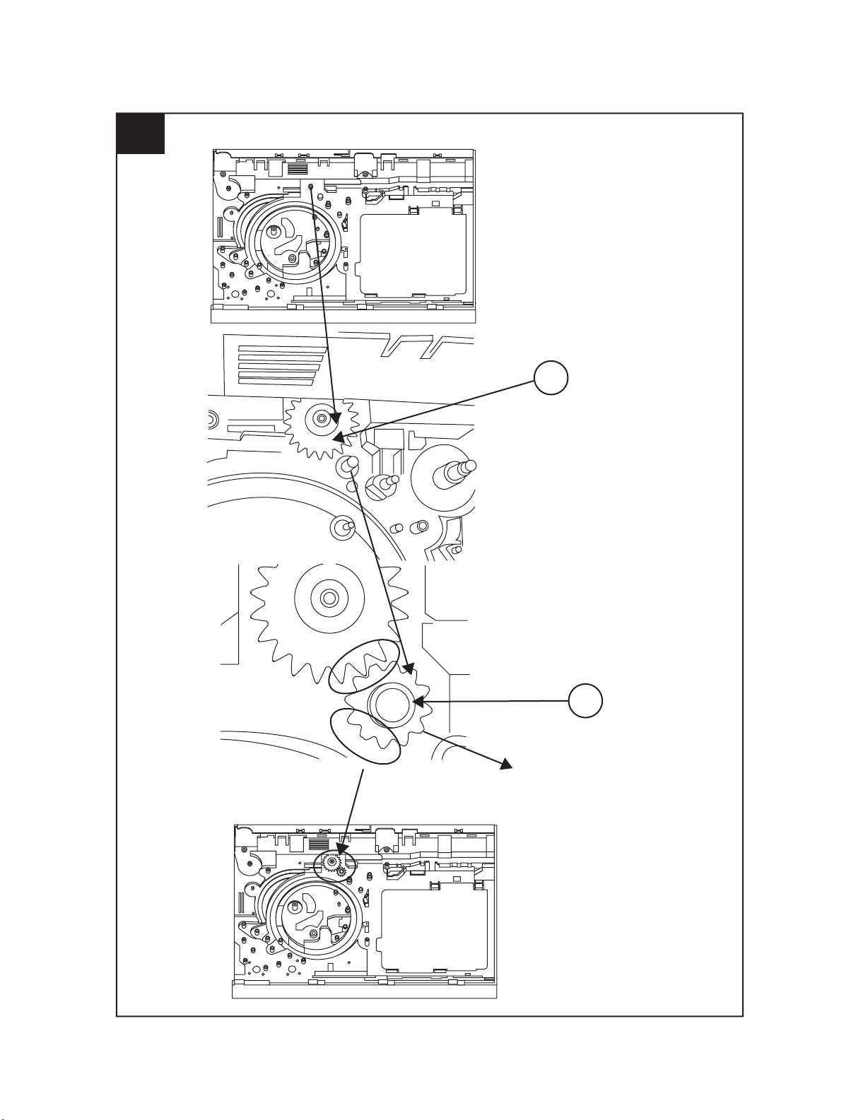
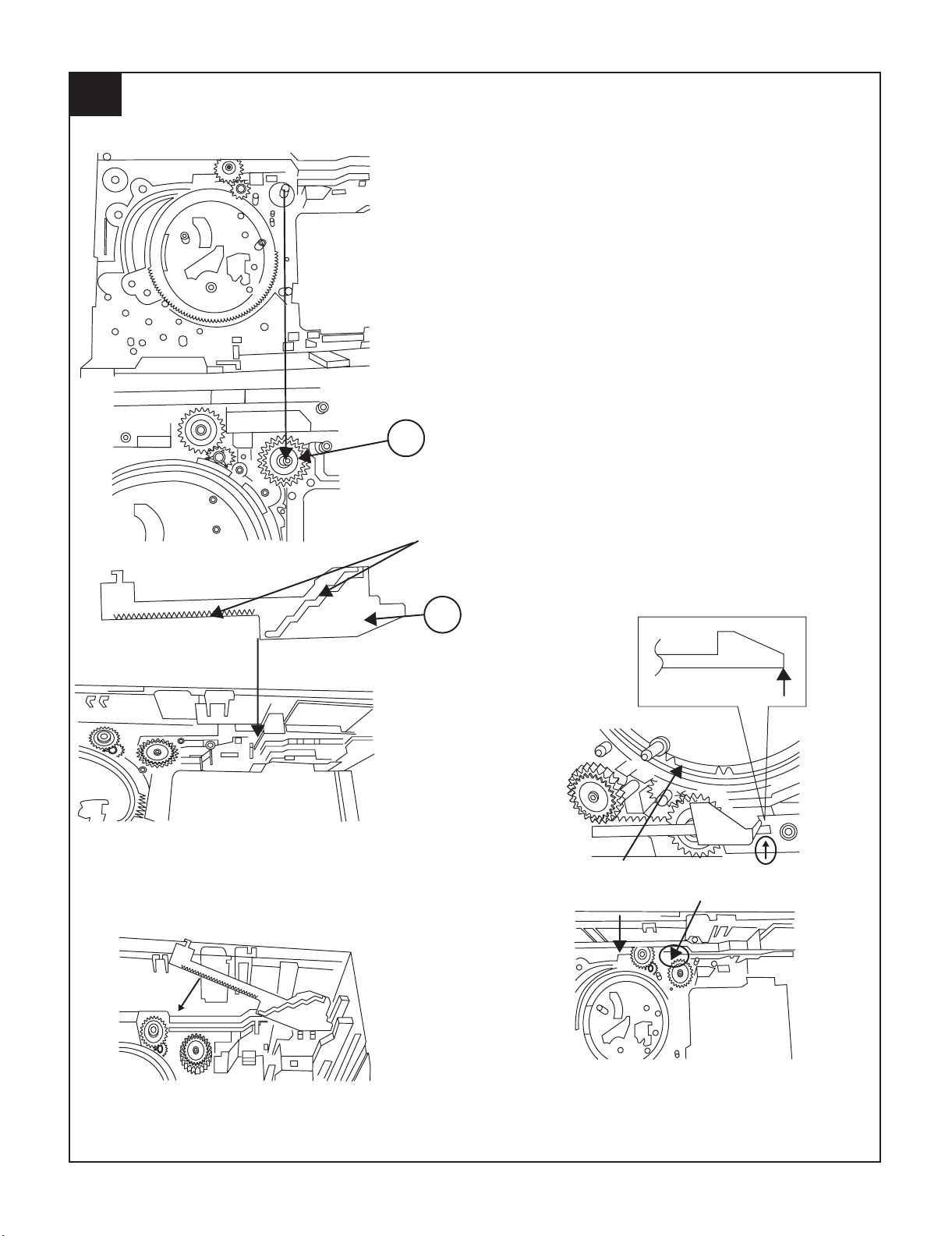
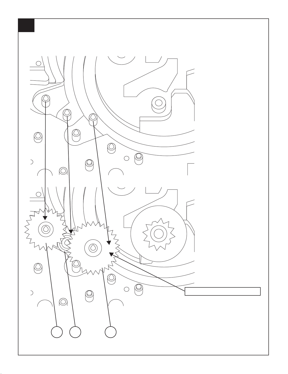
[7] CD Changer mechanism section
• A number in the drawing sheet is the number of the parts guide
(CHANGER MECHANISM PARTS).
1
CD-SW200E
141
2 – 5
140
HALF GEAR
MUST ARRANGE AS SHOWN
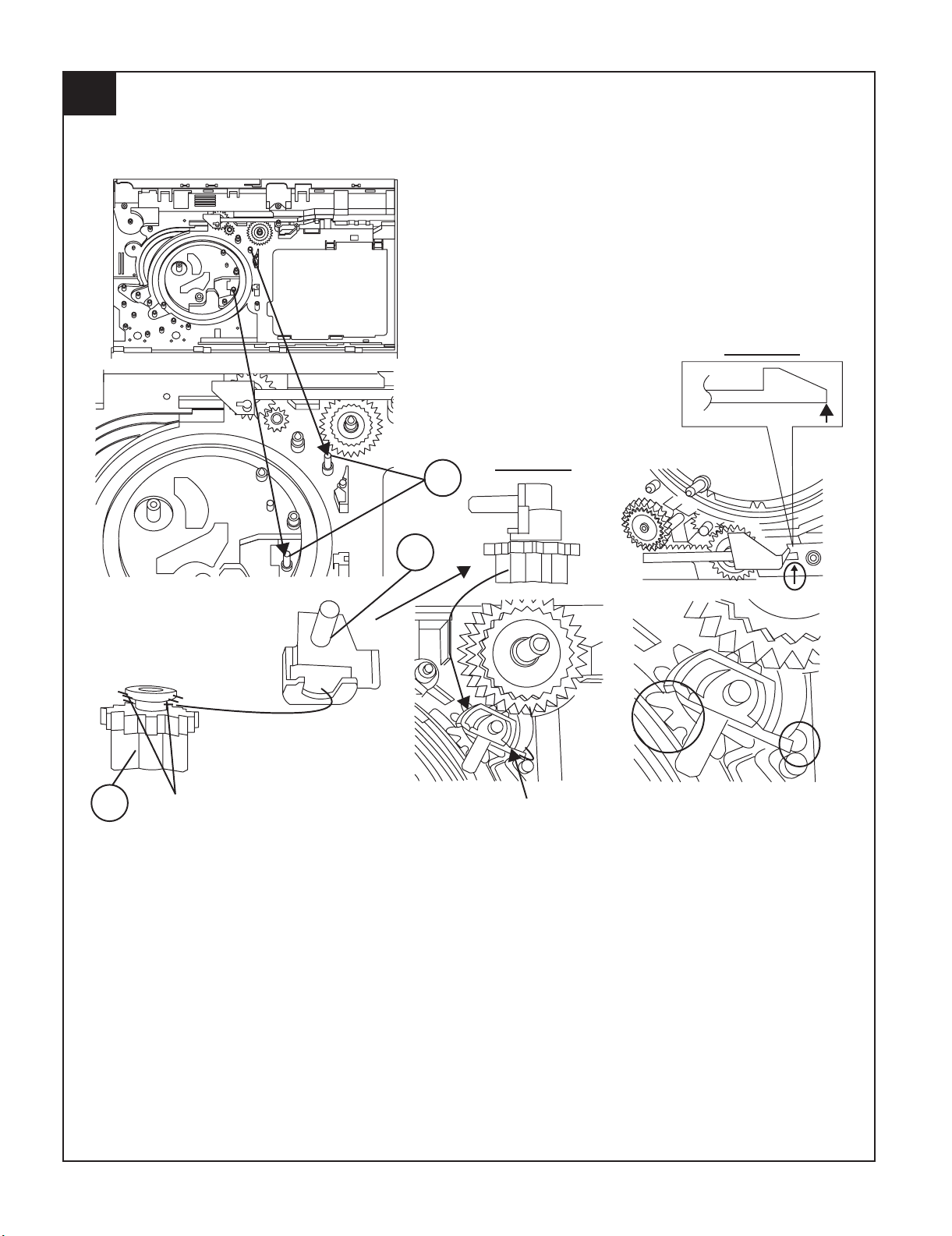
Page 12
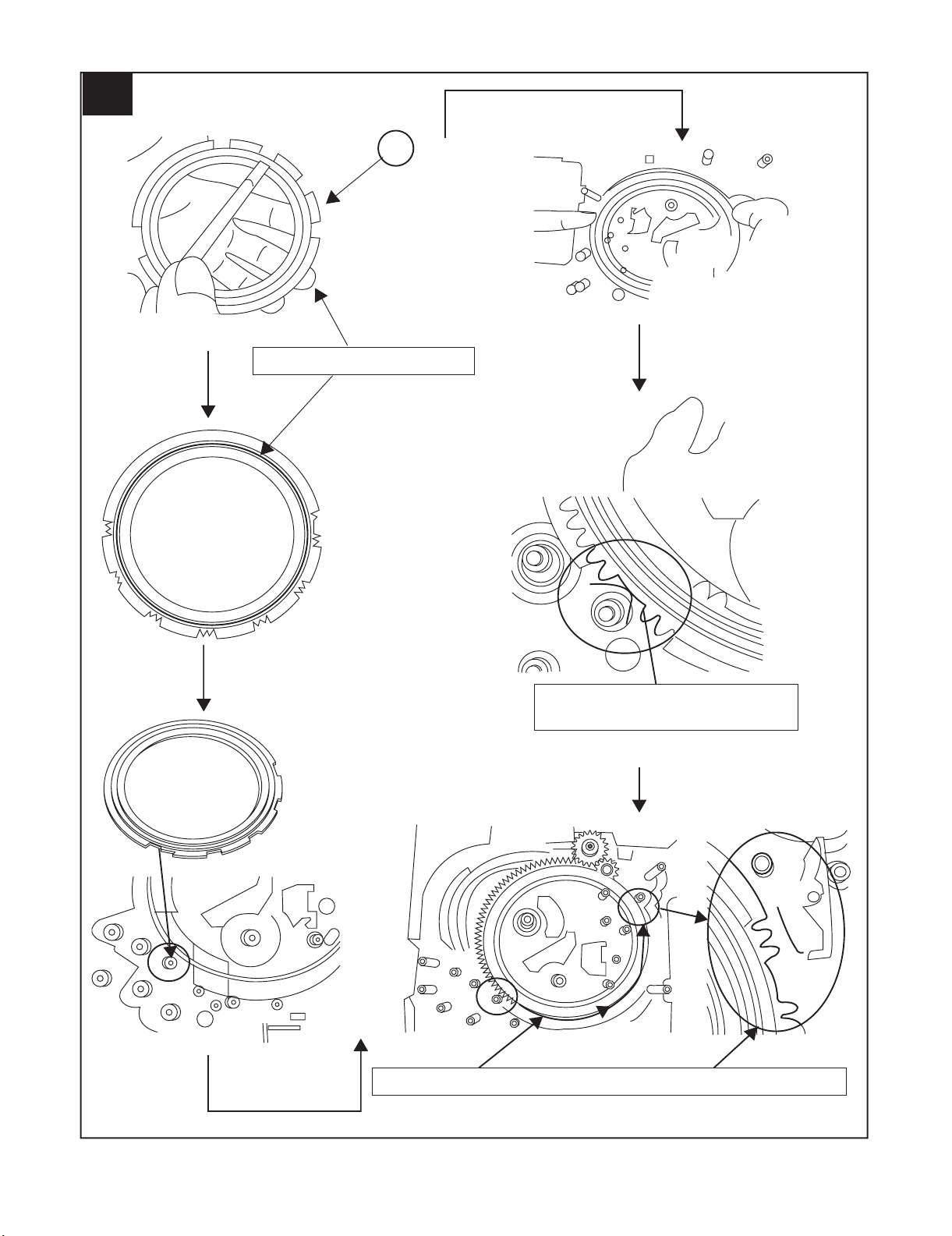
CD-SW200E
2
139
APPLY SANKOL BEFORE FIX
FIX ITEM 1 ACCORDING TO THE
SHOWN PICTURE ABOVE
ROTATE MODE BIG GEAR UNTIL REACH AS SHOWN IN PICTURE
2 – 6
Page 13
3
CD-SW200E
143
APPLY GREASE
112
PULL THE LEVER UNITIL
REACH THE ARROW MARK
2 – 7
Page 14
CD-SW200E
4
FIGURE 2
FIGURE 1
152
142
APPLY GREASE
118
SLOT CLAMP SW ARM INSIDE BASE SLOT
2 – 8
Page 15
5
CD-SW200E
APPLY GREASE AT BOTTOM SIDE
OF GEAR FOLLOW MARKING
NO NEED APPLY GREASE AT BOTTOM
SIDE
FIGURE 1
APPLY GREASE AT
TOP SIDE OF GEAR
FOLLOW MARKING
127
OTHER THAN FIGURE 1 DIRECTION ALL N.G
O.K
128
N.G
BLACK MARK
2 – 9
Page 16
CD-SW200E
6
APPLY GREASE AT
HALF GEAR AREA
ROTATE CLOCKWISE UNTIL REACH HERE (MAXIMUM)
129
2 – 10
Page 17
7
CD-SW200E
CHANGE COLOR TO BLACK
150151148
2 – 11
Page 18
CD-SW200E
8
TRAY BIG GEAR
CHANGE COLOR
TO BLACK
MUST FREE FROM GREASE THE SHOWN AREA
O.K
GREASE APPLICATION LENGTH
GREASE APPLICATION PORTION
N.G
124
TRAY BIG GEAR
CHANGE COLOR
TO BLACK
SHOWN HOLE MUST FACING ARROW DIRECTION
131
2 – 12
Page 19

9
CD-SW200E
138 126 125
APPLY GREASE AT
BOTTOM SIDE ONLY
TR-RE JOINT GEAR C
APPLY GREASE ONLY AT TOP SIDE GEAR
MUST FIX ACCORDING TO T HE HOLE'S
2 – 13
Page 20

CD-SW200E
10
148 147 146 145
2 – 14
Page 21

11
CD-SW200E
121
144
WHEN FIXING ITEM 2 MUST FOLLOW AS SHOWN
APPLY GREASE
130
2 – 15
Page 22

CD-SW200E
12
117
FIGURE 2
FIGURE 1
APPLY GREASE
FIGURE 3
APPLY GREASE SC141
2 – 16
Page 23

13
CD-SW200E
ITEM 2 , 3 MUST APPLY GREASE ON TOP SIDE GEAR ONLY
134
GEAR 112 GEAR 112
133
132
O.K
TOP VIEW AFTER
ASSY
N.G
FIX REVERSE N.G
2 – 17
Page 24

CD-SW200E
14
APPLY GREASE BEFORE FIX
A
MOVE 112 UNTIL TOUCH THE WALL
B
DURING GEAR A ROTATE
MUST PRESS SHOWN AREA
AND LEVER B WILL MOVE
ARROW DIRECTION THEN
FIX PART 108
SCREW TORQUE
+0.5
2 kgf-cm
-0
108 803 x6
APPLY GREASE
CONFIRM WHETHER
FIXED
PROPELY OR NOT
2 – 18
Page 25

15
CD-SW200E
APPLY GREASE
115
BEHIND THE LEVER NEED TO APPLY GREASE
PULL IT THEN LEVER WILL
MOVE IN
2 – 19
Page 26

CD-SW200E
16
123
115
APPLY GREASE
APPLY GREASE BEFORE FIX
APPLY GREASE
AT BOSS
SPRING MUST ARRANGE UNDER THE HOOK
BOARD R
BOARD R
O.K LR JOINT LEV
LR JOINT LEV
N.G
2 – 20
Page 27

17
CD-SW200E
ASSY REVERSELY N.G
103 137 136
APPLY GREASE
BIG SLOT MUST FACING OUT
WHEN FIX & AFTER FIX TO BASE CHASSIS
AFTER ASSY CONFIRM THE FREE DROP
GEAR POSITION DURING FIXING
2 – 21
Page 28

CD-SW200E
18
ASSY REVERSELY N.G
APPLY GREASE
114
135
136
BIG SLOT MUST FACING OUT
WHEN FIX & AFTER FIX TO BASE CHASSIS
AFTER ASSY CONFIRM THE FREE DROP
GEAR POSITION DURING FIXING
CONFIRM BOTH GEAR SIT PROPELY & LOCKED
2 – 22
Page 29

19
CD-SW200E
AFTER FIX OUTER UP/DOWN LEVER HOLD SHOWN PORTION AND
MOVE UP/DOWN THEN CONFIRM LEVER GO INSIDE THE HOLE OR NOT
120
BIGGER SLOT FACING OUT
IF GO INSIDE HOLE
IS O.K
IF NO GO INSIDE HOLE IS N.G
119
BIGGER SLOT FACING OUT
2 – 23
Page 30

CD-SW200E
20
BIG SLOT FACING OUT
110
2 – 24
Page 31

21
CD-SW200E
PUSH THE LEVER ACCORDING TO ARROW
DIRECTION THEN FIX
WHEN FIX MAIN BASE ASSY FOLLOW ACCORDING TO O.K PICTURE
MAKE SURE MECHA HOLDER SHAFT FIX PROPELY TO LEVER
O.K
N.G
N.G
2 – 25
Page 32

CD-SW200E
22
APPLY SANKOL
101
102
APPLY SANKOL AT TRAY SLIDING PORTION
APPLY SANKOL ON TOP
FIX TRAY NO 1 FIRST THAN
FOLLOW OTHER
APPLY SANKOL INSIDE THE SLOT
& OTHER SHOWN PORTION
RIB
RIB
COSMO GUIDE TRAY HAVE
MARKING AS SHOWN
2 – 26
Page 33

23
GEAR UP/DOWN BOARD
111
APPLY GREASE AT INNER & OUTER GEAR SLIDING PORTION
WH EN FIX GEAR UP/
DOWN BOARD THE
TWO LEVER MUST AT
PARALLEL LINE &
POSITION AT TOP
MAX SIDE
CD-SW200E
2 – 27
AFTER ASSY GEAR UP/DOW N BOARD
Page 34

CD-SW200E
24
SCREW TORQUE
+0.5
3 kgf-cm
-0
2 – 28
804
Page 35

25
CD-SW200E
AFTER ASSY TOP PLATE
FIX THE FFC
FFC4
AFTER PUSH MAKE SURE SNAP PROPELY
AFTER FIX PUSH FOLLOW ARROW DIRECTION
BEFORE LOCK
AFTER LOCK
BACK
PORTION
107
122
BEFORE LOCK
PRESS IN
SLOT IN
BEFORE LOCK
AFTER LOCK
AFTER LOCK
MUST CONFIRM
MUST CONFIRM
2 – 29
Page 36

CD-SW200E
26
O.K
N.G
CAUTION
1. MAKE SURE NO PW B CHIP INSIDE SET .( BEFORE
FIX MAKE SURE PW B NO DUST , GREASE & ETC )
803
2 – 30
Page 37

27
THE TWO SLOT
MUST FREE FROM GREASE
APPLY GREASE BELOW
THE MARKING FOR
BOTH PORTION
CD-SW200E
ASSEMBLY SEQUENCE
1. APPLY GREASE TO MAIN BASE
GREASE APPLICATION AREA
ALL BOSS
APPLY GREASE
APPLY GREASE
CAUTION
TRAY SLIDING
AREA MUST
FREE FROM
GREASE
APPLY GREASE
APPLY GREASE AT WALL
APPLY GREASE
APPLY GREASE
APPLY GREASE
AT BOTH SLOT
105
APPLY GREASE AT 3 HALF MOON
1 RIB ONLY
APPLY GREASE
APPLY GREASE
INSIDE SLOT
2 – 31
Page 38

CD-SW200E
28
REFERENCE ONLY
MOTOR GEAR HEIGHT FROM
MAIN BASE 12.2
+
0.1
-
0.1
-
+
12.2
MOTOR SCREWING HOLE
MUST HAVE GAP
M1,2
801
-0
13.8 + 0.2
SCREW TORQUE
1.5 + 0.5
-0
AFTER SCREW MOTOR,CONFIRM THE
ARRANGEMENT AS IN FIGURE 2
FIGURE 2
APPLY GREASE
2 – 32
Page 39

29
APPLY SANKOL
CD-SW200E
3.1 + 0.1
SHAFT X 3 DIM AFTER INSERTION
MUST CONFIRM EVERYDAY
SANKOL APPLICATION AREA
109-2
APPLY GREASE AT THE SLIDING PORTION
114
116
UP / DOWN
HOLDER CHANGE
TO NATURE
COLOR
APPLY GREASE
2 – 33
Page 40

CD-SW200E
30
BEFORE MELT IT
AFTER MELT IT ( MUST FLAT )
CHANGE COLOR
TO NATURE
WHEN FITTING STABILIZER PLATE TO STABILIZER,
ROTATE STABILIZER ANTI CLOCKWISE BY JIG
( BY HAND CANNOT X )
BELOW
AFTER ASSY TO HOLDER
STABILIZER NEED CLEAN
WITH ALCOHOL DISC
TOUCHING SURFACE
2 – 34
Page 41

31
CD-SW200E
104
APPLY GREASE
MUST MAKE SURE SNAP PROPELY BOTH SIDE
ALL SURFACE MUST TOUCH
O.K N.G
GAP
N.G
2 – 35
Page 42

CD-SW200E
32
NO GAP HAVE GAP
O.K N.G
2 – 36
Page 43

CD-SW200E
AudioCD-SW200EService ManualCD-SW200EMarketE
CHAPTER 3. MECHANISM BLOCKS
[1] Caution on diassembly
Caution on Disassembly
Follow the below-mentioned notes when disassembling the unit and reassembling it, to keep it safe and ensure excellent performance:
1. Take cassette tape and compact disc out of the unit.
2. Be sure to remove the power supply plug from the wall outlet before starting to disassemble the unit.
3. Take off nylon bands or wire holders where they need to be removed when disassembling the unit. After servicing the unit, be sure to rearrange
the leads where they were before disassembling.
CD-SW200E
STEP
Note 1:
After removing the connector for the optical pickup from the
connector, wrap the conductive aluminium foil around the
front end of the connector so as to protect the optical
pickup from electrostatic damage.
REMOVAL PROCEDURE
1 Top/Side Cabinet 1. Screw .................... (A1) x14
2 Changer Unit/ 1. Screw ...................... (B1) x2
Rear Panel B 2. Hook ........................ (B2) x2
3
Rear Panel A with
Fan motor 2. Socket ..................... (C2) x1
4 Main/Tuner PWB 1. Screw ...................... (D1) x2
5 Front Panel 1. Screw ...................... (E1) x2
6 Tape Mechanism 1. Op e n the c a ss e tt e Cove r
7 Display PWB 1. Knob ........................ (G1) x1
3. Flat Cable................ (B3) x1
4. Socket ..................... (B4) x1
1. Screw ......................
2. Flat Cable ............... (D2) x1
3. Socket ..................... (D3) x4
4. Flat Wire .................. (D4) x1
5. Screw ...................... (D5) x5
2. Socket (E2) x1
3. Hook ........................
2. Screw ....................... (F1) x6
3. Flat Cable ................(F2) x1
2. Screw .................... (G2) x10
3. Hook (G3) x5
.....................
........................
(C1) x9
(E3) x2
8 Game Input PWB 1. Screw...................... (H1) x2
9 CD Servo PWB 1. Screw ....................... (J1) x3
10 Changer 1. Screw ...................... (K1) x4
Mechanism Unit 2. Changer Chassis .... (K2) x1
2. Flat Cable ................ (J2) x2
3. Socket ...................... (J3) x1
4. Hook ......................... (J4) x1
11 CD Mechanism 1. Screw ....................... (L1) x4
(C2)x1
Rear
Panel B
(B1)x2
M3x10mm
Rear
Panel A
Fan Motor
Main PWB
(C1)x9
M3x10mm
(B2)x1
Pull
Changer
Mechanism
Unit
(D3)x2
(D2)x1
(D3)x1
(E2)x1
CD Servo
PWB
Main PWB
(D1)x2
M3x10mm
Front Panel
(B2)x1
Pull
(B3)x1
(B4)x1
Lug Wire
(A1)x3
M3x10mm
Rear Panel B
Rear Panel A
Top/Side Cabinet
(A1)x8
M3x10mm
Front Panel
(A1)x3
M3x10mm
3 – 1
(E3)x1
(D4)x1
(D3)x1
Power PWB
(D5)x4
M3x10mm
(E1)x2
M3x8mm
Main
PWB
Front Panel
Tuner
PWB
(D5)x1
M3x10mm
(E3)x1
Main
PWB
Page 44

CD-SW200E
Tape
Mechanism
Lug Wire
(F1)x6
M3x10mm
Lug Wire
(F2)x1
Front Panel
Open
Cassette
Cover
(K1)x4
M3x10mm
(K2)x1
(G2)x10
M2.6x10mm
(J2)x1
(H1)x2
M3x10mm
(J1)x3
M3x10mm
(J3)x1
(J4)x1
Front Panel
Display PWB
(G3)x5
(J2)x1
(G1)x1
Game Input
PWB
(L1)x4
M2.6x10mm
CD Mechanism
Changer
Mechanism
Unit
Changer
Mechanism
Unit
CD Servo
PWB
Changer
Mechanism
Unit
3 – 2
Page 45

CD-SW200E
CP-S200H
STEP
REMOVAL PROCEDURE
1 Woofer (A1) x1
2 Tweeter 1. Screw ...................... (B1) x2
3 Super Tweeter 1. Screw ...................... (C1) x2
Screwdriver
Driver should
be pried away
from Speaker Box.
1. Front Panel .............
......................
2. Screw (A2) x4
(A1)x1
Speaker Box
Speaker Box
CP-SW200E
STEP
1 LED PWB (A1) x1
2 Woofer 1. Screw ...................... (B1) x8
Screwdriver
Driver should
be pried away
from Speaker Box.
Front Panel
REMOVAL PROCEDURE
1. Front Panel .............
2. Socket (A2) x1
3. Screw (A3) x2
(A1)x1
....................
......................
Speaker Box
Super Tweeter
Woofer
Tweeter
(B1)x2
M3x10mm
(C1)x2
M3x10mm
(A2)x4
M4x16mm
(B1)x8
M4x16mm
Woofer
Speaker Box
LED PWB
(A2)x1
(A3)x2
M2.6x10mm
3 – 3
Page 46

CD-SW200E
[2] Removing and reinstalling the main parts
1. TAPE MECHANISM SECTION
Perform steps 1 to 5 and 6 of the disassembly method to remove the
tape mechanism. (See page3-1, 3-2)
1.1. How to remove the record/playback and erase heads
(TAPE 2) (See Fig. 1)
1. When you remove the screws (A1) x 2 pcs., the recording/playback head and three-dimensional head of the erasing head can be
removed.
TAPE 2
Clutch Ass'y
Record/Playback
Head
Pinch
Pinch Roller
(C1)x1
Pull
<B>
<A>
Roller
Pawl
Figure 3
1.4. How to remove the belt (TAPE 2) (See Fig. 4)
1. Remove the main belt (D1) x 1 pc., from the motor side.
2. Remove the FF/REW belt (D2) x 1 pc.
Erase Head
(A1)x2
φ2x9mm
Figure 1
1.2. How to remove the playback head (TAPE 1)(See Fig. 2)
1. When you remove the screws (B1) x 2 pcs., the playback head can
be removed.
TAPE 1
(B1)x2
φ2x9mm
Figure 2
Clutch Ass'y
Playback
Head
1.5. How to remove the belt (TAPE 1) (See Fig. 4)
1. Remove the main belt (E1) x 1 pc., from the motor side.
2. Remove the FF/REW belt (E2) x 1 pc.
Tape
Motor
TAPE 2
Main Belt
(D1)x1
TAPE 1
Main Belt
(E1)x1
TAPE 1
FF/REW
Belt
(E2)x1
TAPE 2
FF/REW
Belt
(D2)x1
Main Belt
(D1)x1
Main Belt
(E1)x1
Tape
Motor
Figure 4
1.6. How to remove the motor (See Fig. 5)
1. Remove the screws (F1) x 2 pcs., to remove the motor.
Tape
Motor
Clutch Ass'y
1.3. How to remove the pinch roller (TAPE 1/2) (See Fig. 3)
1. Carefully bend the pinch roller pawl in the direction of the arrow
<A>, and remove the pinch roller (C1) x 1 pc., in the direction of the
arrow <B>.
Note:
When installing the pinch roller, pay attention to the spring mounting
position.
(F1)x2
φ2.6x5mm
Figure 5
3 – 4
Page 47

2. CD MECHANISM SECTION
Mark 1
(DISC 1)
(DISC 2)
(DISC 3)
(DISC 4)
(DISC 5)
Gear up down board
Mark 3 Mark 5
Mark 2 Mark 4
Perform steps 1, 2, 9, 10 and 11 of the disassembly method to remove
the CD mechanism. (See page 3-1, 3-2)
2.1. Remove the pickup. (See Fig. 1)
1. Remove the stop washer (A1) x 1 pc., to remove the gear (A2) x 1
pc.
2. Remove the screws (A3) x 2 pcs., to remove the shaft (A4) x 1 pc.
3. Remove the pickup.
Note
After removing the connector for the optical pickup from the connector
wrap the conductive aluminium foil around the front end of connector
so as to protect the optical pickup from electrostatic damage.
(A3)x2
φ2.6x6mm
CD Mechanism
Shaft
(A4)x1
Gear
(A2)x1
CD-SW200E
Reduction gear C
Front Rear
Figure 3
2. In another case, if CD mechanism is at tray No.1 play position and
to remove CD located in tray No.3, the procedure is as follows:
If the gear up down board is located at tray No.1 position, then
rotate gear clock-wise until it at stock position. Rotate reduction
gear D clockwise (Figure 4) to move the CD mechanism to tray
No.3 position.This is confirmed by checking the gear up down
board position by the marking as indicated on the main chassis as
shown in Figure 5.
Reduction gear D
Stop Washer
(A1)x1
Pickup Unit
Figure 1
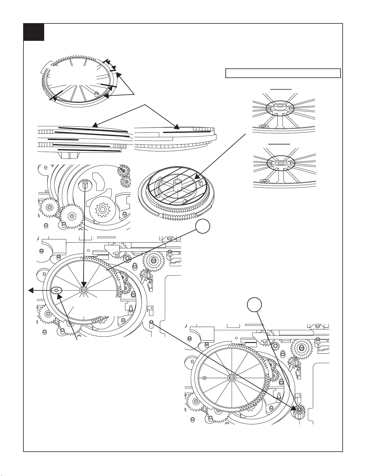
3. CHANGER MECHANISM SECTION
Perform steps 1, 2, 9 and 10 of the disassembly method to remove the
CD changer mechanism.
3.1. How to remove CD Disc (See Fig. 2~5)
1. When CD is at play position (Figure 2), rotate reduction gear C
clock-wise as shown in Figure 3 until disc tray is at stock position,
then rotate further to eject the disc tray so that CD can be removed
from the tray.
CD Disc
Disc Tray
Guide Tray
CD At play position.
CD Disc
Up Down
Figure 4
Figure 5
Figure 2
CD At stock position.
3 – 5
Page 48

CD-SW200E
3.2. How to Remove the tray motor/main cam motor/5Changer Motor PWB (See Fig. 6)
1. Remove the screws (A1) x 2 pcs., to remove tray motor/main cam
motor/5-Changer Motor PWB.
Changer Mechanism Unit
Main Cam Motor
(A1)x2
φ2x10mm
Figure 6
NOTE: There are 2 more screws tighten the motors at the bottom of
main chassis. Before performing procedure 1 above, disc stop
spring, top plate gear up down board and trays must be
removed, then only the 2 screws can be untighten.
Tray Motor
5-Changer
Motor PWB
3 – 6
Page 49

AudioCD-SW200EService ManualCD-SW200EMarketE
CHAPTER 4. DIAGRAMS
[1] Block diagrams
CD-SW200E
XL1
16.9344 MHz
+3.3V
CONSTANT
VOLTAGE
TO MAIN SECTION
R-CH
AGND
L-CH
CE
43
CL
44
DI
45
DO
46
RESB
47
INTB0
48
INTB1
49
XOUT
72
XIN
73
DVDD
AVDD
36 41
+3.3V
D_+5V(+B5)
DGND
7875
LCHO
+8V(+B7)
MGND
7123 45 6
CNP3
RCHO
LC78690E
CD SERVO
XVDD
74
LRVDD
76 876521
IC1
Q1
TO DISPLAY SECTION
+B6
GND
PHOTO
MO_A-
DIN
BIN
CIN
AIN
LASER
DRIVER
CD_RESB
MO_A+
CONT1
EIN
1413
CD_CLK
5251
CONT0
FIN
CD_DI
CD_DO
LDS
CD_CE
MP3_INT11CD_INT12TRAY SW1/SW2
10
PUIN
SLDO
SPDO
FDO
TDO
LDD
181968
13
77
71
67
57
56
55
54
53
42
40
37
26
20
32
24
25
22
23
DISC/CLAMP
14319876524
CNP7
+5V
SW3 TRAY SW2
SW2 TRAY SW1
SW1 CLAMP
SW4 DISC
RX1
GND
17151311
22
23
VIN4
VIN3
VIN2
VIN1
28
PVCC2
REV6
IC2
FWD6
LA6261
FOCUS/TRACKING/
9
27
SPIN/SLIDE
DRIVER
M1
M1
MAIN CAM
TRAY MOTOR
M
M
+
+
--
10 11319876524
32 3331 34
VO6-
VO6+
VO5+
FWD5
REV5
MOTOR
CNP4
VO5-
19
20
30
7
26
PICKUP UNIT
+3.3V
COIL
TRACKING
FOCUS COIL
Figure 4-1 BLOCK DIAGRAM (1/3)
4 – 1
NM1
SPINDLE
MOTOR
NM2
SLED
MOTOR
M
M
4
3363521
56
NSW 1
PICKUP
IN
Page 50

CD-SW200E
VF
8
N
W
SO301
FM ANTENNA
TERMINAL
AM LOOP
ANTENNA
CNP302
FROM CD SECTION
TAPE 1
P.B. HEAD
TAPE 2
REC./P.B.
HEAD
CNP2
L-CH
R-CH
L-CH
R-CH
ERASE
HEAD
FE301
FM FRONT END
8
2
4
VT
AM
TRACKING
+B4
T303 T306
1
2
3
REC.
P.B.
AC BIAS
3
6
7
AM BAND
COVERAGE
BI601CNS601
1
3
4
SWITCHING
Q101~
Q104
Q105
Q106
1
CF301
5
LC72131
(TUNER)
JK691
VIDEO OUT
L(T1)
R(T1)
L(T2)
R(T2)
POP REDUCE
LREC.
R REC.
SWITCHING
+B4
Q112
Q111
L103
BIAS
OSC
FM IF
AMP.
Q301
IC302
PLL
VCC
Q360
SWITCHING
1
P.B.
24
2
23
6
T1/T2
REC
9
16
11
12
NOR/
15
HIGH
T1/T2
Q114
SWITCHING
SWITCHING
SWITCHING
CF302
T351
AM IF
21
AM MIX
21
AM OSC IN
AM OSC OUT
AM RF IN
X352
4.5 MHz
20 22 11
AOUT
+B4
FM
JK690
GAME INPUT
L
R
VIDEO
13
4
21
H/N
7
18
1615
XIN
XOUT
7
AUX
+B4
L
P.B.
R
REC.RL
IC101
AN7345K
10
19
Q113
Q109
PLAYBACK AND RECORD/
ALC
PLAYBACK AMP.
+B4
Q110
BIAS
+B3
+B3
450 kHz
CF352
4
GND
AM IF
FM/AM
OUT
18
7
L354
LOW PASS LOW
IC303
STEREO
LA1832S
FM IF DET./
FM MPX./AM IF
CLK
DO
DI
CE
5413
6
MO/ST
FM/AM
21
9 10
+B4
9
L
16
R
L
10
TAPE
15
R
L
CD
+B4
MOTOR
DRIVER
Q709~
Q711
Q703~
Q708
DRIVER
11
14
AUDIO PROCESSOR
R
L
12
13
R
7
TUNER
SOLENOID
10.7 MHz
CF351
17
985
FM
DET
FM+B
MPX IN
162324
+B4
17
LED503
LED505
23
IC601
LC75341
18
MUTING
LED701
MECHANISM
456 kHz
VCO
PHASE
(FM/AM)
12
+B8
3
Q107
Q108
TAPE
ASS'Y
X351
13
MO/ST
14
15
DRIVER
L
R
IC503
7
KIA4558F
PRE AMP.
5
1
DI
2
CE
24
CLK
21
4
LED
Q702
ZD351
5.1V
3
-20dB
ATT
R
L
LR
24 23 21 22
43
MICROCOMPUTER
+B4
Q608
REC/PLAY
IC603
IXA043AW
SOUND
JOG701
VOLUME
5
IC701
IXA072AW
SYSTEM
(2/2)
Q607
T1/T2
BIAS
MUTE
SYSTEM
VF1
U
S
+B
Figure 4-2 BLOCK DIAGRAM (2/3)
4 – 2
Page 51

S
FL701
FL DISPLAY
812 45
26
25
~
CD-SW200E
47
~
+B8
5150
TAPE
MECHANISM
ASS'Y
+B8
MUTE
SYSTEM
SP DET.
D901~D906
IC901, IC902
STK412-490
POWER AMP.
18
L
14
R
7
1
5
2
6
-B1
26 3837 394055
57
~
78
80
VLOAD
79
VDD
IC701
IXA072AW
SYSTEM
MICROCOMPUTER
AVDD
1 54515253
L-OUT
R-OUT
1011
RESET
Q712
Q901~
Q908
(1/2)
RESET
16 1742 1312 20 23 28 29 30 31
XL701
8.3886 MHz
11
8
+B1
81
~
98
99
100
+B8
+B8
SP RELAY
ON-OFF
D801
18
VDD
~
15 14
AVDD
CLK
CEDIDO
Q905
RL901,
RL902
27
3
+B8
41
2
~~
4
34
32
25
36
Q910
DRIVER
FAN MOTOR
RX701
REMOTE
SW701-SW707
SW709-SW716
SW724-SW734
1
SENSOR
2
KEY
TO CD
SECTION
+B5
M901
M
MOTOR
SO901
SPEAKER
TERMINAL
SO902
SUBWOOFER
TERMINAL
+B3
JK692
HEADPHONES
PT801
MAIN POWER
TRANSFORMER
+B8
FAN
-B2
+B2
D802
VOLTAGE
F802
T5AL250V
F801
T5A L 250V
REGULATOR
M+13V
+B3
IC808
KTC2026
VF2
VF1
-VF
+B7
LD+8V
UN
SW_5.6V
+B8
IC802
31
KIA78L05
E
+B5
+B6
+B4
C
A+10V
A5V
SW5V
IC807
3
KIA7812AP
IC806
3
KIA7812AP
VOLTAGE
REGULATOR
1
1
D803,
D804
T2A L 250V
T2A L 250V
Q801
REGULATOR
F804
F803
VOLTAGE
T.F.
F805
T4A L 250V
L890LINE
FILTER
AC POWER
SUPPLY CORD
AC 230-240 V, 50 Hz
VOLTAGE
REGULATOR
VOLTAGE
REGULATOR
IC805
3
KIA7805AP
1
Figure 4-3 BLOCK DIAGRAM (3/3)
4 – 3
Page 52

CD-SW200E
KRA107 S
KRC102 S
KRC104 S
KTA1504 GR
KTA1504 Y
KTC3875 GR
B
(3)
E
(1)
C
(2)
TOP
VIEW
KTC2026
KTA1266 GR
KTA1271 Y
KTA1273 Y
KTA1274 Y
VIEW
FRONT
ECB
VIEW
FRONT
ECB
(S)(G)(D)
(1)(2)(3)
TS20P05G
TS10B05G
AC AC
VIEW
FRONT
FRONT
VIEW
SDPB40F2A
SLR342VCB1
SDPB50CD
KTC3200 GR
KTC3203 Y
KTC3205 Y
2SC280 O
AudioCD-SW200EService ManualCD-SW200EMarketE
CHAPTER 5. CIRCUIT DESCRIPTION
[1] Notes on schematic diagram
•Resistor:
To differentiate the units of resistors, such symbol as K and M are
used: the symbol K means 1000 ohm and the symbol M means
1000 kohm and the resistor without any symbol is ohm-type resistor. Besides, the one with “Fusible” is a fuse type.
• Capacitor:
To indicate the unit of capacitor, a symbol P is used: this symbol P
means pico-farad and the unit of the capacitor without such a symbol is microfarad. As to electrolytic capacitor, the expression
“capacitance/withstand voltage” is used.
(CH), (TH), (RH), (UJ): Temperature compensation
(ML): Mylar type
(P.P.): Polypropylene type
• Schematic diagram and Wiring Side of P.W.Board for this model are
subject to change for improvement without prior notice.
• The indicated voltage in each section is the one measured by Digital Multimeter between such a section and the chassis with no signal given.
1. In the tuner section,
indicates AM
indicates FM stereo
2. In the main section, a tape is being played back.
3. In the deck section, a tape is being played back.
( ) indicates the record state.
4. In the power section, a tape is being played back.
5. In the CD section, the CD is stopped.
• Parts marked with “ “ ( ) are important for maintaining the safety of the set. Be sure to replace these parts with
specified ones for maintaining the safety and performance of the
set.
REF. NO DESCRIPTION POSITION
JOG701 VOLUME ON—OFF
NSW1 PICKUP IN ON—OFF
SW1 CLAMP ON—OFF
SW2 TRAY SW1 ON—OFF
SW3 TRAY SW2 ON—OFF
SW4 DISC ON—OFF
SW701 POWER ON/STAND-BY ON—OFF
SW702 CLOCK/TIMER ON—OFF
SW703 TUNING UP ON—OFF
SW704 TUNING DOWN ON—OFF
SW705 FAST REWIND/PRESET DOWN ON—OFF
SW706 EQUALIZER ON—OFF
SW707 FAST FORWARD/PRESET UP ON—OFF
SW712 TUNER (BAND) ON—OFF
[2] Types of transistor and LED
REF. NO DESCRIPTION POSITION
SW713 CD ON—OFF
SW714 TAPE ON—OFF
SW715 GAME/VIDEO ON—OFF
SW716 X-BASS/DEMO ON—OFF
SW724 PLAY ON—OFF
SW725 STOP ON—OFF
SW726 REC./PAUSE ON—OFF
SW727 MEMORY/SET ON—OFF
SW728 OPEN/CLOSE ON—OFF
SW729 DIRECT PLAY ON—OFF
SW730 DISC2 ON—OFF
SW731 DISC4 ON—OFF
SW732 DISC5 ON—OFF
SW733 DISC3 ON—OFF
SW734 DISC1 ON—OFF
5 – 1
Page 53

[3] Waveforms of CD circuit
CD-SW200E
5 – 2
Page 54

CD-SW200E
[4] Voltage
VOLTAGE PIN VOLTAGE PIN VOLTAGE PIN VOLTAGE PIN VOLTAGE PIN VOLTAGE PIN VOLTAGE
IC301
1 51.12 V 1 4.97 V 1 0.91 V 1 0.00 V 1 4.94 V 51 0.00 V 1 17.22 V
2 20.47 V 2 4.97 V 2 1.62 V 2 0.00 V 2 4.94 V 52 4.40 V 2 0.00 V
3 6.20 V 3 4.97 V 3 5.22 V 3 0.00 V 3 4.92 V 53 4.38 V 3 4.87 V
4 6.04 V 4 0.00 V 4 1.59 V 4 4.96 V 4 4.92 V 54 0.00 V
5 20.47 V 5 0.00 V 5 0.00 V 5 4.93 V 5 1.32 V 55 4.39 V
6 51.09 V 6 4.97 V 6 5.24 V 6 4.94 V 6 4.92 V 56 4.43 V PIN VOLTAGE
7 0.00 V 7 4.97 V 7 4.50 V 7 4.94 V 7 4.92 V 57 -29.05 V 1 16.67 V
8 0.00 V 8 5.00 V 8 5.20 V 8 4.94 V 8 0.267 V 58 -26.42 V 2 0.00 V
9 0.00 V 9 4.97 V 9 5.24 V 9 4.94 V 9 4.87 V 59 -18.41 V 3 9.91 V
10 0.00 V 10 4.97 V 10 4.94 V 10 4.87 V 60 -29.08 V
11 0.00 V 11 4.97 V 11 4.94 V 11 4.87 V 61 -29.08 V
12 49.67 V 12 0.00 V 12 4.93 V 12 0.00 V 62 0.00 V PIN VOLTAGE
13 49.81 V 13 9.90 V PIN VOLTAGE 13 4.94 V 13 0.00 V 63 -29.08 V 1 17.21 V
14 0.14 V 14 4.97 V 1 2.64 V 14 4.94 V 14 0.00 V 64 -0.92 V 2 1.32 V
15 0.15 V 15 4.96 V 2 0.00 V 15 4.94 V 15 0.00 V 65 -0.96 V 3 13.24 V
16 48.45 V 16 0.00 V 3 0.00 V 16 4.94 V 16 0.00 V 66 -11.10 V
17 0.15 V 17 0.00 V 4 0.00 V 17 4.92 V 17 0.00 V 67 0.00 V
18 0.15 V 18 4.96 V 5 0.00 V 18 4.94 V 18 0.00 V 68 -23.60 V PIN VOLTAGE
IC902
PIN VOLTAGE 22 4.97 V 9 0.00 V 22 4.96 V 22 4.52 V 72 0.00 V
1 51.12 V 23 4.95 V 10 0.00 V 23 9.91 V 23 4.41 V 73 -23.60 V
2 20.47 V 24 0.00 V 11 5.10 V 24 0.00 V 24 4.54 V 74 -26.20 V
3 6.25 V 12 0.00 V 25 0.00 V 75 -23.60 V
4 6.04 V 13 5.10 V 26 0.00 V 76 0.00 V
5 20.47 V
6 51.10 V PIN VOLTAGE 15 0.00 V PIN VOLTAGE 28 4.05 V 78 0.00 V
7 0.00 V 1 0.00 V 16 2.59 V 1 2.07 V 29 4.07 V 79 -23.60 V
8 0.00 V 2 0.00 V 17 5.12 V 2 5.03 V 30 0.00 V 80 0.00 V
9 0.00 V 3 0.56 V 18 0.00 V 3 2.07 V 31 4.66 V 81 -23.61 V
10 0.13 V 4 1.94 V 19 0.00 V 4 0.00 V 32 0.23 V 82 -20.84 V
11 0.13 V 5 0.00 V 20 9.89 V 5 5.11 V 33 4.95 V 83 -10.43 V
12 49.61 V 6 1.32 V 21 0.00 V 6 5.11 V 34 4.95 V 84 -23.50 V
13 49.86 V 7 0.00 V 22 2.58 V 7 4.06 V 35 0.00 V 85 -26.40 V
14 0.15 V 8 0.59 V 8 5.03 V 36 0.00 V 86 -28.93 V
15 0.15 V 9 3.36 V 9 0.00 V 37 13.15 V 87 -26.40 V
16 48.48 V 10 3.34 V 10 3.89 V 38 13.15 V 88 -21.10 V
17 0.00 V 11 0.00 V 11 3.89 V 39 13.15 V 89 -25.12 V
18 0.00 V 12 0.00 V 12 3.89 V 40 0.00 V 90 -24.99 V
1 1.56 V 21 3.20 V 41 3.21 V 61 3.10 V 3 2.04 V 26 0.00 V
2 1.69 V 22 1.62 V 42 0.00 V 62 1.53 V 4 2.03 V 27 4.77 V
3 1.67 V 23 1.61 V 43 0.00 V 63 0.00 V 5 2.03 V 28 7.69 V
4 1.52 V 24 1.61 V 44 2.97 V 64 0.00 V 6 2.04 V 29 4.74 V
5 1.62 V 25 1.62 V 45 2.94 V 65 0.00 V 7 0.00 V 30 0.00 V
6 1.62 V 26 0.00 V 46 0.93 V 66 1.83 V 8 4.15 V 31 0.00 V
7 1.62 V 27 0.00 V 47 3.21 V 67 0.00 V 9 4.80 V 32 0.00 V
8 1.62 V 28 2.88 V 48 3.22 V 68 3.22 V 10 3.23 V 33 0.00 V
9 1.61 V 29 0.98 V 49 3.22 V 69 0.00 V 11 1.61 V 34 0.00 V
10 1.61 V 30 3.12 V 50 3.21 V 70 0.00 V 12 1.61 V 35 2.03 V
11 1.61 V 31 0.00 V 51 3.21 V 71 0.00 V 13 1.61 V 36 2.03 V
12 0.00 V 32 3.23 V 52 3.21 V 72 1.28 V 14 1.61 V
13 1.61 V 33 0.00 V 53 0.00 V 73 1.41 V 15 1.61 V
14 1.61 V 34 0.00 V 54 0.00 V 74 3.08 V 16 1.61 V
15 1.61 V 35 3.22 V 55 0.00 V 75 1.58 V 17 1.61 V
16 1.61 V 36 3.22 V 56 0.00 V 76 3.17 V 18 1.61 V
17 1.61 V 37 0.00 V 57 0.00 V 77 0.00 V 19 4.30 V
18 3.20 V 38 1.83 V 58 0.00 V 78 1.58 V 20 4.30 V
19 0.00 V 39 3.17 V 59 0.00 V 79 3.20 V 21 3.07 V
20 0.00 V 40 0.00 V 60 3.12 V 80 1.56 V 22 3.17 V
19 4.97 V 6 4.95 V 19 4.94 V 19 0.00 V 69 -29.00 V 1 8.25 V
20 4.97 V 7 9.88 V 20 4.94 V 20 0.00 V 70 -23.60 V 2 13.27 V
21 4.97 V 8 4.67 V 21 4.96 V 21 0.00 V 71 0.00 V 3 7.76 V
IC101
13 6.84 V 13 2.17 V 41 -23.6 V 91 -23.01 V
14 4.11 V 14 1.22 V 42 4.72 V 92 -25.00 V
15 0.00 V 15 1.18 V 43 4.41 V 93 -24.98 V
16 3.35 V 16 2.05 V 44 4.54 V 94 -25.00 V
17 0.58 V 17 0.00 V 45 0.00 V 95 -24.85 V
18 0.00 V 18 2.43 V 46 0.014 V 96 -24.92 V
19 1.68 V 19 0.00 V 47 5.110 V 97 -24.89 V
20 0.00 V 20 0.17 V 48 0.00 V 98 -24.82 V
21 1.94 V 21 2.30 V 49 4.630 V 99 -24.87 V
22 0.56 V 22 2.29 V 50 4.570 V 100 -24.63 V
23 0.00 V 23 5.03 V
24 0.00 V 24 3.56 V
IC1
IC302
14 0.00 V 27 1.87 V 77 -26.40 V
IC303
IC2
1 2.04 V 24 2.84 V
2 2.03 V 25 1.61 V
23 3.17 V
IC805IC601 1C701IC901 IC903
IC806
IC807
IC808
5 – 3
Page 55

— M E M O —
CD-SW200E
5 – 4
Page 56

CD-SW200E
R47
AudioCD-SW200EService ManualCD-SW200EMarketE
CHAPTER 6. CIRCUIT SCHEMATICS AND PARTS LAYOUT
[1] Schematic diagram
A
CD SERVO PWB-C
CD SIGNAL
R51R50
82
10K
R52
10K
B
C
D
E
F
G
PICKUP UNIT(306)
E
B
F
C
TR+
FO+
FO-
TR-
GND
CD MOTOR PWB-F
+
NM1
M
SPINDLE
MOTOR
PICKUP-IN
NM2
SLED
MOTOR
NSW1
-
+
M
-
VREF
A
VCC
TR+
FO+
VR
LD
CNP2A
C44 C43
0.0015 0.0015
470/10
C47
0.047
EFMIN
1
0.0047
2
3
0.01
4
0.047
5
6
7
8
0.056
9
10
11
0.01
12
13
14
0.056
15
16
0.01
17
18
19
20
C20
100/10
1
(SVDD)
(AUVDD)
1
33
0.1
R17
R18
C21
(MO_SPEED)
(MO_B+)
(MO_B-)
(MO_A+)
(MO_A-)
1
C45
AVDD
0.1
R48
R49
2.2K
C42
C41
10/50
80 79 78 77 76 75 74 73
SLCO
AVDD
RCHO
LRVSS
RFOUT
LPF
PHLPF
AIN
CIN
BIN
DIN
FEC
RFMON
VREF
JITTC
EIN
FIN
TEC
TE
TEIN
LDD
LDS
AVSS
21 22 23 24 25 26 27 28
LRVDD
4
3
2
FDO
SPDO
SLDO
TDO
6.8K
8.2K
6.8K
6.8K
R19
R20
R21
R22
C23
0.1
C24
0.1
C22
470/10
R25
68K
2.2K
10/50
LCHO
5
VVSS1
680
R23
XIN
XVDD
7
PDOUT1
PDOUT0
680
R24
1/50
C25
0.047
C26
FFC1
16
15
14
13
12
11
10
9
8
PD
7
6
5
4
3
2
1
TR-
CNS2A/B
6
6
5
5
4
4
3
3
2
2
1
1
GND
16
16
LD
15
VREF
14
PD
13
VCC
12
VR
11
E
10
A
9
B
8
F
7
C
6
GND
5
TR+
4
FO-
3
FO+
2
TR-
1
1
CNP1
+B
+B
+B
0.001
100/10
C1
C2
VO4-
VO5-
VO6-
VO4+
VO5+
VO3-
VO2+
VO1+
VO2-
VO3+
+B
SP+
6
6
SP-
5
5
SL+
4
4
SL-
3
3
PUIN
2
2
1
GND
1
CNP2
IC2
FOCUS/TRACKING/
SPIN/SLED DRIVER
+B
0.01
C4
47/25
C5
47
R7
+B
+B
VO1-
R9
C3
VO6+
R10
5.6K
R11
6.8K
1K
0.01
C9
100/10
1000/6.3
27 26 25 24 23 22 21 20 1936 35 34 33 32 31 30 29 28
MUTE
PVCC2
PGND2
IC2
LA6261
REGIN
PGND1
PVCC1
9
10 11 12 13 14 15 16 17 18
81234567
+B
SVCC
REGOUT
CONSTANT
VOLTAGE
Q1
LASER DRIVER
10K
10K
R12
R13
C10
SGND
VREFIN
VIN1
VIN1G
Q2
KTA1271 Y
KTA1504 Y
VCONT6
VIN2
3.3/16
R8
C57
C6
10
+B
REV6
VIN2G
R14
10K
R15
10K
FWD6
VIN3
100/10
+B
C7
0.001
C8
REV5
VCONT5
VIN3G
VIN4
47/10
D1
KDS184
C58
0.01
FWD5
VIN4G
C11
100/10
C46
R16
330
C12
TP1
C13
C14
C15
TP3
TP2
C16
C17
TP4
C18
0.1
C19
(LVDD)
R53
+B+B
+B+B
R54
1
H
• NOTES ON SCHEMATIC DIAGRAM can be found on page 5-1.
1
23456
Figure 6-1 SCHEMATIC DIAGRAM (1/10)
6 – 1
Page 57

CD-SW200E
6
8K
R22
1
FFC4
1
11
P6-3 1-B
FROM
MAIN PWB
CNS601
10
11
FFC704
14
1
P6-8 11-D
FROM
DISPLAY PWB
CNS701
5-CHANGER
MOTOR PWB-G
CNP4A
1
SW3 TRAY SW2
2
SW2 TRAY SW1
3
SW1 CLAMP
4
SW4 DISC
5
6
RX1
7
8
+
9
M
TRAY
MOTOR
-
+
MAIN CAM
M
MOTOR
-
CNP704
P6-8 11-C
M1
M2
TO DISPLAY PWB
R51
0K
C43
015
76 75 74 73 72 71 70 69 68 67 66 65 64 63 62 61
R48
C41
LCHO
LRVDD
R52
2.2K
10/50
XVDD
5
C40
82
0.1
XL1
16.9344MHz
0
R47
XIN
XVSS
XOUT
AMUTEB
IC1
LC78690E
CD SERVO
6
DOUT
7
PDOUT1
SPDO
VVSS1
25 26 27 28 29 30 31 32 33 34 35 36 37 38 39 40
.
680
680
R23
R24
R25
68K
1/50
C25
PCKIST
PDOUT0
0.047
C26
VVDD1
PUIN
DMUTEB
R26
DVDD
DEFECT
1K
R27
82
R28
4.7K
C37
0.1
DVSS
FSEQ
TP5
VVSS2
DVDD1.8
DVDD
C2F
+B
100/10
R29
C36
100/10
C35 R45
1/50
R46
22K
VPDOUT2
DVSS
C27
C28
0.1
C29
1
R30 R31
C34
0.1
150
VPREF2
LRSY
DATACK
VCOC2
DATA
TEST1
STDATA
STCK
STREQ
TEST0
CONT0
CONT1
CONT2
INTB1
INTB0
RESB
VDD3
DVDD1.8
100/10
270 680
VVDD2
DO
DI
CL
CE
VVSS3
R44 R43
3.3K
60
59
58
57
56
55
54
53
R42
52
R41
51
R40
50
R39
49
48
47
46
45
44
43
42
DVSS
41
DVDD
C31
(DVDD)
C30
+B
R55
3.9K
R66
R64
3.9K
4.7K
R65
1.8K
R63
1.8K
R57
33K
4.7K
R58
C56
1K
1K
1K
1K
1K
1K
C55
C54A
C53
C52
C51
C50
(DGND)
100P(CH)
100P(CH)
0.022(CH)
100P(CH)
100P(CH)
100P(CH)
100P(CH)
1
3
2
R38
R37
R36
R35
R34
R33
+B
C48
0.01
C49
0.022
Q4
KRC104 S
8.2K
R59
R62
270
4.7K
R60
8.2K
R61
+B
TRAY SW2
TRAY SW1
CLAMP
PHOTO
R-CH
AGND
L-CH
DGND
+B
MGND
+B
GND
DISC
CAM+
CAM-
+5V
+8V
0.1
C33
82
(DVDD)
+B
1K
1K
1K
1K
C32
0.1
0.1
R32
82
+B
0.1
Q3
KTC3875 GR
(DGND)
+5V
TR+
DISC/CLAMP
14
TRAY SW1/SW2
13
CD_INT
12
MP3_INT
11
CD_CE
10
CD_DO
9
CD_DI
8
CD_CLK
7
CD_RES
6
MO_A+
5
MO_A-
4
PHOTO
3
GND
2
+5V
1
1
CNP7
CNP6
GND
1
SI
2
SO
3
SCK
4
+5V
5
VPP
6
RESET
7
CNP5
GND
1
VPP
2
+5V
3
RESET
4
1
2
3
4
5
6
7
8
TR-
9
10
11
CNP4
11
CNP3
1
2
3
4
5
6
7
(MGND)
(+8V)
• The number 1 to 7 are waveform number shown in page 5-2.
7
8 9 10 11 12
Figure 6-2 SCHEMATIC DIAGRAM (2/10)
6 – 2
+B
FB2
+B
FB1
+B
Page 58

CD-SW200E
1
2
3
4
5
6
7
8
9
T2_R2
A_GND
T1_R
T1_L
A_GND
M_GND
ERASE
T2_R1
T2_L1
T2_L2
ERASE HEAD
TAPE 2
TAPE 1
PLAYBACK HEAD
R-CHL-CH
R-CH
L-CH
1
2
3
1
5
6
7
3
3
2
RECORD/
PLAYBACK HEAD
SWITCHING
SWITCHING
SWITCHING SWITCHING
SWITCHING
SWITCHING
SWITCHING
SWITCHING
MUTIN
MUTING
22K
33K
10K
22K
22K
KRA107 S
10/50
10/50
10/50
10/50
15K
0.0022
0.12
18K
1/50
10/50
22K
330K
0.1
39K
33K
IXA043AW
SOUND
KRA107 S
100/16
1/50
3.3/16
1/50
10/50
680(CH)
0.0022
15K
18K
KTC3875 GR
KTC3875 GR
2.2K
2.2K
2.2K
KTC3875 GR
6.8K
2.2K
KTC3875 GR
6.8K
2.2K
2.2K
KTC3875 GR
KTC3875 GR
22/50
22K
1/50
22K
4.7K
4.7K
2.2K
KTC3875 GR
390
2.2K
KTC3875 GR
390
KRA107 S
KRA107 S
330
330
1K
1K
10K
1/50
10K
10K
1/50
0.022
220/16
220P
220P
6.8K
18K
0.0022
270P
150
3.3K
KTC3200 GR
KTC3200 GR
KTC3200 GR
KTC3875 GR
4.7K 47K
47K 4.7K
150
KTA1266 GR
100/16
10K
KRC104 S
4.7K
KRC104 S
10K
KTC3875
10K
KTC3875 GR
10K
820
560P
820
560P
KTC3200 GR
47/25
68K
9
10
11
12
13
14
15
16
17
18
19
20
21
22
23
24
8
7
6
5
4
3
2
1
220P
0.022
22/25
220/10
220/10
0.001
0.0018
1/50
4.7/50
1/50
1/50
1/50
1/50
560P
2.2K
15K
2.2K
3.3K
2.2K
3.3K
3.9K
100K
15K
0.039
6.8K
47/25
560P
47/25
3.9K
100K
0.039
560P
47/25
56
47/25
5.6K
18K
0.0022
5.6K
0.022
270P
47/25
0.022
0.0033
3.3K
3.9K
3.3/50
3.9K
47/25
0.0033
150
47/25
2.2K
560P
3.3K
47/25
180P(CH)
180P(CH)
560P
AN7345K
3.3K
1K
560P
KTC3875 GR
10K
10K
56
1K
1/50
1/50
1/50
1/50
4.7/50
1/50
0.1
0.1
3.9K
0.1
0.1
123456789
101112
151413 181716 212019 242322
9
10 11 12
15161718192021222324 14 13
87654321
AGC
A_GND
R_CH
L_CH
CD_A_GND
CD_D_GND
CD_GND
A_5V
LD+8V
REC_R
A_5V
HFFILR
FIL2
BASS-
FIL1
LIN
RIN
LOUT
ROUT
HFFILL
BASS-
FIL
eala-
SW2
SW1INVREF-
OUT
VREF-
V+ GND
VROUT
VRIN
eala-
eala-
BASS-
VROUT
VRIN
BASS-
Cr
Ca
MOUT
MIN
LPF
LD+8V
CD_M_GND
-
+
-
+
-
+
-
+
-
+
+
CCB
INTERFACE
AUX
DECK
TUNER
CD
112K
56K
112K
56K
Hich=CHROME
-
-
+
+
Hich=T1
+
-
+
-
Nor/CrO2
RIPPLE
ALC
ALC
Vcc
LSEL0
R1
R2
R3
R4
RSEL0
RIN
RTRE
RBASS
ROUT
VREF
VDD
CLK
L1
L2
L3
L4
LIN
LTRE
LBASS
LOUT
VSS
CE
DI
L
L
R
R
P6-5 2-G
TO POWER SECTION
CD_GND
L_CH
A_GND
R_CH
2
3
7
5
6
4
1
1
2
4
5
6
7
8
3
3
2
1
1
3
4
5
6
7
2
CNP3
P6-2 12-F
TO CD SERVO PWB
3
3
3
3
2
2
2
3
1
2
1
3
2
11
1
1
2
+B
+B
+B
+B
R604
R603
C647
R636
Q607
Q602
R606
Q601
R605
R608
R607
C672
C679
R676
C671
IC603
C673
R667
C674
C675
C676
R668
R687
R669
R670
C663
C662
C665
C664
R662
C670
R675
C669
R664
C667
C668
220P
C682
C666
R673
Q665
R679
R671
Q663
R615
R613
Q605
R672
R616
Q664
Q606
R680R614
Q612
C648
R637
C645
R631
R609
Q603
R612
Q604
R610
Q608
C635
C625
C627
C629
C631
C633
C623
C609
680P(CH)
C641
C621
R625
C619
C617
R661
C611
C612
R618
R617
R623
R621
C613
C646
R630
C636
C634
C632
C630
C628
C626
C622
C624
C620
C618
C616
C614
C615
R660
CNP101
C102
C101
C104
C103
Q102
R104
R106
Q104
Q103
Q101
R103
R105
R107 R109
R110 R108
Q106
Q105
C105
C106
R111
R101
R102
R112
Q112
R146 R147
Q113
C141
R148
Q114
R116
R160
C112
R114
R120
R118
C114
C118
C116
R122
C120
R124
R149
Q108
R138
C124
R130
R126
C150
R150
R132
C128
C126
R128
C132
C130
R134
R113
R161
R117
C113
R115
C111
C115
R123
R119
C117
R121
C119
C121
R127
R131
C127
C129
C123
R133
R129
C143
C125
C131
IC101
R135
C133
C134
Q107
R139
R136
CNP102
R611
BI601
CNS601
IC601
LC75341
AUDIO PROCESSOR
PLAYBACK
AND
RECORD/
PLAYBACK
AMP.
• NOTES ON SCHEMATIC DIAGRAM can be found on page 5-1.
A
B
C
D
E
F
G
H
1
23456
Figure 6-3 SCHEMATIC DIAGRAM (3/10)
6 – 3
Page 59

CD-SW200E
R134
616
0/10
622
.1
1/50
4.7/50
1/50
1/50
1/50
1/50
REC_R
R139
C614
220/16
R660
10K
C618
C620
0.1
C624
820
R630
10K
Q107
KTC3875 GR
MUTING
C615
1/50
0.022
R136
R624
3.9K
0.0018
180K
C642
0.001
R137
R620
R622
10K
18K
R619
180K
REC_L
1K
+B
C610
680P(CH)
R626
10K
+B
R627
10K
R628
10K
R629
10K
MAIN PWB-A1 (1/2)
GAME INPUT
PWB-B2
WTM901
1
FW901
CNP901
P6-6 11-B
CNP603
TO POWER PWB
5
4
3
2
1
JK691
VIDEO OUT
C649
0.001
+B
D690
1N4148H
+B
D691
1N4148H
M_+13V
SP_RLY
R-CH
GND
L-CH
5
C692
BI603
0.01
6
5
5
4
4
3
3
2
2
1
1
FM SIGNAL
PLAYBACK SIGNAL
+B
RECORD SIGNAL
CD SIGNAL
VIDEO SIGNAL
AUX SIGNAL
R691
6.8K
R690
6.8K
C693
0.001
L690
2.2µH
TUN_R
AGND
TUN_L
D_GND
A+10V
CLK
+B
C696
0.001
C695
0.001
R693
C691
33K
390P
C690
R692
390P
33K
14
13
12
11
10
9
8
7
6
5
DO
4
3
DI
2
CE
1
CNP303
C694
0.001
P6-10 9-H
FROM
TUNER PWB
CNS303
JK692
VIDEO IN
L_CH
AUX/VIDEO
R_CH
JK690
GAME
INPUT
HEADPHONES
10K
47/25
C132
22/25
C133
15 14 13
Nor/CrO2
ALC
ALC
10 11 12
C131
47/25
10K
R135
C134
Vcc
RIPPLE
220/10
C135
0.022
R158
220
C137 R144 R143 R142
0.047(ML) 22K 47K 82
+B
R140
Q109
KTA1504 Y
(1/2W)
C138
0.0082
C139
0.039(ML)
7
FFC701
20
20
19
18
17
16
15
14
13
12
11
10
9
8
7
6
5
4
3
2
1
1
P6-7 1-F
CNP701A
TO DISPLAY PWB
DIMMER
NS_SW1
CLK
D_GND
S_MUTE
T_T1/T2
REC/PLAY
T_BIAS
A+10V
M_+13V
SW_5V
SP_DET
SP_RLY
-20dB
DO
CE
CNP701B
DI
RDS_RDCL/SPLED
Q110
47K
KRC104 S
R141
3
4.7K
L103
R145
330µH
2
Q111
4.7
1
KTC3203 Y
C140
47/25
+B
D_GND
SP_LED
A+10V
AGND
TAPE_A_GND
M_GND
12 13 14 15 16 17 18 19 20 21
10 11
P6-5 2-G
TO POWER SECTION
+B
+B
SW_5V
M_+13V
+B_PROTECT
SP_RLY
SP_DET
DIMMER
+B
+B
+B
+B_PROTECT
8 9 10 11 12
Figure 6-4 SCHEMATIC DIAGRAM (4/10)
6 – 4
Page 60

CD-SW200E
C
R
2
R
R
R
4
8
R950
G
VH
0
6
A
C905
47/50
560
R905
B
C904
+
-
-
R909
16
33K
151413
C908
100P(CH)
R904
3P(CH)
R908
C910
C913
100/63
+
11
10
12
R912
0.22(3W)
R915
100(1/4W)
1K
R910
C914
56K
100/63
C912
100/63
1K
100/63
C915
R913
100(1/4W)
R911
1K
C977
100P
18
17
(CH)
R903
56K
3P(CH)
56K
C903
33/50
C901
C909
33/50
R907
C906
47/50
C911
0.1
560
R906
0.1
R902
56K
C902
1/50
VH-
VL-
5
4321
R916
0.1(3W)
C916
0.01
R918
3.3K
Q902
1N4148H
0.01
D902
1N4148H
D901
VL+
C918
GND
7
9
8
6
R914
0.22(3W)
1.5K
R920
KTC3875 GR
Q901
KTC3875 GR
R919
3.3K
C917
R921
1.5K
R917
0.1(3W)
IC902
STK412-490
VH+
POWER AMP.
ZD902
DZ15BSB
100/50
1.5K(1/2W)
R922
1.5K(1/2W)
R923
KTC3875 GR
D903
1N4148H
Q904
KTC3875 GR
Q903
ZD901
DZ15BSB
C920
47/25
C919
100/50
+
-
-
+
18
16
17
15
C931
R935
1K
100P
L902
3
µH
56K
0.22
C921
0.22
0.22
C923
10(1/2W)
R927
10(1/2W)
R929
C922
0.22
C924
10(1/2W)
R928
10(1/2W)
R930
R924
56K
56K
R925
R926
L901
3
µH
C929
10/50
R937
C930
R939
560
C927
C928
0.001
0.001
R933
R934
56K
56K
C926
C925
0.47/50
(CH)
10/50
R940
56K
0.47/50
C932
100P
(CH)
C933
3P(CH)
C934
3P(CH)
0.1
33K
R941
560
C935
R945
11
13
C936
100/63
12
R942
100(1/4W)
100(1/4W)
10
R947
0.22(3W )
C938
100/63
R944
1K
100/63
C939
R943
14
1K
R936
56K
R938
C937
100/63
1K
-
GND
7
9
8
R946
0.22(3W )
Q905
KTC3875
R953
C941
R951
1.5K
C
+B
+B
D817
1N4148H
IC807
0.1(ML)
D813
1N4148H
D814
C840
1N4148H
IC806
1
3
2
0.1(ML)
IC806
KIA7810AP
VOLTAGE
REGULATOR
C833
0.1(ML)
VH-
D819
C837
VL-
C847
7400/71
R835
47K
(1/4W)
DS1N4004S
KTC3875 GR
0.1(ML)
R837
39K(1/4W)
C849
5600/35
Q805
KTC3875 GR
Q804
R8
39K(
C
560
0.1
C845
6
470
KTC3875 GR
1N4148H
Q504
+B
D505
1N4148H
1K
R540
R541
4.7K
Q505
KTC3875 GR
10K
D510
1N4148H
D508
1N4148H
R544
10K
12K
R545
C528
22
47/25
+12V
R828
1
+B
+B
A_5V
+B
R537
2
3
1
Q507
KRC104 S
+B
+B
D506
1N4148H
R534
R535
4.7K
+B
18K
R539
+B
KTC2026
22K
R827
C844
22/50
D816
1N4148H
+B
R822
10K
+B
C834
10K
R821
1K
R538
IC808
ZD806
DZ8.2BSB
0.1(ML)
18K
+B
C843
D815
1N4148H
D821
1N4148H
10/50
3
Q506
KTC3203 Y
R826
220(1/4W)
KIA7805AP
1
2
REGULATOR
R504
R501
100(1/4W)
D501
R531
C518
470/16
C531
0.001
C532
1N4148H
R524
100
R508
C517
10K
10/50
8
2.7K
R527
R528
4.7K
C520
100P
R550
(CH)
47K
0.33
C530
0.068
100K
R530
18K
C523
1/50
82K
82K
R553
R554
IC503
KIA4558F
PRE AMP.
C501
47/25
D
R507
10K
C519
4.7/50
E
F
G
H
1.2K
IC503
7
1
4
--
+
+
5
32
6
R512
C508
100P
(CH)
C507
10/50
R516
100K
R514
6.8K
C512
47/25
R517
10K
R523
C509
10/50
R509
D504
1N4148H
R510
10K
R511
100K
C510
0.001
C511
R513
1K
220
R519
C513
47/25
P6-3 1-C
P6-4 8-H
TO POWER SECTION
100K
6.8K
4.7/50
Q502
KTC3875 GR
47K
14
21
L_CH
4
5
20
1
13
16
17
DVD MDL:
2
19
9
6
18
12
10
15
7
8
TAPE_A_GND
11
3
SP_LED
DIMMER
A_GND
SP_RLY
LD+8V
A+10V
+B_PROTECT
M_+13V
SP_DET
AGC
R_CH
SW_5V
AGND
M_GND
D_GND
CD_D_GND
CD_A_GND
CD_GND
R542
R543
D503
Q503
KTC3205 Y
+B
+B
+B
22K
0.1(ML)
R825
C842
+B
22K
R853
IC805
VOLTAGE
C976
0.1/50
KIA7812AP
VOLTAGE
REGULATOR
13V
321
+B
C838
• NOTES ON SCHEMATIC DIAGRAM can be found on page 5-1.
1
23456
Figure 6-5 SCHEMATIC DIAGRAM (5/10)
6 – 5
 Loading...