

STC2G15
BCMOS VOLTAGE REGULATOR DESIGNED FOR USE WITH
VERY LOW ESR AND TANTALUM OUTPUT CAPACITO R
■ INPUT VOLTAGE FROM 2.7V TO 5.02V
■ STABLE WITH LOW ESR CERAMIC AND
TANTALUM CAPACITORS
■ VERY LOW QUIESCENT CURRENT (30µA
TYP. AT NO LOAD; 2µA INOFF MODE)
■ GUARANTEED OUTPUT CURRENT UP TO
15mA
■ OUTPUT VOLTAGE: 1.5V
■ LOGIC-CONTROLLED ELECTRONIC
SHUTDOWN
■ INTERNAL CURRENT LIMIT
■ JUNCTION TEMPERATURE RANGE: -40°C
TO 95°C
DESCRIPTION
The STC2G15 provides up to 15mA, from 2.5V to
6V input voltage. The low quiescent current
makes it suitable for low power applications and in
battery powered systems.
Shutdown Logic Control function is available, this
means that when the device is used as loca l
regulator, it is possible to put a part of the boardin
standby, decreasing the total power consum ption.
The STC2G15 is des igned to work with low ESR
ceramic and tantalum capacitors. Typical
applications are in mobile phone, blue-tooth
module and similar battery powered wireless
systems.
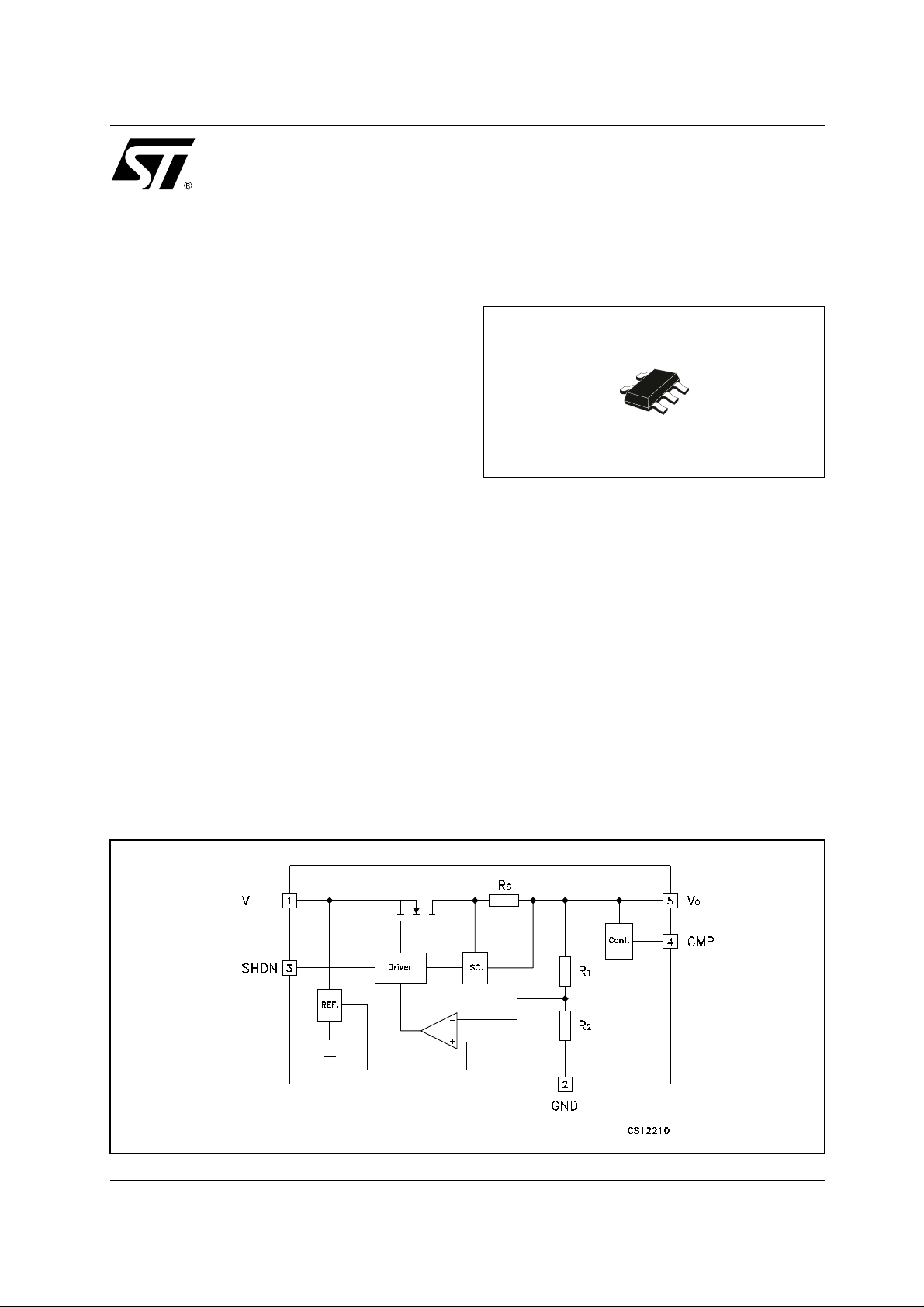
TSOT23-5L
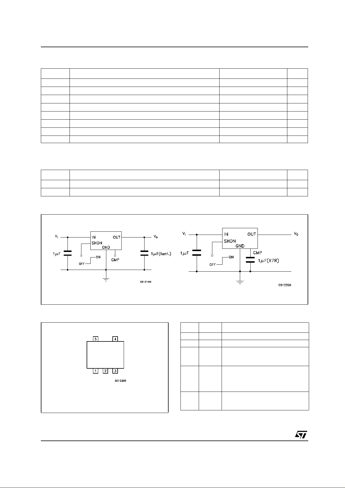
SCHEMATIC DIAGRAM
1/8April 2003
STC2G15
ABSOLUTE MAXIMUM RATINGS
Symbol Parameter Value Unit
V
V
V
INH
I
P
T
T
ESD Electrostatic Discharge HBM (DH11C) 2 kV
Absolute Maximum Ratings are those values beyond which damage to the device may occur. Functional operation under these condition is
not implied.
THERMAL DATA
Symbol Parameter TSOT23-5L Unit
R
thj-amb
R
thj-case
APPLICATION CIRCUITS
DC Input Voltage
I
DC Output Voltage -0.3 to VIN+0.3
O
INHIBIT Input Voltage -0.3 to VIN+0.3
Output Current
O
Power Dissipation
tot
Storage Temperature Range
stg
Operating Junction Temperature Range
op
Thermal Resistance Junction-ambient
Thermal Resistance Junction-case
-0.3 to 5.4 V
V
V
Internally limited
Internally limited
-55 to +150 °C
-40 to +95 °C
225 °C/W
81 °C/W
CONNECTION DIAGRAM (top view) PIN DESCRIPTION
Pin N° Symbol Name and Function
1 IN Input Pin
2 GND Ground Pin
3 SHDN Shutdown Input: Disables the
regulator when < 0.4V.Not internally
pulled down.
4 CMP Compensation Pin: Bypass with a
1µF ceramic X7R capacitor to GND
or leave floating if the C
connected to OUT pin
5 OUT Output Pin: Bypass with a 1µF
tantalium capacitor to GND if ceramic
X7R capacitoror is not used.
2/8
is
O
ORDERING CODES
TYPE TSOT23-5L OUTPUT VOLTAGES
STC2G15 STC2G15R 1.5V
STC2G15
ELECTRICAL CHARACTERISTICS (C
GND pin) or C
=1µF (ceramic X7R connected between CMP pin and GND pin) (unless otherwise
CMP
=1µF, CO=1µF (tantalium conn ected between OUT pin and
I
specified)
Symbol Parameter Test Conditions Min. Typ. Max. Unit
Input Voltage 2.7 5.2 V
V
I
V
Output Voltage VI= 2.7 to 5.2V IO= 0 to 15mA
O
T
= -40 to 95°C
J
t
Output Voltage Ramp-Up
RU
Time (Note 1)
Output VoltageRamp-Down
t
RD
Time (Note 2)
I
Current Capability 15 mA
O
Minimum Load Current
I
min
(Note 3)
IO= 0 to 15mA 10 15 µs
IO= 0 to 15mA 10 15 µs
Load Regulation (Note 4) 350 µV/mA
Temperature Drift (Note 4) 100 µV/K
SVR Supply Voltage Rejection
f = 1KHz 30 dB
(Note 5)
I
d
I
d
I
SHDN
V
SHDN
V
SHDN
Quiescent Current (ON
mode)
Quiescent Current (OFF
mode)
Shutdown Pin Current 2 4 µA
Shutdown Logic Enable
Low
Shutdown Logic Disabled
High
IO=0 30 µA
=0 VI= 2.7 to 5.2V 60 µA
I
O
Line Transient Response
Time (Notes 9, 13)
Load Transient Response
Time (Notes 10, 13)
Line Transient Response
Peak + (Notes 9)
Line Transient Response
Peak - (Notes 10)
Load Transient Response
Peak (Notes 11)
eN Output Noise Voltage B= 1kHz to 1MHz C
Note 1:Time for the output Voltage to rise from 50% to 85% of nominal value.
Note 2:Time for the output Voltage to fall from 85% to 50 of nominal value.
Note 3:Regulator must be able to sustain Regulated Output Voltage without load.
Note 4:Parameters are uncritical as long as the output voltage stays within limits.
Note 5:A sudden voltage rise/drop of 500mV mustn't bring the output Voltage out of limits.
Note 6:Ceramic Capacitors can be used if connected between CMP pin and GNG, instead of V
Note 8:Maximum and minimum values are guaranteed in full temperature range.
Note 9:Line transient is tested when the input voltage changes from 2.7 to 3.2V in 10µs in full load range.
Note 10: Line transient is tested when the input voltage changes from 3.2 to 2.7V in 10µs in full load range.
Note 11: Load transient is tested when the load changes from 0.1 to 15mA in 10µs in all the input range
Note 13: Response time is defined as the time form the load line step until the output reaches a value within specification (1.41V, 1.59V).
Note 14: The maximum power dissipation for the operation depends on the ambient temperature.
=95°C, TA=85°C and R
For T
J
increased by 4.5mW each degree below T
=220°C/W the maximum power can be 0.045W. The maximum power dissipation for operation can be
TJA
=85°C, and it must be derated by 4.5mW for each degree above 85°C
A
=1µF10mV
O
1.41 1.5 1.59 V
0mA
24µA
0.4 V
1.15 V
40 µs
50 µs
80 mV
60 mV
50 mV
pin and GND.
OUT
3/8

STC2G15
TYPICAL PE RFORMANCE CHARACTERISTICS (unless otherwise specified CIN=C
C
= Tant., Tj= 25°C)
OUT
Figure1 : O ut put Voltage vs Temperature
Figure2 : O ut put Voltage vs Temperature
Figure4 : O ut put Voltage vs Temperature
Figure5 : L ine Regulation vs Temperature
COMP
=SMDX5R
Figure3 : O ut put Voltage vs Temperature
4/8
Figure6 : L oad Regulation vs Tem perature

STC2G15
V
I
C
FSMD X7R,C
)
V
I
C
FSMD X7R,C
Figure7 : Inhibit Threshold Voltage vs
Temperature
Figure8 : Q uiescent Current vs Temperature
Figure10 : Supply Voltag e Rejection vs Output
Current
Figure11 : Dynamic Precharge Mode
Figure9 : Supply Voltage Rejection vs
Temperature
=5V,
I
=0.1to15mA,
O
I
=1µ
=2.2µF(tant
O
Figure12 : Dynamic Precharge Mode
=2.7 to3.7V,
I
t=1ms
=15mA,
O
I
=1µ
O
=2.2µF(tant),
5/8

STC2G15
V
C
FSMD X7R,C
)
V
I
C
FSMD X7R,C
F(tant)
V
I
C
FSMD X7R,C
)
Figure13 : Dynamic Precharge Mode
=0to2V,Noload,
INH
=1µ
I
=2.2µF(tant
O
Figure14 : Dynamic Precharge Mode
Figure15 : Dynamic Precharge Mode
=0to2V,
INH
=15mA,
O
I
=1µ
=1µF(tant
O
INH
6/8
=0to2V,
=15mA,
O
I
=1µ
=2.2µ
O

STC2G15
TSOT23-5L MECHANICAL D ATA
mm. mils
DIM.
MIN. TYP MAX. MIN. TYP. MAX.
A 1.1 43.3
A1 0 0.1 3.9
A2 0.7 1.0 27.6 39.4
b 0.3 0.5 11.8 19.7
C 0.08 0.2 3.1 7.9
D 2.9 114.2
E 2.8 110.2
E1 1.6 63.0
e0.95 37.4
e1 1.9 74.8
L 0.3 0.6 11.8 23.6
7282780/A
7/8

STC2G15
Information furnished is believed to be accurate and reliable. However, STMicroelectronics assumes no responsibility for the
consequences of use o f suc h inf ormat ion n or f or an y infr ingeme nt of paten ts or oth er ri gh ts of third part ies whic h may resul t f rom
its use. No license is granted by implication or otherwise under any patent or patent rights of STMicroelectronics. Specifications
mentioned in this publication are subject to change without notice. This publication supersedes and replaces all information
previously supplied. STMicroelectronics products are not authorized for use as critical components in life support devices or
systems without express written approval of STMicroelectronics.
Australia - Brazil - Canada - China - Finland - France - Germany - Hong Kong - India - Israel - Italy - Japan - Malaysia - Malta - Morocco
© The ST logo is a registered trademark of STMicroelectronics
© 2003 STMicroelectronics - Printed in Italy - All Rights Reserved
STMicroelectronics GROUP OF COMPANIES
Singapore - Spain - Sweden - Switzerland - United Kingdom - United States.
© http://www.st.com
8/8
 Loading...