

SGS Thomson Microelectronics M48Z58Y-70PC1, M48Z58Y, M48Z58-70PC1, M48Z58 Datasheet
64 Kbit (8Kb x 8) ZEROPOWER® SRAM
INTEGRATED ULTRA LOW POWER SRAM,
POWER-FAIL CONTROL CIRCUIT and
BATTERY
READ CYCLE TIME EQUALS WRITE CYCLE
TIME
AUTOMATIC P OWER-F AIL CHIP DES ELECT and
WRITE PROTECTION
WRITE PROTECT VOLT AGES
= Power-fail Deselect Voltage):
(V
PFD
– M48Z58: 4.50V ≤ V
– M48Z58Y: 4.20V ≤ V
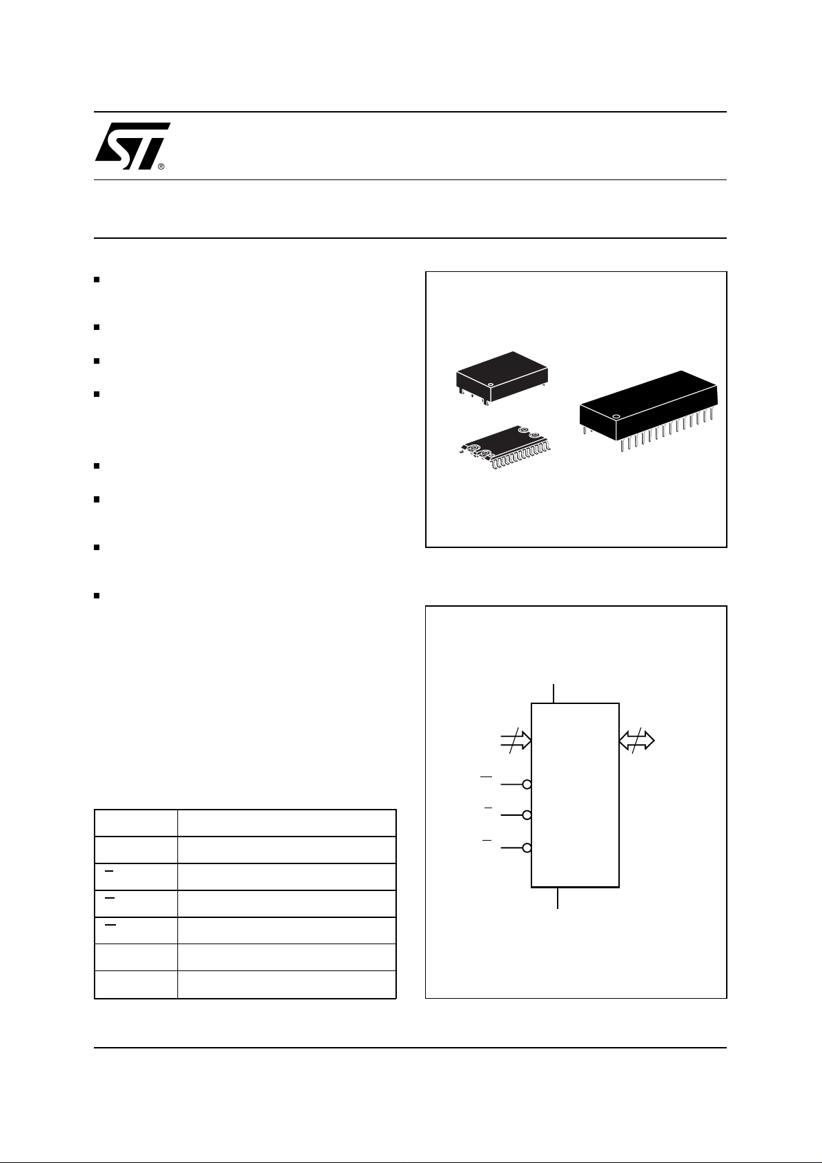
SELF-CONTAINED BATTERY in the CAPHAT
DIP PACKAGE
PACKAGING INCLUDES a 28-LEAD SOIC
and SNAPHAT
®
TOP
(to be Ordered Separately)
SOIC PACKAGE PROVIDES DIRECT
CONNECTION for a SNAPHAT TOP which
CONTAINS the BATTERY and CRYSTAL
PIN and FUNCTION COMPATIBLE with
JEDEC STANDARD 8K x 8 SRAMs
PFD
PFD
4.75V
≤
≤
4.50V
SNAPHAT (SH)
Battery
28
28
1
SOH28 (MH)
Figure 1. Logic Diagram
M48Z58
M48Z58Y
1
PCDIP28 (PC)
Battery CAPHAT
DESCRIPTION
The M48Z58/58Y ZEROPOW ER
®
RAM is an 8K x
V
CC
8 non-volatile static RAM that integrates power-fail
deselect circuitry and battery control logic on a
single die. The monolithic chip is available in two
special packages to provide a highly integrated
A0-A12
13
8
DQ0-DQ7
battery backed-up memory solution.
T ab le 1. Signal Names
W
A0-A12 Address Inputs
DQ0-DQ7 Data Inputs / Outputs
E Chip Enable
G Output Enable
W Write Enable
V
CC
V
SS
March 1999 1/17
Supply Voltage
Ground
E
G
M48Z58
M48Z58Y
V
SS
AI01176B
M48Z58, M48Z58Y
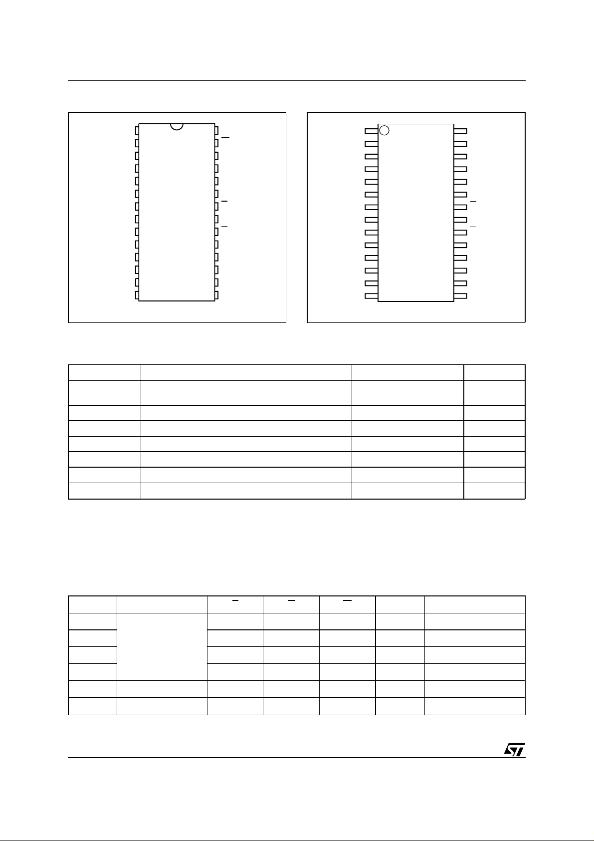
Figure 2A. DIP Pin Connections
28
27
26
25
24
23
22
21
20
19
18
17
16
15
AI01177B
CC
W
NC
A8
A9
A11
G
A10
E
DQ7
DQ6
DQ5DQ1
DQ4
DQ3V
Warning:
NC V
1
A12
2
3
A7
4
A6
5
A5
6
A4
7
A3
A2
A1
A0
DQ0
8
9
10
11
M48Z58
M48Z58Y
12
13
DQ2
14
SS
NC = Not Connected.
T ab le 2. Absolute Maximum Ratings
(1)
Figure 2B. SOIC Pin Connections
Warning:
NC V
A12
A7
A6
A5
A4
A3
A2
A1
A0
DQ0
1
2
3
4
5
6
7
M48Z58Y
8
9
10
11
12
DQ2
SS
13
14
NC = Not Connected.
28
27
26
25
24
23
22
21
20
19
18
17
16
15
AI01178B
Symbol Parameter Value Unit
T
A
T
STG
(2)
T
SLD
V
IO
V
CC
I
O
P
D
Notes:
1. Stresses greater than those listed under "Absolute Maximum Ratings" may cause permanent damage to the device. This is a
stress rating only and functional operation of the device at these or any other conditions above those indi cat ed in the operati onal
section of this specification is not implied. Exposure to the absolute maximum rating conditions for extended periods of time may
affect reliability.
2. Soldering temperature not to exceed 260°C for 10 seconds (total thermal budget not to exceed 150°C for longer than 30 seconds).
CAUTION: Negat i ve undershoots below –0.3 volts are not allowed on any pin while in the Battery Back-up mode.
CAUTION: Do NOT wave solder SOIC to avoid damaging SNAPHAT sockets.
Ambient Operating Temperature Grade 1
Grade 6
Storage T emper ature (VCC Off) –40 to 85 °C
Lead Solder Temperature for 10 seconds 260 °C
Input or Output Voltages –0.3 to 7 V
Supply Voltage –0.3 to 7 V
Output Current 20 mA
Power Dissipation 1 W
0 to 70
–40 to 85
CC
W
NC
A8
A9
A11
G
A10
E
DQ7
DQ6
DQ5DQ1
DQ4
DQ3V
°C
T ab le 3. Operating Modes
Mode V
CC
(1)
Deselect
Write V
Read V
4.75V to 5.5V
or
4.5V to 5.5V
Read V
Deselect V
SO
to V
Deselect ≤ V
Notes
: 1. X = V
2. See Table 7 for details.
or VIL; VSO = Battery Back-up Switchover Voltage.
IH
PFD
(min)
SO
(2)
2/17
E G W DQ0-DQ7 Power
V
IH
IL
IL
IL
X X High Z Standby
XVILD
V
IL
V
IH
V
IH
V
IH
IN
D
OUT
High Z Active
Active
Active
X X X High Z CMOS Standby
X X X High Z Battery Back-up Mode
Figure 3. Block Diagram
M48Z58, M48Z58 Y
A0-A12
LITHIUM
CELL
VOLTAGE SENSE
AND
SWITCHING
CIRCUITRY
V
CC
DESCRIPTION
(cont’d)
The M48Z58/58Y is a non-volatile pin and function
equivalent to any JEDEC standard 8K x 8 SRAM.
It also easily fits into many ROM, EPROM, and
EEPROM sockets, providing the non-volatility of
PROMs without any requirement for special write
timing or limitations on the number of writes t hat
can be performed.
The 28 pin 600mil DIP CAPHAT houses the
M48Z58/58Y silicon with a long life lithium button
cell in a single package.
The 28 pin 330mil SOIC provides s ockets with gold
plated contacts at both ends for direct connection
to a separate SNAPHAT housing containing the
battery. The unique design allows the SNAPHAT
battery package to be mounted on top of the SOIC
package after the completion of the surface mount
process. Insertion of the SNAPHAT housing after
reflow prevents potential battery damage due to the
high temperatures required for device surfacemounting. The SNAPHAT housing is keyed to prevent reverse insertion.
The SOIC and battery packages are shipped separately in plastic anti-static tubes or in Tape & Reel
form.
POWER
V
PFD
8K x 8
SRAM ARRAY
V
SS
Table 4. AC Measurement Conditions
Input Rise and Fall Times ≤ 5ns
Input Pulse Voltages 0 to 3V
Input and Output Timing Ref. Voltages 1.5V
Note that Output Hi-Z is defined as the point where data is no
longer driven.
Figure 4. AC Testing Load Circuit
5V
1.9kΩ
DEVICE
UNDER
TEST
1kΩ
CL includes JIG capacitance
CL = 100pF or 5pF
DQ0-DQ7
E
W
G
AI01394
OUT
AI01030
3/17
M48Z58, M48Z58Y
(1, 2)
T ab le 5. Capacitance
= 25 °C)
(T
A
Symbol Parameter T est Condition Min Max Unit
C
IN
(3)
C
IO
Notes:
1. Effective capacitance measured with power supply at 5V .
2. Sampled only, not 100% tested.
3. Outputs deselected.
Input Capacitance VIN = 0V 10 pF
Input / Output Capacitance V
= 0V 10 pF
OUT
T ab le 6. DC Characteristics
= 0 to 70°C or –40 to 85°C; VCC = 4.75V to 5.5V or 4.5V to 5.5V)
(T
A
Symbol Parameter Test Condition Min Max Unit
I
LI
I
LO
Supply Current Outputs open 50 mA
I
CC
I
CC1
I
CC2
V
IL
V
IH
V
OL
V
OH
T able 7. Power Down/Up Trip Points DC Characteristics
= 0 to 70°C or –40 to 85°C)
(T
A
Input Leakage Current 0V ≤ VIN ≤ V
Output Leakage Current 0V ≤ V
Supply Current (Standby) TTL E = V
Supply Current (Standby) CMOS E = VCC – 0.2V 3 mA
OUT
≤ V
IH
CC
CC
±1 µA
±5 µA
3mA
Input Low Voltage –0.3 0.8 V
Input High Voltage 2.2 VCC + 0.3 V
Output Low Voltage IOL = 2.1mA 0.4 V
Output High Voltage IOH = –1mA 2.4 V
(1)
Symbol Parameter Min Typ Max Unit
V
PFD
V
PFD
Power-fail Deselect Voltage (M48Z58/58Y) 4.5 4.6 4.75 V
Power-fail Deselect Voltage (M48Z58/58YY) 4.2 4.35 4.5 V
V
SO
t
DR
Notes:
1. All voltages referenced to V
2. At 25 °C
DESCRIPTION
Battery Back-up Switchover Voltage 3.0 V
(2)
Expected Data Retention Time 10 YEARS
.
SS
(cont’d)
For the 28 lead SOIC, the battery package (i.e.
SNAPHAT) part number is "M4Z28-BR00SH1".
The M48Z58/58Y also has its own Power-fail Detect circuit. The control circuitry constantly monitors
the single 5V supply for an out of tolerance condi-
4/17
tion. When V
is out of tolerance, the circuit write
CC
protects the SRAM, providing a high degree of data
security in the midst of unpredictable system operation brought on by low V
. As VCC falls below
CC
approximately 3V , the control circuitry connects the
battery which maintains data until valid power returns.
M48Z58, M48Z58 Y
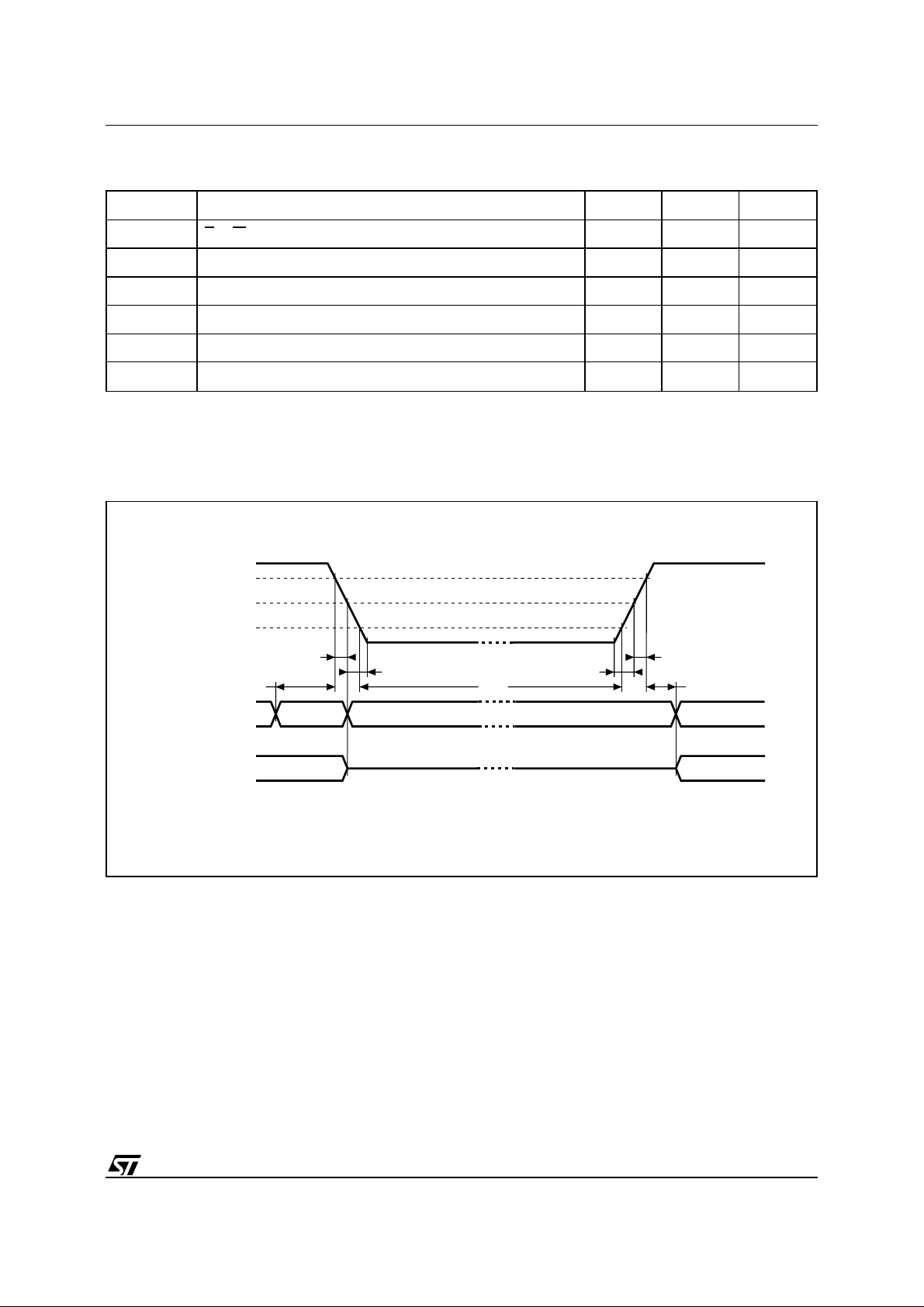
T able 8. Power Down/Up Mode AC Characteristics
= 0 to 70°C or –40 to 85°C)
(T
A
Symbol Parameter Min Max Unit
E or W at VIH before Power Down 0 µs
V
(max) to V
PFD
V
(min) to VSS VCC Fall Time 10 µs
PFD
V
(min) to V
PFD
VSS to V
V
(max) to V
PFD
passes V
CC
(min) to VSS fall time of less than tFB may cause corruption of RAM data.
PFD
(min) = 20ms for industrial temperature grade 6 device.
REC
PFD
(max) to Inputs Recognized 40 200 ms
PFD
(min) fall time of less than tF may result in deselection/writ e protection not occ urri ng until 200 µs after
PFD
(min).
PFD
(min) VCC Fall Time 300 µs
PFD
(max) VCC Rise Time 10 µs
PFD
(min) VCC Rise Time 1 µs
Notes
t
t
F
t
FB
t
t
REC
:1.V
2. V
3. t
PD
(1)
(2)
t
R
RB
(3)
V
Figure 5. Power Down/Up Mode AC Waveforms
V
CC
V
(max)
PFD
V
(min)
PFD
VSO
INPUTS
OUTPUTS
tF
tPD
tFB
tDR
tRB
DON'T CARE
VALID VALID
(PER CONTROL INPUT)
HIGH-Z
tR
tREC
RECOGNIZEDRECOGNIZED
(PER CONTROL INPUT)
AI01168C
5/17
M48Z58, M48Z58Y
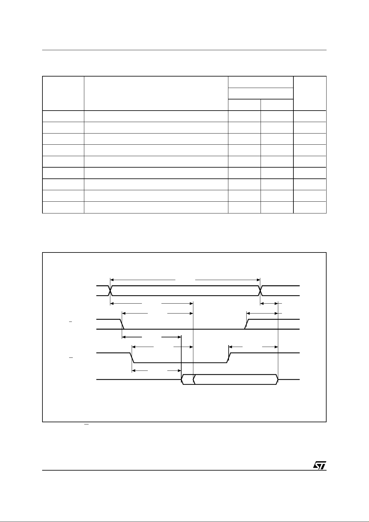
T ab le 9. Read Mode AC Characteristics
= 0 to 70°C or –40 to 85°C; VCC = 4.75V to 5.5V or 4.5V to 5.5V)
(T
A
Symbol Parameter
Notes:
t
AVAV
(1)
t
AVQV
(1)
t
ELQV
(1)
t
GLQV
(2)
t
ELQX
(2)
t
GLQX
(2)
t
EHQZ
(2)
t
GHQZ
(1)
t
AXQX
1. C
= 100pF (see Figure 4).
L
= 5pF (see Figure 4).
2. C
L
Read Cycle Time 70 ns
Address Valid to Output Valid 70 ns
Chip Enable Low to Output Valid 70 ns
Output Enable Low to Output Valid 35 ns
Chip Enable Low to Output Transition 5 ns
Output Enable Low to Output Transition 5 ns
Chip Enable High to Output Hi-Z 25 ns
Output Enable High to Output Hi-Z 25 ns
Address Transition to Output Transitio n 10 ns
M48Z58 / M48Z58Y
-70
Min Max
Unit
Figure 6. Read Mode AC Waveforms
A0-A12
E
G
DQ0-DQ7
Note:
Write Enable (
W) = High.
tAVAV
VALID
tAVQV tAXQX
tELQV
tELQX
tGLQX
tGLQV
tGHQZ
VALID
tEHQZ
AI01385
6/17
 Loading...