

SGS Thomson Microelectronics M48Z2M1Y-70PL1, M48Z2M1Y, M48Z2M1-70PL1, M48Z2M1 Datasheet
16 Mb (2Mb x 8) ZEROPOWER® SRAM
INTEGRATED LOW POWER SRAM,
POWE R-FAIL CONT ROL CIRCUIT and
BATTERIES
CONVENTIONA L SRAM OPERATION;
UNLIMITED W RI TE CYCLE S
10 YEARS of DATA RETENTION in the
ABSENCE of POWER
AUTOMATIC POWER-FAIL CHIP DESELECT
and WRITE PROTECTION
WRITE PROTECT VOLTAGES
= Power-fail Deselect Voltage):
(V
PFD
– M48Z2M1: 4.5V ≤ V
– M48Z2M1Y: 4.2V ≤ V
BA T TERIES A RE INTERNALLY ISOLATED
UNTIL POWER IS APPLIED
PIN and FUNCTION COMPATIBLE with
JEDEC STANDARD 2Mb x 8 SRAMs
PFD
PFD
≤ 4.75V
≤ 4.50V
M48Z2M1
M48Z2M1Y
36
1
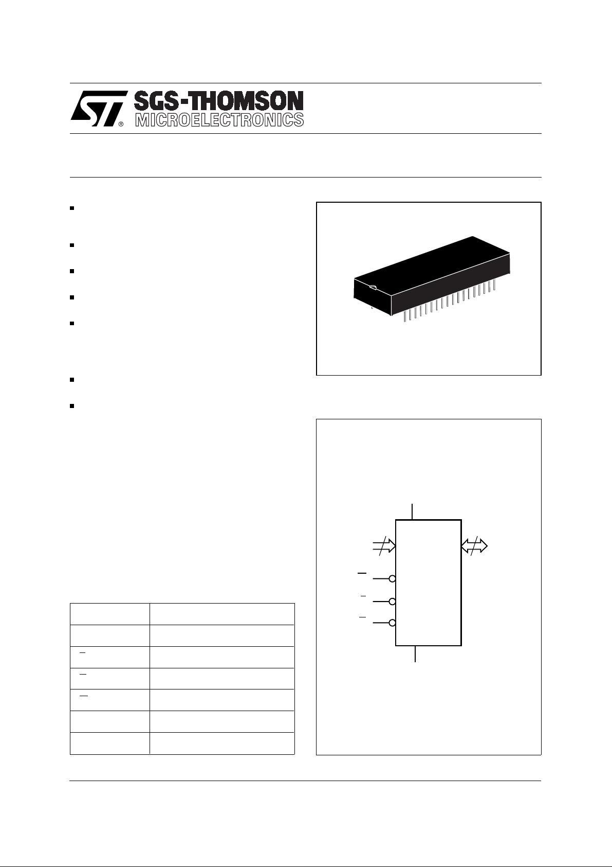
PMLDIP36 (PL)
Module
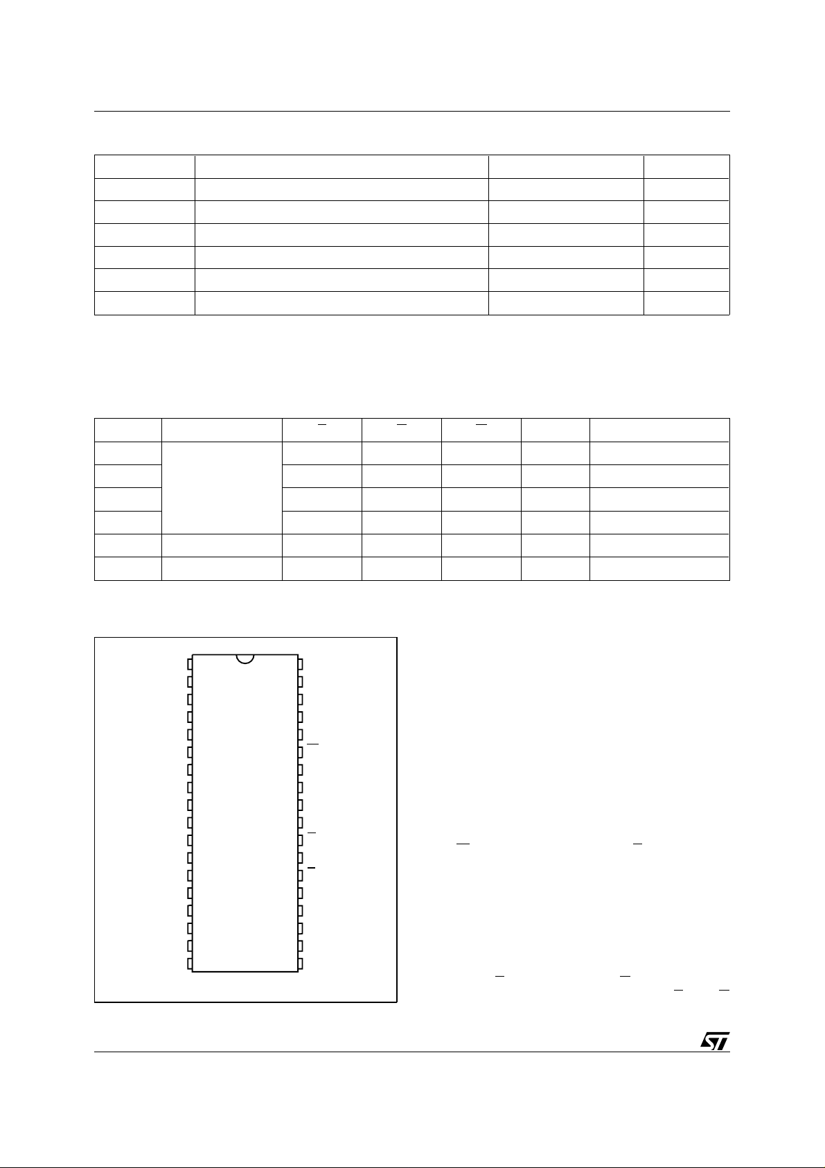
Figure 1. Logic Diag ra m
DESCRIP TION
®
The M48Z2M1/2M1Y ZEROPOWER
RAM is a
non-volatile 16,777,216 bit Static RAM organized
as 2,097,152 words by 8 bits. The device combines
two internal lithium bat teries, CMO S SRA Ms and a
control circuit in a plastic 36 pin DIP long Module.
The ZEROPOWER RAM replaces industry standard SRAM s. It provides the nonvolatility of P ROMs
without any requirement for special write timing or
limitations on the number of writes that can be
performed.
T able 1. Signal Names
A0-A20 Address Inputs
DQ0-DQ7 Data Inputs / Outputs
E Chip Enable
G Output Enable
W Write Enable
V
CC
V
SS
Supply Voltage
Ground
A0-A20
W
V
CC
21
M48Z2M1
M48Z2M1Y
E
G
V
SS
8
DQ0-DQ7
AI02048
January 1998 1/12
This is preliminary information on a new product now in development or undergoing evaluation. Details are subject to change without notice.
M48Z2M1 , M48Z2M1Y
T ab le 2. Absolut e Maximu m Ra t ings
Symbol Parameter Value Unit
T
A
T
STG
T
BIAS
(2)
T
SLD
V
IO
V
CC
Notes: 1. Stresses greater than those listed under "Absolute Maximum Ratings" may cause permanent damage to the device. This is a
stress rating only and functional operation of the device at these or any other conditions above those indicated in the operational
section of this specification is not implied. Exposure to the absolute maximum rating conditions for extended periods of time may
affect reliability.
2. Soldering temperature not to exceed 260°C for 10 seconds (total thermal budget not to exceed 150°C for longer than 30 seconds).
CAUTION: Negative undershoots below –0.3 volts are not allowed on any pin while in the Battery Back-up mode.
Ambient Operating Temperature 0 to 70 °C
Storage Temperature (VCC Off) –40 to 85 °C
Temperature Under Bias –40 to 85 °C
Lead Soldering Temperature for 10 seconds 260 °C
Input or Output Voltages –0.3 to 7 V
Supply Voltage –0.3 to 7 V
(1)
T ab le 3. Operating Modes
Mode V
Deselect
Write V
Read V
Read V
Deselect V
Deselect ≤ V
Notes: X = VIH or VIL; VSO = Battery Back-up Swit chover V olt age.
CC
4.75V to 5.5V
or
4.5V to 5.5V
to V
SO
(min) X X X High Z CMOS Standby
PFD
SO
E G W DQ0-DQ7 Power
V
IH
IL
IL
IL
X X X High Z Battery Back-up Mode
X X High Z Standby
XVILD
V
IL
V
IH
V
IH
V
IH
IN
D
OUT
High Z Active
Active
Active
Figure 2. DIP Pin Connection s
1
NC
2
A20
A18
3
A16
4
5
A14
6
A12
A7
7
A6
8
A5
A4
A3
A2
A1
A0
DQ0
M48Z2M1
9
M48Z2M1Y
10
11
12
13
14
15
16
DQ2
17
18
V
SS
Warning: NC = Not Connected.
36
35
34
33
32
31
30
29
28
27
26
25
24
23
22
21
20
19
AI02049
V
CC
A19
NC
A15
A17
W
A13
A8
A9
A11
G
A10
E
DQ7
DQ6
DQ5DQ1
DQ4
DQ3
DESCRIPTION (c ont’d)
The M48Z2M1/2M 1Y has its own Power-fail Detect
Circuit. The cont rol circuitry c onstantly monitors the
single 5V supply for an out of tolerance condition.
When V
is out of tolerance, the circuit write
CC
protects the SRAM, providing a high degree of data
security in the midst of unpredictable system operations brought on by low V
. As VCC falls below
CC
approximately 3V , the control circuitry connects the
batteries which sustain data until valid power returns.
READ MODE
The M48Z2M1/2M1Y is in the Read Mode when -
W (Write Enable) is high and E (Chip E nable)
ever
is low. The device architecture allows ripplethrough access of data from eight of 16,777,216
locations in the static storage array. Thus, the
unique address specified by the 21 Address Inputs
defines which one of the 2,097,152 bytes of data is
to be accessed. Valid data will be available at the
Data I/O pins within Address Access time (t
AVQV
after the last a ddress input signal is stable, provi ding that the
access times are also satisfied. If the
E (Chip Enable) and G (Output Enable)
E and G
access times are not met, valid data will be avail-
)
2/12
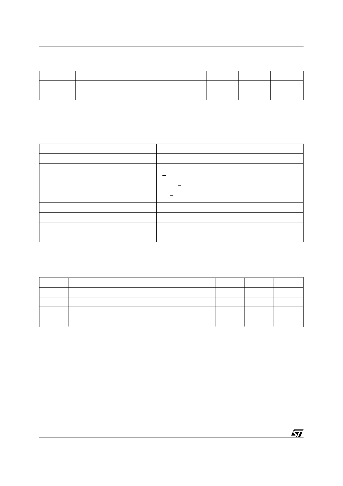
Figure 3. Block Diagram
M48Z2M1, M48Z 2M1 Y
V
CC
A0-A20
POWER
VOLTAGE SENSE
E
AND
SWITCHING
CIRCUITRY
INTERNAL
BATTERIES
able after the later of Chip Enable Access time
) or Output Enable Access Time (t
(t
ELQV
GLQV
). Th e
state of the eight three-state Data I/O signals is
controlled by
before t
indeterminate state until t
puts are changed while
E and G. If the outputs are activated
, the data lines will be driven to an
AVQ V
. If the Address In-
AVQV
E and G remain low, output
data will remain valid for Output Data Hold time
(t
) but will go indeterminate until the next Ad-
AXQX
dress Acc ess.
2048K x 8
SRAM ARRAY
E
V
SS
DQ0-DQ7
W
G
AI02050
Tab le 4. AC Measurement Con ditio ns
Input Rise and Fall Times ≤ 5ns
Input Pulse Voltages 0 to 3V
Input and Output Timing Ref. Voltages 1.5V
Note that Output Hi-Z is defined as the point where data is no
longer driven.
Figure 4. AC T esti ng Load Circui t
WRIT E MO D E
The M48Z2M1/2M1Y is in the Write Mode when-
W and E are active. The start of a write is
ever
referenced from the latter occur ring falling edge of
W or E. A write is terminated by the earlier rising
edge of
W or E.
The addresses must be held valid throughout the
cycle.
E or W must retur n high for minimum of t
from E or t
from W prior to the initiation of
WHAX
EHAX
another read or write cycle. Data-in must be valid
or t
t
DVEH
valid for t
prior to the end of write and remain
DVWH
EHDX
or t
afterward. G should be kept
WHDX
high during write cycles to avoid bus contention;
although, if the output bus has been activated by a
low on
t
E and G, a low on W will disable the outputs
after W falls.
WLQZ
DEVICE
UNDER
TEST
1kΩ
CL includes JIG capacitance
5V
1.9kΩ
OUT
CL = 100pF or 5pF
AI01030
3/12
M48Z2M1 , M48Z2M1Y
T ab le 5. Capacitance
= 25 °C, f = 1 MHz )
(T
A
(1, 2)
Symbol Parameter Test Condition Min Max Unit
C
IN
(3)
C
IO
Notes: 1. Effective capacitance measured with power supply at 5V.
2. Sampled only , not 100% teste d.
3. Outputs deselected
Input Capacitance VIN = 0V 40 pF
Input / Output Capacitance V
= 0V 40 pF
OUT
T ab le 6. DC Characteristics
= 0 to 70°C; VCC = 4.75V to 5.5V or 4.5V to 5.5V)
(T
A
Symbol Parameter Test Condition Min Max Unit
(1)
I
LI
(1)
I
LO
I
Supply Current E = VIL, Outputs open 140 mA
CC
I
CC1
I
CC2
V
IL
V
IH
V
OL
V
OH
Note: 1. Outputs deselected.
Input Leakage Current 0V ≤ VIN ≤ V
Output Leakage Current 0V ≤ V
OUT
≤ V
CC
CC
±4 µA
±4 µA
Supply Current (Standby) TTL E = VIH 10 mA
Supply Current (Standby) CMOS E ≥ VCC – 0.2V 8 mA
Input Low Voltage –0.3 0.8 V
Input High Voltage 2.2 VCC + 0.3 V
Output Low Voltage IOL = 2.1mA 0.4 V
Output High Voltage IOH = –1mA 2.4 V
T ab le 7. Power Down/Up T ri p Points DC Characteri stics
= 0 to 70°C)
(T
A
(1)
Symbol Parameter Min Typ Max Unit
V
PFD
V
PFD
V
SO
t
DR
Notes: 1. All voltages referenced to VSS.
2. At 25°C
Power-fail Deselect Voltage (M48Z2M1) 4.5 4.6 4.75 V
Power-fail Deselect Voltage (M48Z2M1Y) 4.2 4.3 4.5 V
Battery Back-up Switchover Voltage 3 V
(2)
Data Retention Time 10 YEARS
4/12
 Loading...