

SGS Thomson Microelectronics LM2903N, LM2903D, LM2903 Datasheet
LOW POWERDUAL VOLTAGE COMPARATORS
.WIDESINGLESUPPLYVOLTAGE RANGEOR
DUAL SUPPLIES +2V TO +36V OR ±1V TO
±18V
.VERYLOWSUPPLYCURRENT(0.4mA)INDE-
PENDENT OF SUPPLYVOLTAGE
(1 mW/comparator at +5V)
.LOW INPUT BIAS CURRENT : 25nA TYP
.LOW INPUT OFFSET CURRENT : ±5nA TYP
.INPUT COMMON-MODE VOLTAGE RANGE
INCLUDESGROUND
.LOW OUTPUT SATURATION VOLTAGE :
250mV TYP. (IO= 4mA)
.DIFFERENTIAL INPUT VOLTAGE RANGE
EQUAL TO THE SUPPLY VOLTAGE
.TTL, DTL, ECL, MOS, CMOS COMPATIBLE
OUTPUTS
DESCRIPTION
This device consistsof two independent low power
voltagecomparators designed specifically to operate from a single supply over a wide range of voltages. Operation from split power supplies is also
possible.
These comparators also have a unique
characteris-tic in the fact that the input common-mode voltage range includes ground even
though operated from a single power supply voltage.
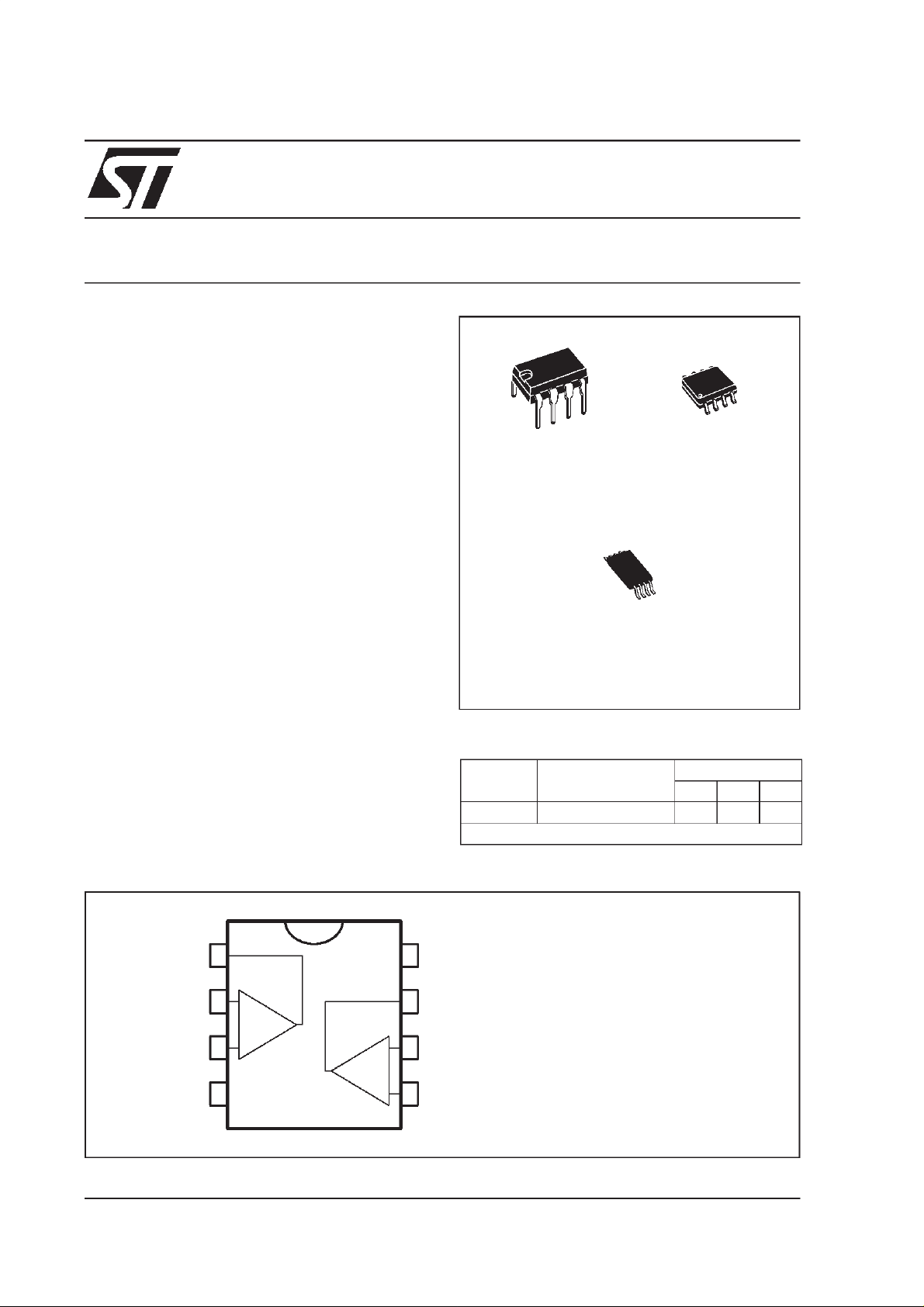
N
DIP8
(PlasticPackage)
(Thin ShrinkSmall Outline Package)
ORDER CODES
Part
Number
LM2903 -40, +125
Example : LM2903N
Temperature
Range
LM2903
(PlasticMicropackage)
P
TSSOP8
o
C
D
SO8
Package
NDP
•••
PIN CONNECTIONS (t op v ie w)
1
2
-
+
3
45
April 2000
8
1 - Output 1
7
-
+
6
2 - Inverting input 1
3 - Non-inverting input 1
-
4-V
CC
5 - Non-inverting input 2
6 - Inverting input 2
7 - Output 2
+
8-V
CC
1/10
LM2903
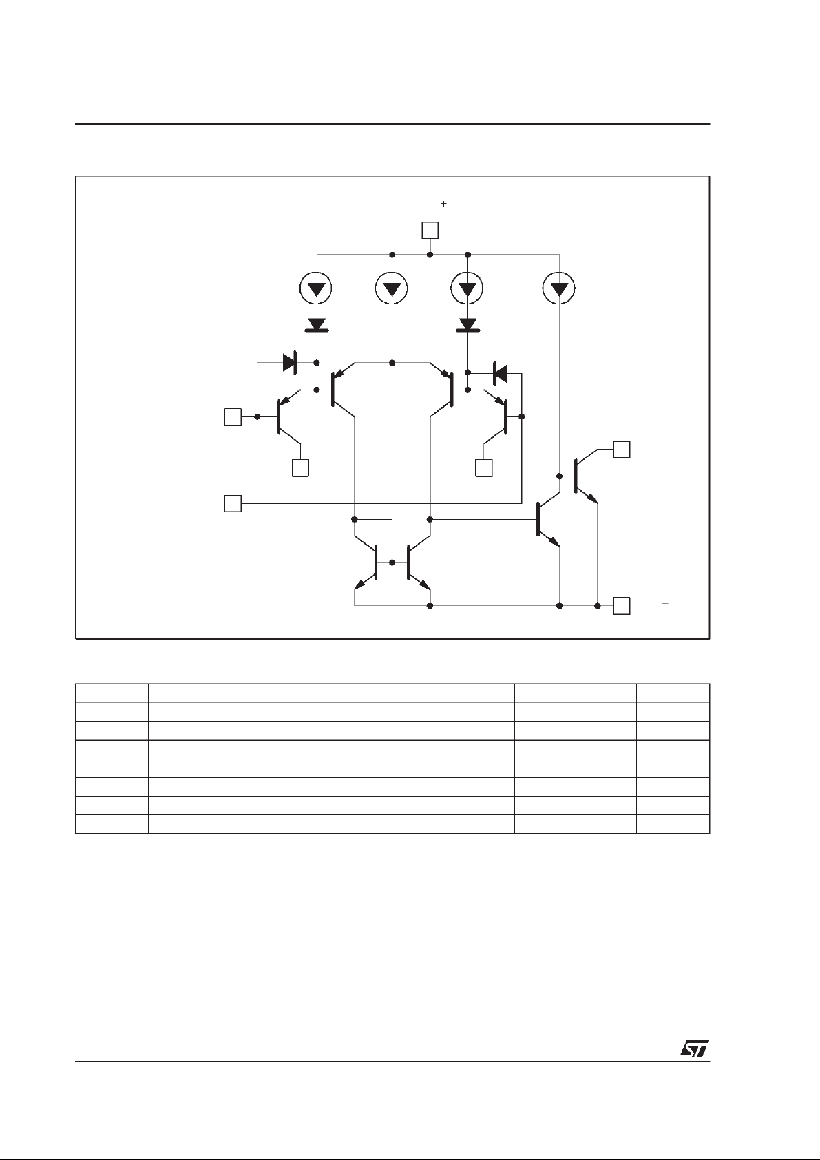
SCHEMATIC DIAGR AM (1/2 LM2903)
V
CC
3.5
µA
Non-inverting
Input
V
CC
Inverting
Input
ABSOLUTE MAXIMUM RATINGS
100
µA
V
3.5µA 100µA
CC
V
O
V
CC
Symbol Parameter Value Unit
V
CC
V
id
V
Supply Voltage
±18 or 36
Differential Input Voltage !36 V
Input Voltage -0.3 to +36 V
i
Output Short-circuit to Ground – (note 1) Infinite
P
tot
T
oper
T
stg
Notes : 1. Short-circuit f rom the output toV
Power Dissipation 830 mW
Operating Free-air TemperatureRange -40 to +125
Storage Temperature Range -65 to +150
+
can cause excessive heating and eventual destruction. The maximum output
current is approximately 20mA, i ndependent of the magnitude of V
CC
+
.
CC
2/10
V
o
C
o
C

LM2903
ELECTRICAL CHARACTERISTICS
+
V
= +5V, V
CC
Symbol Parameter Min. Typ. Max. Unit
V
io
I
ib
I
io
A
vd
I
CC
V
icm
V
id
I
sink
V
OL
I
OH
t
re
t
rel
Notes : 2.
3. The directi on of thei nput current is out of the IC duet o the PNP input stage. This current isessenti ally constant,
4. The input common-mode voltage of either inputs ignal voltage should not beal lowed to go negative bym ore than
5. The response t i me specified is for a 100mV input step with 5mV overdrive.
6. Po sit ive excurs io ns of i nput vol tag e may exceed the power s upply l evel.
7. Maximum values are guaranteed by design.
–
CC
= 0V, T
=25oC (unless otherwise specified)
amb
Input Offset Voltage – (note 2)
T
amb
T
min
= +25oC
. ≤ T
amb
≤ T
max.
17
15
Input Bias Current – (note 3)
T
amb
T
min
= +25oC
. ≤ T
amb
≤ T
max.
25 250
400
Input Offset Current
T
= +25oC
amb
. ≤ T
T
min
amb
≤ T
max.
Large Signal Voltage Gain
V
= 15V, RL= 15kΩ,Vo= 1 to 11V
CC
25 200
550
150
V/mV
Supply Current (all comparators)
V
= 5V, no load
CC
V
= 30V, no load
CC
Input Common Mode Voltage Range (VCC= 30V) - (note 4)
T
amb
T
min
= +25oC
. ≤ T
amb
≤ T
max.
0
0
Differential Input Voltage - (note 6) V
0.4
1
1
2.5
+
V
-1.5
CC
+
V
-2
CC
+
CC
Output Sink Current
(V
= -1V, VO= 1.5V) 6 16
id
Low Level Output Voltage
(V
T
T
amb
min
= -1V, I
id
=25oC
. ≤ T
amb
sink
≤ T
= 4mA)
max.
250 400
700
High Level Output Current
(V
= 1V, VCC=VO= 30V)
id
T
=25oC
amb
. ≤ T
T
min
Small Signal Response Time
(R
L
Large Signal Response Time - (note 7)
TTL Input (V
Output Signal at 50% of final value
≤ T
amb
max.
= 5.1kΩ to V
ref
+
) - (note 5)
CC
= +1.4 V, RL= 5.1kΩ to V
+
)
CC
Output Signal at 95% of final value
At output switch point, VO#1.4V,RS=0Ωwith V
+
toV
1.5V).
CC
independent of t he state of the output, so no l oading charge exi sts on the reference or input li nes.
0.3V. T he upper end of the common-mode voltage range is V
without damage.
As long asthe other voltage remains w ithin thec ommon-mode range thecomparator wil lprovide a proper output
state. Thelow i nput voltagestat e mustnot beles s than–0.3V (or0. 3V belowt henegative power supply, if used).
+
from 5Vto30V andoverthe full inputcommon-mode range (0V
CC
+
–1.5V, but either or both inputs can go to +30V
CC
0.1
1
1.3
500
1
mV
nA
nA
mA
V
V
mA
mV
nA
µA
µs
ns
µs
3/10
 Loading...