

®
FEATURES
HIGH SURGE CURRENT CAPABILITY
.
COMMUTATION : (dV/dt)c > 10V/µs
.
BTB24 B
STANDARD TRIACS
DESCRIPTION
The BTB24 B triac family are high performance
glass passivated PNPN devices.
These parts are suitables for general purpose applications where high surge current capability is required. Application such as phase control and
static switching on inductive or resistive load.
ABSOLUTE RATINGS
Symbol Parameter Value Unit
I
T(RMS)
I
TSM
I2tI
dI/dt Critical rate of rise of on-state current
Tstg
Tj
Tl Maximum lead temperature for soldering during 10 s at 4.5 mm
RMS on-state current
(360° conduction angle)
Non repetitive surge peak on-state current
( Tj initial = 25°C )
2
t value tp = 10 ms 312 A2s
Gate supply : IG = 2 . IGT tr ≤ 100ns
Storage and operating junction temperature range - 40 to + 150
from case
(limiting values)
Tc = 90 °C25 A
tp = 8.3 ms 260 A
tp = 10 ms 250
Repetitive
F = 100 Hz
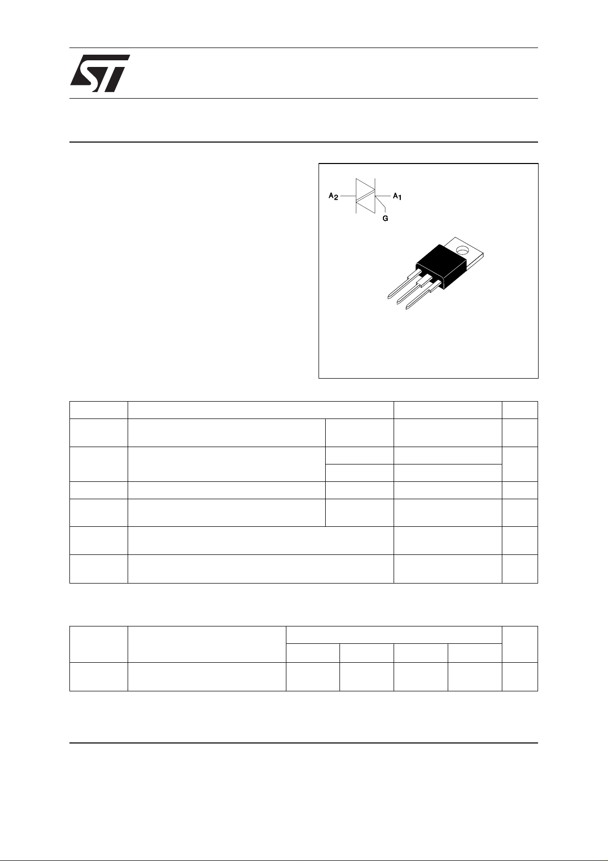
A1
A2
G
TO220AB
(Plastic)
50 A/µ s
- 40 to + 125
260 ° C
°C
°C
Symbol Parameter BTB24-... B Unit
400 600 700 800
V
DRM
V
RRM
October 1998 - Ed: 2A
Repetitive peak off-state voltage
Tj = 125 °C
400 600 700 800 V
1/4
BTB24 B
THERMAL RESISTANCES
Symbol Parameter Value Unit
Rth (j-a) Junction to ambient 60 °C/W
Rth (j-c) DC Junction to case for DC 1.5 °C/W
Rth (j-c) AC Junction to case for 360° conduction angle ( F= 50 Hz) 1.1 °C/W
GATE CHARACTERISTICS
P
= 1W PGM = 10W (tp = 20 µs) IGM = 4A (tp = 20 µs) VGM = 16V (tp = 20 µs).
G (AV)
(maximum v alu es )
ELECTRICAL CHARACTERISTICS
Symbol Test Conditions Quadrant Suffix Unit
I
GT
V
GT
V
GD
I
L
IH *I
VTM *ITM= 35A tp= 380µs Tj=25°C MAX 1.6 V
I
DRM
I
RRM
dV/dt * Linear slope up to VD=67%V
(dV/dt)c * (dI/dt)c = 11.1A/ms Tj=125°C MIN 10 V/µs
* For either polarit y of electrode A2 voltage with reference to elec trode A1.
VD=12V (DC) RL=33Ω Tj=25°C I-II-III-IV MIN 5 mA
I-II-III MAX 50
IV MAX 100
VD=12V (DC) RL=33Ω Tj=25°C I-II-III-IV MAX 1.3 V
VD=V
IG=1.2 I
RL=3.3kΩ Tj=125°C I-II-III-IV MIN 0.2 V
DRM
GT
Tj=25°C I-III-IV MAX 70 mA
II 150
= 500mA gate open Tj=25°C MAX 50 m A
T
V
DRM
V
RRM
Rated
Rated
DRM
Tj=25°CMAX5µA
Tj=125°CMAX2mA
Tj=125°C MIN 750 V/µs
gate open
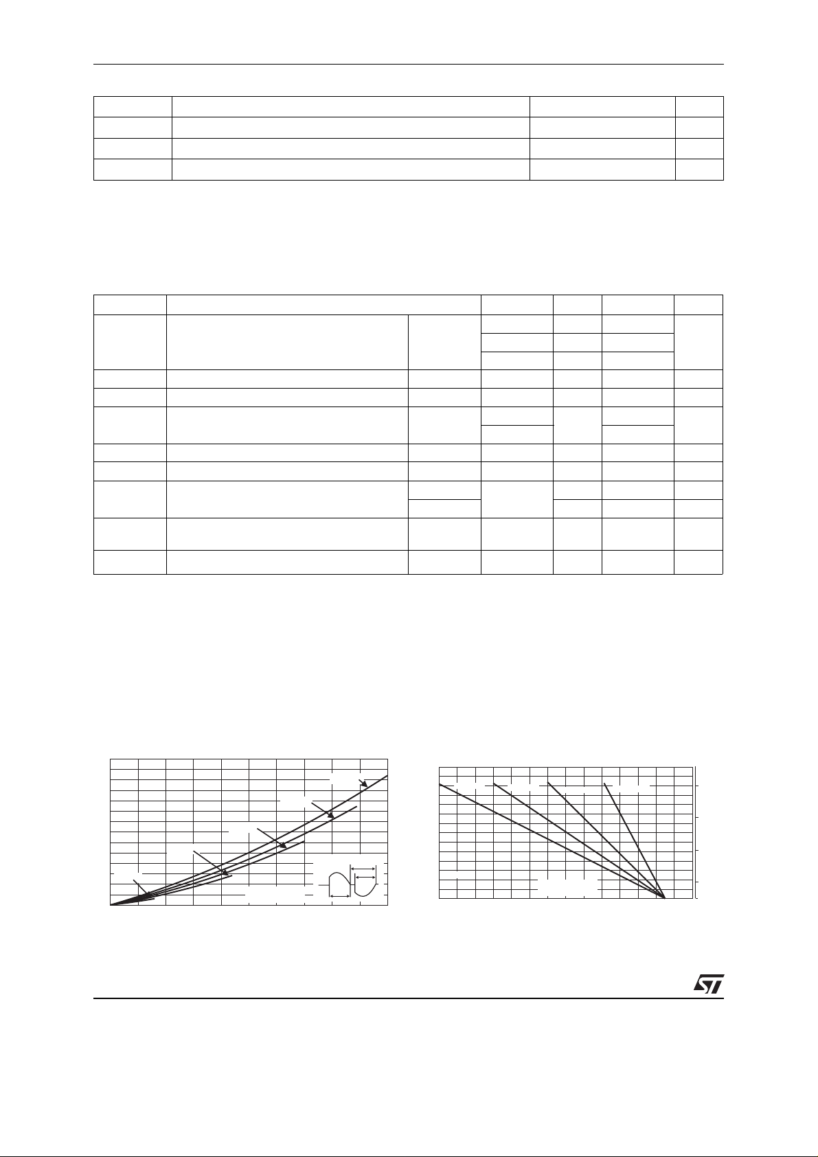
Fig. 1: Maximum power dissipation versus RMS
on-state current.
P(W)
35
30
25
20
15
α = 90°
α = 60°
α = 120°
10
α = 30°
5
0
0 5 10 15 20 25
IT(rms)(A)
α = 180°
α
180°
α
2/4
Fig. 2: Correlation between maximum power dissipation
and maximum allowable temperatures (T
T
) for different thermal resistances heatsink +
case
amb
and
contact.
Rth=0°C/W
Tcase (°C)
90
100
110
120
125
P(W)
35
Rth=3°C/W
30
25
20
15
10
α = 180°
5
0
0 20 40 60 80 100 120 140
Rth=2°C/W
Rth=1°C/W
Tamb(°C)
 Loading...