

Ordering number : ENN6472
32700RM (OT) No. 6472-1/14
Overview
The LC72348G/W and LC72349G/W are low-voltage
electronic tuning microcontrollers that include a PLL that
operates up to 230 MHz and a 1/4 duty 1/2 bias LCD
driver on chip. These ICs can contribute to further end
product cost reduction than the LC72341 series while
providing improved standby current characteristics. Also
these ICs can use the application program for the
LC72341 series except the IF counter function.
These ICs are optimal for use in low-voltage portable
audio equipment that includes a radio receiver.
Function
• Program memory (ROM):
— 3072 × 16 bits (6K bytes) LC72348G/W
— 4096 × 16 bits (8K bytes) LC72349 G/W
• Data memory (RAM):
— 192 × 4 bits LC72348 G/W
— 256 × 4 bits LC72349 G/W
• Cycle time: 40 µs (all 1-word instructions) at 75kHz
crystal oscillation
• Stack: 8 levels
• LCD driver: 48 to 80 segments (1/4 duty, 1/2 bias drive)
• Interrupts: One external interrupt
Timer interrupts (1, 5, 10, and 50 ms)
• A/D converter: Three input channels
(5-bit successive approximation
conversion)
• Input ports: 7 ports (of which three can be switched for
use as A/D converter inputs)
• Output ports: 6 ports (of which 1 can be switched for use
as the beep tone output and 2 are opendrain ports)
• I/O ports: 16 ports (of which 8 can be switched for use
as LCD ports and as mask options)
Continued on next page.
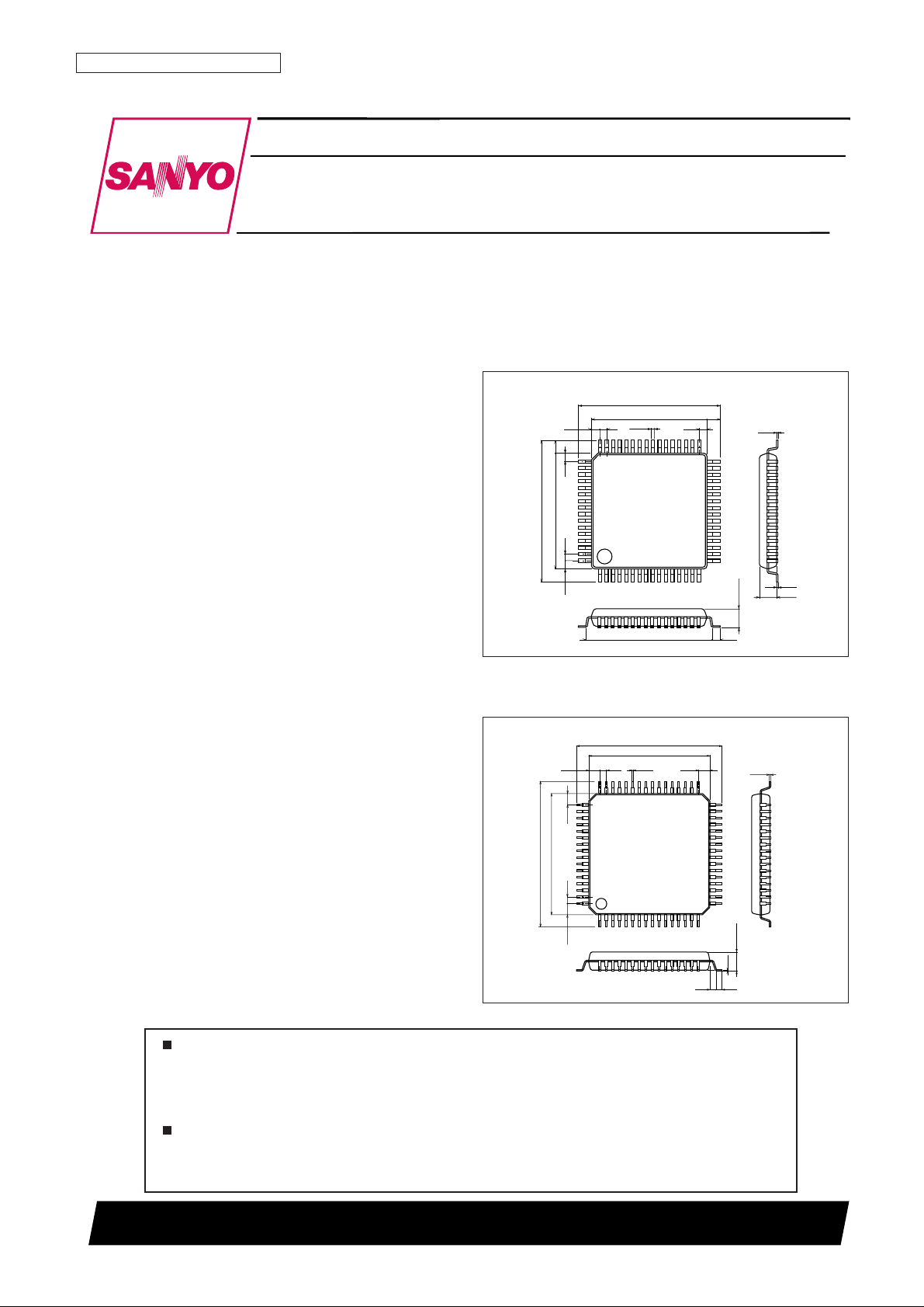
Package Dimensions
unit: mm
3231-QIP64G
10.0
12.0
1.25
0.5
1.25
1.25 0.5 1.250.18
12.0
116
17
32
33
48
49
64
10.0
0.5
1.7max
0.5
0.1
0.15
SANYO: SQFP64
[LC72348W, 72349W]
LC72348G/W, 72349G/W
SANYO Electric Co.,Ltd. Semiconductor Company
TOKYO OFFICE Tokyo Bldg., 1-10, 1 Chome, Ueno, Taito-ku, TOKYO, 110-8534 JAPAN
Low-Voltage ETR Controller
with On-Chip LCD Driver
CMOS IC
Any and all SANYO products described or contained herein do not have specifications that can handle
applications that require extremely high levels of reliability, such as life-support systems, aircraft’s
control systems, or other applications whose failure can be reasonably expected to result in serious
physical and/or material damage. Consult with your SANYO representative nearest you before using
any SANYO products described or contained herein in such applications.
SANYO assumes no responsibility for equipment failures that result from using products at values that
exceed, even momentarily, rated values (such as maximum ratings, operating condition ranges, or other
parameters) listed in products specifications of any and all SANYO products described or contained
herein.
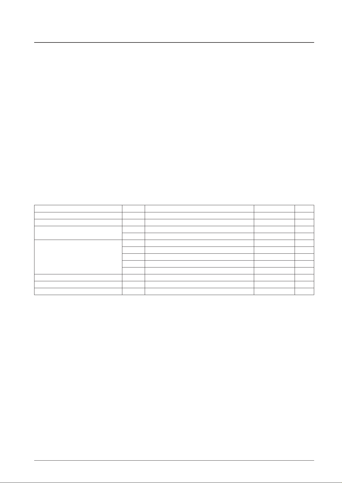
14.0
17.2
1.0
1.0
1.6
0.15
0.35
0.1
15.6
0.8
0.8
3.0max
116
17
32
33
48
49
64
2.15
14.0
17.2
1.0
1.0
1.6
0.8
SANYO: QFP64G
[LC72348G, 72349G]
unit: mm
3190-SQFP64
No. 6472-2/14
LC72348G/W, 72349G/W
Parameter Symbol Conditions Ratings Unit
Maximum supply voltage V
DD
max –0.3 to +4.0 V
Input voltage V
IN
All input pins –0.3 to VDD+0.3 V
Output voltage
V
OUT
(1) AOUT, PE –0.3 to +15 V
V
OUT
(2) All output pins except V
OUT
(1) –0.3 to VDD+ 0.3 V
I
OUT
(1) PC, PD, PG, PH, EO 0 to 3 mA
I
OUT
(2) PB 0 to 1 mA
Output current I
OUT
(3) AOUT, PE 0 to 2 mA
I
OUT
(4) S1 to S20 300 µA
I
OUT
(5) COM1 to COM4 3 mA
Allowable power dissipation Pdmax Ta = –20 to +70°C 300 mW
Operating temperature Topr –20 to +70 °C
Storage temperature Tstg –45 to +125 °C
Specifications
Absolute Maximum Ratings at Ta = 25°C, VSS= 0 V
Continued from preceding page.
• PLL: Supports dead zone control (two types)
• Reference frequencies: 1, 3, 3.125, 5, 6.25, 12.5,
and 25 kHz
• Input frequencies: FM band: 10 to 230 MHz
AM band: 0.5 to 10 MHz
• Input sensitivity:
FM band: 35 mVrms (50 mVrms at 130 MHz or higher
frequency)
AM band: 35 mVrms
• External reset input: During CPU and PLL operations,
instruction execution is started from
location 0.
• Built-in power-on reset circuit:
The CPU starts execution from location 0 when power is
first applied.
• Halt mode: The controller-operating clock is stopped.
• Backup mode: The crystal oscillator is stopped.
• Static power-on function: Backup state is cleared with
the PF port
• Beep tone: 1.5 and 3.1 kHz
• Built-in tuner voltage generating circuit:
Cost reduced in tuner-use power supply circuit
• Built-in low-pass filter amplifier
• Optional function switches:
— PH0 to PH3 (general-purpose input, open-drain
output/general-purpose input and output/S13 to S16)
— PG0 to PG3 (general-purpose input, open-drain
output/general-purpose input and output/S17 to S20)
— VSENSE circuit (provided/not provided)
— FM DC/DC clock (1/256, 75 kHz)
• Memory retention voltage: 0.9 V at least
• Package: SQFP-64 (0.5-mm pitch), QIC-64
(0.8-mm pitch)
No. 6472-3/14
LC72348G/W, 72349G/W
Parameter Symbol Conditions
Ratings
Unit
min typ max
V
DD
(1) PLL operating voltage 1.8 3.0 3.6
Supply voltage
V
DD
(2) Memory retention voltage 1.0
V
V
DD
(3) CPU operating voltage 1.4 3.0 3.6
V
DD
(4) A/D converter operating voltage 1.6 3.0 3.6
V
IH
(1)
Input ports other than V
IH
(2), VIH(3), AMIN,
0.7 V
DD
V
DD
V
Input high-level voltage
FMIN, and XIN
V
IH
(2) RES 0.8 V
DD
V
DD
V
V
IH
(3) Port PF 0.6 V
DD
V
DD
V
V
IL
(1)
Input ports other than V
IL
(2), VIL(3), AMIN,
0 0.3 V
DD
V
Input low-level voltage
FMIN, and XIN
V
IL
(2) RES 0 0.2 V
DD
V
V
IL
(3) Port PF 0 0.2 V
DD
V
V
IN
(1) XIN 0.5 0.6 Vrms
Input amplitude V
IN
(2) FMIN, AMIN 0.035 0.35 Vrms
V
IN
(3) FMIN 0.05 0.35 Vrms
Input voltage range V
IN
(5) ADIO, ADI1, ADI3 0 V
DD
V
F
IN
(1) XIN: CI ≤ 35 kΩ 70 75 80 kHz
Input frequency
F
IN
(2) FMIN: VIN(2), VDD(1) 10 130 MHz
F
IN
(3) FMIN: VIN(3), VDD(1) 130 250 MHz
F
IN
(4) AMIN(L): VIN(2), VDD(1) 0.5 10 MHz
Allowable Operating Ranges at Ta = –20 to +70°C, VDD= 1.8 to 3.6 V
Parameter Symbol Conditions
Ratings
Unit
min typ max
I
IH
(1) XIN: VI= VDD= 3.0 V 3 µA
Input high-level current
I
IH
(2) FMIN, AMIN: VI= VDD= 3.0 V 3 8 20 µA
PA/PF (without pull-down resistors), the PC,
IIH(3) PD, PG, and PH ports, and RES: VI= V
DD
3µA
= 3.0 V
IIL(1) XIN: VI= VDD= V
SS
–3 µA
Input low-level current
I
IL
(2) FMIN, AMIN: VI= VDD= V
SS
–3 –8 –20 µA
PA/PF (without pull-down resistors), the PC,
IIL(3) PD, PG, and PH ports, and RES: VI= V
DD
–3 µA
= V
SS
Input floating voltage V
IF
PA/PF (with pull-down resistors) 0.05 V
DD
V
Pull-down resistor values
R
PD
(1) PA/PF (with pull-down resistors), VDD= 3.0 V 75 100 200 kΩ
R
PD
(2) TEST1, TEST2 10 kΩ
Hysteresis V
H
RES 0.1 V
DD
0.2 V
DD
V
Voltage doubler reference voltage
DBR4
Referenced to V
DD
, C(3) = 0.47 µF,
1.3 1.5 1.7 V
Ta = 25°C *
1
Voltage doubler step-up voltage DBR1, 2, 3
C(1) = 0.47 µF
2.7 3.0 3.3 V
C(2) = 0.47 µF, without loading, Ta = 25°C *
1
VOH(1) PB: IO= –1 mA
V
DD
– VDD– V
0.7 V
DD
0.3 V
DD
VOH(2) PC, PD, PG, PH: IO= –1 mA
V
DD
–
V
0.3 V
DD
VOH(3) EO: IO= –500 µA
V
DD
–
V
Output high-level voltage 0.3 V
DD
VOH(4) XOUT: IO= –1 µA
V
DD
–
V
0.3 V
DD
VOH(5) S1 to S20: IO= –20 µA *
1
2.0 V
V
OH
(6)
COM1, COM2, COM3, COM4:
2.0 V
I
O
= –100 µA *
1
Electrical Characteristics within the allowable operating ranges
Continued on next page.
No. 6472-4/14
LC72348G/W, 72349G/W
Parameter Symbol Conditions
Ratings
Unit
min typ max
V
OL
(1) PB: IO= –50 µA 0.3 V
DD
0.7 V
DD
V
V
OL
(2) PC, PD, PE, PG, PH: IO= –1 mA 0.3 V
DD
V
V
OL
(3) EO: IO= –500 µA 0.3 V
DD
V
V
OL
(4) XOUT: IO= –1 µA 0.3 V
DD
V
Output low-level voltage V
OL
(5) S1 to S20: IO= –20 µA *
1
1.0 V
V
OL
(6)
COM1, COM2, COM3, COM4:
1.0 V
I
O
= –100 µA *
1
VOL(7) PE: IO= 2 mA 1.0 V
V
OL
(8) AOUT(AIN = 1.3 V), TU: IO= 1 mA, VDD= 3 V 0.5 V
Output off leakage current
I
OFF
(1) Ports PB, PC, PD, PG, PH, and EO –3 +3 µA
I
OFF
(2) AOUT and port PE –100 +100 nA
A/D converter error ADI0, ADI1, ADI3 V
DD
(4) –1/2 +1/2 LSB
Supply voltage drop detection voltage V
SENSE
(1) Ta = 25°C *
2
1.6 1.75 1.9 V
Supply voltage rise detection voltage V
SENSE
(2) Ta = 25°C *
2
(1)min (1)max
V
+0.1 +0.2
IDD(1) VDD(1): FIN(2) 130 MHz, Ta = 25°C 5 15 mA
I
DD
(2) VDD(2): In HALT mode, Ta = 25°C *
3
0.1 mA
Current drain I
DD
(3)
V
DD
= 3.6 V, with the oscillator stopped,
1µA
Ta = 25°C *
4
IDD(4)
V
DD
= 1.8 V, with the oscillator stopped,
0.5 µA
Ta = 25°C *
4
Note: The halt mode current is due to the CPU executing 20 instruction steps every 125 ms.
Continued from preceding page.
Pin Assignment
616263
DBR3
DBR2
DBR1
RES
TU
VDD
DBR4
PD1
INT/PD0
PE1
BEEP/PE0
ADI3/PF2
ADI1/PF1
ADI0/PF0
VSS
PG3/S20
PG2/S19
PG1/S18
PG0/S17
PH3/S16
PH2/S15
PH1/S14
PH0/S13
AMIN
VSS
EO
AOUT
AIN
AGND
TEST1
XIN
FMIN
64 585960 555657 525354 495051
48
47
46
45
44
43
42
41
40
39
38
37
36
35
3415
16 33
31
32
29
30
27
28
25
26
23
24
21
22
19
20
17
18
13
14
11
12
9
10
7
8
5
6
3
4
COM1XOUT
1
COM2TEST2
COM3PA3
COM4PA2
S1PA1
S2PA0
S3
PB3
S4PB2
LC72348G, 72348W
LC72349G, 72349W
S5PB1
S6
PB0
S7PC3
S8PC2
S9PC1
S10PC0
S11PD3
PD2 S12
2
Note: * C(1), C(2), and C(3) must be connected even if an LCD is not used.
No. 6472-5/14
LC72348G/W, 72349G/W
DBR1
DBR2
DBR3
0.1 to 1 µF
0.1 to 1 µF
0.1 to 1 µF
C(C1)
C(C2)
DBR4
C(C3)
Notes: *1. The capacitors C(1), C(2), and C(3) must be connected to the DBR pins.
*2. V
SENSE
When the VDDvoltage drops, the V
SENSE
flag is set when that voltage is 1.75 V (typical). Applications can
check the V
SENSE
flag using the TST instruction. Battery or other power source depletion can be easily
measured by monitoring this flag.
Note that the voltage for V
SENSE
detection differs for the falling and rising directions. Thus, after the V
SENSE
flag has been set due to a voltage drop, it will not be reset if the voltage rises by under 0.1 V.
V
DD
t
1.9 V
1.6 V
→ SETRESET←
V
DD
t
2.1 V
1.7 V
→RESETSET←
AA
7 pF 7 pF
FMIN
XIN
AMIN
TEST1, 2
XOUT
VDD
DBR2
DBR1
DBR1
0.1 µF
0.1 µF
0.1 µF
0.1 µF
0.1 µF
0.1 µF
DBR3
DBR4
RESRES
VSS
PA, PF
AGND
AIN
FMIN
XIN
AMIN
TEST1, 2
XOUT VDD
VSS
AGND
AIN
7pF
75 kHz 75 kHz
7pF
DBR2
DBR3
DBR4
V
SENSE
(1)
For a falling voltage
*3. Halt mode current measurement circuit *4. Backup mode current measurement circuit
With all ports other than those specified above left open.
With output mode selected for PC and PD.
With segments S13 to S20 selected.
With all ports other than those specified above left open.
With output mode selected for PC and PD.
With segments S13 to S20 selected.
V
SENSE
(2)
For a rising voltage
 Loading...