

Ordering number : ENN6171
31000RM (OT) No. 6171-1/13
Overview
The LC72344W and LC72345W are low-voltage
electronic tuning microcontrollers that include a DC-DC
converter, a PLL that operates up to 230 MHz, a 1/4 duty
1/2 bias LCD driver and other functions on chip. The
built-in DC-DC converter provided by these ICs can easily
implement a tuning system voltage generator circuit, and
furthermore, since the transistor required for the low-pass
filter is built in, these ICs can contribute to further end
product cost reductions. Additionally, the DC-DC
converter output voltage can be provided to other external
ICs, making these products optimal for low-voltage
portable audio equipment that includes a radio receiver.
Functions
• Program memory (ROM): 3072 × 16 bits (6 KB)
LC72344W
4096 × 16 bits (8 KB)
LC72345W
• Data memory (RAM): 192 × 4 bits LC72344W
256 × 4 bits LC72345W
• Cycle time: 40 µs (all 1-word instructions)
• Stack: 8 levels
• LCD driver: 48 to 76 segments (1/4 duty, 1/2 bias drive)
• Interrupts: One external interrupt
Timer interrupts (1, 5, 10, and 50 ms)
• A/D converter: Two input channels (5-bit successive
approximation conversion)
• Input ports: 6 ports (of which 2 can be switched for use
as A/D converter inputs)
• Output ports: 6 ports (of which 1 can be switched for use
as the beep tone output and 2 are opendrain ports)
• I/O ports: 16 ports (of which 8 can be switched for use
as LCD ports as mask options)
(Continued on next page.)
LC72344W, 72345W
SANYO Electric Co.,Ltd. Semiconductor Company
TOKYO OFFICE Tokyo Bldg., 1-10, 1 Chome, Ueno, Taito-ku, TOKYO, 110-8534 JAPAN
Low-Voltage ETR Controller with On-Chip DC-DC
Converter
CMOS IC
Any and all SANYO products described or contained herein do not have specifications that can handle
applications that require extremely high levels of reliability, such as life-support systems, aircraft’s
control systems, or other applications whose failure can be reasonably expected to result in serious
physical and/or material damage. Consult with your SANYO representative nearest you before using
any SANYO products described or contained herein in such applications.
SANYO assumes no responsibility for equipment failures that result from using products at values that
exceed, even momentarily, rated values (such as maximum ratings, operating condition ranges, or other
parameters) listed in products specifications of any and all SANYO products described or contained
herein.
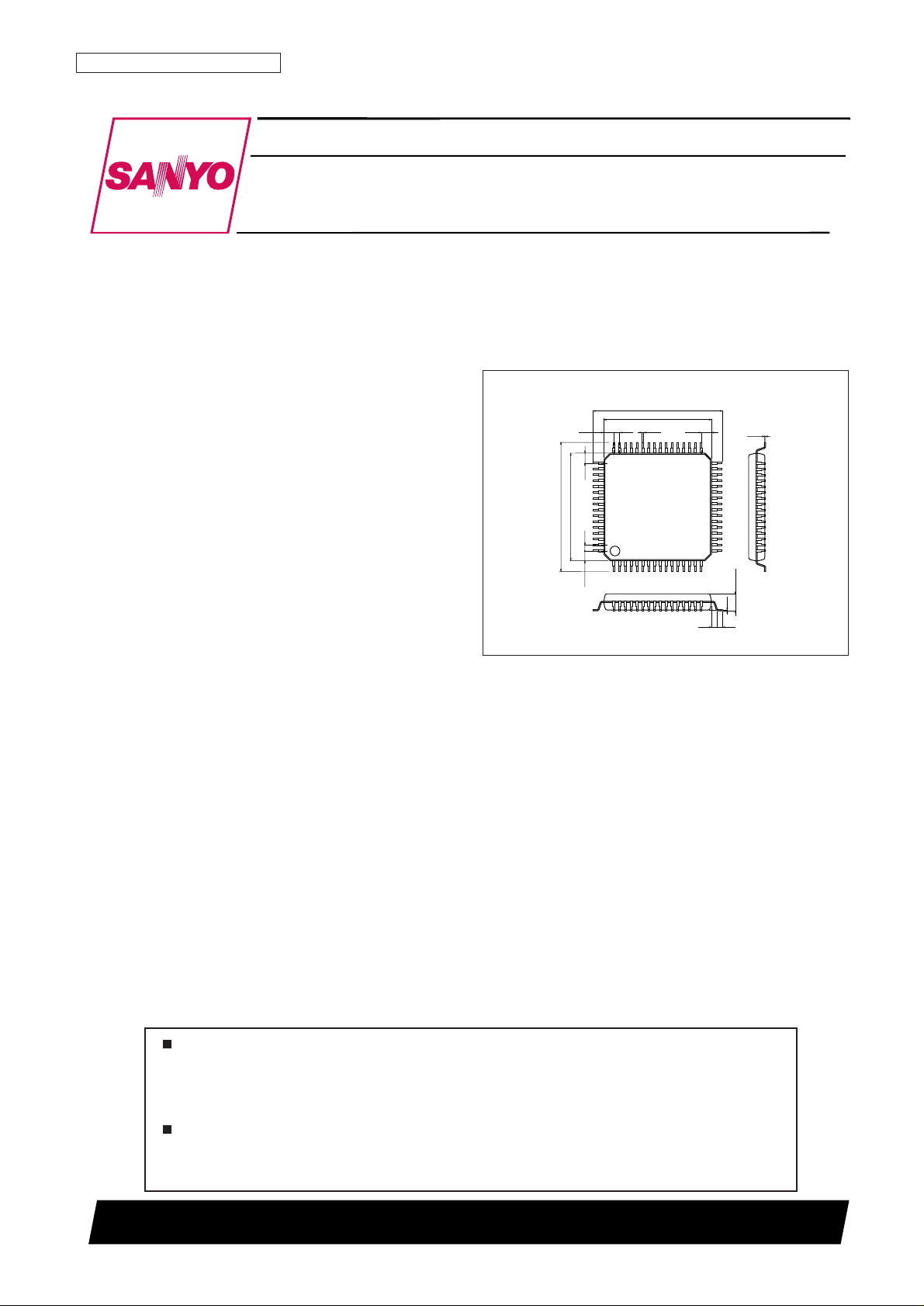
Package Dimensions
unit: mm
3190-SQFP64
10.0
12.0
1.25
0.51.25
1.25 0.5 1.250.18
12.0
116
17
32
33
48
49
64
10.0
0.5
1.7max
0.5
0.1
0.15
SANYO: SQFP64
[LC72344W, 72345W]

(Continued from preceding page.)
• PLL: Supports dead band control (two types)
Reference frequencies: 1, 3, 5, 6.25, 12.5, and 25 kHz
• Input frequencies: FM band: 10 to 230 MHz
AM band: 0.5 to 10 MHz
• Input sensitivity: FM band: 35 mV rms (50 mV rms at
130 MHz or higher frequency)
AM band: 35 mV rms
• External reset input: During CPU and PLL operation,
instruction execution is started
from location 0.
• Built-in power-on reset circuit:
The CPU starts executing from location 0 when power
is first applied.
• Static power-on function: Backup state clear function
using the BATT pin.
• Halt mode: The controller operating clock is stopped.
• Backup mode: The crystal oscillator is stopped.
• Beep tone: 1.5 and 3.1 kHz
• Built-in DC-DC converter:
Two systems (One system
can be used as an external circuit power supply by
providing an external transistor.)
• Built-in low-pass filter amplifier: An external low-pass
filter amplifier circuit is no longer required in end
products.
• Remaining power check function: The battery voltage
can be directly converted to a digital value by the A/D
converter.
• Memory retention voltage: 0.9 V or higher.
•VDDvoltage: 0.9 to 1.8 V
• Package: SQFP-64 (0.5 mm lead pitch)
No. 6171-2/13
LC72344W, 72345W
LC72344W
LC72345W
XIN
TEST1
AGND
AOUT
AIN
EO
VSS
AMIN
FMIN
VDD
BRES
COM1
COM3
COM2S1COM4
XOUT
TEST2
PA3
PA2
PA1
PA0
PB3
PB2
PB1
PB0
PC3
PD3
PC2
PC1
PC0
PD2
PD1
PG2/S18
S2
S5
S7
S9
S12/PH0
S11
S8
S6
S4
S3
S10
S13/PH1
S15/PH3
S14/PH2
S17/PG1
(Top view)
S16/PG0
1
2
3
4
5
6
7
8
11
9
10
14
15
12
16
13
17
PE1
INT/PD0
BEEP/PE0
BATT
ADI0/PF0
ADI1/PF1
VDC1
VDC3
VSS
VDC2
VREF
VCON
VADJ
PG3/S19
32
19
18
20
21
22
23
24
25
28
30
31
29
27
26
48
47
45
46
43
44
41
39
40
42
36
37
38
35
33
34
52
50
53
61
54
55
57
49
56
59
58
51
60
63
62
64
Pin Assignment
No. 6171-3/13
LC72344W, 72345W
Parameter Symbol Conditions Ratings Unit
V
DD
(1)max VDD –0.3 to +0.3 V
Maximum supply voltage
V
DD
(2)max VDC1 –0.3 to +4.0 V
V
DD
(3)max VDC2 –0.3 to +4.0 V
V
DD
(4)max VDC3 –0.3 to +4.0 V
Input voltage
V
IN
(1) PF, FMIN, AMIN, AIN, BATT, and BRES –0.3 to VDD(3) to +0.3 V
V
IN
(2) PA, PC, PD, PG, and PH –0.3 to VDD(1) to +0.3 V
V
OUT
(1) AOUT, and PE –0.3 to +15 V
Output voltage
V
OUT
(2) PB, PC, PD, PG, and PH –0.3 to VDD(1) +0.3 V
V
OUT
(3) VREF, and EO –0.3 to VDD(3) +0.3 V
V
OUT
(4) COM1 to COM4, S1 to S19 –0.3 to VDD(4) +0.3 V
I
OUT
(1) PC, PD, PG, PH, and EO 0 to 3 mA
I
OUT
(2) PB 0 to 1 mA
Output current I
OUT
(3) AOUT, and PE 0 to 2 mA
I
OUT
(4) S1 to S20 300 µA
I
OUT
(5) COM1 to COM4 3 mA
Allowable power dissipation Pdmax Ta = –20 to +70°C 200 mW
Operating temperature Topr –20 to +70 °C
Storage temperature Tstg –45 to +125 °C
Specifications
Absolute Maximum Ratings at Ta = 25°C, VSS= 0 V
Parameter Symbol Conditions
Ratings
Unit
min typ max
V
DD
(1) The voltage applied to the VDD pin 0.9 1.5 1.8 V
V
DD
(2) The voltage applied to the VDC1 pin 0.9 1.5 1.8 V
Supply voltage V
DD
(3) The voltage applied to the VDC2 pin 1.8 2.1 2.4 V
V
DD
(4) The voltage applied to the VDC3 pin 2.6 3.0 3.4 V
V
DD
(5) Memory retention voltage 0.9 V
V
IH
(1) Ports PC, PD, PG, and PH 0.7 VDD(1) VDD(1) V
Input high-level voltage
V
IH
(2) Port PA 0.8 VDD(1) VDD(1) V
V
IH
(3) Port PF 0.8 VDD(1) VDD(3) V
V
IH
(4) Ports BRES and BATT 0.6 VDD(1) VDD(3) V
V
IL
(1) Ports PC, PD, PG, and PH 0 0.3 VDD(1) V
Input low-level voltage
V
IL
(2) Port PA 0 0.2 VDD(1) V
V
IL
(3) Port PF 0 0.2 VDD(1) V
V
IL
(4) Ports BRES and BATT 0 0.2 VDD(1) V
V
IN
(1) XIN 0.5 0.6 Vrms
Input amplitude V
IN
(2) FMIN, AMIN: VDD(3) = 2.1 V 0.035 0.35 Vrms
V
IN
(3) FMIN: VDD(3) = 2.1 V 0.05 0.35 Vrms
Input voltage range V
IN
(4) ADI0, ADI1, and V
DD
0V
DD
(4) V
F
IN
(1) XIN: CI ≤ 35 kΩ 70 75 80 kHz
Input frequency
F
IN
(2) FMIN: VIN(2), VDD(3) = 2.1 V 10 130 MHz
F
IN
(3) FMIN: VIN(3), VDD(3) = 2.1 V 130 230 MHz
F
IN
(4) AMIN(L): VIN(2), VDD(3) = 2.1 V 0.5 10 MHz
Allowable Operating Ranges at Ta = –20 to +70°C, VDD= 0.9 to 1.8 V
No. 6171-4/13
LC72344W, 72345W
Parameter Symbol Conditions
Ratings
Unit
min typ max
I
IH
(1) XIN: VDD(1) = 1.8 V, VDD(2) = 1.8 V, VDD(3) = 2.1 V 3 µA
I
IH
(2) FMIN, and AMIN: VDD(3) = 2.1 V 3 8 20 µA
Input high-level voltage I
IH
(3) Ports BRES, BATT, and PF: VDD(3) = 2.1 V 4 µA
I
IH
(4)
Ports PA (no pull-down resistor), PC, PD, PG, and PH:
3µA
V
DD
(1) = 1.8 V
I
IL
(1) XIN: VDD(1) = VDD(2) = VDD(3) = V
SS
–3 µA
I
IL
(2) FMIN, and AMIN: VDD(3) = V
SS
–3 –8 –20 µA
Input low-level voltage I
IL
(3) Ports BRES, BATT, and PF: VDD(3) = V
SS
–4 µA
I
IL
(4)
Ports PA (no pull-down resistor), PC, PD, PG, and PH:
–3 µA
V
DD
(1) = V
SS
Input floating voltage V
IF
Port PA pull-down resistor present
0.05 VDD(1)
V
Pull-down resistor
R
PD
(1) Port PA pull-down resistor: VDD(1) = 1.3 V 75 100 200 kΩ
R
PD
(2) TEST1 and TEST2 pull-down resistors 10 kΩ
Hysteresis V
H
BRES 0.1 VDD(3) 0.2 VDD(3) V
V
OH
(1) PB: IO= 1 mA
V
DD
(1) – VDD(1) –
V
0.7 V
DD
(1) 0.3 VDD(1)
V
OH
(2) PC, PD, PG, PH: IO= 1 mA
V
DD
(1) –
V
0.3 V
DD
(1)
V
OH
(3) EO: IO= –500 µA
V
DD
(3) –
V
Output high-level voltage 0.3 V
DD
(3)
V
OH
(4) XOUT IO= 1 µA
V
DD
(3) –
V
0.3 V
DD
(3)
V
OH
(5) S1 to S20: IO= 20 µA VDD(4) – 1 V
V
OH
(6) COM1, CM2, COM3, and COM4: IO= 100 µA VDD(4) – 1 V
V
OH
(7) VREF: IO= 1 mA VDD(3) – 1 V
V
OL
(1) PB: IO= –50 µA 0.3 VDD(1) 0.7 VDD(1) V
V
OL
(2) PC, PD, PG, and PH: IO= –1 mA 0.3 VDD(1) V
V
OL
(3) EO: IO= –500 µA 0.3 VDD(3) V
Output low-level voltage
V
OL
(4) XOUT: IO= –1 µA 0.3 VDD(3) V
V
OL
(5) S1 to S20: IO= –20 µA VDD(4)–2 V
V
OL
(6) COM1, COM2, COM3, and COM4: IO= –100 µA VDD(4)–2 V
V
OL
(7) PE: IO= 2 mA 0.6 VDD(1) V
V
OL
(8) AOUT: IO= 1 mA, AIN = 1.3 V: VDD(4) = 3 V 0.5 V
Output off leakage current
I
OFF
(1) PB, PC, PD, PG, PH, and E0 ports –3 3 µA
I
OFF
(2) AOUT and PE ports –100 100 nA
A/D converter error ADI0 and ADI1, V
DD
–1/2 +1/2 LSB
Internal clock frequency
fosc(1) FM, and PLLSTOP: V
DD
(3) = 2.1 V, Vcon = OPEN 300 600 900 kHz
fosc(2) AM 450 1200 kHz
I
DD1
(1)
V
DD
(1) = 1.5 V, VDD(3) = 2.1 V, VDD(4) = 3.0 V:
1mA
F
IN
(2) 130 MHz, Ta = 25°C
I
DD2
(2)
V
DD
(1) = 1.5 V, VDD(3) = 2.1 V, VDD(4) = 3.0 V:
5mA
F
IN
(2) 130 MHz, Ta = 25°C
I
DD3
(3)
V
DD
(1) = 1.5 V, VDD(3) = 2.1 V, VDD(4) = 3.0 V:
1mA
F
IN
(2) 130 MHz, Ta = 25°C
I
DD1
(4)
V
DD
(1) = 1.5 V, VDD(3) = 2.1 V, VDD(4) = 3.0 V:
0.1 mA
Halt mode, Ta = 25°C *1
Current drain
I
DD2
(5)
V
DD
(1) = 1.5 V, VDD(3) = 2.1 V, VDD(4) = 3.0 V:
0.3 mA
Halt mode, Ta = 25°C *1
I
DD3
(6)
V
DD
(1) = 1.5 V, VDD(3) = 2.1 V, VDD(4) = 3.0 V:
0.1 mA
Halt mode, Ta = 25°C *1
I
DD1
(7)
V
DD
(1) = 1.5 V, VDD(3) = 2.1 V, VDD(4) = 3.0 V:
100 nA
With the oscillator stopped, Ta = 25°C *
I
DD2
(8)
V
DD
(1) = 1.5 V, VDD(3) = 2.1 V, VDD(4) = 3.0 V:
500 nA
With the oscillator stopped, Ta = 25°C *
I
DD3
(9)
V
DD
(1) = 1.5 V, VDD(3) = 2.1 V, VDD(4) = 3.0 V:
100 nA
With the oscillator stopped, Ta = 25°C *
Electrical Characteristics under allowable operating conditions
The halt mode current drain is due to 20 instructions being executed every 125 ms.

No. 6171-5/13
LC72344W, 72345W
*1 Halt mode current drain test conditions *2 Backup mode current drain test conditions
Leave all ports other than those mentioned above open.
Select output mode for PC and PD.
Select the segment function for S12 to S19.
A A
7 pF
FMIN
XIN
AMIN
TEST1, 2
XOUT
VDD
VDC2
VDC3
RES
VSS
PA,PF
AGND
AIN
Leave all ports other than those mentioned above open.
Select output mode for PC and PD.
Select the segment function for S12 to S19.
7 pF
75 kHz
BATT
2.2 V
3 V
A
A
1.5 V
IDD1
IDD3
IDD2
2.2 V
3 V
A
A
IDD3
IDD2
7 pF
FMIN
XIN
AMIN
TEST1, 2
XOUT
VDD
VDC2
VDC3
RES
VSS
AGND
AIN
7 pF
75 kHz
BATT
1.5 V
IDD1

No. 6171-6/13
LC72344W, 72345W
PHASE
DETECTOR
REFERENCE DIVIDERDIVIDER
SYSTEM CLOCK
GENERATOR
PROGRAMMBLE DIVIDER
1/16,1/17
SEG
LA
P-ON
RESET
1/2
TIME BASE
CONTROL
UNIVERSAL
COUNTER
(20 bits)
BANK
COUNT
END
ADDRESS
DECODER
DATA BUS
TIMER 0
JUDGE
ALU
CF
SKIP
BANK
LATCH
A
STACK
4
14
14
ADDRESS COUNTER
ADDRESS DECORDER
ROM
3k × 16 bits
(LC72344)
4k × 16 bits
(LC72345)
BUS
CONTROL
JMP
CAL
RETURN
INTERRUPT
RESET
INSTRUCTION
DECODER
PLL DATA LATCH
PLL CONTROL
DATA
LATCH
/
BUS
DRIVER
DATA
LATCH
/
BUS
DRIVER
BUS
DRIVER
XIN
XOUT
FMIN
PC2
PC1
PC0
PC3
PA3
PA2
PA1
PA0
TEST2
TEST1
RES
*
AMIN
S15/PH0
S14/PH1
S12/PH3
S13/PH2
LCD
PORT
DRIVER
LCPA/B
LCDA/B
EO
S11
S1
VSS
PB2
PB1
PB0
PB3
*
DATA
LATCH
/
BUS
DRIVER
PD2
PD1
INT/PD0
AGND
AOUT
AIN
PD3
LATCH
B
PE0/BEEP
COM1
COM2
COM3
COM4
S19/PG0
S18/PG1
S16/PG3
S17/PG2
DATA
LATCH
/
BUS
DRIVER
MPX
(5 bits)
MPX
MPX
BEEP TONE
COMMON
DRIVER
DATA
LATCH
/
BUS
DRIVER
DATA
LATCH
/
BUS
DRIVER
DATA
LATCH
/
BUS
DRIVER
7 80
BATT
PF1/ADI1
PF0/ADI0
PE0/BEEP
VDC3
VDC1
VDC2
VCON
VREF
VADJ
VDD
RC OSCILLATOR
CIRCUIT
1/2
1/2
1/2
RAM
192 × 4 bits
(LC72344)
256 × 4 bits
(LC72345)
Block Diagram
No. 6171-7/13
LC72344W, 72345W
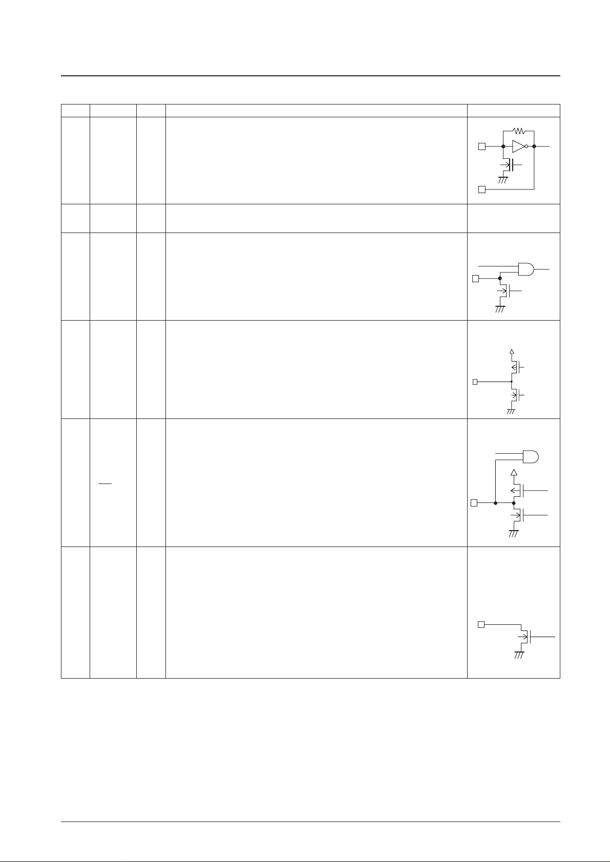
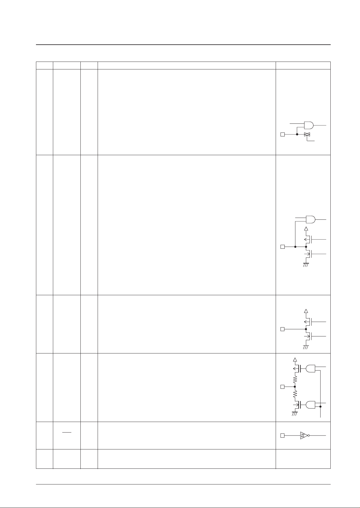
Pin Functions
Pin No. Pin I/O Function I/O circuit
75 kHz crystal oscillator connections
64
1
XIN
XOUT
I
O
IC testing.
These pins must be connected to ground.
—
63
2
TEST1
TEST2
I
I
Input with built-in
pull-down resistor
Special-purpose ports for key return signal input designed with a low threshold voltage. When
a key matrix is formed in combination with port PB, simultaneous multiple key presses with
up to 3 keys can be detected. The pull-down resistors are set up for all four pins at the same
time with the IOS instruction (PWn = 2.b1). This setting cannot be specified for individual
pins. In backup mode, these pins go to the input disabled state, and the pull-down resistors
are disabled after a reset.
6
5
4
3
PA0
PA1
PA2
PA3
I
Unbalanced CMOS
push-pull output
Unbalanced CMOS outputs. These outputs are switched with the IOS 0 instruction. Since
these outputs are unbalanced, no diodes are required to prevent short circuits due to
simultaneous multiple key presses. These outputs go to the high-impedance output state in
backup mode. After a reset, they go to the high-impedance output state and remain in that
state until an output instruction (OUT, SPB, or RPB) is executed.
10
9
8
7
PB0
PB1
PB2
PB3
O
CMOS push-pull output
General-purpose I/O ports.
PD0 can be used as an external interrupt port. The IOS instruction (Pwn = 4, 5) is used for
switching the general-purpose I/O port function, and these ports can be set to input or output
in 1-bit units. (0: input, 1: output)
In backup mode they go to the input disabled high-impedance state.
After a reset, they switch to the general-purpose input port function.
14
13
12
11
18
17
16
15
PC0
PC1
PC2
PC3
INT/PD0
PD1
PD2
PD3
(*)
I/O
N-channel open-drain output
General-purpose output and beep tone output shared function ports (PE0 only). The BEEP
instruction is used to switch PE0 between the general-purpose output port and beep tone
output functions. To use PE0 as a general-purpose output port, execute a BEEP instruction
with b2 set to 0. Set b2 to 1 to use PE0 as the beep tone output port. The b0 and b1 bits are
used to select the beep tone frequency. There are two beep tone frequencies supported.
*: When PE0 is set up as the beep tone output, executing an output instruction to PN0 only
changes the state of the internal output latch, it does not affect the beep tone output in any
way. Only the PE0 pin can be switched between the general-purpose output function and the
beep tone output function; the PE1 pin only functions as a general-purpose output. These
pins go to the high-impedance state in backup mode and remain in that state until an output
instruction or a BEEP instruction is executed. Since these ports are open-drain ports,
resistors must be inserted between these pins and V
DD
. These ports are set to their general-
purpose output port function after a reset.
2019BEEP/PE0
PE1
Continued on next page.
No. 6171-8/13
LC72344W, 72345W
Continued from preceding page.
Pin No. Pin I/O Function I/O circuit
General-purpose input and A/D converter input shared function ports.
The IOS instruction (Pwn = FH) is used to switch between the general-purpose input and A/D
converter port functions. The general-purpose input and A/D converter port functions can be
switched in a bit units, with 0 specifying general-purpose input, and 1 specifying the A/D
converter input function. To select the A/D converter function, set up the A/D converter pin
with an IOS instruction with Pwn set to 1. The A/D converter is started with the UCC
instruction (b3 = 1, b2 = 1). The ADCE flag is set when the conversion completes. The INR
instruction is used to read in the data.
*: If an input instruction is executed for one of these pins which is set up for analog input, the
read in data will be at the low level since CMOS input is disabled. In backup mode these pins
go to the input disabled high-impedance state. These ports are set to their general-purpose
input port function after a reset. The A/D converter is a 5-bit successive approximation type
converter, and features a conversion time of 1.28 ms. Note that the full-scale A/D converter
voltage (1FH) is (63/96) times VDC3.
2322PF0/ADI0
PF1/ADI1
I
CMOS input/analog input
LCD driver segment output and general-purpose I/O shared function ports.
The IOS instruction* is used for switching both between the segment output and general-
purpose I/O functions and between input and output for the general-purpose I/O port function.
• When used as segment output ports
The general-purpose I/O port function is selected with the IOS instruction (Pwn = 8).
b0 = S16 to 19/PG0 to 3 (0: Segment output, 1: PG0 to 3)
The general-purpose I/O port function is selected with the IOS instruction (Pwn = 9).
b0 = S12 to 15/PH0 to 3 (0: Segment output, 1: PH0 to 3)
• When used as general-purpose I/O ports
The IOS instruction (Pwn = 6,7) is used to select input or output. Note that the mode can
be set in a bit units.
b0 = PG0 b0 = PH0
b1 = PG1 0: Input b1 = PH1 0: Input
b2 = PG2 1: Output b2 = PH2 1: Output
b3 = PG3 b3 = PH3
In backup mode, these pins go to the input disabled high-impedance state if set up as
general-purpose outputs, and are fixed at the low level if set up as segment outputs. These
ports are set up as segment outputs after a reset.
Although the general-purpose port/LCD port setting is a mask option, the IOS instruction
must be used as described above to set up the port function.
31
32
33
34
35
36
37
38
PG3/S19
PG2/S18
PG1/S17
PG0/S16
PH3/S15
PH2/S14
PH1/S13
PH0/S12
(*)
() ()
O
CMOS push-pull output
LCD driver segment output pins.
A 1/4-duty 1/2-bias drive technique is used.
The frame frequency is 75 Hz.
In backup mode, these outputs are fixed at the low level.
After a reset, these outputs are fixed at the low level.
39 to 49 S11 to S1 O
CMOS push-pull output
LCD driver common output pins.
A 1/4-duty 1/2-bias drive technique is used.
The frame frequency is 75 Hz.
In backup mode, these outputs are fixed at the low level.
After a reset, these outputs are fixed at the low level.
50
51
52
53
COM4
COM3
COM2
COM1
O
System reset input.
In CPU operating mode or halt mode, applications must apply a low level for at least one full
machine cycle to reset the system and restart execution with the PC set to location 0. This
pin is connected in parallel with the internal power on reset circuit.
54 RES I
Battery presence/absence discrimination.
The internal clock oscillator starts when a high level is input to this pin.
The IN instruction can be used to determine whether or not a battery is present.
21 BATT I
Continued on next page.

No. 6171-9/13
LC72344W, 72345W
Continued from preceding page.
Pin No. Pin I/O Function I/O circuit
VDC3 (3 V) step-up control.24 VDC1 I
CMOS amplifier input
2.1 V power supply. Apply either the voltage stepped-up by the DC-DC converter or an
equivalent voltage (2.1 V typical).
27 VDC2 I
3 V power supply. Apply either the voltage stepped-up by VDC1 or an equivalent voltage (3 V
typical).
25 VDC3 I
VDC2 step-up transistor drive.28 VREF O
Frequency adjustment for the internal RC oscillator circuit. The RC oscillator frequency can
be lowered by inserting a capacitor between this pin and ground.
29 VCON I
The VDC3 voltage can be adjusted by inserting a resistor between this pin and ground.30 VADJ O
FM VCO (local oscillator) input.
This pin is selected with the PLL instruction CW1.
The input must be capacitor coupled.
Input is disabled in backup mode, in halt mode, after a reset, and in PLL stop mode.
56 FMIN I
CMOS amplifier input
AM VCO (local oscillator) input.
This pin and the bandwidth are selected with the PLL instruction CW1.
The input must be capacitor coupled.
Input is disabled in backup mode, in halt mode, after a reset, and in PLL stop mode.
57 AMIN I
CMOS push-pull output
Main charge pump output. When the local oscillator frequency divided by N is higher than the
reference frequency a high level is output, when lower, a low level is output, and the pin is set
to the high-impedance state when the frequencies match.
This output goes to the high-impedance state in backup mode, in halt mode, after a reset,
and in PLL stop mode.
59 EO O
Transistor used for the low-pass filter amplifier.
Connect AGND to ground.
60
61
62
AIN
AOUT
AGND
O
Power supply pin.
This pin must be connected to ground.
This pin must be connected to ground.
This pin must be connected to VDD. Supports A/D converter.
—
26
58
55
VSS
VSS
VDD
—
CW1 b1, b0 Bandwidth
11 0.5 to 10 MHz (MW, LW)
Note: *Applications must establish the output data in advance with an OUT, SPB, or RPB instruction and then set the pin to output mode with an IOS
instruction when using the I/O switchable ports as output pins.

VDC3
VDC1
+
LCD, A/D converter,
and power reset
3 V system
comparator
VDC2
VREF
+
2.1 V system
comparator
Internal
power
supply
VADJ
Reference voltage
RC oscillator
VCON
VDD
Local AM signal
Supply voltage (0.9 to 1.8 V)
IC internal circuits
EO
AIN
AOUT
AGND
Varactor
TU+B
TU+B
FM mode AM mode
IC internal circuits
DC-DC Converter Application Sample
Low-Pass Filter Application Sample
No. 6171-10/13
LC72344W, 72345W

LC72344W and LC72345W Instruction Set
Terminology
ADDR : Program memory address
b : Borrow
C : Carry
DH : Data memory address High (Row address) [2 bits]
DL : Data memory address Low (Column address) [4 bits]
I : Immediate data [4 bits]
M : Data memory address
N : Bit position [4 bits]
Rn : Resister number [4 bits]
Pn : Port number [4 bits]
PW : Port control word number [4 bits]
r : General register (One of the address from 00H to 0FH of BANKO)
( ), [ ] : Contents of register or memory
M (DH, DL) : Data memory specified by DH, DL
No. 6171-11/13
LC72344W, 72345W
Mnemonic
Operand
Function Operational function
Instruction format
1st 2nd
AD r M Add M to r r ← (r) + (M)
ADS r M Add M to r, then skip if carry r ← (r) + (M), skip if carry
AC r M Add M to r with carry r ← (r) + (M) + C
ACS r M
Add M to r with carry, r ← (r) + (M) + C
then skip if carry skip if carry
AI M I Add I to M M ← (M) + I
AIS M I Add I to M, then skip if carry M ← (M) + I, skip if carry
AIC M I Add I to M with carry M ← (M) + I + C
AICS M I
Add I to M with carry, M ← (M) + I + C,
then skip if carry skip if carry
SU r M Subtract M from r r ←(r) – (M)
SUS r M
Subtract M from r, r ← (r) – (M),
then skip if borrow skip if borrow
SB r M Subtract M from r with borrow r ← (r) – (M) – b
SBS r M
Subtract M from r with borrow, r ← (r) – (M) – b,
then skip if borrow skip if borrow
SI M I Subtract I from M M ← (M) – I
SIS M I
Subract I from M, M ← (M) – I,
then skip if borrow skip if borrow
SIB M I Subtract I from M with borrow M ← (M) – I – b
SIBS M I
Subtract I from M with borrow, M ← (M) – I – b,
then skip if borrow skip if borrow
fedcba9876543210
010000 DH DL r
010001 DH DL r
010010 DH DL r
010011 DH DL r
010100 DH DL I
010101 DH DL I
010110 DH DL I
010111 DH DL I
011000 DH DL r
011001 DH DL r
011010 DH DL r
011011 DH DL r
011100 DH DL I
011101 DH DL I
011110 DH DL I
011111 DH DL I
Instruction
group
Continued on next page.
Addition instructionsSubtraction instructions

No. 6171-12/13
LC72344W, 72345W
Continued from preceding page.
Mnemonic
Operand
Function Operational function
Instruction format
1st 2nd
SEQ r M Skip if r equal to M (r) – (M), skip if zero
SEQI M I Skip if M equal to I (M) – I, skip if zero
SNEI M I Skip if M not equal to I (M) – I, skip if not zero
SGE r M
Skip if r is greater than or (r) – (M),
equal to M skip if not borrow
SGEI M I
Skip if M is greater than (M) – I,
equal to I skip if not borrow
SLEI M I Skip if M is less than I (M) – I, skip if borrow
AND r M AND M with r r ← (r) AND (M)
ANDI M I AND I with M M ← (M) AND I
OR r M OR M with r r ←(r) OR (M)
ORI M I OR I with M M ← (M) OR I
EXL r M Exclusive OR M with r r ←(r) XOR (M)
EXLI M I Exclusive OR M with M M ← (M) XOR I
SHR r Shift r right with carry
LD r M Load M to r r ← (M)
ST M r Store r to M M ← (r)
MVRD r M
Move M to destination M
[DH, Rn] ← (M)
referring to r in the same row
MVRS M r
Move source M referring to r
M ← [DH, Rn]
to M in the same row
MVSR M1 M2 Move M to M in the same row [DH, DL1] ← [DH, DL2]
MVI M I Move I to M M ← I
TMT M N
Test M bits, then skip if all bits
if M (N) = all 1s, then skip
specified are true
TMF M N
Test M bits, then skip if all bits
if M (N) = all 0s, then skip
specified are false
JMP ADDR Jump to the address PC ← ADDR
CAL ADDR Call subroutine
PC ← ADDR
Stack ← (PC) + 1
RT Return from subroutine PC ← Stack
PC ← Stack,
RTI Return from interrupt BANK ← Stack,
CARRY ← Stack
fedcba9876543210
000100 DH DL r
000110 DH DL I
000001 DH DL I
000110 DH DL r
000111 DH DL I
000011 DH DL I
001000 DH DL r
001001 DH DL I
001010 DH DL r
001011 DH DL I
001100 DH DL r
001110 DH DL I
000000001110 r
110100 DH DL r
110101 DH DL r
110110 DH DL r
110111 DH DL r
111000 DH DL1 DL2
111001 DH DL I
111100 DH DL N
111101 DH DL N
1 0 0 ADDR (13 bits)
1 0 1 ADDR (13 bits)
000000001000
000000001001
Instruction
group
Bit test
instructions
Jump and subroutine
instructions
carry
(r)
Comparison instruction
Logical operation instructions
Transfer instructions

PS No. 6171-13/13
LC72344W, LC72345W
This catalog provides information as of March, 2000. Specifications and information herein are subject to
change without notice.
Specifications of any and all SANYO products described or contained herein stipulate the performance,
characteristics, and functions of the described products in the independent state, and are not guarantees
of the performance, characteristics, and functions of the described products as mounted in the customer’s
products or equipment. To verify symptoms and states that cannot be evaluated in an independent device,
the customer should always evaluate and test devices mounted in the customer’s products or equipment.
SANYO Electric Co., Ltd. strives to supply high-quality high-reliability products. However, any and all
semiconductor products fail with some probability. It is possible that these probabilistic failures could
give rise to accidents or events that could endanger human lives, that could give rise to smoke or fire,
or that could cause damage to other property. When designing equipment, adopt safety measures so
that these kinds of accidents or events cannot occur. Such measures include but are not limited to protective
circuits and error prevention circuits for safe design, redundant design, and structural design.
In the event that any or all SANYO products (including technical data, services) described or contained
herein are controlled under any of applicable local export control laws and regulations, such products must
not be exported without obtaining the export license from the authorities concerned in accordance with the
above law.
No part of this publication may be reproduced or transmitted in any form or by any means, electronic or
mechanical, including photocopying and recording, or any information storage or retrieval system,
or otherwise, without the prior written permission of SANYO Electric Co., Ltd.
Any and all information described or contained herein are subject to change without notice due to
product/technology improvement, etc. When designing equipment, refer to the “Delivery Specification”
for the SANYO product that you intend to use.
Information (including circuit diagrams and circuit parameters) herein is for example only; it is not
guaranteed for volume production. SANYO believes information herein is accurate and reliable, but
no guarantees are made or implied regarding its use or any infringements of intellectual property rights
or other rights of third parties.
 Loading...