

SANYO LC72342W, LC72342G, LC72341W, LC72341G, LC72343W Datasheet
...
Overview
The LC72341G/W, LC72342G/W, and LC72343G/W are
single-chip microcontrollers with both a 1/4-duty 1/2-bias
LCD driver circuit and a PLL circuit that can operate at up
to 250 MHz integrated on the same chip. These ICs are
ideal for use in portable audio equipment.
Functions
• High-speed programmable divider
• Program memory (ROM)
— LC72341G/W: 2048 words × 16 bits (4KB)
— LC72342G/W: 3072 words × 16 bits (6KB)
— LC72343G/W: 4096 words × 16 bits (8KB)
• Data memory (RAM)
— LC72341G/W: 128 words × 4 bits
— LC72342G/W: 192 words × 4 bits
— LC72343G/W: 256 words × 4 bits
• Instruction cycle time
— 40 µs (for all single-word instructions.)
• Stack
— 4 levels (LC72341G/W)
— 8 levels (LC72342G/W, and LC72343G/W)
• LCD driver
— 48 to 80 segments (1/4-duty 1/2-bias drive)
• Timer interrupts
— One timer circuit providing intervals of 1, 5, 10, and
50 ms.
• External interrupts
— One external interrupt (INT)
• A/D converter
— Two channels (5-bit successive approximation)
• Input ports
— 7 (Of which two can be switched to function as A/D
converter inputs)
• Output ports
— 6 (Of which one can be switched to function as the
BEEP tone output. Two ports are open-drain ports.)
• I/O ports
— 16 (Of which 8 can be selected to function as LCD
ports as mask options.)
• PLL circuit
— Two types of dead band control are supported, and an
unlock detection circuit is included.
Reference frequencies of 1, 3, 5, 6.25, 12.5, and
25 kHz can be provided.
• Input frequency range
— FM band: 10 to 130 MHz
130 to 250 MHz
— AM band: 0.5 to 15 MHz
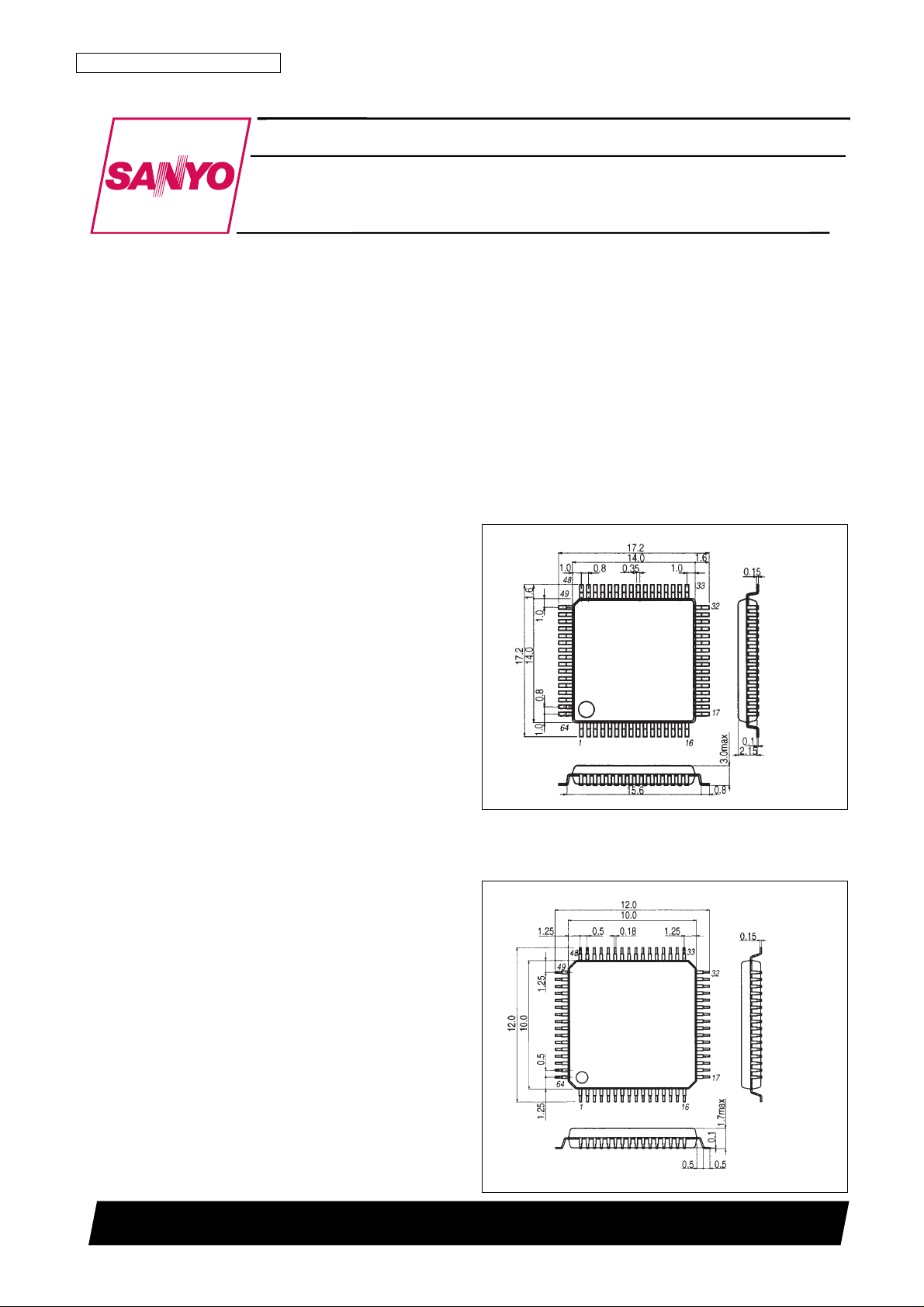
Package Dimensions
unit: mm
3159-QFP64G
unit: mm
3159-SQFP64
CMOS IC
31398RM (OT) No. 5799-1/12
Preliminary
SANYO: QFP64G
[LC72341G, 72342G, 72343G]
SANYO: SQFP64
[LC72341W, 72342W, 72343W]
SANYO Electric Co.,Ltd. Semiconductor Bussiness Headquarters
TOKYO OFFICE Tokyo Bldg., 1-10, 1 Chome, Ueno, Taito-ku, TOKYO, 110-8534 JAPAN
Low-Voltage Single-Chip Microcontrollers with On-
Chip PLL and LCD Driver Circuits
LC72341G/W, LC72342G/W, LC72343G/W
Ordering number : EN*5799
• IF counter
— HCTR input pin; 0.4 to 12 MHz
• Voltage detection circuit (VSENSE)
— Detects the VDDvoltage and sets a flag
• External reset pin
— Restarts execution from location 0 when the CPU and PLL circuits are operating
• Power on reset circuit
— Starts execution from location 0 at power on.
• Universal counter
— 20 bits
• Beep tones
— 3.1 and 1.5 kHz
• Halt mode: The microcontroller operating clock is stopped
• Backup mode: The crystal oscillator is stopped
• An amplifier for a low-pass filter is built in
• CPU and PLL circuit operating voltage
— 1.8 to 3.6 V
• RAM data retention voltage
— 1.0 V or higher
• Packages
— QIP-64G : 0.8-mm lead pitch
— SQFP-64 : 0.5-mm lead pitch
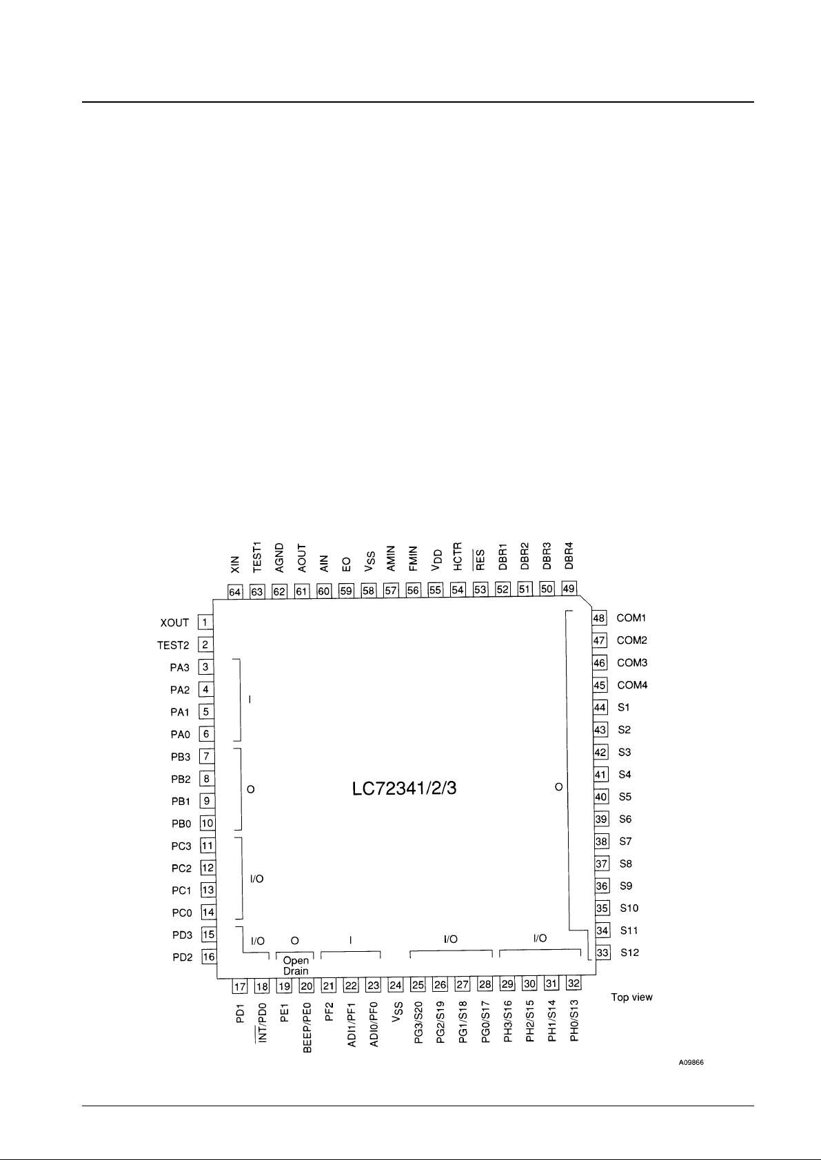
Pin Assignment
No. 5799-2/12
LC72341G/W, 72342G/W, 72343G/W
* PE0 and PE1 are open-drain outputs.
* The I/O ports can be set to input or output individually.
* The functions of the segment/general-purpose ports can be set in bit units.
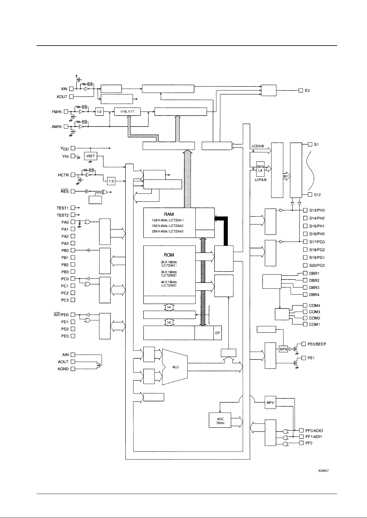
Block Diagram
No. 5799-3/12
LC72341G/W, 72342G/W, 72343G/W
Divider
Programmable divider
PLL data latch
PLL control
count end
Reference divider
Phase-
detector
System clock
generator
Time base
control
Pon
reset
Bus
driver
Data
latch/
Bus
driver
Data
latch/
Bus
driver
Address decoder
Program counter
Stack
Timer 0
Judge
Beep tone
Latch
A
Latch
B
JMP CAL
Return
interrupt
reset
Doubler
circuit
Common
driver
Instruction
decoder
Bus
control
Address
decoder
LCD
Port
driver
Lach
Bank
Skip
Bank
Data
latch/
Bus
driver
Data
latch/
Bus
driver
Data
latch/
Bus
driver
Data
latch/
Bus
driver
Data
latch/
Bus
driver
Universal counter
(20 bits)
Data bus
No. 5799-4/12
LC72341G/W, 72342G/W, 72343G/W
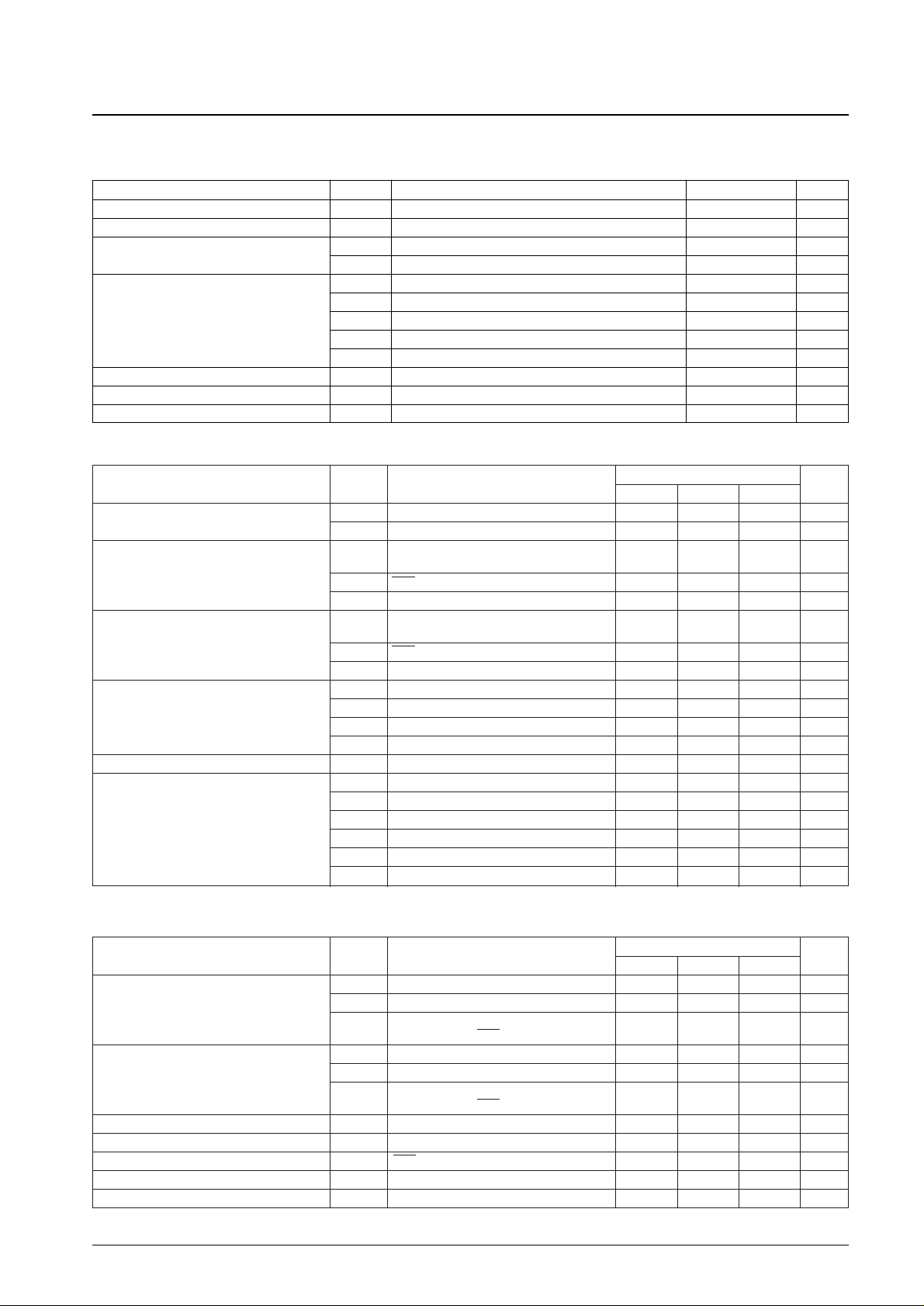
Parameter Symbol Conditions Ratings Unit
Maximum supply voltage V
DD
max –0.3 to +4.0 V
Input voltage V
IN
All input pins –0.3 to VDD+ 0.3 V
Output voltage
V
OUT
1 AOUT, PE –0.3 to +15 V
V
OUT
2 All output pins except V
OUT
1 –0.3 to VDDto + 0.3 V
I
OUT
1 PC, PD, PG, PH, EO 0 to 3 mA
I
OUT
2 PB 0 to 1 mA
Output current I
OUT
3 AOUT, PE 0 to 2 mA
I
OUT
4 S1 to S20 300 µA
I
OUT
5 COM1 to COM4 3 mA
Allowable power dissipation Pd max Ta = –20 to +70°C 300 mW
Operating temperature Topr –20 to +70 °C
Storage temperature Tstg –45 to +125 °C
Specifications
Absolute Maximum Ratings at Ta = 25°C, VSS= 0 V
Parameter Symbol Conditions
Ratings
Unit
min typ max
Supply voltage
V
DD
1 CPU and PLL operating voltage 1.8 3.0 3.6 V
V
DD
2 Memory retention voltage 1.0 V
V
IH
1
V
IH
2, VIH3, AMIN, FMIN,
0.7 V
DD
V
DD
V
Input high-level voltage
Input ports except HCTR and XIN.
V
IH
2 RES 0.8 V
DD
V
DD
V
V
IH
3 Port PF 0.6 V
DD
V
DD
V
V
IL
1
V
IL
2, VIL3, AMIN, FMIN,
0 0.3 V
DD
V
Input low-level voltage
Input ports except HCTR and XIN.
V
IL
2 RES 0 0.2 V
DD
V
V
IL
3 Port PF 0 0.2 V
DD
V
V
IN
1 XIN 0.5 0.6 Vrms
Input amplitude
V
IN
2 FMIN, AMIN 0.035 0.35 Vrms
V
IN
3 FMIN 0.05 0.35 Vrms
V
IN
4 HCTR 0.035 0.35 Vrms
Input voltage range V
IN
5 ADI0, ADI1 0 V
DD
V
F
IN
1 XIN : CI ≤ 35 kΩ 70 75 80 kHz
F
IN
2 FMIN : VIN2, VDD1 10 130 MHz
Input frequency
F
IN
3 FMIN : VIN3, VDD1 130 250 MHz
F
IN
4 AMIN (H) : VIN2, VDD1 2 40 MHz
F
IN
5 AMIN (L) : VIN2, VDD1 0.5 10 MHz
F
IN
6 HCTR : VIN4, VDD1 0.4 12 MHz
Allowable Operating Ranges at Ta = –20 to 70°C, VDD= 1.8 to 3.6 V
Parameter Symbol Conditions
Ratings
Unit
min typ max
I
IH
1 XIN: VI= VDD= 3.0 V 3 µA
Input high-level current
I
IH
2 FMIN, AMIN, HCTR : VI= VDD= 3.0 V 3 8 20 µA
I
IH
3
Ports PA/PF (with no pull-down resistor), PC,
3 µA
PD, PG, and PH. RES: V
I
= VDD= 3.0 V
I
IL
1 XIN : VI= VDD= V
SS
–3 µA
Input low-level current
I
IL
2 FMIN, AMIN, HCTR : VI= VDD= V
SS
–3 –8 –20 µA
I
IL
3
Ports PA/PF (with no pull-down resistor), PC,
–3 µA
PD, PG, and PH. RES: V
I
= VDD= V
SS
Input floating voltage V
IF
PA/PF with pull-down resistors used 0.05 V
DD
V
Pull-down resistance R
PD
1
PA/PF with pull-down resistors used, VDD= 3 V
75 100 200 kΩ
Hysteresis V
H
RES 0.1 V
DD
0.2 V
DD
V
Voltage doubler reference voltage DBR4 Ta = 25°C, referenced to V
DD
, C3 = 0.47 µF 1.3 1.5 1.7 V
Voltage doubler step-up voltage DBR1, 2, 3
Ta = 25°C, C1 = 0.45 µF, C2 = 0.47 µF, no load
2.7 3.0 3.3 V
Electrical Characteristics at Ta = –20 to 70°C, VDD= 1.8 to 3.6 V (in the allowable operating ranges)
 Loading...