

SANYO LC72323-XXXX Datasheet
Overview
The LC72323-XXXX is a single-chip car audio system
electronic tuning controller that supports detachable
function block systems. This product supports reception in
all areas of the world and include PLL, LCD driver and
electronic volume/tone control support circuits on chip.
Features
• Support for reception of the European FM, MW and LW
bands and the FM and AM bands used in the US,
Australia, the Middle and Near East and South America
• Support for electronic volume/tone controls (bass,
treble, balance and fader) using the LC75371M
• VF seek and auto retune functions (Europe)
• Support for IF counting techniques in all bands
• Automatic memory function in station strength order
(FM band)
• Loudness control
• CD functions
— Key inputs
— CD indicator display function
• Tape functions
— Tape indicator display function
— Dolby, APSS and metal tape controls
• Clock function with 24-hour display for Europe and
12-hour display for other reception areas
• Single 5 V power supply
• Package: QFP80E (QIP80E)
• Telephone mute function
• LED blinking function
Package Dimensions
unit: mm
3174-QFP80E
CMOS LSI
13097HA (OT)/73195TH (OT) No. 4934-1/27
Preliminary
SANYO: QIP80E
[LC72323-XXXX]
SANYO Electric Co.,Ltd. Semiconductor Bussiness Headquarters
TOKYO OFFICE Tokyo Bldg., 1-10, 1 Chome, Ueno, Taito-ku, TOKYO, 110 JAPAN
Provisional Development Specifications
LC72323-XXXX
Ordering number : *EN4934A
This LSI can easily use CCB that is SANYO’s original bus format.
• CCB is a trademark of SANYO ELECTRIC CO., LTD.
• CCB is SANYO’s original bus format and all the bus
addresses are controlled by SANYO.
No. 4934-2/27
LC72323-XXXX
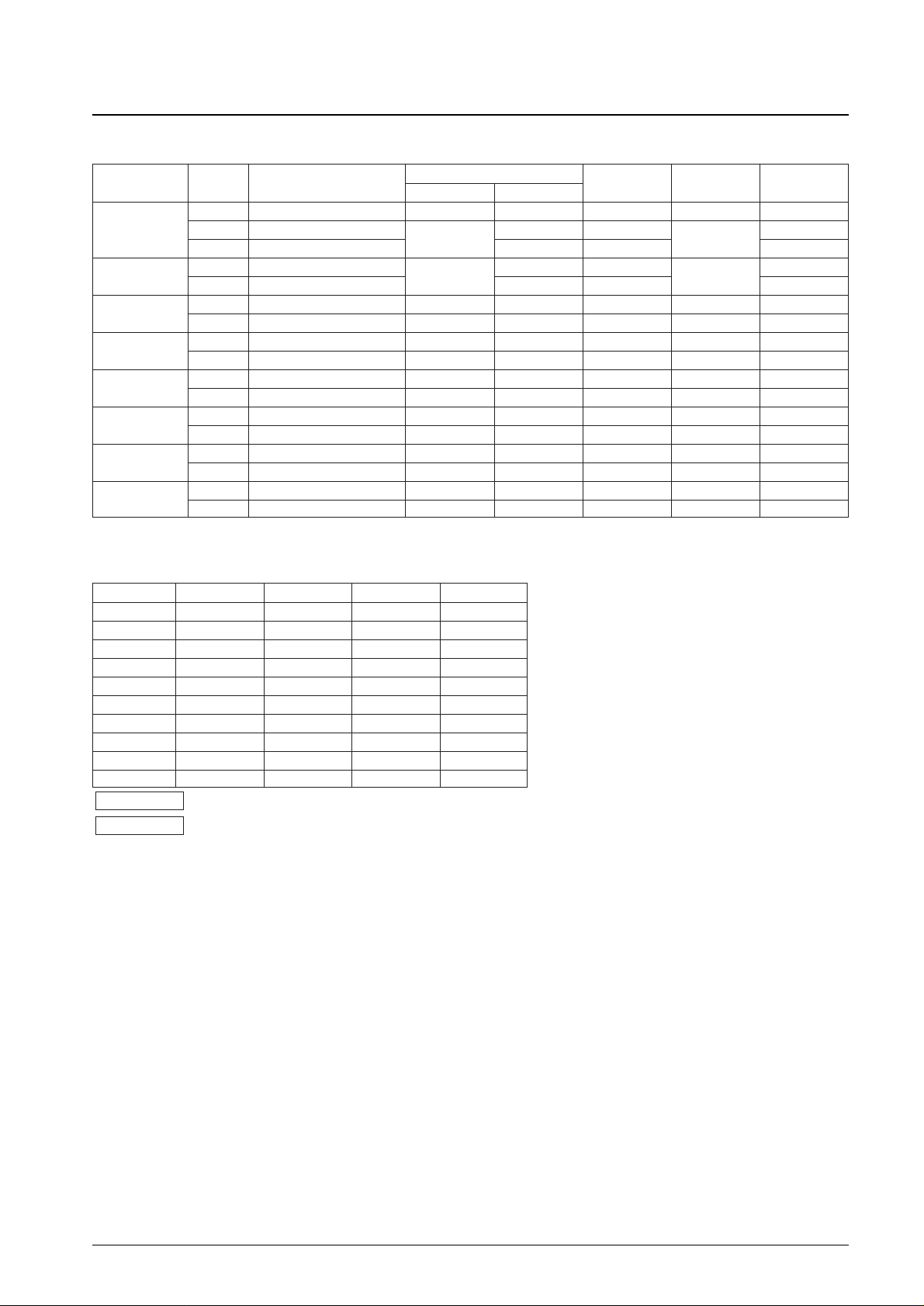
Parameter Symbol Conditions Ratings Unit
Maximum supply voltage V
DD
max –0.3 to +6.5 V
Input voltage
V
IN
(1) HOLD, TELIN, RES, SNS, ADI, SD, ST, SK, DK –0.3 to +13 V
V
IN
(2) Inputs other than VIN(1) –0.3 to VDD+ 0.3 V
Output voltage
V
OUT
(1) BEEP, BAND2, BAND1, POWER –0.3 to +15 V
V
OUT
(2) Outputs other than V
OUT
(1) –0.3 to VDD+ 0.3 V
I
OUT
(1)
AMUTE, LEDFL, DI/KS9, CLK/KS8, BEEP, BAND2,
0 to 5 mA
Output current
BAND1, POWER
I
OUT
(2) DOLBY, METAL, APSS, LOUDNESS, LOCAL, STEREO 0 to 3 mA
I
OUT
(3) KS0, KS1, KS2, KS3, KS4, KS5, KS6, CE/KS7 0 to 1 mA
Allowable power dissipation Pd max Ta = –40 to +85°C 300* mW
Operating temperature Topr –40 to +85 °C
Storage temperature Tstg –45 to +125 °C
Specifications
Absolute Maximum Ratings at Ta = 25°C, VSS= 0 V
Note: * Reference value
Parameter Symbol Conditions
Ratings
Unit
min typ max
V
DD
(1) With the CPU and PLL operating 4.5 5.5 V
Supply voltage V
DD
(2) CPU operating 3.5 5.5 V
V
DD
(3) Memory retention 1.3 5.5 V
V
IH
(1) SK, DK, SD, ST 0.7 V
DD
8.0 V
V
IH
(2) RES, INT, HOLD 0.8 V
DD
8.0 V
Input high level voltage V
IH
(3) SNS 2.5 8.0 V
V
IH
(4) K0, K1, K2, K3 0.6 V
DD
V
DD
V
V
IH
(5) TAPE, TAPERUN 0.7 V
DD
V
DD
V
V
IL
(1) SK, DK, SD, ST 0 0.3 V
DD
V
V
IL
(2) RES, INT 0 0.2 V
DD
V
Input low level voltage
V
IL
(3) SNS 0 1.3 V
V
IL
(4) K0, K1, K2, K3 0 0.2 V
DD
V
V
IL
(5) TAPE, TAPERUN 0 0.3 V
DD
V
V
IL
(6) HOLD 0 0.4 V
DD
V
F
IN
(1) XIN 4.0 4.5 5.0 MHz
F
IN
(2) FM OSC, VIN(2), VDD(1) 10 130 MHz
Input frequency F
IN
(3) AM OSC, VIN(3), VDD(1) 0.5 10 MHz
F
IN
(4) FMIF, VIN(4), VDD(1) 0.4 12 MHz
F
IN
(5) AMIF, VIN(4), VDD(1) 100 500 kHz
V
IN
(1) XIN 0.50 1.5 Vrms
Input amplitude
V
IN
(2) FM OSC 0.10 1.5 Vrms
V
IN
(3) AM OSC 0.10 1.5 Vrms
V
IN
(4) FMIF, AMIF 0.10 1.5 Vrms
Input voltage range V
IN
(5) ADI 0 V
DD
V
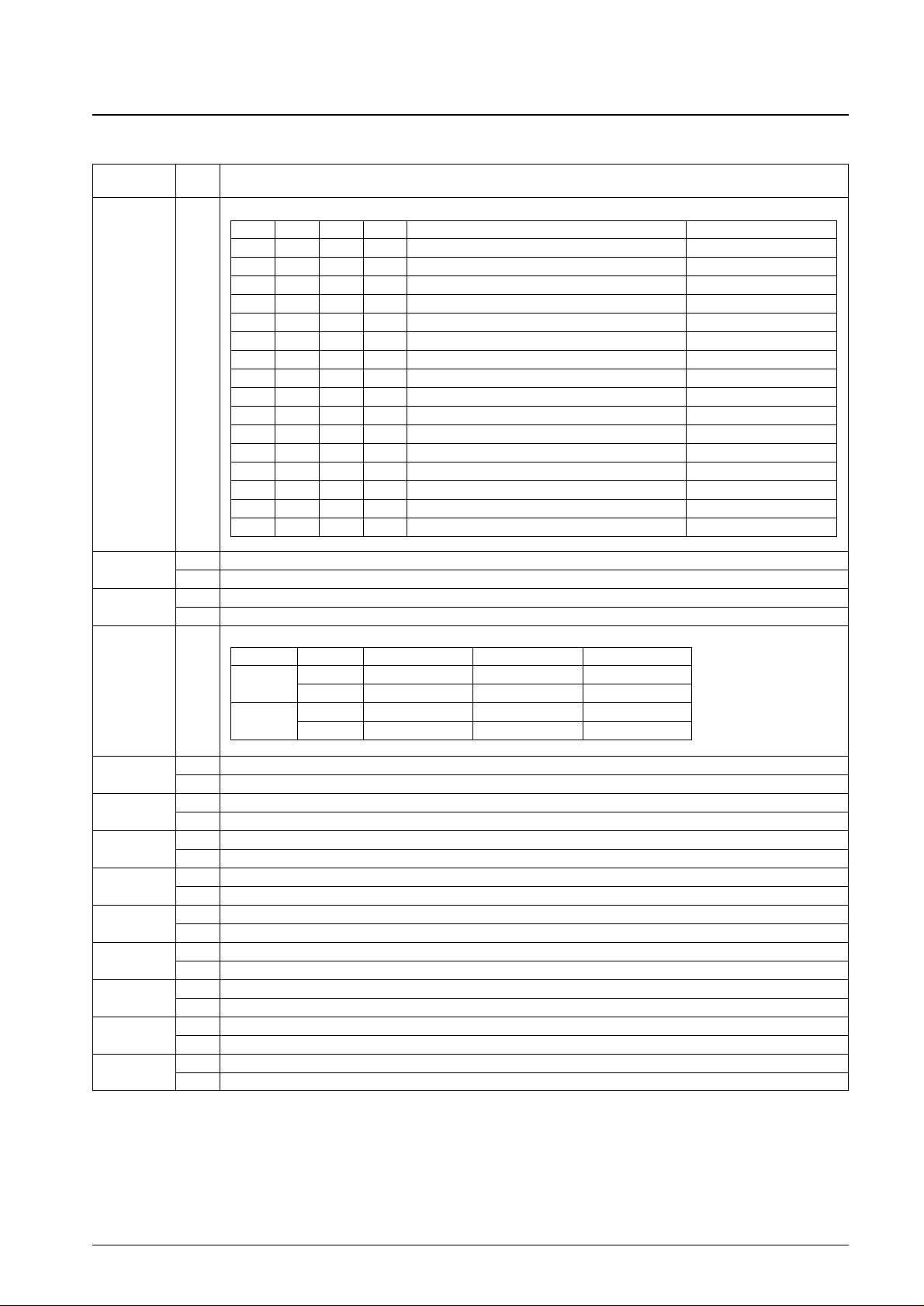
Allowable Operating Ranges at Ta = –40 to +85°C, VDD= 3.5 to 5.5 V

No. 4934-3/27
LC72323-XXXX
Parameter Symbol Conditions
Ratings
Unit
min typ max
Power down detection voltage VDET 2.7 3.0 3.3 V
IIH(1)
TELIN, HOLD, RES, ADI, SNS, SK, DK, SD, ST:
3.0 µA
V
I
= 5.5 V
Input high level current
I
IH
(2) XIN: VI= VDD= 5.0 V 2.0 5.0 15 µA
I
IH
(3) FM OSC, AM OSC, FMIF, AMIF: VI= VDD= 5.0 V 4.0 10 30 µA
I
IH
(4) K0, K1, K2, K3: VI= VDD= 5.0 V 50 µA
I
IH
(5) TAPE, TAPERUN: VI= V
DD
3.0 µA
I
IL
(1)
TELIN, HOLD, RES, ADI, SNS, SK, DK, SD, ST:
3.0 µA
V
I
= V
SS
Input low level current
I
IL
(2) XIN: VI= V
SS
2.0 5.0 15 µA
I
IL
(3) FM OSC, AM OSC, FMIF, AMIF: VI= V
SS
4.0 10 30 µA
I
IL
(4) TAPE, TAPERUN: VI= V
SS
3.0 µA
Input floating voltage VIF K0, K1, K2, K3 0.05 V
DD
V
Pull-down resistance RPD K0, K1, K2, K3: V
DD
= 5 V 75 100 200 kΩ
I
OFFH
(1) EO1, EO2: VO= V
DD
0.01 10 nA
KS0 to KS6, CE/KS7, CLK/KS8, DI/KS9, LEDFL,
Output off leakage current
I
OFFH
(2) AMUTE, LOUDNESS, APSS, METAL, DOLBY, 3.0 µA
STEREO, LOCAL: V
O
= V
DD
I
OFFH
(3) BAND1, BAND2, BEEP, POWER: VO= 13 V 5.0 µA
I
OFFL
(1) EO1, EO2: VO= V
SS
0.01 10 nA
Output off leakage current
KS0 to KS6, CE/KS7, CLK/KS8, DI/KS9, LEDFL,
I
OFFL
(2) AMUTE, LOUDNESS, APSS, METAL, DOLBY, 3.0 µA
STEREO, LOCAL: V
O
= V
SS
VOH(1) KS0 to KS6, CE/KS7: IO= 1 mA VDD– 2.0 VDD– 1.0 VDD– 0.5 V
V
OH
(2)
LOUDNESS, APSS, METAL, DOLBY, STEREO,
VDD– 1.0 V
LOCAL: I
O
= 1 mA
Output high level voltage
V
OH
(3) EO1, EO2: IO= 500 µA VDD– 1.0 V
V
OH
(4) XOUT: IO= 200 µA VDD– 1.0 V
V
OH
(5) S1 to S28: IO= 0.1 mA VDD– 1.0 V
V
OH
(6) COM1, COM2: IO= 25 µA VDD– 0.75 VDD– 0.5 VDD– 0.3 V
V
OH
(7) AMUTE, LEDFL, CLK/KS8, DI/KS9: IO= 5 mA VDD– 1.0 V
V
OL
(1) KS0 to KS6, CE/KS7: IO= 50 µA 0.5 1.0 2.0 V
V
OL
(2)
LOUDNESS, APSS, METAL, DOLBY, STEREO,
1.0 V
LOCAL: I
O
= 1 mA
V
OL
(3) EO1, EO2: IO= 500 µA 1.0 V
Output low level voltage
V
OL
(4) XOUT: IO= 200 µA 1.0 V
V
OL
(5) S1 to S28: IO= 0.1 mA 1.0 V
V
OL
(6) AMUTE, LEDFL, CLK/KS8, DI/KS9: IO= 5 mA 1.0 V
V
OL
(7) COM1, COM2: IO= 25 µA 0.3 0.5 0.75 V
V
OL
(8) BAND1, BAND2, BEEP, POWER: IO= 5 mA
0.75 2.0
V
(150 Ω) (400 Ω)
Output mid-level voltage VM COM1, COM2, V
DD
= 5 V, IO= 20 µA 2.0 2.5 3.0 V
I
DD
(1) VDD(1), FIN(2) = 130 MHz 15 20 mA
I
DD
(2) VDD(2), PLL stopped, (hold mode, Figure 1) 1.0 mA
Current drain
I
DD
(3)
V
DD
= 5.5 V, oscillator stopped, Ta = 25°C
5 µA
(backup mode, Figure 2)
I
DD
(4)
V
DD
= 2.5 V, oscillator stopped, Ta = 25°C
1 µA
(backup mode, Figure 2)
Electrical Characteristics for the Allowable Operating Ranges
*1: K0, K1, K2, K3, TAPE, TAPERUN
Note: BEEP, BAND2, BAND1, POWER, LOCAL, STEREO, DOLBY, METAL, APSS, LOUDNESS, AMUTE, LEDFL, DI/KS9, CLK/KS8, CE/KS7, KS0 to KS6
= “Open”
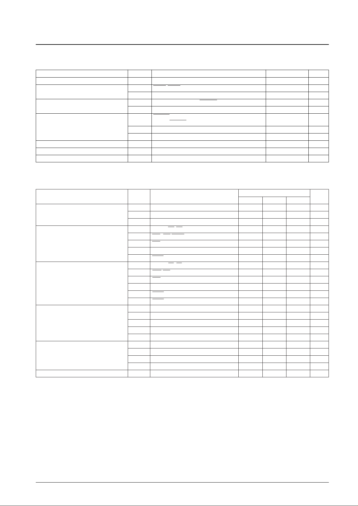
Figure 1 IDD(2) in Hold Mode
Note: With all ports other than those specifically mentioned left open
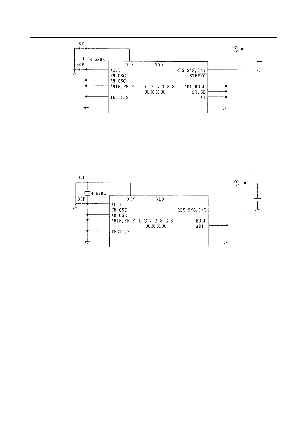
Figure 2 IDD(3) in Backup Mode
No. 4934-4/27
LC72323-XXXX
Unit (capacitance: F)
Unit (capacitance: F)
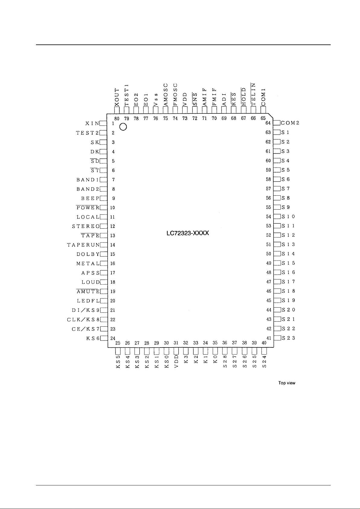
Pin Assignment
No. 4934-5/27
LC72323-XXXX
No. 4934-6/27
LC72323-XXXX
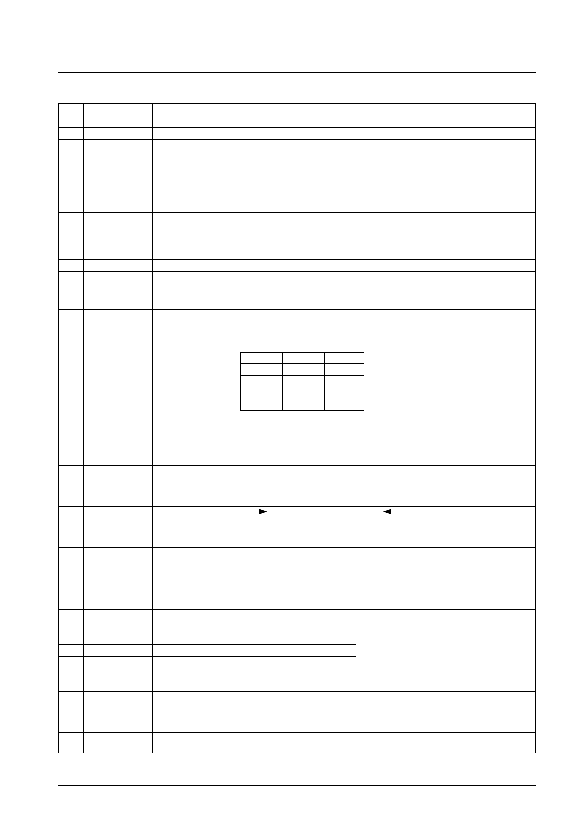
Reception Frequencies
Key and Diode Matrix
⇒ Tact switch
⇒ Diode switch
▲
Area Band Reciving frequency
Channel spacing
Reference
IF
IF count
Auto Manual
frequency tolerance
FM 87.5 – 108.0 MHz 50 kHz 50 kHz 25 kHz 10.7 MHz ±10 kHz
Europe 1 MW 531 – 1602 kHz
9 kHz
9 kHz 9 kHz
459 kHz
±3 kHz
LW 153 – 281 kHz 1 kHz 1 kHz ±0.6 kHz
Europe 2
MW 531 – 1602 kHz
9 kHz
9 kHz 9 kHz
459 kHz
±3 kHz
LW 153 – 281 kHz 1 kHz 1 kHz ±0.6 kHz
Europe 3
FM 87.5 – 108.0 MHz 50 kHz 50 kHz 25 kHz 10.7 MHz ±10 kHz
AM 531 – 1602 kHz 9 kHz 9 kHz 9 kHz 459 kHz ±3 kHz
USA 1
FM 87.9 – 107.9 MHz 200 kHz 200 kHz 25 kHz 10.7 MHz ±10 kHz
AM 530 – 1710 kHz 10 kHz 10 kHz 10 kHz 450 kHz ±3 kHz
USA 2
FM 87.9 – 107.9 MHz 200 kHz 200 kHz 25 kHz 10.7 MHz ±10 kHz
AM 530 – 1710 kHz 10 kHz 10 kHz 10 kHz 450 kHz ±3 kHz
Middle east/
FM 87.9 – 107.9 MHz 100 kHz 100 kHz 25 kHz 10.7 MHz ±10 kHz
Australia 1
AM 531 – 1602 kHz 9 kHz 9 kHz 9 kHz 450 kHz ±3 kHz
Middle east/
/ FM 87.9 – 107.9 MHz 100 kHz 100 kHz 25 kHz 10.7 MHz ±10 kHz
Australia 2
AM 531 – 1602 kHz 9 kHz 9 kHz 9 kHz 450 kHz ±3 kHz
South America
FM 87.5 – 108.0 MHz 100 kHz 100 kHz 25 kHz 10.7 MHz ±10 kHz
AM 520 – 1620 kHz 10 kHz 10 kHz 10 kHz 450 kHz ±3 kHz
K3 K2 K1 K0
KS0 MAN UP/T UP MAN DN/T DN STEREO DISP
KS1 SEEK UP SEEK DOWN SCAN UP PS/AMEM
KS2 M1 M2 M3 M4/METAL
KS3 M5/DOLBY M6/APSS VF BAND
KS4 V UP V DOWN LOUDNESS LOCAL
KS5 CD MODE MUTE POWER
KS6 AREA0 ▲ AREA1 ▲ AREA2 ▲ AREA3 ▲
KS7 COLON ▲ CD SEL ▲ DF SEL ▲ AUTO500 ▲
KS8 CLOCK ▲ IF0 ▲ PRIORITY ▲ FADER ▲
KS9 VR SEL ▲ POWSEL ▲ LEDSEL ▲ POWAMP ▲
No. 4934-7/27
LC72323-XXXX
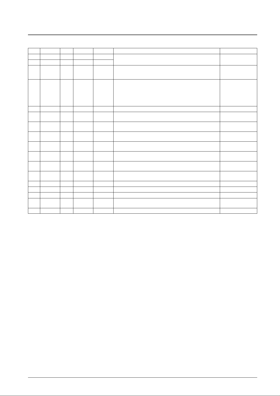
Diode Switches
Diode matrix On/
Function
name off
These diodes set the target reception area. The target reception area and bands are determined by the following combinations.
COLON
0 Clock colon display selection set to always on.
1 Clock colon display selection set to blink at a1 Hz rate.
CD SEL
0 No CD function
1 CD function enabled
Double function key selection
DF SEL
AUTO500
0 The MAN UP/T UP and MAN DN/T DN key functions as the MAN UP/DN key
1 The MAN UP/T UP and MAN DN/T DN key functions as the T UP/DN key
CLOCK
0 Clock function enabled (24-hour display in Europe, 12-hour display in other reception areas)
1 No clock
IF0
0 Auto stop on SD only
1 Auto stop on SD and IF count
PRIORITY
0 Clock display takes priority
1 Frequency, tape and CD displays take priority
FADER
0 Fader function enabled
1 No fader function
VR SEL
0 Electronic volume/tone control functions enabled
1 No electronic volume/tone control functions
POWSEL
0 The power key turns the power on or off.
1 The HOLD pin turns the power on or off.
LEDSEL
0 LEDs flash when /HOLD is low.
1 LEDs do not flash when /HOLD is low.
POWAMP
0 The LC75371M input gain control data outputs +18 dB.
1 The LC75371M input gain control data outputs 0 dB.
AREA3 AREA2 AREA1 AREA0 Area Band
0 0 0 0 Europe 1 FM1/FM2/MW/LW
0 0 0 1 Europe 2 MW/LW
0 0 1 0 Europe 3 FM/AM
0 0 1 1 South America FM1/FM2/AM
0 1 0 0 USA 1 FM1/FM2/AM
0 1 0 1 USA 2 FM1/FM2/FM3/AM
0 1 1 0 Middle east/Australia 1 FM1/FM2/AM
0 1 1 1 Middle east/Australia 2 FM1/FM2/FM3/AM
1 0 0 0 Europe 1 FM1/FM2/FM3
1 0 0 1 Europe 3 FM
1 0 1 0 Europe 3 FM1/FM2/FM3/AM
1 0 1 1 South America FM1/FM2/FM3/AM
1 1 0 0 USA 1 FM1/FM2
1 1 0 1 USA 2 FM
1 1 1 0 Middle east/Australia 1 FM1/FM2
1 1 1 1 Middle east/Australia 2 FM
DFSEL Mode M4/METAL M5/DOLBY M6/APSS
0
RADIO M4 M5 M6
TAPE METAL DOLBY APSS
1
RADIO M4 M5 M6
TAPE — — —
AREA0
AREA1
AREA2
AREA3
No. 4934-8/27
LC72323-XXXX
Ports
Note: * See the item on double function key beep output.
Pin Name I/O Allocation Active Function Handling when unused
1 XIN I XIN — —
2 TEST2 I TEST2 — —
3 PG3 I SK H
Connect directly to
ground.
Connect directly to
4 PG2 I DK H
ground.
5 PG1 I /SD L Must be used.
6 PG0 I /ST L
Connect directly to
V
DD
.
7 PH3 O BEEP H Open
8 PH2 O BAND2 H Open
9 PH1 O BAND1 H Open
10 PH0 O /POWER L
Connect directly to
ground.
11 PF3 O LOCAL H Open
12 PF2 O STEREO H Open
13 PF1 I /TAPE L
Connect directly to
V
DD
.
14 PF0 I TAPE RUN —
Connect directly to
ground.
15 PE3 O DOLBY H Open
16 PE2 O METAL H Open
17 PE1 O APSS H Open
18 PE0 O LOUDNESS H Open
19 PD3 O /AMUTE L Open
20 PD2 O LEDFL H Open
21 PD1 O DI/KS9 H
22 PD0 O CLK/KS8 H
23 PC3 O CE/KS7 H Open
24 PC2 O KS6 H
25 PC1 O KS5 H
26 to PC0 to
O KS4 to KS0 H
Open
30 PB0
32 to PA3 to
I K3 to K0 H
Connect directly to
35 PA0 ground.
36 to S28 to
O
S28 to
H Open
63 S1 S1
Connection for the 4.5 MHz crystal
Connect to ground
High: “SK” display on, low: “SK” display off
In bands other than the FM band, the SK display is always off
regardless of whether this pin is high or low.
An SK high search starts when the VF key is pressed. When an SD
present state is detected, the circuit checks again after between 375
and 500 ms, and if the signal is high, it holds that frequency. After
that, if a low level continues for 25 seconds, an auto retune operation
starts. (sampling = 25 ms)
In VF mode and in either tape or CD mode, if a high level is input to
this signal (if a high level is detected three times in a row at 25 ms
intervals), the circuit switches to radio mode, and ARI broadcast
reception becomes possible. Also, after a VF key on and an SK seek,
DK is checked 2 s after an SK present state is recognized.
Output signal that reports station reception during auto tuning.
Low: “STEREO” display on, high: “STEREO” display off
the STEREO display is turned off in bands other than the FM band
regardless of the high or low state of this pin.
Monitors all keys and outputs a 50 ms 3 kHz pulse when any key is
pressed. (A pull-up resistor is required.)*
These pin outputs change according to the table when either the
BAND or VF key is pressed. (A pulll-up resistor is required.)
Outputs a low level in power on mode, high in power off mode.
(A pull-up resistor is required.)
Outputs a low level in normal mode. Outputs a high level when the
DX display is turned off in seek and scan modes.
The output is inverted when the stereo key is pressed in the FM band.
Detects a tape input.
The “ ” indicator lights when high and the “ ” indicator lights
when low.
High indicates that the Dolby indicator is on (only in tape mode) and a
low indicates that the Dolby indicator is off.
High indicates that the metal indicator is on (only in tape mode) and a
low indicates that the metal indicator is off.
High indicates that the “APSS” indicator is on (only in tape mode) and
a low indicates that the “APSS” indicator is off.
High indicates that the loudness indicator is on and a low indicates
that the loudness indicator is off.
Audio mute output
The LEDs flash when /HOLD is low. (When LEDSEL is 0.)
Connect to the LC75371M DI pin.
Connect to the LC75371M CLK pin.
Connect to the LC75371M CE pin. Diode matrix source output
Key matrix source output
Key & diode matrix return input
LCD segment output
BAND1 BAND2
VF H H
FM H L
MW L L
LW L H
Continued on next page.
No. 4934-9/27
LC72323-XXXX
Continued from preceding page.
Pin Name I/O Allocation Active Function Handling when unused
64 COM2 O COM2 H
Open
65 COM1 O COM1 H
Connect directly to
66 /INT I /TELIN L
V
DD
.
67 /HOLD I /HOLD L —
68 /RES I /RES L —
69 ADI I ADI —
Connect directly to
ground.
70 HCTR I FMIF —
Connect directly to
ground.
71 LCTR I AMIF —
Connect directly to
ground.
72 /SNS I /SNS L
Connect directly to
V
DD
.
73 V
DD
I V
DD
—
Connect directly to
Connect to +5 V.
V
DD
.
74 FMIN I FM OSC —
Connect directly to
ground.
75 AMIN I AM OSC —
Connect directly to
ground.
76 V
SS
I V
SS
— —
77 EO1 O EO1 — Open
78 EO2 O EO2 — Open
79 TEST1 I TEST1 —
Connect directly to
ground.
80 XOUT O XOUT — Connection for the 4.5 MHz crystal —
LCD common output
When this pin is set low, “TEL” is displayed and the /AMUTE pin is set
low. When PRIORITY is 0, “TEL” is displayed for 5 seconds and then
the display returns to the clock display.
Used for detecting the power on/off state.
When /HOLD goes low
• If the clock function is enabled:
The clock count function operates without stopping the oscillator.
• If the clock function is disabled:
The oscillator is stopped and the chip goes to the power save mode.
Connect to V
DD
.
Connect to the S METER pin. (max = 3.2 V)
Inputs the FM IF signal.
Inputs the AM IF signal.
Used for power supply detection.
FM local oscillator input
AM local oscillator input
Connect to ground.
Phase comparator output
Phase comparator output
Connect to ground.
 Loading...