

CMOS LSI
Ordering number : EN5378
93096HA (OT) No. 5378-1/13
SANYO Electric Co.,Ltd. Semiconductor Bussiness Headquarters
TOKYO OFFICE Tokyo Bldg., 1-10, 1 Chome, Ueno, Taito-ku, TOKYO, 110 JAPAN
Single-Chip Microcontroller with PLL
and LCD Driver
LC72322R, 72323R
Overview
The LC72322R and LC72323R are single-chip
microcontrollers for use in electronic tuning applications.
These ICs include on chip both LCD drivers and a PLL
circuit that can operate at up to 150 MHz. The LC72322R
and LC72323R feature that these ICs are reversed pinassignment versions of LC72322 and LC72323
respectively and have the equal functions and
specifications to theirs respectively.
Functions
• Stack: Eight levels
• Fast programmable divider
• General-purpose counters: HCTR for frequency
measurement and LCTR for frequency or period
measurement
• LCD driver for displays with up to 56 segments
(1/2 duty, 1/2 bias)
• Program memory (ROM):4095 (8 KB) 16-bit digits:
LC72322R
3071 (6 KB) 16-bit digits:
LC72323R
• Data memory (RAM): 256 4-bit digits
• All instructions are single-word instructions
• Cycle time: 2.67 µs, 13.33 µs, or 40.00 µs (option)
• Unlock FF: 0.55 µs detection, 1.1 µs detection
• Timer FF: 1 ms, 5ms, 25ms, 125ms
• Input ports*: One dedicated key input port and one
high-breakdown voltage port
• Output ports*: Two dedicated key output ports, one
high-breakdown voltage open-drain port
Two CMOS output ports (of which one
can be switched to be used as LCD driver
outputs)
Seven CMOS output ports (mask option
switchable to use as LCD ports)
• I/O ports*: One switchable between input and output
in four-bit units and one switchable
between input and output in bit units
Note: * Each port consists of four bits.
• Program runaway can be detected and a special address
set (Programmable watchdog timer).
• Voltage detection type reset circuit
• One 6-bit A/D converter
• Two 8-bit D/A converters (PWM): LC72322R only
• One external interrupt
• Hold mode for RAM backup
• Sense FF for hot/cold startup determination
• PLL: 4.5 to 5.5 V
• CPU: 3.5 to 5.5 V
• RAM: 1.3 to 5.5 V
• LC72P321R as OTP used
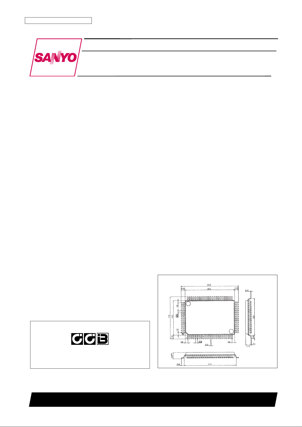
• Package: QIP80DR
Package Dimensions
unit: mm
3223-QFP80DR
This LSI can easily use CCB that is SANYO’s original bus format.
• CCB is a trademark of SANYO ELECTRIC CO., LTD.
• CCB is SANYO’s original bus format and all the bus
addresses are controlled by SANYO.
SANYO: QIP80DR
[LC72322R, LC72323R]
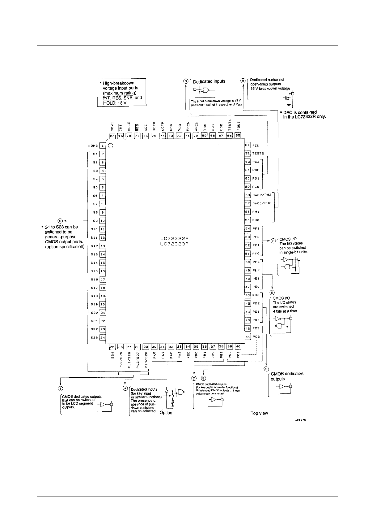
Pin Assignment
No. 5378-2/13
LC72322R, 72323R
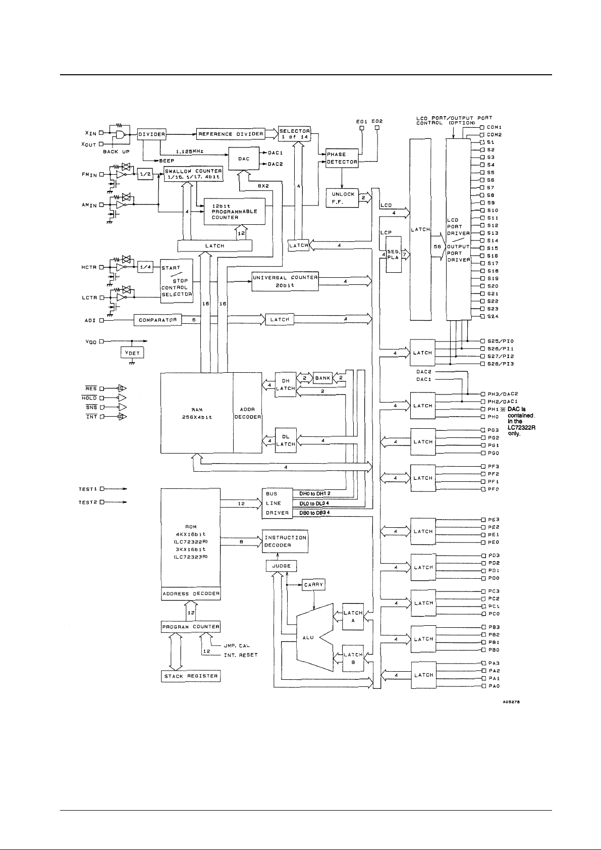
Block Diagram
No. 5378-3/13
LC72322R, 72323R
Specifications
Absolute Maximum Ratings at Ta = 25°C, VSS= 0 V
Allowable Operating Ranges at Ta = –40 to +85°C, VDD= 3.5 to 5.5 V
No. 5378-4/13
LC72322R, 72323R
Parameter Symbol Conditions Ratings Unit
Maximum supply voltage V
DD
max –0.3 to +6.5 V
Input voltage
V
IN
1 HOLD, INT, RES, ADI, SNS, and the G port –0.3 to +13 V
V
IN
2 Inputs other than VIN1 –0.3 to VDD+ 0.3 V
Output voltage
V
OUT
1 H port –0.3 to +15 V
V
OUT
2 Outputs other than V
OUT
1 –0.3 to VDD+ 0.3 V
I
OUT
1 All D and H port pins 0 to 5 mA
Output current
I
OUT
2 All E and F port pins 0 to 3 mA
I
OUT
3 All B and C port pins 0 to 1 mA
I
OUT
4 S1 to S28 and all I port pins 0 to 1 mA
Allowable power dissipation Pd max Ta = –40 to +85°C 300 mW
Operating temperature Topr –40 to +85 °C
Storage temperature Tstg –45 to +125 °C
Parameter Symbol Conditions
Ratings
Unit
min typ max
V
DD
1 CPU and PLL operating 4.5 5.5 V
Supply voltage V
DD
2 CPU operating 3.5 5.5 V
V
DD
3 Memory retention voltage 1.3 5.5 V
V
IH
1 G port 0.7 V
DD
8.0 V
V
IH
2 RES, INT, HOLD 0.8 V
DD
8.0 V
Input high level voltage
V
IH
3 SNS 2.5 8.0 V
V
IH
4 A port 0.6 V
DD
V
DD
V
V
IH
5 PE0, PE2 and F ports 0.7 V
DD
V
DD
V
V
IH
6
LCTR (period measurement),
0.8 V
DD
V
DD
V
V
DD
1, PE1 and PE3
V
IL
1 G port 0 0.3 V
DD
V
V
IL
2 RES, INT, PE1, PE3 0 0.2 V
DD
V
V
IL
3 SNS 0 1.3 V
Input low level voltage V
IL
4 A port 0 0.2 V
DD
V
V
IL
5 PE0, PE2 and F ports 0 0.3 V
DD
V
V
IL
6 LCTR (period measurement), VDD1 0 0.2 V
DD
V
V
IL
7 HOLD 0 0.4 V
DD
V
f
IN
1 XIN 4.0 4.5 5.0 MHz
f
IN
2 FMIN, VIN2, VDD1 10 130 MHz
f
IN
3 FMIN, VIN3, VDD1 10 150 MHz
Input frequency
f
IN
4 AMIN (L), VIN4, VDD1 0.5 10 MHz
f
IN
5 AMIN (H), VIN5, VDD1 2.0 40 MHz
f
IN
6 HCTR, VIN6, VDD1 0.4 12 MHz
f
IN
7 LCTR (frequency), VIN7, VDD1 100 500 kHz
f
IN
8 LCTR (period), VIH6, VIL6, VDD1 1 20 × 10
3
Hz
V
IN
1 XIN 0.50 1.5 Vrms
V
IN
2 FMIN 0.10 1.5 Vrms
Input amplitude V
IN
3 FMIN 0.15 1.5 Vrms
V
IN
4, 5 AMIN 0.10 1.5 Vrms
V
IN
6, 7 LCTR, HCTR 0.10 1.5 Vrms
Input voltage range V
IN
8 ADI 0 V
DD
V

Electrical Characteristics for the Allowable Operating Ranges
No. 5378-5/13
LC72322R, 72323R
Parameter Symbol Conditions
Ratings
Unit
min typ max
Hysteresis V
H
LCTR (period), RES, INT, PE1, PE3 0.1 V
DD
V
Rejected pulse width P
REJ
SNS 50 µs
Power-down detection voltage V
DET
2.7 3.0 3.3 V
I
IH
1
INT, HOLD, RES, ADI, SNS,
3.0 µA
and G port: V
I
= 5.5 V
I
IH
2
A, E, and F ports: E and F ports with
3.0 µA
Input high level current
outputs off, A port with no R
PD
, VI= V
DD
IIH3 XIN: VI= VDD= 5.0 V 2.0 5.0 15 µA
I
IH
4
FMIN, AMIN, HCTR, LCTR:
4.0 10 30 µA
V
I
= VDD= 5.0 V
I
IH
5 A port: With an RPD, VI= VDD= 5.0 V 50 µA
I
IL
1
INT, HOLD, RES, ADI, SNS,
3.0 µA
and the G port: V
I
= V
SS
Input low level current
I
IL
2
A, E, and F ports: E and F ports with
3.0 µA
outputs off, A port with no R
PD
, VI= V
SS
IIL3 XIN: VIN= V
SS
2.0 5.0 15 µA
I
IL
4 FMIN, AMIN, HCTR, LCTR: VI= V
SS
4.0 10 30 µA
Input floating voltage V
IF
A port: With an R
PD
0.05 V
DD
V
Pull-down resistance R
PD
A port: With an RPD, VDD= 5.0 V 75 100 200 kΩ
I
OFFH
1 EO1, EO2: VO= V
DD
0.01 10 nA
Output high level off leakage current I
OFFH
2 B, C, D, E, F, and I ports: VO= V
DD
3.0 µA
I
OFFH
3 H port: VO= V
DD
5.0 µA
Output low level off leakage current
I
OFFL
1 EO1, EO2: VO= V
SS
0.01 10 nA
I
OFFL
2 B, C, D, E, F, and I ports: VO= V
SS
3.0 µA
V
OH
1 B and C ports: IO= 1 mA VDD– 2.0 VDD– 1.0 VDD– 0.5 V
V
OH
2 E and F ports: IO= 1 mA VDD– 1.0 V
V
OH
3 EO1, EO2: IO= 500 µA VDD– 1.0 V
Output high level voltage V
OH
4 XOUT: IO= 200 µA VDD– 1.0 V
V
OH
5 S1 to S28 and the I port: IO= –0.1 mA VDD– 1.0 V
V
OH
6 D port: IO= 5 mA VDD– 1.0 V
V
OH
7 COM1, COM2: IO= 25 µA VDD– 0.75 VDD– 0.5 VDD– 0.3 V
V
OL
1 B and C ports: IO= 50 µA 0.5 1.0 2.0 V
V
OL
2 E and F ports: IO= 1 mA 1.0 V
V
OL
3 EO1, EO2: IO= 500 µA 1.0 V
Output low level voltage
V
OL
4 XOUT: IO= 200 µA 1.0 V
V
OL
5 S1 to S28 and the I port: IO= 0.1 mA 1.0 V
V
OL
6 D port: IO= 5 mA 1.0 V
V
OL
7 COM1, COM2: IO= 25 µA 0.3 0.5 0.75 V
V
OL
8 H port: IO= 5 mA, VDD1 (150 Ω) 0.75 (400 Ω) 2.0 V
Output middle level voltage V
M
1 COM1, COM2: VDD= 5.0 V, IO= 25 µA 2.0 2.5 3.0 V
A/D conversion error ADI: V
DD
1 –1/2 +1/2 LSB
I
DD
1 VDD1, fIN2 = 130 MHz 15 20 mA
I
DD
2
V
DD
2, PLL stopped, CT = 2.67 µs
1.5 mA
(HOLD mode, Figure 1)
I
DD
3
V
DD
2, PLL stopped, CT = 13.33 µs
1.0 mA
(HOLD mode, Figure 1)
Current drain
I
DD
4
V
DD
2, PLL stopped, CT = 40.00 µs
0.7 mA
(HOLD mode, Figure 1)
V
DD
= 5.5 V, oscillator stopped, Ta = 25°C
5 µA
I
DD
5
(BACK UP mode, Figure 2)
V
DD
= 2.5 V, oscillator stopped, Ta = 25°C
1 µA
(BACK UP mode, Figure 2)

Test Circuits
Note: PB to PF, PH, and PI are all open. However, PE and PF are specified as output.
Figure 1 IDD2 to IDD4 in HOLD Mode
Note: PA to PI, S1 to S4, COM1, and COM2 are all open.
Figure 2 IDD5 in BACK UP Mode
No. 5378-6/13
LC72322R, 72323R

Pin Functions
No. 5378-7/13
LC72322R, 72323R
Pin Pin No. Functions I/O I/O circuit type
PA0
PA1
PA2
PA3
PB0
PB1
PB2
PB3
PC0
PC1
PC2
PC3
PD0
PD1
PD2
PD3
PE0
PE1
PE2
PE3
PF0
PF1
PF2
PF3
PG0
PG1
PG2
PG3
30
31
32
33
35
36
37
38
39
40
41
42
43
44
45
46
47
48
49
50
51
52
53
54
59
60
61
62
Low-threshold type dedicated input ports
These pins can be used, for example, for key data acquisition.
Built-in pull-down resistors can be specified as an option. This
option is in 4-pin units, and cannot be specified for individual
pins.
Input through these pins is disabled in BACKUP mode.
Dedicated output ports
Since the output transistor impedances are unbalanced
CMOS, these pins can be effectively used for functions such
as key scan timing. These pins go to the output highimpedance state in BACKUP mode.
These pins go to the low level during a reset, i.e., when the
RES pin is low.
Dedicated output ports
These are normal CMOS outputs. These pins go to the output
high-impedance state in BACKUP mode.
These pins go to the low level during a reset, i.e., when the
RES pin is low.
I/O ports
These pins are switched between input and output as follows:
Once an input instruction (IN, TPT, or TPF) is executed, these
pins latch in the input mode. Once an output instruction (OUT,
SPB, or RPB) is executed, they latch in the output mode.
These pins go to the input mode during a reset, i.e., when the
RES pin is low.
In BACKUP mode these pins go to the input mode with input
disabled.
I/O ports
These pins are switched between input and output by the
FPC instruction.
The I/O states of this port can be specified for individual pins.
These pins go to the input mode during a reset, i.e., when the
RES pin is low.
In BACKUP mode these pins go to the input mode with input
disabled.
Dedicated input ports
Input through these pins is disabled in BACKUP mode.
Input
Output
I/O
Input
Continued on next page.

Continued from preceding page.
No. 5378-8/13
LC72322R, 72323R
Continued on next page.
Pin Pin No. Functions I/O I/O circuit type
PH0
PH1
PH2/DAC*
1
PH3/DAC*
2
PI0/S25
PI1/S26
PI2/S27
PI3/S28
S1 to S24
COM1
COM2
FMIN
AMIN
55
56
57
58
26
27
28
29
2 to 25
80
1
71
70
Dedicated output ports
Since these pins are high-breakdown voltage n-channel
transistor open-drain outputs, they can be effectively used for
functions such as band power supply switching.
And, PH2 and PH3 can also be used for DAC1 and DAC2
output ports respectively. (*: DAC is contained in LC72322R
only.)
These ports go to the high impedance state during a reset,
i.e., when the RES pin is low, and in BACKUP mode.
Dedicated output ports
While these pins have a CMOS output circuit structure, they
can be switched to function as LCD drivers. Their function is
switched by the SS and RS instructions. These pins cannot
be switched individually.
The LCD driver function is selected and a segment-off signal
is output when power is first applied or when RES is low.
These pins are held at the low level in BACKUP mode.
Note that when the general-purpose port use option is
specified, these pins output the contents of IPORT when LPC
is 1, and the contents of the general-purpose output port
LATCH when LPC is 0.
LCD driver segment outputs
A frame frequency of 100 Hz and a 1/2 duty, 1/2 bias drive
type are used.
A segment-off signal is output when power is first applied or
when RES is low.
These pins are held at the low level in BACKUP mode.
The use of these pins as general-purpose output ports can be
specified as an option.
LCD driver common outputs
A 1/2 duty, 1/2 bias drive type is used.
The output when power is first applied or when RES is low is
identical to the normal operating mode output.
These pins are held at the low level in BACKUP mode.
FM VCO (local oscillator) input
The input must be capacitor coupled.
The input frequency range is from 10 to 130 MHz.
(Max. 150 MHz)
AM VCO (local oscillator) input
The input must be capacitor coupled
The band supported by this pin can be selected using the PLL
instruction.
High (2 to 40 MHz) → SW
Low (0.5 to 10 MHz) → LW and MW
Output
Output
Output
Output
Input

Continued from preceding page.
No. 5378-9/13
LC72322R, 72323R
Pin Pin No. Functions I/O I/O circuit type
HCTR
LCTR
ADI
INT
EO1
EO2
SNS
HOLD
RES
XIN
XOUT
TEST1
TEST2
V
DD
V
SS
75
74
76
79
68
67
73
78
77
64
65
66
63
34, 72
69
Universal counter input
The input must be capacitor coupled.
The input frequency range is from 0.4 to 12 MHz.
This input can be effectively used for FM IF or AM IF counting.
Universal counter input
The input must be capacitor coupled for input frequencies in
the range 100 to 150 kHz.
Capacitor coupling is not required for input frequencies from
1 Hz to 20 kHz.
This input can be effectively used for AM IF counting.
A/D converter input
A 1.28 ms period is required for a 6-bit sequential comparison
conversion. The full scale input is ((63/96) · V
DD
) for a data
value of 3FH.
External interrupt request input
An interrupt is generated when the INTEN flag is set (by an
SS instruction) and a falling edge is input.
Reference frequency and programmable divider phase
comparison error outputs
Charge pump circuits are built in.
EO1 and EO2 are the same.
Input pin used to determine if a power outage has occurred in
BACKUP mode
This pin can also be used as a normal input port.
Input pin used to force the ICs to HOLD mode
The IC goes to HOLD mode when the HOLDEN flag is set (by
an SS instruction) and the HOLD input goes low.
A high-breakdown voltage circuit is used so that this input can
be used in conjunction with the normal power switch.
System reset input
This signal should be held low for 75 ms after power is first
applied to effect a power-up reset.
The reset starts when a low level has been input for at least
six reference clock cycles.
Crystal oscillator connections
(4.5 MHz)
A feedback resistor is built in.
LSI test pins. These pins must be connected to V
SS
.
Power supply
Input
Input
Input
Output
Input
Input
Input
Input
Output
—
—

Mask Options
Development Environment
• The LC72P321R is used for OTP.
• The LC72EV321 is used as the evaluation chip.
• A total debugging system is available in which the TB-72EV32 evaluation chip board and the RE32 multifunction
emulator are controlled by a personal computer.
No. 5378-10/13
LC72322R, 72323R
No. Description Selections
1 WDT (watchdog timer) inclusion selection
WDT included
No WDT
2 Port A pull-down resistor inclusion selection
Pull-down resistors included
No pull-down resistors
2.67 µs
3 Cycle time selection 13.33 µs
40.00 µs
4 LCD port/general-purpose port selection
LCD ports
General-purpose output ports

LC72322R, 72323R Instruction Table
Abbreviations:
ADDR: Program memory address [12 bits]
b: Borrow
B: Bank number [2 bits]
C: Carry
DH: Data memory address high (row address) [2 bits]
DL: Data memory address low (column address) [4 bits]
I: Immediate data [4 bits]
M: Data memory address
N: Bit position [4 bits]
Pn: Port number [4 bits]
r: General register (one of the locations 00 to 0FH in bank 0)
Rn: Register number [4 bits]
( ): Contents of register or memory
( )N: Contents of bit N of register or memory
No. 5378-11/13
LC72322R, 72323R
Mnemonic
Operand
Function Operation
Machine code
1st 2nd D1514 13 12 11 10 9 8 7 6 5 4 3 2 1 D0
AD r M Add M to r r ← (r) + (M) 0 1 0 0 0 0 DH DL Rn
ADS r M
Add M to r, r ← (r) + (M)
0 1 0 0 0 1 DH DL Rn
then skip if carry skip if carry
AC r M Add M to r with carry r ← (r) + (M) + C 0 1 0 0 1 0 DH DL Rn
ACS r M
Add M to r with carry, r ← (r) + (M) + C
0 1 0 0 1 1 DH DL Rn
then skip if carry skip if carry
AI M I Add I to M M ← (M) + I 0 1 0 1 0 0 DH DL I
AIS M I
Add I to M, M ← (M) + I
0 1 0 1 0 1 DH DL I
then skip if carry skip if carry
AIC M I Add I to M with carry M ← (M) + I + C 0 1 0 1 1 0 DH DL I
AICS M I
Add I to M with carry, M ← (M) + I + C
0 1 0 1 1 1 DH DL I
then skip if carry skip if carry
SU r M Subtract M from r r ← (r) – (M) 0 1 1 0 0 0 DH DL Rn
SUS r M
Subtract M from r, r ← (r) – (M)
0 1 1 0 0 1 DH DL Rn
then skip if borrow skip if borrow
SB r M
Subtract M from r with
r ← (r) – (M) – b 0 1 1 0 1 0 DH DL Rn
borrow
Subtract M from r with
r ← (r) – (M) – b
SBS r M borrow,
skip if borrow
0 1 1 0 1 1 DH DL Rn
then skip if borrow
SI M I Subtract I from M M ← (M) – I 0 1 1 1 0 0 DH DL I
SIS M I
Subtract I from M, M ← (M) – I
0 1 1 1 0 1 DH DL I
then skip if borrow skip if borrow
SIB M I
Subtract I from M with
M ← (M) – I – b 0 1 1 1 1 0 DH DL I
borrow
Subtract I from M with
M ← (M) – I – b
SIBS M I borrow,
skip if borrow
0 1 1 1 1 1 DH DL I
then skip if borrow
SEQ r M Skip if r equals M
r – M
0 0 0 0 0 1 DH DL Rn
skip if zero
Skip if r is greater
r – M
SGE r M
than or equal to M
skip if not borrow 0 0 0 0 1 1 DH DL Rn
(r) ≥ (M)
SEQI M I Skip if M equal to I
M – I
0 0 1 1 0 1 DH DL I
skip if zero
Skip if M is greater
M – I
SGEI M I
than or equal to I
skip if not borrow 0 0 1 1 1 1 DH DL I
(M) ≥ I
Instruction
Group
Addition instructionsSubtraction instructionsComparison instructions
Continued on next page.

Continued from preceding page.
No. 5378-12/13
LC72322R, 72323R
Mnemonic
Operand
Function Operation
Machine code
1st 2nd D1514 13 12 11 10 9 8 7 6 5 4 3 2 1 D0
AND M I AND I with M M ← (M) I 0 0 1 1 0 0 DH DL I
OR M I OR I with M M ← (M) I 0 0 1 1 1 0 DH DL I
EXL r M Exclusive OR M with r r ← (r) (M) 0 0 1 0 0 0 DH DL Rn
LD r M Load M to r r ← (M) 1 0 0 0 0 0 DH DL Rn
ST M r Store r to M M ← (r) 1 0 0 0 0 1 DH DL Rn
Move M to destination
MVRD r M M referring to r in [DH, Rn] ← (M) 1 0 0 0 1 0 DH DL Rn
the same row
Move source M
MVRS M r referring to r to M in M ← [DH, Rn] 1 0 0 0 1 1 DH DL Rn
the same row
MVSR M1 M2
Move M to M in
[DH, DL1] ← [DH, DL2] 1 0 0 1 0 0 DH DL1 DL2
the same row
MVI M I Move I to M M ← I 1 0 0 1 0 1 DH DL I
PLL M r
Load M to PLL
PLL r ← PLL DATA 1 0 0 1 1 0 DH DL Rn
registers
Test M bits, then skip
if M (N) = all 1,
TMT M N if all bits specified
then skip
1 0 1 0 0 1 DH DL N
are true
Test M bits, then skip
if M (N) = all 0,
TMF M N if all bits specified
then skip
1 0 1 0 1 1 DH DL N
are false
JMP ADDR Jump to the address PC ← ADDR 1 0 1 1 ADDR (12 bits)
CAL ADDR Call subroutine Stack ← (PC) + 1 1 1 0 0 ADDR (12 bits)
RT Return from subroutine PC ← Stack 1 1 0 1 0 1 0 0 0 0 0 0 0 0 0 0
BANK ← Stack
RTI Return from interrupt PC ← Stack 1 1 0 1 0 1 0 1 0 0 0 0 0 0 0 0
CARRY ← Stack
Test timer F/F
if timer F/F = 0,
TTM N then skip if it has
then skip
1 1 0 1 0 1 1 0 0 0 0 0 N
not been set
Test unlock F/F
if UL F/F = 0,
TUL N then skip if it has
then skip
1 1 0 1 0 1 1 1 0 0 0 0 N
not been set
SS N Set status register
(Status register 1)
1 1 0 1 1 1 0 0 0 0 0 0 N
N ← 1
RS N Reset status register
(Status register 1)
1 1 0 1 1 1 0 1 0 0 0 0 N
N ← 0
TST N Test status register true
if (Status register 2) N =
1 1 0 1 1 1 1 0 0 0 0 0 N
all 1, then skip
TSF N Test status register false
if (Status register 2) N =
1 1 0 1 1 1 1 1 0 0 0 0 N
all 0, then skip
BANK B Select bank BANK ← B 1 1 0 1 0 0 B 0 0 0 0 0 0 0
Instruction
Group
Logical operation
instructions
Transfer instructions
Bit test
instructions
Jump and
subroutine call
F/F test
instructions
Status register instructions
Bank switching
instructions
Continued on next page.

No. 5378-13/13
LC72322R, 72323R
This catalog provides information as of November, 1997. Specifications and information herein are subject to
change without notice.
■ No products described or contained herein are intended for use in surgical implants, life-support systems, aerospace
equipment, nuclear power control systems, vehicles, disaster/crime-prevention equipment and the like, the failure of
which may directly or indirectly cause injury, death or property loss.
■ Anyone purchasing any products described or contained herein for an above-mentioned use shall:
➀ Accept full responsibility and indemnify and defend SANYO ELECTRIC CO., LTD., its affiliates, subsidiaries and
distributors and all their officers and employees, jointly and severally, against any and all claims and litigation and all
damages, cost and expenses associated with such use:
➁ Not impose any responsibility for any fault or negligence which may be cited in any such claim or litigation on
SANYO ELECTRIC CO., LTD., its affiliates, subsidiaries and distributors or any of their officers and employees
jointly or severally.
■ Information (including circuit diagrams and circuit parameters) herein is for example only; it is not guaranteed for
volume production. SANYO believes information herein is accurate and reliable, but no guarantees are made or implied
regarding its use or any infringements of intellectual property rights or other rights of third parties.
Continued from preceding page.
Mnemonic
Operand
Function Operation
Machine code
1st 2nd D1514 13 12 11 10 9 8 7 6 5 4 3 2 1 D0
LCD M I
Output segment pattern
LCD (DIGIT) ← M 1 1 1 0 0 0 DH DL DIGIT
to LCD digit direct
LCP M I
Output segment pattern
LCD (DIGIT) ← PLA ← M 1 1 1 0 0 1 DH DL DIGIT
to LCD digit through PLA
IN M P Input port data to M M ← (Port (P)) 1 1 1 0 1 0 DH DL P
OUT M P Output contents of M to port (Port (P)) ← M 1 1 1 0 1 1 DH DL P
SPB P N Set port bits (Port (P)) N ← 1 1 1 1 1 0 0 0 0 P N
RPB P N Reset port bits (Port (P)) N ← 0 1 1 1 1 0 1 0 1 P N
Test port bits, if (Port (P)) N = all 1,
TPT P N then skip if all bits then skip 1 1 1 1 1 0 1 0 P N
specified are true
Test port bits, if (Port (P)) N = all 0,
TPF P N then skip if all bits then skip 1 1 1 1 1 1 1 1 P N
specified are false
UCS I Set I to UCCW1 UCCW1 ← I 0 0 0 0 0 0 0 1 0 0 0 0 I
UCC I Set I to UCCW2 UCCW2 ← I 0 0 0 0 0 0 1 1 0 0 0 0 I
FPC N F port I/O control FPC latch ← N 0 0 0 1 0 0 0 0 0 0 0 0 N
CKSTP Clock stop Stop clock if HOLD = 0 0 0 0 1 0 0 0 1 0 0 0 0 0 0 0 0
DAC* I Load M to D/A registers DA reg ← DAC DATA 0 0 0 0 0 0 1 0 0 0 0 0 I
NOP No operation 0 0 0 0 0 0 0 0 0 0 0 0 0 0 0 0
Other
instruc-
tions
Instruction
Group
I/O instructions
Universal counter
instructions
Note: * DAC is contained in LC72322R only.
 Loading...