

Sanyo LC72323N Specifications
Overview
The LC72321N, LC72322N, and LC72323N are singlechip microcontrollers designed for electronic tuning in
radio receivers and include an on-chip LCD driver circuit
and a PLL circuit that operates at 150 MHz. These
microcontrollers feature a large program ROM capacity,
an efficient instruction set, and powerful hardware. Note
that the LC72321N, LC72322N, and LC72323N provide
functions equivalent to the LC72321, LC72322, and
LC72323, and are software compatible with those
products.
Functions
• Serial I/O (LC72321N only)
• Timers: 80 µs, 1 ms, 2 ms, and 5 ms periods
• Stack levels: 8 levels
• Beep tone outputs:
Six frequencies (2.08, 2.25, 2.5, 3.0, 3.75, and 4.17 kHz)
(LC72321N only)
• High-speed programmable divider
• General-Purpose counters
HCTR: Frequency measurement
LCTR: Frequency or period measurement
• LCD drive circuit: Drives 56 segments with 1/2-duty
1/2-bias drive
• Program memory (ROM):
16 bits × 4095 words (8K bytes) LC72321N and
LC72322N
16 bits × 3071 words (6K bytes) LC72323N
• Data memory (RAM): 4 bits × 256 words
• All instructions are single-word instructions.
• Cycle times: 2.67 µs, 13.33 µs, or 40.00 µs (option)
• Unlock flip-flop: 0.55 µs and 1.1 µs detection
• Timer flip-flop: 1 ms, 5 ms, 25, ms, and 125 ms
• Input ports*: One dedicated key input port, and one
high-voltage port
• Output ports*:
Two dedicated key output ports, one high-voltage opendrain port
Two CMOS output ports (one of which can be switched
over to function as an LCD driver output)
Seven CMOS output ports (Switching these ports over
to function as LCD driver outputs is supported as an
option.)
• I/O ports*:
One port switchable between input and output in 4-bit units
One port switchable between input and output in 1-bit units
*: Each port consists of 4 bits.
Package Dimensions
unit: mm
3174-QFP80E
0.15
1.6
14.0
17.2
0.8
124
25
40
41
64
65
80
21.6
0.8
3.0max
1.0
2.7
15.6
0.8
1.6
0.35
23.2
20.0
0.8 0.8
CMOS IC
Ordering number : EN5945
N1698RM(OT) No. 5945-1/13
SANYO: QFP80E (QIP80E)
[LC72321N, 72322N, 72323N]
SANYO Electric Co.,Ltd. Semiconductor Bussiness Headquarters
TOKYO OFFICE Tokyo Bldg., 1-10, 1 Chome, Ueno, Taito-ku, TOKYO, 110-8534 JAPAN
Single-Chip Microcontrollers with Built-in LCD Driver
and PLL Circuits
LC72321N, 72322N, 72323N
• CCB is a trademark of SANYO ELECTRIC CO., LTD.
• CCB is SANYO’s original bus format and all the bus
addresses are controlled by SANYO.
Any and all SANYO products described or contained herein do not have specifications that can handle
applications that require extremely high levels of reliability, such as life-support systems, aircraft’s
control systems, or other applications whose failure can be reasonably expected to result in serious
physical and/or material damage. Consult with your SANYO representative nearest you before using
any SANYO products described or contained herein in such applications.
SANYO assumes no responsibility for equipment failures that result from using products at values that
exceed, even momentarily, rated values (such as maximum ratings, operating condition ranges, or other
parameters) listed in products specifications of any and all SANYO products described or contained
herein.
Continued to next page.
• Function that detects uncontrolled looping and jumps to
a specified address
• Voltage detection reset circuit
• One 6-bit A/D converter
• Two 8-bit A/D converters (PWM) (LC72321N and
LC72322N only)
• One external interrupt (The external interrupt can be
selected to be one of the following: an external interrupt,
an internal timer interrupt, or the serial I/O circuit (in the
LC72321N).)
• RAM data retention in hold mode
• Sensing flip-flop for hot/cold start discrimination
• PLL: 4.5 to 5.5 V
• CPU: 3.5 to 5.5 V
• RAM: 1.3 to 5.5 V
No. 5945-2/13
LC72321N, 72322N, 72323N
Continued from preceding page.
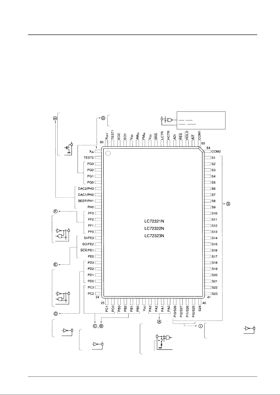
Pin Assignment
N-channel open-drain
output-only pins with 15-V
voltage handling capacity
PH2 and PH3 can be
switched to be used with the
D/A converter.*
2
PH1 can be switched to be
used as the beep tone
function pin.*
1
Input-only pins
The input voltage handling
capacity is 13 V
(maximum rating)
High voltage handling capacity
input ports (maximum ratings)
INT, RES, ADI
SNS, HOLD → 13 V
CMOS I/O
These pins can
be switched
between input
and output in
1-bit units.
CMOS I/O
These pins can be
switched between input
and output in 4-bit
units.
PE1, PE2, and PE3
can be switched to be
used by the SI/O
circuit.*
1
CMOS output-only
pins
Option
CMOS output-only pins (for key outputs or
similar functions)
These are unbalanced CMOS outputs and
pairs of these pins may be shorted together.
Input-only pins (for key inputs or
similar functions)
The presence or absence of built-in pulldown resistors can be selected.
Can be switch to function as
LCD segment outputs.
CMOS output-only pins
S1 through S28 can be
switched to function as
general-purpose CMOS
output ports.
(In the option
specifications)
Notes:*1. Only possible with the LC72321N
*2. Only possible with the LC72321N and LC72322N
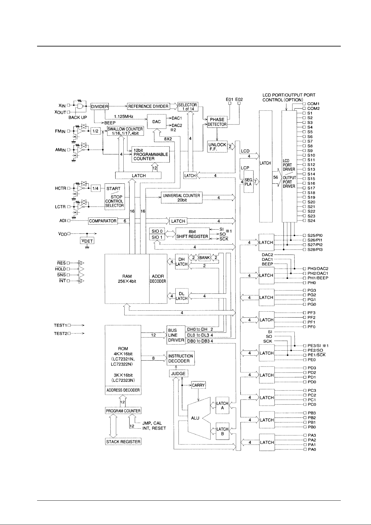
Block Diagram
No. 5945-3/13
LC72321N, 72322N, 72323N
Notes:*1. Only possible with the LC72321N
*2. Only possible with the LC72321N and LC72322N
Specifications
Absolute Maximum Ratings at Ta = 25°C, VSS= 0 V
Allowable Operating Ranges at Ta = –40 to +85°C, VDD= 3.5 to 5.5 V
No. 5945-4/13
LC72321N, 72322N, 72323N
Parameter Symbol Conditions Rating Unit
Maximum supply voltage V
DD
max –0.3 to +6.5 V
HOLD, INT, RES, ADI, SNS
–0.3 to +13 V
Input voltage
V
IN
1
Port G
V
IN
2 Inputs other than VIN1 –0.3 to VDD+ 0.3 V
Output voltage
V
OUT
1 Port H –0.3 to +15 V
V
OUT
2 Outputs other than V
OUT
1 –0.3 to VDD+ 0.3 V
I
OUT
1 All the port D and H pins 0 to 5 mA
Output current
I
OUT
2 All the port E and F pins 0 to 3 mA
I
OUT
3 All the port B and C pins 0 to 1 mA
I
OUT
4 S1 to S28 and port I 0 to 1 mA
Allowable power dissipation Pd max Ta = –40 to +85°C 300 mW
Operating temperature Topr –40 to +85 °C
Storage temperature Tstg –45 to +125 °C
Parameter Symbol Conditions
Ratings
Unit
min typ max
V
DD
1 CPU and PLL operating 4.5 5.5 V
Supply voltage V
DD
2 CPU operating 3.5 5.5 V
V
DD
3 Memory retention 1.3 5.5 V
V
IH
1 Port G 0.7 V
DD
8.0 V
V
IH
2 RES, INT, HOLD 0.8 V
DD
8.0 V
High-level input voltage
V
IH
3 SNS 2.5 8.0 V
V
IH
4 Port A 0.6 V
DD
V
DD
V
V
IH
5 Ports E and F 0.7 V
DD
V
DD
V
V
IH
6 LCTR (period measurement), VDD1, PE1, and PE3 0.8 V
DD
V
DD
V
V
IL
1 Port G 0 0.3 V
DD
V
V
IL
2 RES, INT, PE1, PE3 0 0.2 V
DD
V
V
IL
3 SNS 0 1.3 V
Low-level input voltage V
IL
4 Port A 0 0.2 V
DD
V
V
IL
5 PE0, PE2, and port F 0 0.3 V
DD
V
V
IL
6 LCTR (period measurement) and VDD1 0 0.2 V
DD
V
V
IL
7 HOLD 0 0.4 V
DD
V
f
IN
1 XIN 4.0 4.5 5.0 MHz
f
IN
2 FMIN, VIN2, VDD1 10 130 MHz
f
IN
3 FMIN, VIN3, VDD1 10 150 MHz
Input frequency
f
IN
4 AMIN (L), VIN4, VDD1 0.5 10 MHz
f
IN
5 AMIN (H), VIN5, VDD1 2.0 40 MHz
f
IN
6 HCTR, VIN6, VDD1 0.4 12 MHz
f
IN
7 LCTR (frequency), VIN7, and VDD1 100 500 kHz
f
IN
8 LCTR (period), VIH6, VIL6, and VDD1 1 20×10
3
Hz
V
IN
1 XIN 0.50 1.5 Vrms
V
IN
2 FMIN 0.10 1.5 Vrms
Input amplitude V
IN
3 FMIN 0.15 1.5 Vrms
V
IN
4, 5 AMIN 0.10 1.5 Vrms
V
IN
6, 7 LCTR, HCTR 0.10 1.5 Vrms
Input voltage range V
IN
8 ADI 0 V
DD
V
 Loading...