

SANYO LC651204L, LC651204F, LC651202N, LC651202L, LC651202F Datasheet
...
CMOS LSI
Ordering number : EN*5190
93096HA (OT) No. 5190-1/35
Preliminary
SANYO Electric Co.,Ltd. Semiconductor Bussiness Headquarters
TOKYO OFFICE Tokyo Bldg., 1-10, 1 Chome, Ueno, Taito-ku, TOKYO, 110 JAPAN
4-Bit Single-Chip Microcontrollers for Small-Scale
Control Applications
LC651204N/F/L, LC651202N/F/L
Overview
The LC651204N/F/L and LC651202N/F/L are small-scale
application microcontroller products in Sanyo's LC6500
series of 4-bit single-chip CMOS microcontrollers, and as
such they fully support the basic architecture and
instruction set of that series. These microcontrollers are
provided in a 30-pin package and include 2 kilobytes (KB)
and 4 KB of on-chip ROM. These products are
appropriate for use in a wide range of applications, from
applications that use a small number of controls and
circuits that were previously implemented in standard
logic to larger scale applications including audio
equipment such as decks and players, office equipment,
communications equipment, automotive equipment, and
home appliances. Except for the lack of an A/D converter,
these microcontrollers provide the same functionality as
the LC651104, 02N/F/L.
Features
• Fabricated in a CMOS process for low power (An
instruction-controlled standby function is provided.)
• ROM/RAM
LC651204N/F/L - ROM: 4K × 8 bits, RAM: 256 × 4 bits
LC651202N/F/L - ROM: 2K × 8 bits, RAM: 256 × 4 bits
• Instruction set: The 80-instruction set provided by all
members of the LC6500 series.
• Wide operating power-supply voltage range of 2.5 to 5.5
volts (L version)
• Instruction cycle time: 0.92 µs (F version)
• On-chip serial I/O circuit
• Highly flexible I/O ports
— Number of ports: 6 ports with a total of 22 pins
— All ports: Can be used for both input and output
I/O voltage: 15 V maximum (Only for C,
D, E, and F ports with opendrain output specifications)
Output current:20 mA maximum sink current
(Capable of directly driving
LEDs.)
— Options that allow specifications to be customized to
match those of the application system.
Specification of open-drain output or built-in pullup resistor: can be specified for all ports in bit
units.
Specification of the output level at reset: Can be
specified to be high or low for ports C and D in
port units.
• Interrupt functions
— Timer overflow vector interrupt (The interrupt state
can be tested by the CPU.)
— Vector interrupts initiated by the INT pin or
full/empty states of the serial I/O circuit. (The
interrupt state can be tested by the CPU.)
• Stack levels: 8 levels (shared with interrupts)
• Timers: 4-bit prescaler plus 8-bit programmable timers
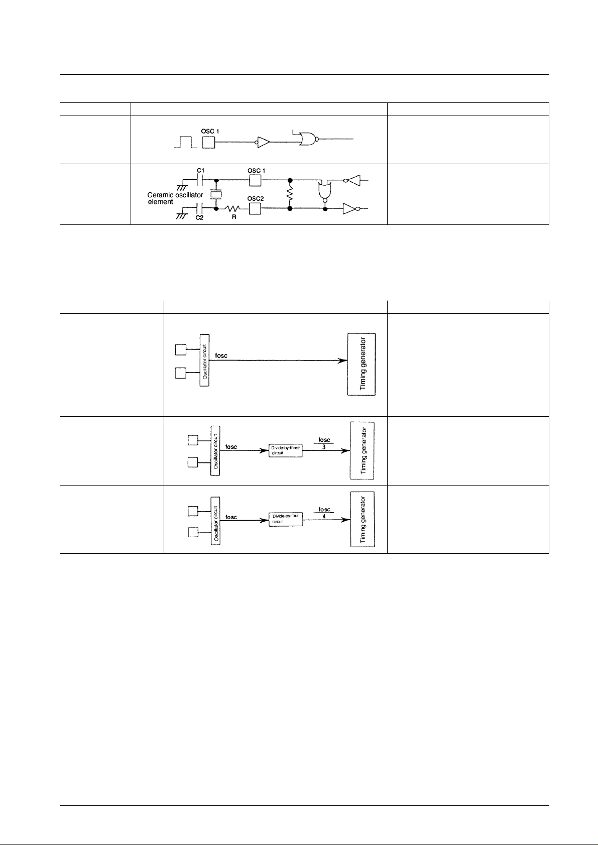
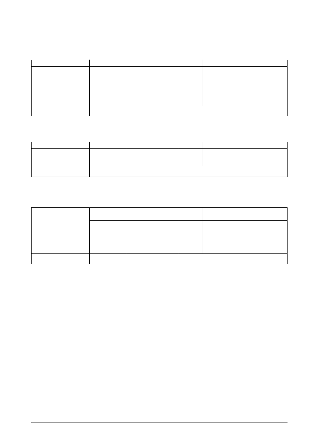
• Clock oscillator options to match application system
specifications.
— Oscillator circuit options: 2-pin ceramic oscillator (N,
F, and L versions)
— Divider circuit option: No divider, built-in divide-by-
three circuit, built-in divide-by-four circuit (N and L
versions)
• Supports continuous output of a square wave signal
(with a period 64 times the cycle time)
• Watchdog timer
— RC time constant scheme
— A watchdog timer function can be allocated to one of
the external pins as an option.
• EP version: LC65E1104, OTP version: LC65P1104
Function Overview
Note: Sanyo will announce details on oscillator elements and oscillator circuit constants as recommended application circuits are developed. Customers
should check with Sanyo for the latest information as the development process progresses.
No. 5190-2/35
LC651204N/F/L, LC651202N/F/L
Item LC651204N/1202N LC651204F/1202F LC651204L/1202L
ROM
4096 × 8 bits (1204N) 4096 × 8 bits (1204F) 4096 × 8 bits (1204L)
Memory 2048 × 8 bits (1202N) 2048 × 8 bits (1202F) 2048 × 8 bits (1202L)
RAM 256 × 4 bits (1204/1202N) 256 × 4 bits (1204/1202F) 256 × 4 bits (1204/1202L)
Instruction
Instruction set 80 80 80
Table reference Supported Supported Supported
Interrupts 1 external, 1 internal 1 external, 1 internal 1 external, 1 internal
Timers 4-bit prescaler + 8-bit timer 4-bit prescaler + 8-bit timer 4-bit prescaler + 8-bit timer
Built-in functions Stack levels 8 8 8
Standby function
Supports standby mode entered Supports standby mode entered Supports standby mode entered
by the HALT instruction by the HALT instruction by the HALT instruction
Number of ports 22 I/O pins 22 I/O pins 22 I/O pins
Serial ports 4-bit or 8-bit I/O 4-bit or 8-bit I/O 4-bit or 8-bit I/O
I/O voltage 15 V max. 15 V max. 15 V max.
I/O ports Output current 10 mA typ. 20 mA max. 10 mA typ. 20 mA max. 10 mA typ. 20 mA max.
I/O circuit types Open drain (n-channel) or built-in pull-up resistor output selectable on a per-bit basis.
Output levels at reset High or low can be selected in port units. (ports C and D only)
Square wave output Supported Supported Supported
Minimum cycle time 2.77 µs (V
DD
≥ 3 V) 0.92 µs (VDD≥ 3 V) 3.84 µs (VDD≥ 2.5 V)
Characteristics Power-supply voltage 3 to 5.5 V 3 to 5.5 V 2.5 to 5.5 V
Power-supply current 1.5 mA typ. 2 mA typ. 1.5 mA typ.
Oscillator
Oscillator Ceramic (800 kHz, 1 MHz, 4 MHz) Ceramic (4 MHz) Ceramic (800 kHz, 1 MHz, 4 MHz)
Divider circuit option 1/1, 1/3, 1/4 1/1 1/1, 1/3, 1/4
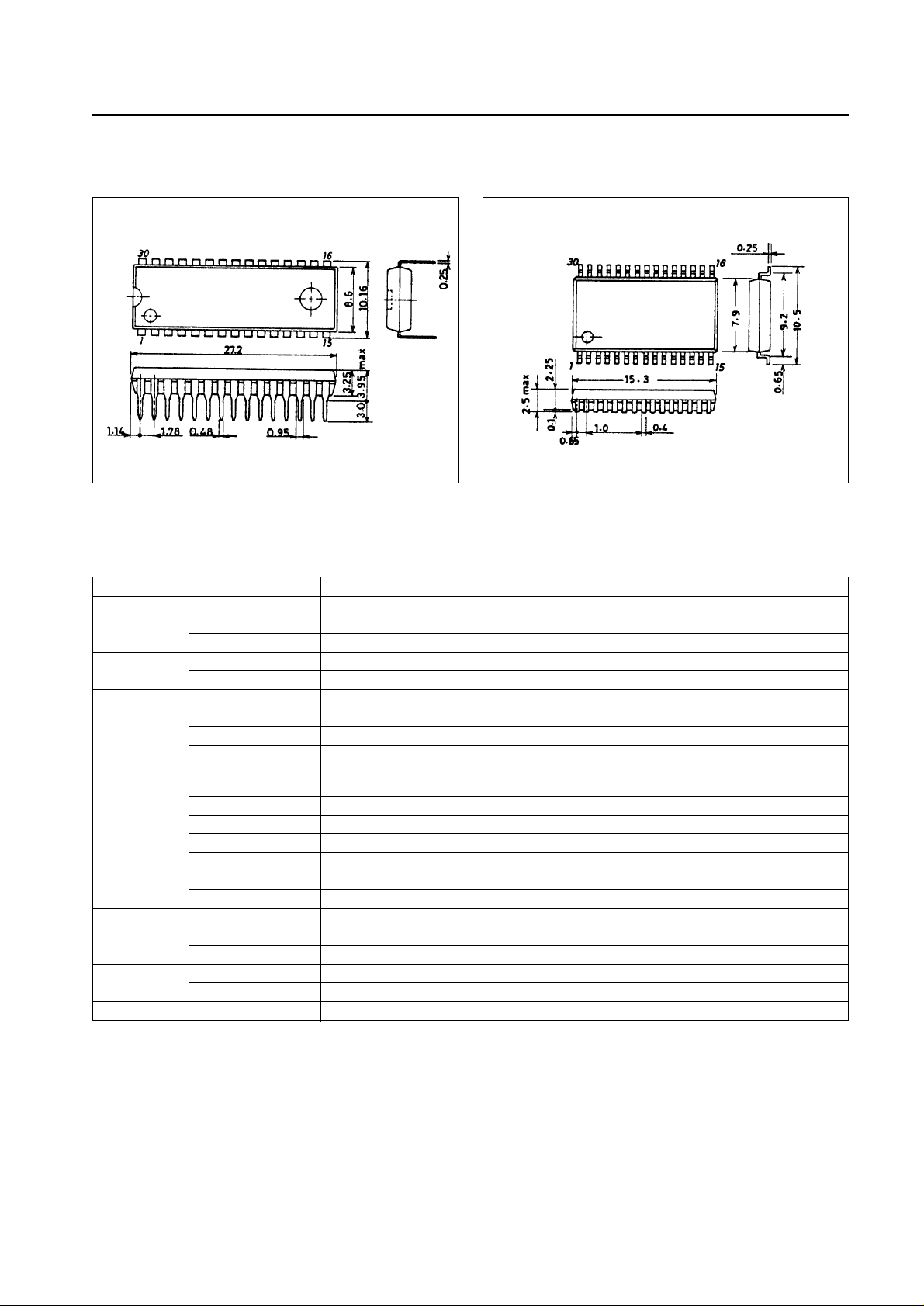
Other functions Package DIP30S-D MFP30S DIP30S-D MFP30S DIP30S-D MFP30S
SANYO: DIP30SD
[LC651204N/F/L, 651202N/F/L]
Note: The package drawings shown above are provided without error tolerances and are for reference purposes only. Contact Sanyo for official package
drawings.
SANYO: MFP30S
[LC651204N/F/L, 651202N/F/L]
Package Dimensions
unit : mm
3196-DIP30SD
unit : mm
3073A-MFP30S
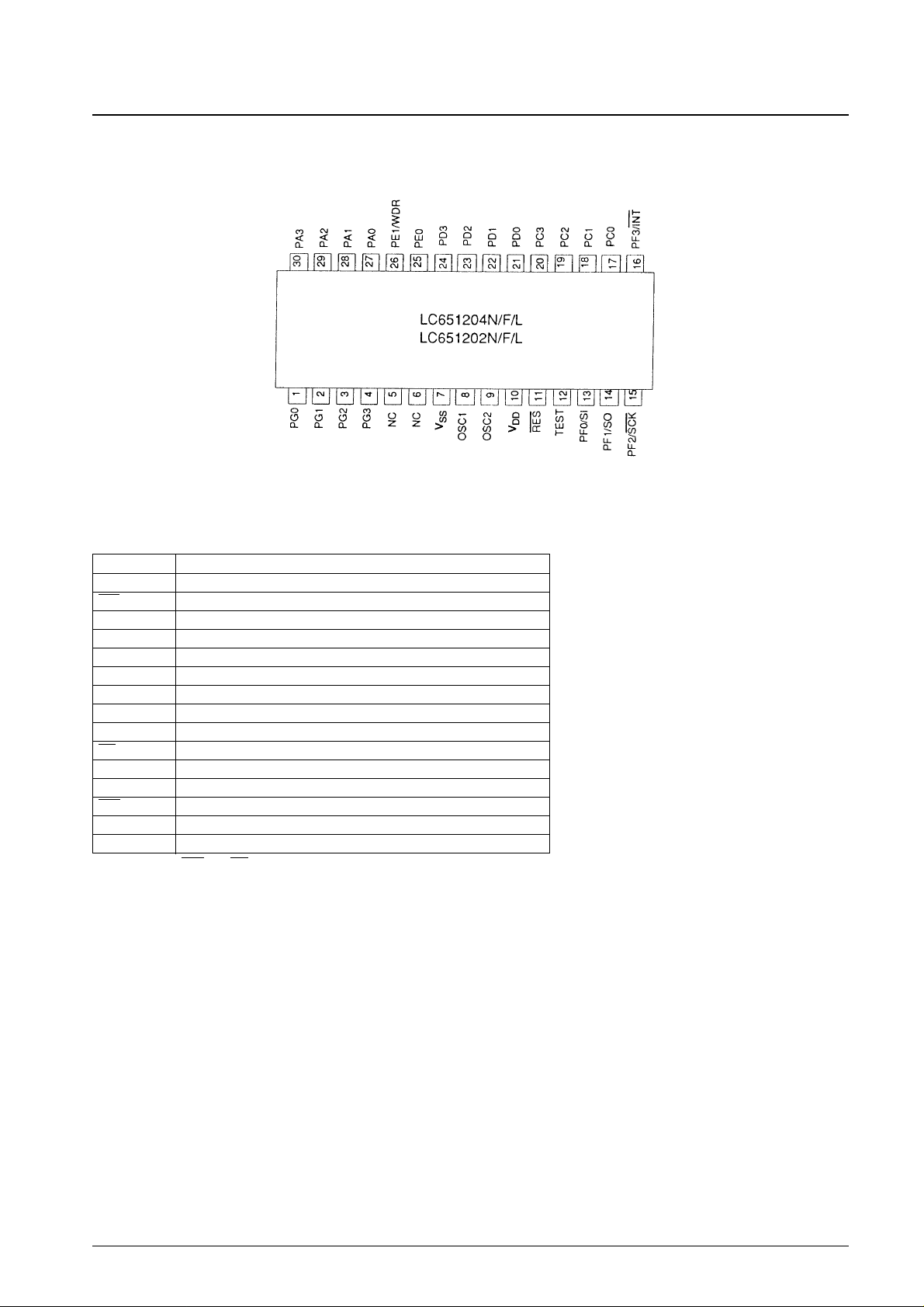
Pin Assignment
Common assignments for the DIP and MFP packages
Note: NC pins must be connected to VSS. Top view
Pin Functions
Note: The SI, SO, SCK, and INT pins are shared function pins that are also used as PF0 to PF3.
Pin Function
OSC1, OSC2 Connections for a ceramic oscillator element
RES Reset
PA0 to 3 I/O dual-function port A0 to A3
PC0 to 3 I/O dual-function port C0 to C3
PD0 to 3 I/O dual-function port D0 to D3
PE0 to 1 I/O dual-function port E0 to E1
PF0 to 3 I/O dual-function port F0 to F3
PG0 to 3 I/O dual-function port G0 to G3
TEST Test
INT Interrupt request
SI Serial input
SO Serial output
SCK Serial clock input and output
NC No connection
WDR Watchdog reset
No. 5190-3/35
LC651204N/F/L, LC651202N/F/L
System Block Diagram
RAM: Data memory ROM: Program memory
F: Flag PC: Program counter
WR: Working register INT: Interrupt control
AC: Accumulator IR: Instruction register
ALU: Arithmetic and logic unit I.DEC: Instruction decoder
DP: Data pointer CF, CSF: Carry flag, carry save flag
E: E register ZF, ZSF: Zero flag, zero save flag
CTL: Control register EXTF: External interrupt request flag
OSC: Oscillator circuit TMF: Internal interrupt request flag
TM: Timer
STS: Status register
No. 5190-4/35
LC651204N/F/L, LC651202N/F/L
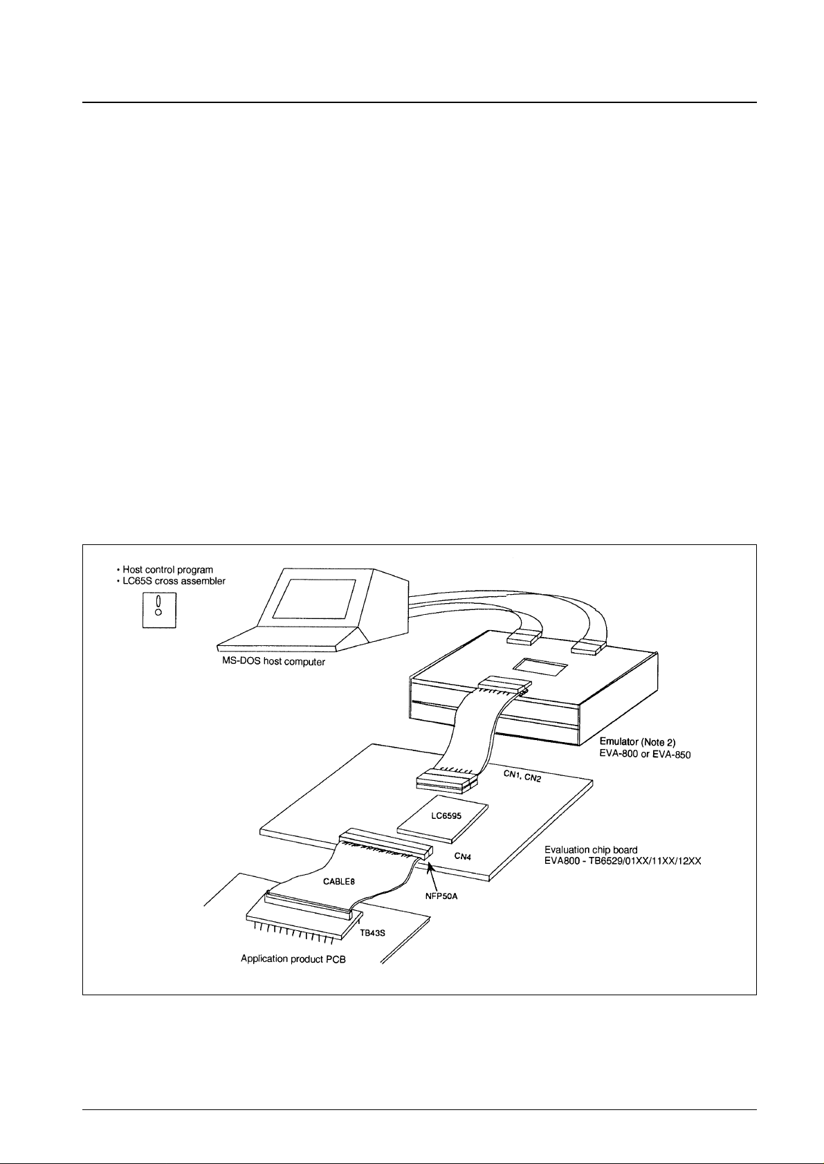
Development Support
Sanyo provides the following items to support application development using the LC651204 and LC651202.
1. User’s manual
The “LC651104/1102 User’s Manual” is used with these microcontrollers.
2. Development tool manual
See the “EVA800 - LC651104/1102 Development Tool Manual” for details on use of the EVA-800 system.
3. Development tool
• Program development (using the EVA-800 system)
— MS-DOS host computer system *1
— Cross assembler ... MS-DOS-based cross assembler: LC65S.EXE
— Evaluation chip: LC6595
— Emulator: The EVA-800 main unit plus the evaluation chip
• Program development (using the EVA-86000 system): Use the EVA86K-ECB651100.
• Program evaluation
The <LC65E1104> on-chip EPROM microcontroller
Development Support System
EVA-800 System
Note: 1. MS-DOS is a registered trademark of Microsoft Corporation
2. Here, “EVA-800” is a generic term for several emulators. Suffixes (A, B, etc.) will be attached to the name as new versions are developed. Note that
the EVA-800 emulator (i.e., the model with no suffix) is an old version and cannot be used.
No. 5190-5/35
LC651204N/F/L, LC651202N/F/L

Pin Functions
No. 5190-6/35
Pin
V
DD
V
SS
OSC1
OSC2
PA0 to
PA3
PC0 to
PC3
PD0 to
PD3
Pin no.
1
1
1
1
4
4
4
I/O
—
—
Input
Output
I/O
I/O
I/O
Function
Power supply
• System clock oscillator
Connect an external ceramic oscillator
element to these pins
• Leave OSC2 open if an external clock
is supplied.
• I/O port A0 to A3
Input in 4-bit units using the IP
instruction
Output in 4-bit units using the OP
instruction
Port bits can be tested in bit units using
the BP and BNP instructions.
Port bits can be set or cleared in bit
units using the SPB and RPB
instructions.
• PA3 is used for standby control.
• Applications must be designed so that
no chattering (e.g. switch bounce)
occurs on the PA3 pin during a HALT
instruction execution cycle.
• I/O port C0 to C3
The PC0 to PC3 pin functions are
identical to those of the PA0 to 3 pins.*
• High or low can be specified as the
output at reset as an option.
Note: These pins do not have a
standby control function.
• I/O port D0 to D3
The PD0 to PD3 pin functions and
options are identical to those of the
PC0 to PC3 pins.
Options
—
(1) External clock
(2) Two-pin ceramic oscillator
(3) Divider circuit option
1. No divider circuit
2. Divide-by-three circuit
3. Divide-by-four circuit
(1) Output open drain
(2) Built-in pull-up resistor
• Options (1) and (2) can be
specified in bit units.
(1) Output open drain
(2) Built-in pull-up resistor
(3) High-level output at reset
(4) Low-level output at reset
• Options (1) and (2) can be
specified in bit units.
• Option (3) and (4) are
specified in 4-bit units.
The same as PC0 to PC3.
State at reset
—
—
High-level output
(i.e., the output
n-channel
transistor will be
off.)
• High-level
output
• Low-level
output
(Depending on
the option
specified.)
The same as
PC0 to PC3.
Handling when unused
—
—
Open drain output select
the options, connect to
V
SS
.
The same as PA0 to
PA3.
The same as PA0 to
PA3.
LC651204N/F/L, LC651202N/F/L
Continued on next page.

No. 5190-7/35
LC651204N/F/L, LC651202N/F/L
Pin
PE0 to
PE1
/WDR
PF0/SI
PF1/SO
PF2/SCK
PF3/INT
PG0 to
PG3
NC
RES
TEST
Pin no.
2
4
4
2
1
1
I/O
I/O
I/O
I/O
Input
Input
Function
• I/O port E0 to E1
Input in 4-bit units using the IP
instruction
Output in 4-bit units using the OP
instruction
Port bits can be set or cleared in bit
units using the SPB and RPB
instructions.
Port bits can be tested in bit units using
the BP and BNP instructions.
• The PE0 pin also has a continuous
pulse (64·Tcyc) output function.
• The PE1 pin can be set to function as
the WDR watchdog timer reset pin as
an option.
• I/O port F0 to F3
This port has the same functions and
options as PE0 to PE1. *
• The pins PF0 to PF3 are also used as
the serial interface and the INT pin.
The function used can be selected
under program control.
SI ······Serial input port
SO·····Serial output port
SCK ··Serial clock input or output
INT····Interrupt request input
Serial I/O can be switched between 4bit and 8-bit operation under program
control.
Note: This port does not provide a
continuous pulse output function.
• I/O port G0 to G3
This port has the same functions and
options as PE0 to PE1. *
Note: This port does not provide a
continuous pulse output function.
• NC pin. This pin must be connected to
V
SS
in the EP and OTP versions.
• System reset input
• Connect an external capacitor for the
power up reset.
• A low level must be applied for at least
four clock cycles for the reset startup
sequence to operate correctly.
• LSI test pin
Must be connected to V
SS
.
Options
(1) Output open drain
(2) Built-in pull-up resistor
• Options (1) and (2) can be
specified in bit units.
(3) Normal port PE1
(4) Watchdog timer reset WDR
(5) (3) or (4) can be specified.
The same as PA0 to PA3.
The same as PA0 to PA3.
—
—
—
State at reset
High-level output
(i.e., the output
n-channel
transistor will be
off.)
The same as
PA0 to PA3.
The serial port
function is
disabled.
The interrupt
source is INT.
The same as
PA0 to PA3.
—
—
—
Handling when unused
The same as PA0 to
PA3.
The same as PA0 to
PA3.
The same as PA0 to
PA3.
Connect to V
SS
.
—
Must be connected to
V
SS
.
Continued from preceding page.
Oscillator Circuit Options
Divider Options
Caution: The oscillator and divider options are summarized in the following tables. The information presented in those tables is crucial when using these
products.
No. 5190-8/35
LC651204N/F/L, LC651202N/F/L
Option Circuit Conditions and notes
The OSC2 pin must be left open.
External clock
Ceramic oscillator
Option Circuit Conditions and notes
• Supports both oscillator options.
• The oscillator frequency or the external clock
frequency must not exceed 1444 kHz
(LC651204N and LC651202N)
No divider (1/1) • The oscillator frequency or the external clock
frequency must not exceed 4330 kHz
(LC651204F and LC651202F)
• The oscillator frequency or the external clock
frequency must not exceed 1040 kHz
(LC651204L and LC651202L)
• Supports both oscillator options.
• The oscillator frequency or the external clock
frequency must not exceed 4330 kHz
Built-in divide-by-three circuit
• Supports both oscillator options.
• The oscillator frequency or the external clock
frequency must not exceed 4330 kHz
Built-in divide-by-four circuit
Divider Options for the LC651204N/1202N, LC651204F/1202F, and LC651204L/1202L
LC651204N, LC651202N
No. 5190-9/35
LC651204N/F/L, LC651202N/F/L
Circuit type Frequency Divider option (cycle time) VDDrange Notes
800 kHz 1/1 (5 µs) 3 to 5.5 V
Ceramic oscillator
1 MHz 1/1 (4µs) 3 to 5.5 V
4 MHz
1/3 (3µs) 3 to 5.5 V This frequency cannot be used with the 1/1
1/4 (4µs) 3 to 5.5 V divider (i.e., no divider circuit) option.
External clock generated by a
670 k to 1444 kHz 1/1 (6 to 2.77 µs) 3 to 5.5 V
two-terminal RC oscillator circuit
2000 k to 4330 kHz 1/3 (6 to 2.77 µs) 3 to 5.5 V
2600 k to 4330 kHz 1/4 (6 to 3.70 µs) 3 to 5.5 V
Use of an external clock with the Driving the circuit with an external clock is not possible. To use external clock drive, specify the two-terminal RC
ceramic oscillator option selected oscillator option.
LC651204L LC651202L
Circuit type Frequency Divider option (cycle time) VDDrange Notes
800 kHz 1/1 (5 µs) 2.5 to 5.5 V
Ceramic oscillator
1 MHz 1/1 (4µs) 2.5 to 5.5 V
4 MHz 1/4 (4µs) 2.5 to 5.5 V
This frequency cannot be used with the 1/1, 1/3
divider (i.e., no divider circuit) option.
External clock generated by a
670 k to 1040 kHz 1/1 (6 to 3.84 µs) 2.5 to 5.5 V
two-terminal RC oscillator circuit
2000 k to 3120 kHz 1/3 (6 to 3.84 µs) 2.5 to 5.5 V
2600 k to 4160 kHz 1/4 (6 to 3.84 µs) 2.5 to 5.5 V
Use of an external clock with the Driving the circuit with an external clock is not possible. To use external clock drive, specify the two-terminal RC
ceramic oscillator option selected oscillator option.
LC651204F, LC651202F
Circuit type Frequency Divider option (cycle time) VDDrange Notes
Ceramic oscillator 4 MHz 1/1 (1 µs) 3 to 5.5 V
External clock generated by a
670 k to 4330 kHz 1/1 (6 to 0.92 µs) 3 to 5.5 V
two-terminal RC oscillator circuit
Use of an external clock with the Driving the circuit with an external clock is not possible. To use external clock drive, specify the two-terminal RC
ceramic oscillator circuit oscillator option.

Port C and D Output State at Reset Options
The output levels at reset of the I/O ports C and D can be selected from the following two options, which are specified in
4-bit units.
Port Output Circuit Type Option
The output circuit types of the I/O ports can be selected from the following two options in bit units.
Watchdog Timer Reset Option
Whether the PE1/WDR pin functions as the normal port PE1 or as the WDR watchdog timer reset pin can be selected as
an option.
No. 5190-10/35
LC651204N/F/L, LC651202N/F/L
Option Conditions and notes
High-level output at reset Ports C and D in 4-bit units
Low-level output at reset Ports C and D in 4-bit units
Option Circuit Conditions and notes
Ports A, C, D, E, F, and G
Open drain output
Pull-up resistor output
LC651204N, 651202N
Absolute Maximum Ratings at Ta = 25°C, VSS= 0 V
No. 5190-11/35
LC651204N/F/L, LC651202N/F/L
Parameter Symbol Conditions Applicable pins/notes Ratings Unit
Maximum supply voltage V
DD
max V
DD
–0.3 to +7.0 V
Voltages up to any
Output voltage V
O
OSC2 generated voltage are V
allowed.
Input voltage
VI(1) OSC1 *1 –0.3 to VDD+0.3 V
V
I
(2) TEST, RES –0.3 to VDD+0.3 V
V
IO
(1) PC0 to 3, PD0 to 3, PE0, 1, PF0 to 3 OD specification ports –0.3 to + 15 V
I/O voltage V
IO
(2) PC0 to 3, PD0 to 3, PE0, 1, PF0 to 3 PU specification ports –0.3 to VDD+0.3 V
V
IO
(3) PA0 to 3, PG0 to 3 –0.3 to VDD+0.3 V
Peak output current I
OP
I/O ports –2 to +20 mA
I
OA
Average value per pin over a 100-ms period I/O ports –2 to +20 mA
Σ IOA(1)
Total current for pins PC0 to 3, PD0 to 3, and
PC0 to PC3
PE0 to 1*2
PD0 to PD3 –15 to +100 mA
Average output current PE0 to PE1
Σ I
OA
(2)
Total current for pins PF0 to 3, PG0 to 3, and
PF0 to PF3
PA0 to 3*2
PG0 to PG3 –15 to +100 mA
PA0 to PA3
Allowable power Pd max (1) Ta = –40 to +85°C (DIP package) 250 mW
dissipation Pd max (2) Ta = –40 to +85°C (MFP package) 150 mW
Operating temperature Topr –40 to +85 °C
Storage temperature Tstg –55 to +125 °C
Allowable Operating Ranges at Ta = –40 to 85°C, VSS= 0 V, VDD= 3.0 to 5.5 V (unless otherwise specified)
Parameter Symbol Conditions Applicable pins/notes
Ratings
min typ max Unit
Operating power-supply
V
DD
V
DD
3.0 5.5 V
voltage
Standby power-supply
V
ST
RAM and register values retained *3 V
DD
1.8 5.5 V
voltage
VIH(1) Output n-channel transistors off
OD specification ports C, D, E,
0.7 V
DD
13.5 V
and F
VIH(2) Output n-channel transistors off
PU specification ports C, D, E,
0.7 V
DD
V
DD
V
and F
V
IH
(3) Output n-channel transistors off Port A, G 0.7 V
DD
V
DD
V
Input high-level voltage
V
IH
(4) Output n-channel transistors off
The INT, SCK, and SI pins with
0.8 V
DD
13.5 V
OD specifications
VIH(5) Output n-channel transistors off
The INT, SCK, and SI pins with
0.8 V
DD
V
DD
V
PU specifications
V
IH
(6) VDD= 1.8 to 5.5 V RES 0.8 V
DD
V
DD
V
V
IH
(7) External clock specifications OSC1 0.8 V
DD
V
DD
V
Continued on next page.
 Loading...