

Page 1

21-S3-C9228/P9228-112002
USER'S MANUAL
S3C9228/P9228
8-Bit CMOS
Microcontroller
Revision 1
Page 2

S3C9228/P9228
8-BIT CMOS
MICROCONTROLLERS
USER'S MANUAL
Revision 1
Page 3

Important Notice
The information in this publication has been
carefully checked and is believed to be entirely
accurate at the time of publication. Samsung
assumes no responsibility, however, for possible
errors or omissions, or for any consequences
resulting from the use of the information contained
herein.
Samsung reserves the right to make changes in its
products or product specifications with the intent to
improve function or design at any time and without
notice and is not required to update this
documentation to reflect such changes.
This publication does not convey to a purchaser of
semiconductor devices described herein any license
under the patent rights of Samsung or others.
Samsung makes no warranty, representation, or
guarantee regarding the suitability of its products for
any particular purpose, nor does Samsung assume
any liability arising out of the application or use of
any product or circuit and specifically disclaims any
and all liability, including without limitation any
consequential or incidental damages.
"Typical" parameters can and do vary in different
applications. All operating parameters, including
"Typicals" must be validated for each customer
application by the customer's technical experts.
Samsung products are not designed, intended, or
authorized for use as components in systems
intended for surgical implant into the body, for other
applications intended to support or sustain life, or for
any other application in which the failure of the
Samsung product could create a situation where
personal injury or death may occur.
Should the Buyer purchase or use a Samsung
product for any such unintended or unauthorized
application, the Buyer shall indemnify and hold
Samsung and its officers, employees, subsidiaries,
affiliates, and distributors harmless against all
claims, costs, damages, expenses, and reasonable
attorney fees arising out of, either directly or
indirectly, any claim of personal injury or death that
may be associated with such unintended or
unauthorized use, even if such claim alleges that
Samsung was negligent regarding the design or
manufacture of said product.
S3C9228/P9228 8-Bit CMOS Microcontrollers
User's Manual, Revision 1
Publication Number: 21-S3-C9228/P9228-112002
© 2002 Samsung Electronics
All rights reserved. No part of this publication may be reproduced, stored in a retrieval system, or transmitted in
any form or by any means, electric or mechanical, by photocopying, recording, or otherwise, without the prior
written consent of Samsung Electronics.
Samsung Electronics' microcontroller business has been awarded full ISO-14001
certification (BVQI Certificate No 9330) All semiconductor products are designed
and manufactured in accordance with the highest quality standards and
objectives.
Samsung Electronics Co., Ltd.
San #24 Nongseo-Ri, Kiheung-Eup
Yongin-City, Kyunggi-Do, Korea
C.P.O. Box #37, Suwon 449-900
TEL: (82)-(331)-209-1907
FAX: (82)-(331)-209-1889
Home-Page URL: Http://www.samsungsemi.com
Printed in the Republic of Korea
Page 4

Preface
The S3C9228/P9228 Microcontrollers User's Manual is designed for application designers and programmers who
are using the S3C9228/P9228 microcontrollers for application development. It is organized in two main parts:
Part I Programming Model Part II Hardware Descriptions
Part I contains software-related information to familiarize you with the microcontroller's architecture,
programming model, instruction set, and interrupt structure. It has six chapters:
Chapter 1 Product Overview
Chapter 2 Address Spaces
Chapter 3 Addressing Modes
Chapter 1, "Product Overview," is a high-level introduction to the 100% with general product descriptions, as well
as detailed information about individual pin characteristics and pin circuit types.
Chapter 2, "Address Spaces," explains the 100% program and data memory, internal register file, and mapped
control register, and explains how to address them. Chapter 2 also describes working register addressing, as well
as system stack and user-defined stack operations.
Chapter 3, "Addressing Modes," contains detailed descriptions of the addressing modes that are supported by the
CPU.
Chapter 4, "Control Registers," contains overview tables for all mapped system and peripheral control register
values, as well as detailed one-page descriptions in standard format. You can use these easy-to-read,
alphabetically organized, register descriptions as a quick-reference source when writing programs.
Chapter 5, "Interrupt Structure," describes the 100% interrupt structure in detail and further prepares you for
additional information presented in the individual hardware module descriptions in Part II.
Chapter 6, "SAM88RCRI Instruction Set," describes the features and conventions of the instruction set used for
all S3C9-series microcontrollers. Several summary tables are presented for orientation and reference. Detailed
descriptions of each instruction are presented in a standard format. Each instruction description includes one or
more practical examples of how to use the instruction when writing an application program.
A basic familiarity with the information in Part I will help you to understand the hardware module descriptions in
Part II. If you are not yet familiar with the SAM8 product family and are reading this manual for the first time, we
recommend that you first read chapters 1–3 carefully. Then, briefly look over the detailed information in chapters
4, 5, and 6. Later, you can reference the information in Part I as necessary.
Part II "hardware Descriptions," has detailed information about specific hardware components of the
S3C9228/P9228 microcontrollers. Also included in Part II are electrical, mechanical, OTP, and development
tools data. It has 13 chapters:
Chapter 4 Control Registers
Chapter 5 Interrupt Structure
Chapter 6 SAM88RCRI Instruction Set
Chapter 7 Clock Circuits
Chapter 8 RESET and Power-Down
Chapter 9 I/O Ports
Chapter 10 Basic Timer
Chapter 11 Timer 1
Chapter 12 Watch Timer
Chapter 13 LCD Controller/Driver
Two order forms are included at the back of this manual to facilitate customer order for S3C9228/P9228
microcontrollers: the Mask ROM Order Form, and the Mask Option Selection Form. You can photocopy these
forms, fill them out, and then forward them to your local Samsung Sales Representative.
S3C9228/P9228 MICROCONTROLLERS iii
Chapter 14 10-bit ADC
Chapter 15 Serial I/O Interface
Chapter 16 Electrical Data
Chapter 17 Mechanical Data
Chapter 18 S3P9228 OTP
Chapter 19 Development Tools
Page 5

Page 6

Table of Contents
Part I — Programming Model
Chapter 1 Product Overview
SAM88RCRI Product Family ...................................................................................................................1-1
S3C9228/P9228 Microcontroller ..............................................................................................................1-1
OTP.........................................................................................................................................................1-1
Features..................................................................................................................................................1-2
Block Diagram.........................................................................................................................................1-3
Pin Assignments......................................................................................................................................1-4
Pin Descriptions.......................................................................................................................................1-6
Pin Circuit Diagrams................................................................................................................................1-8
Chapter 2 Address Spaces
Overview.................................................................................................................................................2-1
Program Memory (ROM) .........................................................................................................................2-2
Register Architecture ...............................................................................................................................2-3
Common Working Register Area (C0H–CFH)..........................................................................................2-4
System Stack ..........................................................................................................................................2-5
Chapter 3 Addressing Modes
Overview.................................................................................................................................................3-1
Register Addressing Mode (R).........................................................................................................3-2
Indirect Register Addressing Mode (IR) ...........................................................................................3-3
Indexed Addressing Mode (X)..........................................................................................................3-7
Direct Address Mode (DA)...............................................................................................................3-10
Relative Address Mode (RA) ...........................................................................................................3-12
Immediate Mode (IM)......................................................................................................................3-12
S3C9228/P9228 MICROCONTROLLERS v
Page 7

Table of Contents (Continued)
Chapter 4 Control Registers
Overview.................................................................................................................................................4-1
Chapter 5 Interrupt Structure
Overview.................................................................................................................................................5-1
Interrupt Processing Control Points..................................................................................................5-1
Enable/Disable Interrupt Instructions (EI, DI) ................................................................................... 5-1
Interrupt Pending Function Types....................................................................................................5-2
Interrupt Priority...............................................................................................................................5-2
Interrupt Source Service Sequence .................................................................................................5-3
Interrupt Service Routines...............................................................................................................5-3
Generating Interrupt Vector addresses.............................................................................................5-3
S3C9228/P9228 Interrupt Structure.................................................................................................5-4
Chapter 6 SAM88RCRI Instruction Set
Overview.................................................................................................................................................6-1
Register Addressing.........................................................................................................................6-1
Addressing Modes...........................................................................................................................6-1
Flags Register (FLAGS) ..................................................................................................................6-4
Flag Descriptions .............................................................................................................................6-4
Instruction Set Notation ................................................................................................................... 6-5
Condition Codes..............................................................................................................................6-9
Instruction Descriptions....................................................................................................................6-10
vi S3C9228/P9228 MICROCONTROLLERS
Page 8

Table of Contents (Continued)
Part II — Hardware Descriptions
Chapter 7 Clock Circuit
Overview.................................................................................................................................................7-1
System Clock Circuit.......................................................................................................................7-1
CPU Clock Notation ........................................................................................................................7-1
Main Oscillator Circuits....................................................................................................................7-2
Sub Oscillator Circuits.....................................................................................................................7-2
Clock Status During Power-Down Modes.........................................................................................7-3
System Clock Control Register (CLKCON)......................................................................................7-4
Oscillator Control Register (OSCCON)............................................................................................7-5
Switching The CPU Clock................................................................................................................7-6
Stop Control Register (STPCON) ....................................................................................................7-7
Chapter 8 RESETRESET and Power-Down
System Reset..........................................................................................................................................8-1
Overview.........................................................................................................................................8-1
Power-Down Modes.................................................................................................................................8-2
Stop Mode.......................................................................................................................................8-2
Idle Mode........................................................................................................................................8-3
Hardware Reset Values...................................................................................................................8-4
Chapter 9 I/O Ports
Overview.................................................................................................................................................9-1
Port Data Registers.........................................................................................................................9-2
Port 0..............................................................................................................................................9-3
Port 1..............................................................................................................................................9-6
Port 2..............................................................................................................................................9-9
Port 3..............................................................................................................................................9-11
Port 4..............................................................................................................................................9-14
Port 5..............................................................................................................................................9-15
Port 6..............................................................................................................................................9-16
Chapter 10 Basic Timer
Overview.................................................................................................................................................10-1
Basic Timer Control Register (BTCON)...........................................................................................10-2
Basic Timer Function Description....................................................................................................10-3
S3C9228/P9228 MICROCONTROLLERS vii
Page 9

Table of Contents (Continued)
Chapter 11 Timer 1
One 16-Bit Timer Mode (Timer 1)............................................................................................................11-1
Overview.........................................................................................................................................11-1
Function Description........................................................................................................................11-1
Two 8-Bit Timers Mode (Timer A and B)..................................................................................................11-4
Overview.........................................................................................................................................11-4
Function Description........................................................................................................................11-7
Chapter 12 Watch Timer
Overview.................................................................................................................................................12-1
Watch Timer Control Register (WTCON).........................................................................................12-2
Watch Timer Circuit Diagram...................................................................................................................12-3
Chapter 13 LCD Controller/Driver
Overview.................................................................................................................................................13-1
LCD Circuit Diagram........................................................................................................................13-2
LCD RAM Address Area..................................................................................................................13-3
LCD Mode Control Register (LMOD)................................................................................................13-4
LCD Port Control Register...............................................................................................................13-5
LCD Voltage Dividing Resistors....................................................................................................... 13-6
Common (COM) Signals..................................................................................................................13-6
Segment (SEG) Signals...................................................................................................................13-6
Chapter 14 10-Bit A/D Converter
Overview.................................................................................................................................................14-1
Function Description................................................................................................................................14-1
Conversion Timing .......................................................................................................................... 14-2
A/D Converter Control Register (ADCON) ....................................................................................... 14-2
Internal Reference Voltage Levels................................................................................................... 14-3
Block Diagram.........................................................................................................................................14-3
Chapter 15 Serial I/O Interface
Overview.................................................................................................................................................15-1
Programming Procedure..................................................................................................................15-1
SIO Control Registers (SIOCON).....................................................................................................15-2
SIO Pre-Scaler Register (SIOPS)....................................................................................................15-3
SIO Block Diagram..................................................................................................................................15-3
Serial I/O Timing Diagram (SIO)......................................................................................................15-4
viii S3C9228/P9228 MICROCONTROLLERS
Page 10

Table of Contents (Concluded)
Chapter 16 Electrical Data
Overview.................................................................................................................................................16-1
Chapter 17 Mechanical Data
Overview.................................................................................................................................................17-1
Chapter 18 S3P9228 OTP
Overview.................................................................................................................................................18-1
Operating Mode Characteristics.......................................................................................................18-3
Chapter 19 Development Tools
Overview.................................................................................................................................................19-1
SHINE.............................................................................................................................................19-1
SAMA Assembler............................................................................................................................19-1
SASM86..........................................................................................................................................19-1
HEX2ROM ......................................................................................................................................19-1
Target Boards..................................................................................................................................19-1
TB9228 Target Board......................................................................................................................19-3
Idle LED..........................................................................................................................................19-5
Stop LED.........................................................................................................................................19-5
S3C9228/P9228 MICROCONTROLLERS ix
Page 11

Page 12

List of Figures
Figure Title Page
Number Number
1-1 Block Diagram ....................................................................................................................1-3
1-2 S3C9228 44-QFP Pin Assignments....................................................................................1-4
1-3 S3C9228 42-SDIP Pin Assignments...................................................................................1-5
1-4 Pin Circuit Type B ..............................................................................................................1-8
1-5 Pin Circuit Type C ..............................................................................................................1-8
1-7 Pin Circuit Type E-4 ...........................................................................................................1-9
1-8 Pin Circuit Type F-16A .......................................................................................................1-9
1-9 Pin Circuit Type H-23 .........................................................................................................1-10
1-10 Pin Circuit Type H-32 .........................................................................................................1-11
1-11 Pin Circuit Type H-32A.......................................................................................................1-11
1-12 Pin Circuit Type H-32B.......................................................................................................1-12
2-1 S3C9228/P9228 Program Memory Address Space.............................................................2-2
2-2 Internal Register File Organization .....................................................................................2-3
2-3 16-Bit Register Pairs...........................................................................................................2-4
2-4 Stack Operations................................................................................................................2-5
3-1 Register Addressing ...........................................................................................................3-2
3-2 Working Register Addressing .............................................................................................3-2
3-3 Indirect Register Addressing to Register File ......................................................................3-3
3-4 Indirect Register Addressing to Program Memory...............................................................3-4
3-5 Indirect Working Register Addressing to Register File ........................................................3-5
3-6 Indirect Working Register Addressing to Program or Data Memory.....................................3-6
3-7 Indexed Addressing to Register File ...................................................................................3-7
3-8 Indexed Addressing to Program or Data Memory with Short Offset.....................................3-8
3-9 Indexed Addressing to Program or Data Memory with Long Offset.....................................3-9
3-10 Direct Addressing for Load Instructions...............................................................................3-10
3-11 Direct Addressing for Call and Jump Instructions................................................................3-11
3-12 Relative Addressing............................................................................................................3-12
3-13 Immediate Addressing........................................................................................................3-12
4-1 Register Description Format...............................................................................................4-4
S3C9228/P9228 MICROCONTROLLERS xi
Page 13

List of Figures (Continued)
Figure Title Page
Number Number
5-1 S3C9-Series Interrupt Type ................................................................................................ 5-1
5-2 Interrupt Function Diagram.................................................................................................5-2
5-3 S3C9228/P9228 Interrupt Structure....................................................................................5-5
6-1 System Flags Register (FLAGS).........................................................................................6-4
7-1 Crystal/Ceramic Oscillator..................................................................................................7-2
7-2 External Oscillator..............................................................................................................7-2
7-3 RC Oscillator......................................................................................................................7-2
7-4 Crystal/Ceramic Oscillator..................................................................................................7-2
7-5 External Oscillator..............................................................................................................7-2
7-6 System Clock Circuit Diagram............................................................................................7-3
7-7 System Clock Control Register (CLKCON) ......................................................................... 7-4
7-8 Oscillator Control Register (OSCCON) ...............................................................................7-5
7-9 STOP Control Register (STPCON).....................................................................................7-7
9-1 S3C9228 I/O Port Data Register Format .............................................................................9-2
9-2 Port 0 Control Register (P0CON)........................................................................................9-4
9-3 Port 0 Interrupt Control Register (P0INT)............................................................................9-4
9-4 Port 0 Interrupt Pending Bits (INTPND1.3-.0)......................................................................9-5
9-5 Port 0 Interrupt Edge Selection Register (P0EDGE)............................................................9-5
9-6 Port 0 Pull-up Control Register (P0PUR) ............................................................................9-5
9-7 Port 1 Control Register (P1CON)........................................................................................9-6
9-8 Port 1 Interrupt Control Register (P1INT)............................................................................9-7
9-9 Port 1 Interrupt Pending Bits (INTPND1.7-.4)......................................................................9-7
9-10 Port 1 Interrupt Edge Selection Register (P1EDGE)............................................................9-8
9-11 Port 1 Pull-up Control Register (P1PUR) ............................................................................9-8
9-12 Port 2 Control Register (P2CON)........................................................................................9-9
9-13 Port 2 Pull-up Control Register (P2PUR) ............................................................................9-10
9-14 Port 3 Control Register (P3CON)........................................................................................9-11
9-15 Port 3 Interrupt Control Register (P3INT)............................................................................9-12
9-16 Port 3 Interrupt Pending Bits (INTPND2.5-.4)......................................................................9-12
9-17 Port 3 Interrupt Edge Selection Register (P3EDGE)............................................................9-13
9-18 Port 3 Pull-up Control Register (P3PUR) ............................................................................9-13
9-19 Port 4 High-Byte Control Register (P4CONH).....................................................................9-14
9-20 Port 4 Low-Byte Control Register (P4CONL).......................................................................9-14
9-21 Port 5 High-Byte Control Register (P5CONH).....................................................................9-15
9-22 Port 5 Low-Byte Control Register (P5CONL).......................................................................9-15
9-23 Port 6 Control Register (P6CON)........................................................................................9-16
xii S3C9228/P9228 MICROCONTROLLERS
Page 14

List of Figures (Continued)
Figure Title Page
Number Number
10-1 Basic Timer Control Register (BTCON) ..............................................................................10-2
10-2 Basic Timer Block Diagram................................................................................................10-4
11-1 Timer 1 Control Register (TACON).....................................................................................11-2
11-2 Timer 1 Block Diagram (One 16-bit Mode) .........................................................................11-3
11-3 Timer A Control Register (TACON) ....................................................................................11-5
11-4 Timer B Control Register (TBCON) ....................................................................................11-6
11-5 Timer A Block Diagram (Two 8-bit Timers Mode) ...............................................................11-8
11-6 Timer B Block Diagram (Two 8-bit Timers Mode) ...............................................................11-9
12-1 Watch Timer Control Register (WTCON)............................................................................12-2
12-2 Watch Timer Circuit Diagram.............................................................................................12-3
13-1 LCD Function Diagram.......................................................................................................13-1
13-2 LCD Circuit Diagram ..........................................................................................................13-2
13-3 LCD Display Data RAM Organization .................................................................................13-3
13-4 LCD Mode Control Register (LMOD) ..................................................................................13-4
13-5 LCD Port Control Register..................................................................................................13-5
13-6 Internal Voltage Dividing Resistor Connection....................................................................13-6
13-7 LCD Signal Waveforms (1/8 Duty, 1/4 Bias).......................................................................13-7
13-8 LCD Signal Waveforms (1/4 Duty, 1/3 Bias).......................................................................13-8
13-9 LCD Signal Waveforms (1/3 Duty, 1/3 Bias).......................................................................13-9
14-1 A/D Converter Control Register (ADCON) ..........................................................................14-2
14-2 A/D Converter Data Register (ADDATAH/ADDATAL).........................................................14-3
14-3 A/D Converter Functional Block Diagram ...........................................................................14-3
14-4 Recommended A/D Converter Circuit for Highest Absolute Accuracy.................................14-4
15-1 Serial I/O Module Control Register (SIOCON)....................................................................15-2
15-2 SIO Prescaler Register (SIOPS).........................................................................................15-3
15-3 SIO Functional Block Diagram............................................................................................15-3
15-4 Serial I/O Timing in Transmit/Receive Mode (Tx at falling, SIOCON.4 = 0)........................15-4
15-5 Serial I/O Timing in Transmit/Receive Mode (Tx at rising, SIOCON.4 = 1).........................15-4
S3C9228/P9228 MICROCONTROLLERS xiii
Page 15

List of Figures (Concluded)
Figure Title Page
Number Number
16-1 Stop Mode Release Timing When Initiated by an External Interrupt....................................16-5
16-2 Stop Mode Release Timing When Initiated by a RESET .....................................................16-6
16-3 Input Timing for External Interrupts.....................................................................................16-8
16-4 Input Timing for RESET......................................................................................................16-9
16-5 Serial Data Transfer Timing ................................................................................................16-9
16-6 Clock Timing Measurement at XIN.....................................................................................16-11
16-7 Clock Timing Measurement at XTIN...................................................................................16-12
16-8 Operating Voltage Range ...................................................................................................16-13
17-1 42-SDIP-600 Package Dimensions.....................................................................................17-1
17-2 44-QFP-1010B Package Dimensions..................................................................................17-2
18-1 S3P9228 44-QFP Pin Assignments .................................................................................... 18-1
18-2 S3P9228 42-SDIP Pin Assignments ...................................................................................18-2
18-3 Standard Operating Voltage Range .................................................................................... 18-5
19-1 SMDS Product Configuration (SMDS2+) ............................................................................19-2
19-2 TB9228 Target Board Configuration ...................................................................................19-3
19-3 Connectors (J101, J102) for TB9228 ..................................................................................19-6
19-4 S3C9228 Probe Adapter for 42-SDIP Package...................................................................19-7
19-5 S3C9228 Probe Adapter for 44-QFP Package....................................................................19-7
xiv S3C9228/P9228 MICROCONTROLLERS
Page 16

List of Tables
Table Title Page
Number Number
1-1 Pin Descriptions .................................................................................................................1-6
6-1 Instruction Group Summary ................................................................................................6-2
6-2 Flag Notation Conventions .................................................................................................6-5
6-3 Instruction Set Symbols......................................................................................................6-5
6-4 Instruction Notation Conventions........................................................................................6-6
6-5 Opcode Quick Reference ...................................................................................................6-7
6-6 Condition Codes.................................................................................................................6-9
8-1 Register Values after RESET .............................................................................................8-4
9-1 S3C9228 Port Configuration Overview...............................................................................9-1
9-2 Port Data Register Summary..............................................................................................9-2
13-1 Common and Segment Pins per Duty Cycle.......................................................................13-3
16-1 Absolute Maximum Ratings................................................................................................16-2
16-2 D.C. Electrical Characteristics ............................................................................................16-2
16-3 Data Retention Supply Voltage in Stop Mode .....................................................................16-5
16-4 Input/Output Capacitance...................................................................................................16-6
16-5 A.C. Electrical Characteristics ............................................................................................16-7
16-6 A/D Converter Electrical Characteristics.............................................................................16-8
16-7 Main Oscillation Characteristics ..........................................................................................16-10
16-8 Sub Oscillation Characteristics...........................................................................................16-10
16-9 Main Oscillation Stabilization Time.....................................................................................16-11
16-10 Sub Oscillation Stabilization Time ......................................................................................16-12
18-1 Descriptions of Pins Used to Read/Write the EPROM.........................................................18-3
18-2 Comparison of S3P9228 and S3C9228 Features ................................................................18-3
18-3 Operating Mode Selection Criteria......................................................................................18-3
18-4 D.C. Electrical Characteristics ............................................................................................18-4
19-1 Power Selection Settings for TB9228..................................................................................19-4
19-2 The SMDS2+ Tool Selection Setting ..................................................................................19-5
19-3 Using Single Header Pins as the Input Path for External Trigger Sources ...........................19-5
S3C9228/P9228 MICROCONTROLLERS xv
Page 17

Page 18

List of Programming Tips
Description Page
Number
Chapter 2: Address Spaces
Addressing the Common Working Register Area .....................................................................................2-4
Standard Stack Operations Using PUSH and POP ..................................................................................2-6
Chapter 5: Interrupt Structure
How to clear an interrupt pending bit ........................................................................................................5-6
Chapter 7: Clock Circuits
Switching the CPU clock ..........................................................................................................................7-6
How to Use Stop Instruction .....................................................................................................................7-7
S3C9228/P9228 MICROCONTROLLERS xvii
Page 19

Page 20

List of Register Descriptions
Register Full Register Name Page
Identifier Number
ADCON A/D Converter Control Register..............................................................................4-5
BTCON Basic Timer Control Register .................................................................................4-6
CLKCON System Clock Control Register...............................................................................4-7
FLAGS System Flags Register...........................................................................................4-8
INTPND1 Interrupt Pending Register 1...................................................................................4-9
INTPND2 Interrupt Pending Register 2...................................................................................4-10
LMOD LCD Mode Control Register ...................................................................................4-11
LPOT LCD Port Control Register......................................................................................4-12
OSSCON Oscillator Control Register .....................................................................................4-13
P0CON Port 0 Control Register...........................................................................................4-14
P0INT Port 0 Interrupt Enable Register.............................................................................4-15
P0PUR Port 0 Pull-up Resistors Enable Register................................................................4-16
P0EDGE Port 0 Interrupt Edge Selection Register ................................................................4-17
P1CON Port 1 Control Register...........................................................................................4-18
P1INT Port 1 Interrupt Enable Register.............................................................................4-19
P1PUR Port 1 Pull-up Resistors Enable Register................................................................4-20
P1EDGE Port 1 Interrupt Edge Selection Register ................................................................4-21
P2CON Port 2 Control Register...........................................................................................4-22
P2PUR Port 2 Pull-up Resistors Enable Register................................................................4-23
P3CON Port 3 Control Register...........................................................................................4-24
P3INT Port 2 Interrupt Enable Register.............................................................................4-25
P3PUR Port 3 Pull-up Resistors Enable Register................................................................4-26
P3EDGE Port 3 Interrupt Edge Selection Register ................................................................4-27
P4CONH Port 4 Control Register...........................................................................................4-28
P4CONL Port 4 Control Register Low Byte ...........................................................................4-29
P5CONH Port 5 Control Register High Byte ..........................................................................4-30
P5CONL Port 5 Control Register Low Byte ...........................................................................4-31
P6CON Port 6 Control Register...........................................................................................4-32
SIOCON SIO Control Register..............................................................................................4-33
STPCON Stop Control Register.............................................................................................4-34
SYM System Mode Register...........................................................................................4-35
TACON Timer 1/A Control Register.....................................................................................4-36
TBCON Timer B Control Register........................................................................................4-37
WTCON Watch Timer Control Register................................................................................4-38
S3C9228/P9228 MICROCONTROLLERS xix
Page 21

Page 22

List of Instruction Descriptions
Instruction Full Instruction Name Page
Mnemonic Number
ADC Add With Carry......................................................................................................6-11
ADD Add........................................................................................................................6-12
AND Logical AND...........................................................................................................6-13
CALL Call Procedure.......................................................................................................6-14
CCF Complement Carry Flag.........................................................................................6-15
CLR Clear......................................................................................................................6-16
COM Complement..........................................................................................................6-17
CP Compare................................................................................................................6-18
DEC Decrement.............................................................................................................6-19
DI Disable Interrupts...................................................................................................6-20
EI Enable Interrupts ....................................................................................................6-21
IDLE Idle Operation........................................................................................................6-22
INC Increment...............................................................................................................6-23
IRET Interrupt Return......................................................................................................6-24
JP Jump......................................................................................................................6-25
JR Jump Relative........................................................................................................6-26
LD Load ......................................................................................................................6-27
LDC/LDE Load Memory.........................................................................................................6-29
LDCD/LDED Load Memory and Decrement................................................................................6-31
LDCI/LDEI Load Memory and Increment .................................................................................6-32
NOP No Operation .........................................................................................................6-33
OR Logical OR .............................................................................................................6-34
POP Pop From Stack.....................................................................................................6-35
PUSH Push To Stack .......................................................................................................6-36
RCF Reset Carry Flag....................................................................................................6-37
RET Return....................................................................................................................6-38
RL Rotate Left.............................................................................................................6-39
RLC Rotate Left Through Carry......................................................................................6-40
RR Rotate Right...........................................................................................................6-41
RRC Rotate Right Through Carry ...................................................................................6-42
SBC Subtract With Carry ...............................................................................................6-43
SCF Set Carry Flag........................................................................................................6-44
SRA Shift Right Arithmetic.............................................................................................6-45
STOP Stop Operation.......................................................................................................6-46
SUB Subtract .................................................................................................................6-47
TCM Test Complement Under Mask ...............................................................................6-48
TM Test Under Mask....................................................................................................6-49
XOR Logical Exclusive OR.............................................................................................6-50
S3C9228/P9228 MICROCONTROLLERS xxi
Page 23

S3C9228/P9228 PRODUCT OVERVIEW
1PRODUCT OVERVIEW
SAM88RCRI PRODUCT FAMILY
Samsung's SAM88RCRI family of 8-bit single-chip CMOS microcontrollers offer fast and efficient CPU, a wide
range of integrated peripherals, and supports OTP device.
A dual address/data bus architecture and bit- or nibble-configurable I/O ports provide a flexible programming
environment for applications with varied memory and I/O requirements. Timer/counters with selectable operating
modes are included to support real-time operations.
S3C9228/P9228 MICROCONTROLLER
The S3C9228 can be used for dedicated control functions in a variety of applications, and is especially designed
for application with FRS or etc.
The S3C9228/P9228 single-chip 8-bit microcontroller is fabricated using an advanced CMOS process. It is built
around the powerful SAM88RCRI CPU core.
Stop and Idle power-down modes were implemented to reduce power consumption. To increase on-chip register
space, the size of the internal register file was logically expanded. The S3C9228/P9228 has 8K-byte of program
ROM, and 264-byte of RAM (including 16-byte of working register and 20-byte LCD display RAM).
Using the SAM88RCRI design approach, the following peripherals were integrated with the SAM88RCRI core:
— 7 configurable I/O ports including ports shared with segment/common drive outputs
— 10-bit programmable pins for external interrupts
— One 8-bit basic timer for oscillation stabilization and watch-dog functions
— Two 8-bit timer/counters with selectable operating modes
— Watch timer for real time
— 4 channel A/D converter
— 8-bit serial I/O interface
OTP
The S3C9228 microcontroller is also available in OTP (One Time Programmable) version. S3P9228
microcontroller has an on-chip 8K-byte one-time-programmable EPROM instead of masked ROM. The S3P9228
is comparable to S3C9228, both in function and in pin configuration.
1-1
Page 24

PRODUCT OVERVIEW S3C9228/P9228
FEATURES
CPU
• SAM88RCRI CPU core
Memory
• 8192 × 8 bits program memory (ROM)
• 264 × 8 bits data memory (RAM)
(Including LCD data memory)
Instruction Set
• 41 instructions
• Idle and Stop instructions added for power-down
modes
36 I/O Pins
• I/O: 34 pins (44-pin QFP, 42-pin SDIP)
• Output only: 2 pins (44-pin QFP)
Interrupts
• 14 interrupt source and 1 vector
• One interrupt level
LCD Controller/Driver
• 16 segments and 8 common terminals
• 3, 4, and 8 common selectable
• Internal resistor circuit for LCD bias
8-bit Serial I/O Interface
• 8-bit transmit/receive mode
• 8-bit receive mode
• LSB-first or MSB-first transmission selectable
• Internal or external clock source
A/D Converter
• 10-bit converter resolution
• 50us conversion speed at 1MHz f
ADC
clock
• 4-channel
Two Power-Down Modes
• Idle: only CPU clock stops
• Stop: system clock and CPU clock stop
8-Bit Basic Timer
• Watchdog timer function
• 3 kinds of clock source
Two 8-Bit Timer/Counters
• The programmable 8-bit timer/counters
• External event counter function
• Configurable as one 16-bit timer/counters
Watch Timer
• Interval time: 3.91mS, 0.25S, 0.5S, and 1S
at 32.768 kHz
• 0.5/1/2/4 kHz Selectable buzzer output
• Clock source generation for LCD
Oscillation Sources
• Crystal, ceramic, or RC for main clock
• Main clock frequency: 0.4 MHz - 8MHz
• 32.768 kHz crystal oscillation circuit for
sub clock
Instruction Execution Times
• 500nS at 8MHz fx(minimum)
Operating Voltage Range
• 2.0 V to 5.5 V at 0.4 - 4.2MHz
• 2.7 V to 5.5 V at 0.4 - 8MHz
Operating Temperature Range
• -25 °C to +85 °C
Package Type
• 44-pin QFP, 42-pin SDIP
1-2
Page 25
S3C9228/P9228 PRODUCT OVERVIEW
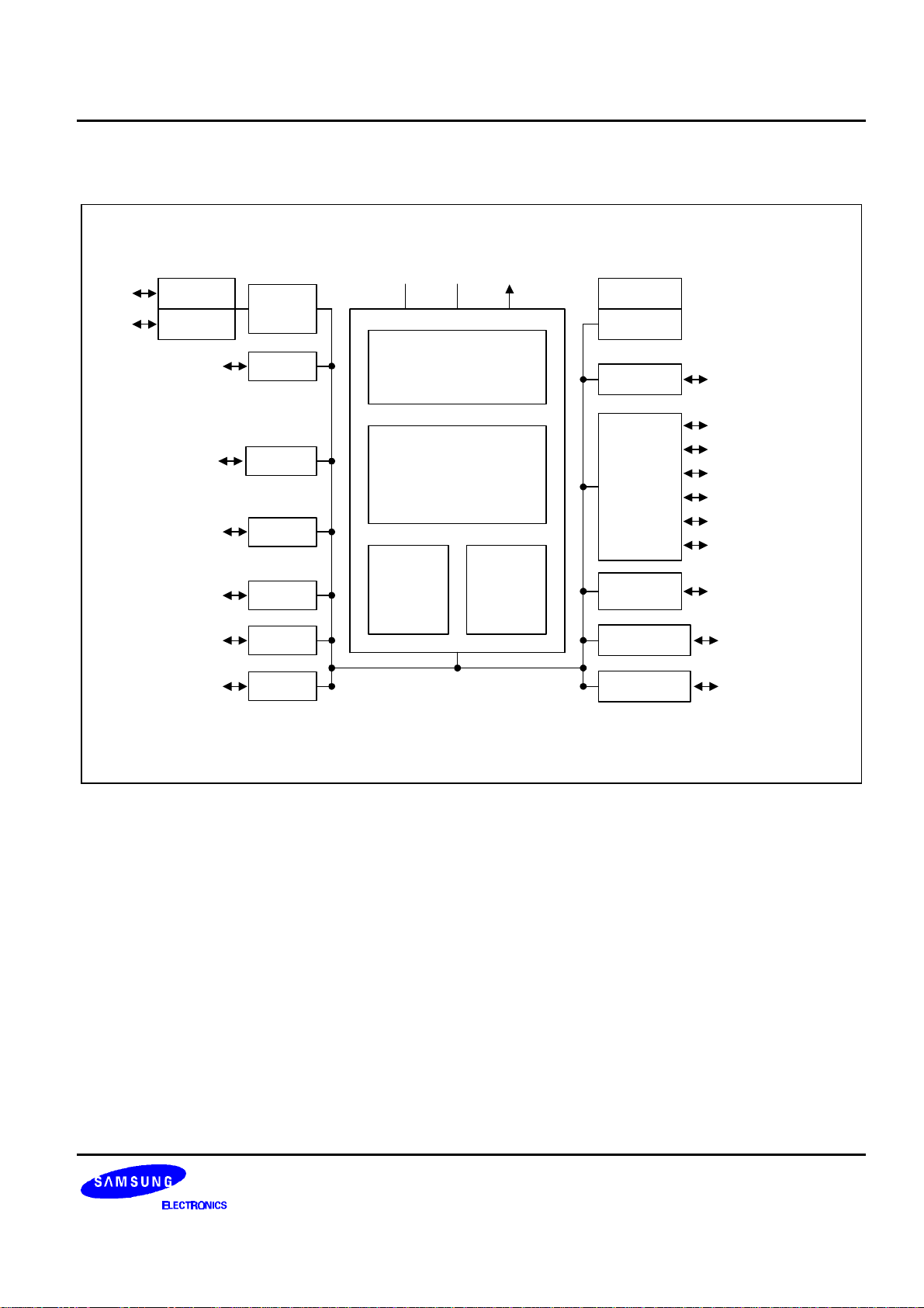
BLOCK DIAGRAM
X
IN
X
TAOUT/
P0.0
T1CLK/
P0.1
8-Bit Timer/
CounterA
8-Bit Timer/
CounterB
P0.0/TAOUT/INT
P0.1/T1CLK/INT
P0.2/INT
P0.3/BUZ/INT
P0.4
P0.5
P1.0/AD0/INT
P1.1/AD1/INT
P1.2/AD2/INT
P1.3/AD3/INT
P2.0/SCK/SEG1
P2.1/SO/SEG0
P2.2/SI
P2.3
P3.0/INTP/SEG3
P3.1/INTP/SEG2
16-Bit
Timer/
Counter1
I/O Port 0
I/O Port 1
I/O Port 2
I/O Port 3
RESET
8-Kbyte
ROM
XT
Port I/O and Interrupt
Control
SAM88RCRI CPU
IN
OUT
XT
OUT
264-Byte
Register
File
Watchdog
Timer
Basic Timer
Watch Timer
LCD
Driver/
Controller
SIO
BUZ/P0.3
COM0-COM3/P6.3-P6.0
COM4-COM7/
SEG19-SEG16/P5.7-P5.4
SEG0-SEG1/P2.1-P2.0
SEG2-SEG3/P3.1-P3.0
SEG4-SEG11/P4.0-P4.7
SEG12-SEG15/P5.0-P5.3
P2.0/SCK/SEG1
P2.1/SO/SEG0
P2.2/SI
P4.0-P4.7/
SEG4-SEG11
P5.0-P5.3/
SEG12-SEG15
P5.4-P5.7/
SEG16-SEG19/
COM7-COM4
I/O Port 4
I/O Port 5
Figure 1-1. Block Diagram
A/D Converter
I/O Port 6 P6.0-P6.3/COM3-COM0
P1.0-P1.3/AD0-AD3
1-3
Page 26

PRODUCT OVERVIEW S3C9228/P9228
PIN ASSIGNMENTS
P0.5
P0.4
P0.3/BUZ/INT
P0.2/INT
P0.1/T1CLK/INT
P0.0/TAOUT/INT
COM0/P6.3
COM1/P6.2
COM2/P6.1
COM3/P6.0
COM4/SEG19/P5.7
4443424140393837363534
P1.0/AD0/INT
P1.1/AD1/INT
P1.2/AD2/INT
P1.3/AD3/INT
VDD
VSS
XOUT
XIN
TEST
XTIN
XTOUT
1
2
3
4
5
6
7
8
9
10
11
S3C9228
(44-QFP)
33
32
31
30
29
28
27
26
25
24
23
COM5/SEG18/P5.6
COM6/SEG17/P5.5
COM7/SEG16/P5.4
SEG15/P5.3
SEG14/P5.2
SEG13/P5.1
SEG12/P5.0
SEG11/P4.7
SEG10/P4.6
SEG9/P4.5
SEG8/P4.4
1213141516171819202122
P2.3
RESET
P2.2/SI
SEG4/P4.0
SEG5/P4.1
SEG6/P4.2
SEG7/P4.3
SEG0/P2.1/SO
SEG1/P2.0/SCK
SEG2/P3.1/INTP
SEG3/P3.0/INTP
Figure 1-2. S3C9228 44-QFP Pin Assignments
1-4
Page 27

S3C9228/P9228 PRODUCT OVERVIEW
COM1/P6.2
COM0/P6.3
P0.0/TAOUT/INT
P0.1/T1CLK/INT
P0.2/INT
P0.3/BUZ/INT
P1.0/AD0/INT
P1.1/AD1/INT
P1.2/AD2/INT
P1.3/AD3/INT
V
DD
V
X
OUT
X
TEST
XT
XT
OUT
RESET
P2.3
P2.2/SI
SEG0/P2.1/SO
Figure 1-3. S3C9228 42-SDIP Pin Assignments
SS
1
2
3
4
5
6
7
8
S3C9228
(42-SDIP)
9
10
11
12
13
IN
14
15
IN
16
17
18
19
20
21
42
41
40
39
38
37
36
35
34
33
32
31
30
29
28
27
26
25
24
23
22
COM2/P6.1
COM3/P6.0
COM4/SEG19/P5.7
COM5/SEG18/P5.6
COM6/SEG17/P5.5
COM7/SEG16/P5.4
SEG15/P5.3
SEG14/P5.2
SEG13/P5.1
SEG12/P5.0
SEG11/P4.7
SEG10/P4.6
SEG9/P4.5
SEG8/P4.4
SEG7/P4.3
SEG6/P4.2
SEG5/P4.1
SEG4/P4.0
SEG3/P3.0/INTP
SEG2/P3.1/INTP
SEG1/P2.0/SCK
1-5
Page 28
PRODUCT OVERVIEW S3C9228/P9228
PIN DESCRIPTIONS
Table 1-1. Pin Descriptions
Pin Names Pin
Type
P0.0
I/O
P0.1
P0.2
P0.3
P0.4-P0.5
P1.0
O
I/O
P1.1
P1.2
P1.3
P2.0
I/O
P2.1
P2.2
I/O
P2.3
P3.0
I/O
P3.1
1-bit programmable I/O port. Schmitt
trigger input or push-pull, open-drain
output and software assignable pull-ups.
1-bit programmable output port. C 43-44
1-bit programmable I/O port. Schmitt
trigger input or push-pull, open-drain
output and software assignable pull-ups.
1-bit programmable I/O port. Schmitt
trigger input or push-pull, open-drain
output and software assignable pull-ups. E-4 14(20)
1-bit programmable I/O port. Schmitt
trigger input or push-pull, open-drain
Pin Description Circuit
Number
E-4 39(3)
F-16A 1(7)
H-32A 16(22)
H-32B 18(24)
Pin
Numbers
40(4)
41(5)
42(6)
2(8)
3(9)
4(10)
15(21)
13(19)
17(23)
Share
Pins
TAOUT/INT
T1CLK/INT
INT
BUZ/INT
AD0/INT
AD1/INT
AD2/INT
AD3/INT
SCK/SEG1
SO/SEG0
SI
–
INTP/SEG3
INTP/SEG2
output and software assignable pull-ups.
P4.0–P4.7
I/O
1-bit programmable I/O port. Input or
H-32 19-26(25-32) SEG4-SEG11
push-pull, open-drain output and
software assignable pull-ups.
P5.0–P5.3
I/O
1-bit programmable I/O port. Input or
H-32 27-30(33-36) SEG12-SEG15
push-pull, open-drain output and
P5.4–P5.7 software assignable pull-ups. 31-34(37-40) SEG16-SEG19
/COM7-COM4
P6.0-P6.3
I/O
1-bit programmable I/O port. Input or
push-pull, open-drain output and
H-32 35-38
(41-42,1-2)
COM3-COM0
software assignable pull-ups.
NOTE: Parentheses indicate pin number for 42-SDIP-600 package.
1-6
Page 29

S3C9228/P9228 PRODUCT OVERVIEW
Table 1-1. Pin Descriptions (Continued)
Pin Names Pin
Type
VDD, V
X
OUT
XT
OUT
, X
SS
IN
, XT
IN
– Power input pins for internal power block – 5,6(11,12) –
– Main oscillator pins for main clock – 7,8(13,14)
– Sub oscillator pins for sub clock – 11,10(17,16) –
TEST – Chip test input pin
Pin Description Circuit
Number
– 9(15) –
Pin
Numbers
Share
Pins
Hold GND when the device is operating
RESET
I RESET signal input pin. Schmitt trigger
B 12(18) –
input with internal pull-up resistor.
INT I/O External interrupts input. E-4
F-16A
39-42(3-6)
1-4(7-10)
P0.0-P0.3
P1.0-P1.3
INTP I/O Key scan interrupts inputs. H-32B 17-18(23-24) P3.1-P3.0
T1CLK I/O Timer 1/A external clock input. E-4 40(4) P0.1
TAOUT I/O Timer 1/A clock output. E-4 39(3) P0.0
AD0-AD3 I/O Analog input pins for A/D converts
F-16A 1-4(7-10) P1.0-P1.3
module.
BUZ I/O Buzzer signal output. E-4 42(6) P0.3
SCK
SO
I/O Serial clock, serial data output, serial data
input
H-32A 16-15(22-21) P2.0-P2.1
SI E-4 14(20) P2.2
SEG0-SEG1 I/O LCD segment signal output H-32A 15-16(21-22) P2.1-P2.0
SEG2-SEG3 H-32B 17-18(23-24) P3.1-P3.0
SEG4-SEG19 H-32 19-34(25-40) P4.0-P4.7
P5.0-P5.7
COM0-COM7 I/O LCD common signal output H-32 38-31
(2-1,42-37)
P6.3-P6.0
P5.7-P5.4
NOTE: Parentheses indicate pin number for 42-SDIP-600 package.
1-7
Page 30
PRODUCT OVERVIEW S3C9228/P9228
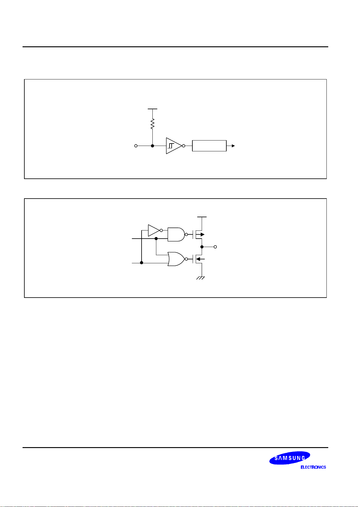
PIN CIRCUIT DIAGRAMS
VDD
Pull-Up
Resistor
RESET
Data
Output
Disable
Noise Filter
Figure 1-4. Pin Circuit Type B
VDD
Output
VSS
Figure 1-5. Pin Circuit Type C
1-8
Page 31

S3C9228/P9228 PRODUCT OVERVIEW
VDD
Pull-up
VDD
Open-Drain
Resistor
Pull-up
Enable
Data
Output
Disable
External
Interrupt
Input
Pull-up Enable
I/O
Figure 1-7. Pin Circuit Type E-4
VDD
Pull-up
Resistor
Open-Drain EN
Data
Output Disable
ADEN
ADSELECT
Data
To ADC
Figure 1-8. Pin Circuit Type F-16A
Circuit
Type E
I/O
1-9
Page 32

PRODUCT OVERVIEW S3C9228/P9228
VLC1
VLC2
VLC3
OutSEG/COM
Output
Disable
VLC4
VLC5
VSS
Figure 1-9. Pin Circuit Type H-23
1-10
Page 33

S3C9228/P9228 PRODUCT OVERVIEW
VDD
Pull-up
VDD
Open-Drain EN
Resistor
Pull-up
Enable
Data
LCD Out EN
COM/SEG
Output
Disable
Open-Drain EN
Circuit
Type H-23
Figure 1-10. Pin Circuit Type H-32
VDD
Pull-up
VDD
Resistor
I/O
Pull-up
Enable
Data
LCD Out EN
COM/SEG
Output
Disable
I/O
Circuit
Type H-23
Figure 1-11. Pin Circuit Type H-32A
1-11
Page 34

PRODUCT OVERVIEW S3C9228/P9228
VDD
Pull-up
VDD
Open-Drain EN
Resistor
Pull-up
Enable
Data
LCD Out EN
COM/SEG
Output
Disable
I/O
Port
Enable
(LMOD.5)
Circuit
Type H-23
Figure 1-12. Pin Circuit Type H-32B
1-12
Page 35

S3C9228/P9228 ADDRESS SPACES
2 ADDRESS SPACES
OVERVIEW
The S3C9228/P9228 microcontroller has three kinds of address space:
— Program memory (ROM)
— Internal register file
— LCD display register file
A 16-bit address bus supports program memory operations. Special instructions and related internal logic
determine when the 16-bit bus carries addresses for program memory. A separate 8-bit register bus carries
addresses and data between the CPU and the internal register file.
The S3C9228 has 8K bytes of mask-programmable program memory on-chip. The S3C9228/P9228
microcontroller has 244 bytes general-purpose registers in its internal register file and the 20 bytes for LCD
display memory is implemented in the internal register file too. Fifty-six bytes in the register file are mapped for
system and peripheral control functions.
2-1
Page 36

ADDRESS SPACES S3C9228/P9228
PROGRAM MEMORY (ROM)
Program memory (ROM) stores program code or table data. The S3C9228 has 8K bytes of mask-programable
program memory. The program memory address range is therefore 0H-1FFFH. The first 2 bytes of the ROM
(0000H–0001H) are an interrupt vector address. The program reset address in the ROM is 0100H.
(Decimal)
8,192
8K bytes
Internal
Program
Memory
Area
256
Program Start
2 0002H
1
0
Interrupt
Vector
(Hex)
1FFFH
0100H
0001H
0000H
2-2
Figure 2-1. S3C9228/P9228 Program Memory Address Space
Page 37

S3C9228/P9228 ADDRESS SPACES
REGISTER ARCHITECTURE
The upper 72 bytes of the S3C9228/P9228's internal register file are addressed as working registers, system
control registers and peripheral control registers. The lower 184 bytes of internal register file (00H–B7H) is called
the general purpose register space.
For many SAM88RCRI microcontrollers, the addressable area of the internal register file is further expanded by
the additional of one or more register pages at general purpose register space (00H–BFH). This register file
expansion is implemented by page 1 in the S3C9228/P9228. The page 1 (20 × 8 bits) is for LCD display register
and can be used as general-purpose registers.
FFH
Peripheral Control
Registers
E0H
72 Bytes of
Common Area
DFH
D0H
CFH
C0H
BFH
B8H
B7H
System Control
Registers
Working Registers
Peripheral Control
Registers
184 Bytes
General Purpose
Register File
and Stack Area
~
64 Bytes
00H
(Page 0)
Figure 2-2. Internal Register File Organization
3FH
13H
00H
General Purpose
Register File
LCD Display
Registers
(Page 1)
2-3
Page 38

ADDRESS SPACES S3C9228/P9228
COMMON WORKING REGISTER AREA (C0H–CFH)
The SAM88RCRI register architecture provides an efficient method of working register addressing that takes full
advantage of shorter instruction formats to reduce execution time.
This16-byte address range is called common area. That is, locations in this area can be used as working registers
by operations that address any location on any page in the register file. Typically, these working registers serve
as temporary buffers for data operations between different pages.
The Register (R) addressing mode can be used to access this area
Registers are addressed either as a single 8-bit register or as a paired 16-bit register. In 16-bit register pairs, the
address of the first 8-bit register is always an even number and the address of the next register is an odd number.
The most significant byte of the 16-bit data is always stored in the even-numbered register; the least significant
byte is always stored in the next (+ 1) odd-numbered register.
MSB
Rn
Figure 2-3. 16-Bit Register Pairs
LSB
Rn + 1
n = Even address
++ PROGRAMMING TIP — Addressing the Common Working Register Area
As the following examples show, you should access working registers in the common area, locations C0H–CFH,
using working register addressing mode only.
Examples: 1. LD 0C2H,40H ; Invalid addressing mode!
Use working register addressing instead:
LD R2,40H ; R2 (C2H) ← the value in location 40H
2. ADD 0C3H,#45H ; Invalid addressing mode!
Use working register addressing instead:
ADD R3,#45H ; R3 (C3H) ← R3 + 45H
2-4
Page 39

S3C9228/P9228 ADDRESS SPACES
SYSTEM STACK
S3C9-series microcontrollers use the system stack for subroutine calls and returns and to store data. The PUSH
and POP instructions are used to control system stack operations. The S3C9228/P9228 architecture supports
stack operations in the internal register file.
STACK OPERATIONS
Return addresses for procedure calls and interrupts and data are stored on the stack. The contents of the PC are
saved to stack by a CALL instruction and restored by the RET instruction. When an interrupt occurs, the contents
of the PC and the FLAGS register are pushed to the stack. The IRET instruction then pops these values back to
their original locations. The stack address is always decremented before a push operation and incremented after
a pop operation. The stack pointer (SP) always points to the stack frame stored on the top of the stack, as shown
in Figure 2-4.
High Address
PCL
PCL
Top of
stack
PCH
Stack contents
after a call
instruction
Top of
stack
Low Address
PCH
Flags
Stack contents
after an
interrupt
Figure 2-4. Stack Operations
STACK POINTER (SP)
Register location D9H contains the 8-bit stack pointer (SP) that is used for system stack operations. After a reset,
the SP value is undetermined.
Because only internal memory space is implemented in the S3C9228/P9228, the SP must be initialized to an 8bit value in the range 00H–B7H.
NOTE
In case a Stack Pointer is initialized to 00H, it is decreased to FFH when stack operation starts. This
means that a Stack Pointer access invalid stack area.
2-5
Page 40

ADDRESS SPACES S3C9228/P9228
++ PROGRAMMING TIP — Standard Stack Operations Using PUSH and POP
The following example shows you how to perform stack operations in the internal register file using PUSH and
POP instructions:
LD SP,#0B8H ; SP ← B8H (Normally, the SP is set to 0B8H by the
•
•
•
PUSH SYM ; Stack address 0B7H ← SYM
PUSH WTCON ; Stack address 0B6H ← WTCON
PUSH 20H ; Stack address 0B5H ← 20H
PUSH R3 ; Stack address 0B4H ← R3
•
•
•
POP R3 ; R3 ← Stack address 0B4H
POP 20H ; 20H ← Stack address 0B5H
POP WTCON ; WTCON ← Stack address 0B6H
POP SYM ; SYM ← Stack address 0B7H
; initialization routine)
2-6
Page 41

S3C9228/P9228 ADDRESSING MODES
3 ADDRESSING MODES
OVERVIEW
Instructions that are stored in program memory are fetched for execution using the program counter. Instructions
indicate the operation to be performed and the data to be operated on. Addressing mode is the method used to
determine the location of the data operand. The operands specified in SAM88RCRI instructions may be condition
codes, immediate data, or a location in the register file, program memory, or data memory.
The SAM88RCRI instruction set supports six explicit addressing modes. Not all of these addressing modes are
available for each instruction. The addressing modes and their symbols are as follows:
— Register (R)
— Indirect Register (IR)
— Indexed (X)
— Direct Address (DA)
— Relative Address (RA)
— Immediate (IM)
3-1
Page 42

ADDRESSING MODES S3C9228/P9228
REGISTER ADDRESSING MODE (R)
In Register addressing mode, the operand is the content of a specified register (see Figure 3-1). Working register
addressing differs from Register addressing because it uses a 16-byte working register space in the register file
and a 4-bit register within that space (see Figure 3-2).
Program Memory Register File
8-bit Register
File Address
One-Operand
Instruction
(Example)
Sample Instruction:
dst
OPCODE
Point to One
OPERAND
Rigister in Register
File
Value used in
Instruction Execution
DEC CNTR ; Where CNTR is the label of an 8-bit register address
4-Bit
Working Register
Two-Operand
Instruction
(Example)
Figure 3-1. Register Addressing
Program Memory
dst
OPCODE
Sample Instruction:
src
4 LSBs
Point to the
Woking Register
(1 of 16)
Register File
CFH
.
.
.
.
OPERAND
C0H
3-2
ADD R1, R2 ; Where R1 = C1H and R2 = C2H
Figure 3-2. Working Register Addressing
Page 43

S3C9228/P9228 ADDRESSING MODES
INDIRECT REGISTER ADDRESSING MODE (IR)
In Indirect Register (IR) addressing mode, the content of the specified register or register pair is the address of
the operand. Depending on the instruction used, the actual address may point to a register in the register file, to
program memory (ROM), or to an external memory space (see Figures 3-3 through 3-6).
You can use any 8-bit register to indirectly address another register. Any 16-bit register pair can be used to
indirectly address another memory location.
Program Memory Register File
8-Bit Register
File Address
One-Operand
Instruction
(Example)
dst
OPCODE
Point to One
ADDRESS
Rigister in Register
File
Address of Operand
used by Instruction
Value used in
Instruction Execution
Sample Instruction:
RL @SHIFT ; Where SHIFT is the label of an 8-Bit register address
OPERAND
Figure 3-3. Indirect Register Addressing to Register File
3-3
Page 44

ADDRESSING MODES S3C9228/P9228
INDIRECT REGISTER ADDRESSING MODE (Continued)
Register File
Program Memory
Example
Instruction
References
Program
Memory
Sample Instructions:
CALL @RR2
JP @RR2
REGISTER
dst
OPCODE
Points to
Rigister Pair
Value used in
Instruction
PAIR
Program Memory
OPERAND
Figure 3-4. Indirect Register Addressing to Program Memory
16-Bit
Address
Points to
Program
Memory
3-4
Page 45

S3C9228/P9228 ADDRESSING MODES
INDIRECT REGISTER ADDRESSING MODE (Continued)
Register File
CFH
.
.
.
.
OPERAND
C0H
4-Bit
Working
Register
Address
Program Memory
dst
OPCODE
src
4 LSBs
Point to the
Woking Register
(1 of 16)
Sample Instruction:
OR R6, @R2
Value used in
Instruction
OPERAND
Figure 3-5. Indirect Working Register Addressing to Register File
3-5
Page 46

ADDRESSING MODES S3C9228/P9228
INDIRECT REGISTER ADDRESSING MODE (Concluded)
Register File
CFH
.
.
.
.
Register
Pair
or
Data Memory
OPERAND
C0H
16-Bit
address
points to
program
memory
or data
memory
4-Bit Working
Register Address
Example Instruction
References either
Program Memory or
Data Memory
Program Memory
dst
OPCODE
src
Next 3 Bits Point
to Working
Register Pair
(1 of 8)
LSB Selects
Value used in
Instruction
Program Memory
3-6
Sample Instructions:
LCD R5,@RR6 ; Program memory access
LDE R3,@RR14 ; External data memory access
LDE @RR4, R8 ; External data memory access
Figure 3-6. Indirect Working Register Addressing to Program or Data Memory
Page 47

S3C9228/P9228 ADDRESSING MODES
INDEXED ADDRESSING MODE (X)
Indexed (X) addressing mode adds an offset value to a base address during instruction execution in order to
calculate the effective operand address (see Figure 3-7). You can use Indexed addressing mode to access
locations in the internal register file or in external memory.
In short offset Indexed addressing mode, the 8-bit displacement is treated as a signed integer in the range of
–128 to +127. This applies to external memory accesses only (see Figure 3-8).
For register file addressing, an 8-bit base address provided by the instruction is added to an 8-bit offset contained
in a working register. For external memory accesses, the base address is stored in the working register pair
designated in the instruction. The 8-bit or 16-bit offset given in the instruction is then added to the base address
(see Figure 3-9).
The only instruction that supports Indexed addressing mode for the internal register file is the Load instruction
(LD). The LDC and LDE instructions support Indexed addressing mode for internal program memory, external
program memory, and for external data memory, when implemented.
Register File
Two-Operand
Instruction
Example
Sample Instruction:
LD R0, #BASE[R1] ; Where BASE is an 8-bit immediate value
~ ~
Value used in
Instruction
+
Program Memory
Base Address
dst
OPCODE
src
Figure 3-7. Indexed Addressing to Register File
4 LSBs
Point to One of the
Woking Register
(1 of 16)
OPERAND
~ ~
INDEX
3-7
Page 48

ADDRESSING MODES S3C9228/P9228
INDEXED ADDRESSING MODE (Continued)
4-Bit Working
Register Address
Sample Instructions:
LDC R4, #04H[RR2] ; The values in the program address (RR2 + #04H)
LDE R4,#04H[RR2] ; Identical operation to LDC example, except that
Program Memory
XS (OFFSET)
dst
OPCODE
src
NEXT 3 Bits
Point to Working
Register Pair
(1 of 8)
LSB Selects
+
8-Bits
16-Bits
Register File
Register
Pair
16-Bits
Program Memory
or
Data Memory
OPERAND
are loaded into register R4.
external program memory is accessed.
16-Bit
address
added to
offset
Value used in
Instruction
3-8
Figure 3-8. Indexed Addressing to Program or Data Memory with Short Offset
Page 49

S3C9228/P9228 ADDRESSING MODES
INDEXED ADDRESSING MODE (Concluded)
4-Bit Working
Register Address
Sample Instructions:
LDC R4, #1000H[RR2] ; The values in the program address (RR2 +
#1000H)
LDE R4, #1000H[RR2] ; Identical operation to LDC example, except that
Program Memory
XLH (OFFSET)
XLL (OFFSET)
dst src
OPCODE
NEXT 3 Bits
Point to Working
Register Pair
(1 of 8)
LSB Selects
+
8-Bits
16-Bits
Register File
Register
Pair
16-Bits
Program Memory
or
Data Memory
OPERAND
are loaded into register R4.
external program memory is accessed.
Value used in
Instruction
16-Bit
address
added to
offset
Figure 3-9. Indexed Addressing to Program or Data Memory with Long Offset
3-9
Page 50

ADDRESSING MODES S3C9228/P9228
DIRECT ADDRESS MODE (DA)
In Direct Address (DA) mode, the instruction provides the operand's 16-bit memory address. Jump (JP) and Call
(CALL) instructions use this addressing mode to specify the 16-bit destination address that is loaded into the PC
whenever a JP or CALL instruction is executed.
The LDC and LDE instructions can use Direct Address mode to specify the source or destination address for
Load operations to program memory (LDC) or to external data memory (LDE), if implemented.
Program or
Data Memory
Memory
Program Memory
Address
Used
Upper Address Byte
Lower Address Byte
dst/src
Sample Instructions:
LDC R5,1234H ; The values in the program address (1234H)
LDE R5,1234H ; Identical operation to LDC example, except that
"0" or "1"
OPCODE
are loaded into register R5.
external program memory is accessed.
LSB Selects Program
Memory or Data Memory:
"0" = Program Memory
"1" = Data Memory
Figure 3-10. Direct Addressing for Load Instructions
3-10
Page 51

S3C9228/P9228 ADDRESSING MODES
DIRECT ADDRESS MODE (Continued)
Program Memory
Next OPCODE
Program
Memory
Address
Used
Lower Address Byte
Upper Address Byte
OPCODE
Sample Instructions:
JP C,JOB1 ; Where JOB1 is a 16-bit immediate address
CALL DISPLAY ; Where DISPLAY is a 16-bit immediate address
Figure 3-11. Direct Addressing for Call and Jump Instructions
3-11
Page 52

ADDRESSING MODES S3C9228/P9228
RELATIVE ADDRESS MODE (RA)
In Relative Address (RA) mode, a two's-complement signed displacement between – 128 and + 127 is specified
in the instruction. The displacement value is then added to the current PC value. The result is the address of the
next instruction to be executed. Before this addition occurs, the PC contains the address of the instruction
immediately following the current instruction.
The instructions that support RA addressing is JR.
Program Memory
Next OPCODE
Program Memory
Address Used
Current
Current Instruction
Displacement
OPCODE
PC Value
Signed
Displacement Value
+
Sample Instructions:
JR ULT,$ + OFFSET ; Where OFFSET is a value in the range + 127 to - 128
Figure 3-12. Relative Addressing
IMMEDIATE MODE (IM)
In Immediate (IM) addressing mode, the operand value used in the instruction is the value supplied in the
operand field itself. Immediate addressing mode is useful for loading constant values into registers.
Program Memory
OPERAND
OPCODE
(The Operand value is in the instruction)
Sample Instruction:
LD R0,#0AAH
3-12
Figure 3-13. Immediate Addressing
Page 53

S3C9228/P9228 CONTROL REGISTERS
4 CONTROL REGISTERS
OVERVIEW
In this section, detailed descriptions of the S3C9228/P9228 control registers are presented in an easy-to-read
format. These descriptions will help familiarize you with the mapped locations in the register file. You can also
use them as a quick-reference source when writing application programs.
System and peripheral registers are summarized in Table 4-1. Figure 4-1 illustrates the important features of the
standard register description format.
Control register descriptions are arranged in alphabetical order according to register mnemonic. More information
about control registers is presented in the context of the various peripheral hardware descriptions in Part II of this
manual.
4-1
Page 54

CONTROL REGISTERS S3C9228/P9228
Table 4-1. System and Peripheral Control Registers (Page 0)
Register Name Mnemonic Address (Page 0) R/W
Decimal Hex
Port 0 Control Register P0CON 235 EBH
Port 0 Pull-up Resistor Enable Register P0PUR 236 ECH
Port 0 Interrupt Control Register P0INT 237 EDH
Port 0 Interrupt Edge Selection Register P0EDGE 238 EEH
Port 1 Control Register P1CON 239 EFH
Port 1 Pull-up Resistor Enable Register P1PUR 240 F0H
Port 1 Interrupt Control Register P1INT 241 F1H
Port 1 Interrupt Edge Selection Register P1EDGE 242 F2H
Port 2 Control Register P2CON 243 F3H
Port 2 Pull-up Resistor Enable Register P2PUR 244 F4H
Port 3 Control Register P3CON 245 F5H
Port 3 Pull-up Resistor Enable Register P3PUR 246 F6H
Port 3 Interrupt Control Register P3INT 247 F7H
Port 3 Interrupt Edge Selection Register P3EDGE 248 F8H
Port 4 Control Register (High Byte) P4CONH 249 F9H
Port 4 Control Register (Low Byte) P4CONL 250 FAH
Port 5 Control Register (High Byte) P5CONH 251 FBH
Port 5 Control Register (Low Byte) P5CONL 252 FCH
Port 6 Control Register P6CON 253 FDH
LCD Mode Register LMOD 254 FEH
R/W
R/W
R/W
R/W
R/W
R/W
R/W
R/W
R/W
R/W
R/W
R/W
R/W
R/W
R/W
R/W
R/W
R/W
R/W
R/W
Location FFH is not mapped.
4-2
Page 55

S3C9228/P9228 CONTROL REGISTERS
Table 4-1. System and Peripheral Control Registers (Page 0)
Register Name Mnemonic Address (Page 0) R/W
Decimal Hex
Locations D8H-B9H are not mapped.
Timer B Control Register
Timer 1/A Control Register
Timer B Data Register
Timer A Data Register
Timer B Counter
Timer A Counter
A/D Converter Control Register
A/D Converter Data Register (High Byte)
A/D Converter Data Register (Low Byte)
Oscillator Control Register
System Clock Control Register
System Flags Register
Interrupt Pending Register 1
Interrupt Pending Register 2
LCD Port Control Register
Stack Pointer
Watch Timer Control Register
TBCON 202
TACON 203
TBDATA 204
TADATA 205
TBCNT 206
TACNT 207
ADCON 208
ADDATAH 209
ADDATAL 210
OSCCON 211
CLKCON 212
FLAGS 213
INTPND1 214
INTPND2 215
LPOT 216
SP 217
WTCON 218
BAH R/W
BBH R/W
BCH R/W
BDH R/W
BEH R
BFH R
D0H R/W
D1H R/W
D2H R/W
D3H R/W
D4H R/W
D5H R/W
D6H R/W
D7H R/W
D8H R/W
D9H R/W
DAH R/W
Location DBH is not mapped.
Basic Timer Control Register BTCON 220 DCH R/W
Basic Timer Counter BTCNT 221 DDH R
Location DEH is not mapped.
System Mode Register SYM 223 DFH R/W
STOP Control Register STPCON 224 E0H R/W
SIO Control Register SIOCON 225 E1H R/W
SIO Data Register SIODATA 226 E2H R/W
SIO Prescaler Register SIOPS 227 E3H R/W
Port 0 Data Register P0 228 E4H R/W
Port 1 Data Register P1 229 E5H R/W
Port 2 Data Register P2 230 E6H R/W
Port 3 Data Register P3 231 E7H R/W
Port 4 Data Register P4 232 E8H R/W
Port 5 Data Register P5 233 E9H R/W
Port 6 Data Register P6 234 EAH R/W
4-3
Page 56

CONTROL REGISTERS S3C9228/P9228
Bit number(s) that is/are appended to the
register name for bit addressing
Register
mnemonic
Full Register name
Name of individual
bit or bit function
Register address
(hexadecimal)
FLAGS - System Flags Register
Bit Identifier
RESET RESET Value
Read/Write
.7
.6
.5
R = Read-only
W = Write-only
R/W = Read/write
' - ' = Not used
Addressing mode or
modes you can use to
modify register values
.7 .6 .5 .4 .2.3 .1 .0
x
R/WxR/W
Carry Flag (C)
0 Operation dose not generate a carry or borrow condition
1 Operation generates carry-out or borrow into high-order bit7
Zero Flag
0 Operation result is a non-zero value
1 Operation result is zero
Sign Flag
0 Operation generates positive number (MSB = "0")
1 Operation generates negative number (MSB = "1")
x
R/W
Description of the
effect of specific
bit settings
x
R/W
D5H
x
R/W
x
R/W
RESET value notation:
'-' = Not used
'x' = Undetermind value
'0' = Logic zero
'1' = Logic one
0
R/W
0
R/W
Bit number:
MSB = Bit 7
LSB = Bit 0
4-4
Figure 4-1. Register Description Format
Page 57

S3C9228/P9228 CONTROL REGISTERS
ADCON — A/D Converter Control Register D0H
Bit Identifier .7 .6 .5 .4 .3 .2 .1 .0
RESETRESET Value
Read/Write
– – 0 0 0 0 0 0
– – R/W R/W R R/W R/W R/W
.7-.6
.5-.4 A/D Input Pin Selection Bits
.3 End of Conversion Bit (Read-only)
.2-.1 Clock Source Selection Bits
Not used for the S3C9228/P9228
0 0 AD0 (P1.0)
0 1 AD1 (P1.1)
1 0 AD2 (P1.2)
1 1 AD3 (P1.3)
0 Conversion not complete
1 Conversion complete
0 0 fxx/16
0 1 fxx/8
1 0 fxx/4
1 1 fxx
.0 Start or Enable Bit
0 Disable operation
1 Start operation (automatically disable operation after conversion complete)
4-5
Page 58

CONTROL REGISTERS S3C9228/P9228
BTCON — Basic Timer Control Register DCH
Bit Identifier .7 .6 .5 .4 .3 .2 .1 .0
RESETRESET Value
Read/Write
.7-.4 Watchdog Timer Enable Bits
.3-.2 Basic Timer Input Clock Selection Bits
0 0 0 0 0 0 0 0
R/W R/W R/W R/W R/W R/W R/W R/W
1 0 1 0 Disable watchdog function
Any other value Enable watchdog function
0 0 fxx/4096
0 1 fxx/1024
1 0 fxx/128
1 1 fxx/16
.1
Basic Timer Counter Clear Bit
(1)
0 No effect
1 Clear the basic timer counter value (BTCNT)
.0
Clock Frequency Divider Clear Bit for Basic Timer and Timer/Counters
(2)
0 No effect
1 Clear clock frequency dividers
NOTES
1. When "1" is written to BTCON.1, the basic timer counter value is cleared to "00H". Immediately following the write
operation, the BTCON.1 value is automatically cleared to "0".
2. When "1" is written to BTCON.0, the corresponding frequency divider is cleared to "00H". Immediately following the
write operation, the BTCON.0 value is automatically cleared to "0".
4-6
Page 59

S3C9228/P9228 CONTROL REGISTERS
CLKCON — System Clock Control Register D4H
Bit Identifier .7 .6 .5 .4 .3 .2 .1 .0
RESETRESET Value
Read/Write
.7 Oscillator IRQ Wake-up Function Bit
.6-.5 Bits 6-5
.4-.3 CPU Clock (System Clock) Selection Bits
0 0 0 0 0 0 0 0
R/W R/W R/W R/W R/W R/W R/W R/W
0 Enable IRQ for main or sub oscillator wake-up in power down mode
1 Disable IRQ for main or sub oscillator wake-up in power down mode
0 Always logic zero
0 0 Divide by 16 (fxx/16)
0 1 Divide by 8 (fxx /8)
1 0 Divide by 2 (fxx /2)
1 1 Non-divided clock (fxx)
.2-.0 Bits 2-0
0 Always logic zero
4-7
Page 60

CONTROL REGISTERS S3C9228/P9228
FLAGS — System Flags Register D5H
Bit Identifier .7 .6 .5 .4 .3 .2 .1 .0
RESETRESET Value
Read/Write
.7 Carry Flag (C)
.6 Zero Flag (Z)
.5 Sign Flag (S)
x x x x – – – –
R/W R/W R/W R/W – – – –
0
Operation does not generate a carry or borrow condition
0
Operation result is a non-zero value
1
Operation result is zero
0
Operation generates a positive number (MSB = "0")
1
Operation generates a negative number (MSB = "1")
.4 Overflow Flag (V)
0
Operation result is ≤ +127 or ≥ –128
1
Operation result is ≥ +127 or ≤ –128
.3-.0
Not used for S3C9228/P9228
4-8
Page 61

S3C9228/P9228 CONTROL REGISTERS
INTPND1 — Interrupt Pending Register 1 D6H
Bit Identifier .7 .6 .5 .4 .3 .2 .1 .0
RESETRESET Value
Read/Write
.7 P1.3's Interrupt Pending Bit
.6 P1.2's Interrupt Pending Bit
.5 P1.1's Interrupt Pending Bit
0 0 0 0 0 0 0 0
R/W R/W R/W R/W R/W R/W R/W R/W
0 No interrupt pending (when read), clear pending bit (when write)
1 Interrupt is pending (when read)
0 No interrupt pending (when read), clear pending bit (when write)
1 Interrupt is pending (when read)
0 No interrupt pending (when read), clear pending bit (when write)
1 Interrupt is pending (when read)
.4 P1.0's Interrupt Pending Bit
0 No interrupt pending (when read), clear pending bit (when write)
1 Interrupt is pending (when read)
.3 P0.3's Interrupt Pending Bit
No interrupt pending (when read), Clear pending bit (when write)
0
Interrupt is pending (when read)
1
.2 P0.2's Interrupt Pending Bit
No interrupt pending (when read), Clear pending bit (when write)
0
Interrupt is pending (when read)
1
.1 P0.1's Interrupt Pending Bit
No interrupt pending (when read), Clear pending bit (when write)
0
Interrupt is pending (when read)
1
.0 P0.0's Interrupt Pending Bit
No interrupt pending (when read), Clear pending bit (when write)
0
Interrupt is pending (when read)
1
NOTE: Refer to Page 5-6 to clear any pending bits.
4-9
Page 62

CONTROL REGISTERS S3C9228/P9228
INTPND2 — Interrupt Pending Register 2 D7H
Bit Identifier .7 .6 .5 .4 .3 .2 .1 .0
RESETRESET Value
Read/Write
– – 0 0 0 0 0 0
– – R/W R/W R/W R/W R/W R/W
.7-.6
.5 P3.1 (INTP) Interrupt Pending Bit
.4 P3.0 (INTP) Interrupt Pending Bit
.3 Watch Timer Interrupt Pending Bit
.2 SIO Interrupt Pending Bit
Not used for S3C9228/P9228
0 No interrupt pending (when read), clear pending bit (when write)
1 Interrupt is pending (when read)
0 No interrupt pending (when read), clear pending bit (when write)
1 Interrupt is pending (when read)
No interrupt pending (when read), Clear pending bit (when write)
0
Interrupt is pending (when read)
1
No interrupt pending (when read), Clear pending bit (when write)
0
Interrupt is pending (when read)
1
.1 Timer B Interrupt Pending Bit
No interrupt pending (when read), Clear pending bit (when write)
0
Interrupt is pending (when read)
1
.0 Timer 1/A Interrupt Pending Bit
No interrupt pending (when read), Clear pending bit (when write)
0
Interrupt is pending (when read)
1
NOTE: Refer to Page 5-6 to clear any pending bits.
4-10
Page 63

S3C9228/P9228 CONTROL REGISTERS
LMOD — LCD Mode Control Register FEH
Bit Identifier .7 .6 .5 .4 .3 .2 .1 .0
RESETRESET Value
Read/Write
– 0 0 0 0 0 0 0
– R/W R/W R/W R/W R/W R/W R/W
.7
.6 COM Pins High Impedance Control Bit
.5 Port3 High Impedance Control Bit
.4 LCD Display Control Bit
.3-.2 LCD Duty and Bias Selection Bits
Not used for S3C9228/P9228
0 Normal COMs signal output
1 COM pins are at high impedance
0 Normal I/O
1 High impedance input
Display off (cut off the LCD voltage dividing resistors)
0
Normal display on
1
0 0 1/3 duty, 1/3 bias; COM0–COM2/SEG0–SEG19
0 1 1/4 duty, 1/3 bias; COM0–COM3/SEG0–SEG19
1 0 1/8 duty, 1/4 bias; COM0–COM7/SEG0–SEG15
1 1 1/8 duty, 1/5 bias; COM0–COM7/SEG0–SEG15
.1-.0 LCD Clock Selection Bits
0 0
0 1
1 0
1 1
fw/27 (256 Hz when fw is 32.768 kHz)
fw/26 (512 Hz when fw is 32.768 kHz)
fw/25 (1,024 Hz when fw is 32.768 kHz)
fw/24 (2,048 Hz when fw is 32.768 kHz)
4-11
Page 64

CONTROL REGISTERS S3C9228/P9228
LPOT — LCD Port Control Register D8H
Bit Identifier .7 .6 .5 .4 .3 .2 .1 .0
RESETRESET Value
Read/Write
– 0 0 0 0 0 0 0
– R/W R/W R/W R/W R/W R/W R/W
.7
.6-.4 SEG4-SEG19 and COM0-COM3 Selection Bit
.3 SEG3/P3.0 Selection Bit
.2 SEG2/P3.1 Selection Bit
Not used for S3C9228/P9228
SEG4-7 SEG8-11 SEG12-15 SEG16-19/
P4.0-P4.3 P4.4-P4.7 P5.0-P5.3 P5.4-P5.7 P6.0-P6.3
0 0 0 SEG SEG SEG SEG/COM COM
0 0 1 Port SEG SEG SEG/COM COM
0 1 0 Port Port SEG SEG/COM COM
0 1 1 Port Port Port SEG/COM COM
1 0 0 Port Port Port Port COM
1 0 1 Port Port Port Port Port
0 SEG port
1 Normal I/O port
0 SEG port
1 Normal I/O port
COM0-3
COM7-COM4
.1 SEG1/P2.0 Selection Bit
0 SEG port
1 Normal I/O port
.0 SEG0/P2.1 Selection Bit
0 SEG port
1 Normal I/O port
NOTE: SEG16-SEG19 are shared with COM4-COM7.
4-12
Page 65

S3C9228/P9228 CONTROL REGISTERS
OSCCON — Oscillator Control Register D3H
Bit Identifier .7 .6 .5 .4 .3 .2 .1 .0
RESETRESET Value
Read/Write
– – – – 0 0 – 0
– – – – R/W R/W – R/W
.7-.4
.3 Main Oscillator Control Bit
.2 Sub Oscillator Control Bit
.1
.0 System Clock Selection Bit
Not used for S3C9228/P9228
0 Main oscillator RUN
1 Main oscillator STOP
0 Sub oscillator RUN
1 Sub oscillator STOP
Not used for S3C9228/P9228
0 Select main oscillator for system clock
1 Select sub oscillator for system clock
4-13
Page 66

CONTROL REGISTERS S3C9228/P9228
P0CON – Port 0 Control Register EBH
Bit Identifier .7 .6 .5 .4 .3 .2 .1 .0
RESETRESET Value
Read/Write
.7-.6 P0.3/BUZ/INT Configuration Bits
.5-.4 P0.2/INT Configuration Bits
0 0 0 0 0 0 0 0
R/W R/W R/W R/W R/W R/W R/W R/W
0 0 Schmitt trigger input
0 1 Push-pull output
1 0 N-channel open-drain output
1 1 Alternative function (BUZ output)
0 0 Schmitt trigger input
0 1 Push-pull output
1 0 N-channel open-drain output
1 1 Not available
.3-.2 P0.1/T1CLK/INT Configuration Bits
0 0 Schmitt trigger input (T1CLK input)
0 1 Push-pull output
1 0 N-channel open-drain output
1 1 Not available
.1-.0 P0.0/TAOUT/INT Configuration Bits
0 0 Schmitt trigger input
0 1 Push-pull output
1 0 N-channel open-drain output
1 1 Alternative function (TAOUT output)
4-14
Page 67

S3C9228/P9228 CONTROL REGISTERS
P0INT –Port 0 Interrupt Enable Register EDH
Bit Identifier .7 .6 .5 .4 .3 .2 .1 .0
RESETRESET Value
Read/Write
– – – – 0 0 0 0
– – – – R/W R/W R/W R/W
.7-.4
.3
.2
.1
.0
Not used for S3C9228/P9228
P0.3's Interrupt Enable Bit
0 Disable interrupt
1 Enable interrupt
P0.2's Interrupt Enable Bit
0 Disable interrupt
1 Enable interrupt
P0.1's Interrupt Enable Bit
0 Disable interrupt
1 Enable interrupt
P0.0's Interrupt Enable Bit
0 Disable interrupt
1 Enable interrupt
4-15
Page 68

CONTROL REGISTERS S3C9228/P9228
P0PUR –Port 0 Pull-up Resistors Enable Register ECH
Bit Identifier .7 .6 .5 .4 .3 .2 .1 .0
RESETRESET Value
Read/Write
– – – – 0 0 0 0
– – – – R/W R/W R/W R/W
.7-.4
.3
.2
.1
.0
Not used for S3C9228/P9228
P0.3's Pull-up Resistor Enable Bit
0 Disable pull-up resistor
1 Enable pull-up resistor
P0.2's Pull-up Resistor Enable Bit
0 Disable pull-up resistor
1 Enable pull-up resistor
P0.1's Pull-up Resistor Enable Bit
0 Disable pull-up resistor
1 Enable pull-up resistor
P0.0's Pull-up Resistor Enable Bit
0 Disable pull-up resistor
1 Enable pull-up resistor
4-16
Page 69

S3C9228/P9228 CONTROL REGISTERS
P0EDGE –Port 0 Interrupt Edge Selection Register EEH
Bit Identifier .7 .6 .5 .4 .3 .2 .1 .0
RESETRESET Value
Read/Write
– – – – 0 0 0 0
– – – – R/W R/W R/W R/W
.7-.4
.3
.2
.1
.0
Not used for S3C9228/P9228
P0.3's Interrupt Edge Setting Bit
0 Falling edge interrupt
1 Rising edge interrupt
P0.2's Interrupt State Setting Bit
0 Falling edge interrupt
1 Rising edge interrupt
P0.1's Interrupt State Setting Bit
0 Falling edge interrupt
1 Rising edge interrupt
P0.0's Interrupt State Setting Bit
0 Falling edge interrupt
1 Rising edge interrupt
4-17
Page 70

CONTROL REGISTERS S3C9228/P9228
P1CON – Port 1 Control Register EFH
Bit Identifier .7 .6 .5 .4 .3 .2 .1 .0
RESETRESET Value
Read/Write
.7-.6 P1.3/AD3/INT Configuration Bits
.5-.4 P1.2/AD2/INT Configuration Bits
0 0 0 0 0 0 0 0
R/W R/W R/W R/W R/W R/W R/W R/W
0 0 Schmitt trigger input
0 1 Push-pull output
1 0 N-channel open-drain output
1 1 Alternative function (ADC mode)
0 0 Schmitt trigger input
0 1 Push-pull output
1 0 N-channel open-drain output
1 1 Alternative function (ADC mode)
.3-.2 P1.1/AD1/INT Configuration Bits
0 0 Schmitt trigger input
0 1 Push-pull output
1 0 N-channel open-drain output
1 1 Alternative function (ADC mode)
.1-.0 P1.0/AD0/INT Configuration Bits
0 0 Schmitt trigger input
0 1 Push-pull output
1 0 N-channel open-drain output
1 1 Alternative function (ADC mode)
4-18
Page 71

S3C9228/P9228 CONTROL REGISTERS
P1INT –Port 1 Interrupt Enable Register F1H
Bit Identifier .7 .6 .5 .4 .3 .2 .1 .0
RESETRESET Value
Read/Write
– – – – 0 0 0 0
– – – – R/W R/W R/W R/W
.7-.4
.3
.2
.1
.0
Not used for S3C9228/P9228
P1.3's Interrupt Enable Bit
0 Disable interrupt
1 Enable interrupt
P1.2's Interrupt Enable Bit
0 Disable interrupt
1 Enable interrupt
P1.1's Interrupt Enable Bit
0 Disable interrupt
1 Enable interrupt
P1.0's Interrupt Enable Bit
0 Disable interrupt
1 Enable interrupt
4-19
Page 72

CONTROL REGISTERS S3C9228/P9228
P1PUR –Port 1 Pull-up Resistors Enable Register F0H
Bit Identifier .7 .6 .5 .4 .3 .2 .1 .0
RESETRESET Value
Read/Write
– – – – 0 0 0 0
– – – – R/W R/W R/W R/W
.7-.4
.3
.2
.1
.0
Not used for S3C9228/P9228
P1.3's Pull-up Resistor Enable Bit
0 Disable pull-up resistor
1 Enable pull-up resistor
P1.2's Pull-up Resistor Enable Bit
0 Disable pull-up resistor
1 Enable pull-up resistor
P1.1's Pull-up Resistor Enable Bit
0 Disable pull-up resistor
1 Enable pull-up resistor
P1.0's Pull-up Resistor Enable Bit
0 Disable pull-up resistor
1 Enable pull-up resistor
4-20
Page 73

S3C9228/P9228 CONTROL REGISTERS
P1EDGE –Port 1 Interrupt Edge Selection Register F2H
Bit Identifier .7 .6 .5 .4 .3 .2 .1 .0
RESETRESET Value
Read/Write
– – – – 0 0 0 0
– – – – R/W R/W R/W R/W
.7-.4
.3
.2
.1
.0
Not used for S3C9228/P9228
P1.3's Interrupt Edge Setting Bit
0 Falling edge interrupt
1 Rising edge interrupt
P1.2's Interrupt State Setting Bit
0 Falling edge interrupt
1 Rising edge interrupt
P1.1's Interrupt State Setting Bit
0 Falling edge interrupt
1 Rising edge interrupt
P1.0's Interrupt State Setting Bit
0 Falling edge interrupt
1 Rising edge interrupt
4-21
Page 74

CONTROL REGISTERS S3C9228/P9228
P2CON – Port 2 Control Register F3H
Bit Identifier .7 .6 .5 .4 .3 .2 .1 .0
RESETRESET Value
Read/Write
.7-.6 P2.3 Configuration Bits
.5-.4 P2.2/SI Configuration Bits
0 0 0 0 0 0 0 0
R/W R/W R/W R/W R/W R/W R/W R/W
0 0 Schmitt trigger input
0 1 Push-pull output
1 0 N-channel open-drain output
1 1 Not available
0 0 Schmitt trigger input (SI)
0 1 Push-pull output
1 0 N-channel open-drain output
1 1 Not available
.3-.2 P2.1/SO Configuration Bits
0 0 Schmitt trigger input
0 1 Push-pull output
1 0 N-channel open-drain output
1 1 Alternative function (SO out)
.1-.0 P2.0/SCK Configuration Bits
0 0 Schmitt trigger input (SCK in)
0 1 Push-pull output
1 0 N-channel open-drain output
1 1 Alternative function (SCK out)
4-22
Page 75

S3C9228/P9228 CONTROL REGISTERS
P2PUR –Port 2 Pull-up Resistors Enable Register F4H
Bit Identifier .7 .6 .5 .4 .3 .2 .1 .0
RESETRESET Value
Read/Write
– – – – 0 0 0 0
– – – – R/W R/W R/W R/W
.7-.4
.3
.2
.1
.0
Not used for S3C9228/P9228
P2.3's Pull-up Resistor Enable Bit
0 Disable pull-up resistor
1 Enable pull-up resistor
P2.2's Pull-up Resistor Enable Bit
0 Disable pull-up resistor
1 Enable pull-up resistor
P2.1's Pull-up Resistor Enable Bit
0 Disable pull-up resistor
1 Enable pull-up resistor
P2.0's Pull-up Resistor Enable Bit
0 Disable pull-up resistor
1 Enable pull-up resistor
4-23
Page 76

CONTROL REGISTERS S3C9228/P9228
P3CON – Port 3 Control Register F5H
Bit Identifier .7 .6 .5 .4 .3 .2 .1 .0
RESETRESET Value
Read/Write
– – – – 0 0 0 0
– – – – R/W R/W R/W R/W
.7-.4
.3-.2 P3.1/SEG2/INTP Configuration Bits
.1-.0 P3.0/SEG3/INTP Configuration Bits
Not used for S3C9228/P9228
0 0 Schmitt trigger input
0 1 Push-pull output
1 0 N-channel open-drain output
1 1 Not available
0 0 Schmitt trigger input
0 1 Push-pull output
1 0 N-channel open-drain output
1 1 Not available
4-24
Page 77

S3C9228/P9228 CONTROL REGISTERS
P3INT –Port 3 Interrupt Enable Register F7H
Bit Identifier .7 .6 .5 .4 .3 .2 .1 .0
RESETRESET Value
Read/Write
– – – – – – 0 0
– – – – – – R/W R/W
.7-.2
.1
.0
Not used for S3C9228/P9228
P3.1's Interrupt Enable Bit
0 Disable interrupt
1 Enable interrupt
P3.0's Interrupt Enable Bit
0 Disable interrupt
1 Enable interrupt
4-25
Page 78

CONTROL REGISTERS S3C9228/P9228
P3PUR –Port 3 Pull-up Resistors Enable Register F6H
Bit Identifier .7 .6 .5 .4 .3 .2 .1 .0
RESETRESET Value
Read/Write
– – – – – – 0 0
– – – – – – R/W R/W
.7-.2
.1
.0
Not used for S3C9228/P9228
P3.1's Pull-up Resistor Enable Bit
0 Disable pull-up resistor
1 Enable pull-up resistor
P3.0's Pull-up Resistor Enable Bit
0 Disable pull-up resistor
1 Enable pull-up resistor
4-26
Page 79

S3C9228/P9228 CONTROL REGISTERS
P3EDGE –Port 3 Interrupt Edge Selection Register F8H
Bit Identifier .7 .6 .5 .4 .3 .2 .1 .0
RESETRESET Value
Read/Write
– – – – – – 0 0
– – – – – – R/W R/W
.7-.4
.1
.0
Not used for S3C9228/P9228
P3.1's Interrupt State Setting Bit
0 Falling edge interrupt
1 Rising edge interrupt
P3.0's Interrupt State Setting Bit
0 Falling edge interrupt
1 Rising edge interrupt
4-27
Page 80

CONTROL REGISTERS S3C9228/P9228
P4CONH – Port 4 Control Register High Byte F9H
Bit Identifier .7 .6 .5 .4 .3 .2 .1 .0
RESETRESET Value
Read/Write
.7-.6 P4.7/SEG11 Configuration Bits
.5-.4 P4.6/SEG10 Configuration Bits
0 0 0 0 0 0 0 0
R/W R/W R/W R/W R/W R/W R/W R/W
0 0 Input mode
0 1 Push-pull output
1 0 N-channel open-drain output
1 1 Input, pull-up mode
0 0 Input mode
0 1 Push-pull output
1 0 N-channel open-drain output
1 1 Input, pull-up mode
.3-.2 P4.5/SEG9 Configuration Bits
0 0 Input mode
0 1 Push-pull output
1 0 N-channel open-drain output
1 1 Input, pull-up mode
.1-.0 P4.4/SEG8 Configuration Bits
0 0 Input mode
0 1 Push-pull output
1 0 N-channel open-drain output
1 1 Input, pull-up mode
4-28
Page 81

S3C9228/P9228 CONTROL REGISTERS
P4CONL–Port 4 Control Register Low Byte FAH
Bit Identifier .7 .6 .5 .4 .3 .2 .1 .0
RESETRESET Value
Read/Write
0 0 0 0 0 0 0 0
R/W R/W R/W R/W R/W R/W R/W R/W
.7-.6
.5-.4
.3-.2
P4.3/SEG7 Configuration Bits
0 0 Input mode
0 1 Push-pull output
1 0 N-channel open-drain output
1 1 Input, pull-up mode
P4.2/SEG6 Configuration Bits
0 0 Input mode
0 1 Push-pull output
1 0 N-channel open-drain output
1 1 Input, pull-up mode
P4.1/SEG5 Configuration Bits
0 0 Input mode
0 1 Push-pull output
1 0 N-channel open-drain output
1 1 Input, pull-up mode
.1-.0
P4.0/SEG4 Configuration Bits
0 0 Input mode
0 1 Push-pull output
1 0 N-channel open-drain output
1 1 Input, pull-up mode
4-29
Page 82

CONTROL REGISTERS S3C9228/P9228
P5CONH – Port 5 Control Register High Byte FBH
Bit Identifier .7 .6 .5 .4 .3 .2 .1 .0
RESETRESET Value
Read/Write
.7-.6 P5.7/SEG19/COM4 Configuration Bits
.5-.4 P5.6/SEG18/COM5 Configuration Bits
0 0 0 0 0 0 0 0
R/W R/W R/W R/W R/W R/W R/W R/W
0 0 Input mode
0 1 Push-pull output
1 0 N-channel open-drain output
1 1 Input, pull-up mode
0 0 Input mode
0 1 Push-pull output
1 0 N-channel open-drain output
1 1 Input, pull-up mode
.3-.2 P5.5/SEG17/COM6 Configuration Bits
0 0 Input mode
0 1 Push-pull output
1 0 N-channel open-drain output
1 1 Input, pull-up mode
.1-.0 P5.4/SEG16/COM7 Configuration Bits
0 0 Input mode
0 1 Push-pull output
1 0 N-channel open-drain output
1 1 Input, pull-up mode
4-30
Page 83

S3C9228/P9228 CONTROL REGISTERS
P5CONL – Port 5 Control Register Low Byte FCH
Bit Identifier .7 .6 .5 .4 .3 .2 .1 .0
RESETRESET Value
Read/Write
.7-.6 P5.3/SEG15 Configuration Bits
.5-.4 P5.2/SEG14 Configuration Bits
0 0 0 0 0 0 0 0
R/W R/W R/W R/W R/W R/W R/W R/W
0 0 Input mode
0 1 Push-pull output
1 0 N-channel open-drain output
1 1 Input, pull-up mode
0 0 Input mode
0 1 Push-pull output
1 0 N-channel open-drain output
1 1 Input, pull-up mode
.3-.2 P5.1/SEG13 Configuration Bits
0 0 Input mode
0 1 Push-pull output
1 0 N-channel open-drain output
1 1 Input, pull-up mode
.1-.0 P5.0/SEG12 Configuration Bits
0 0 Input mode
0 1 Push-pull output
1 0 N-channel open-drain output
1 1 Input, pull-up mode
4-31
Page 84

CONTROL REGISTERS S3C9228/P9228
P6CON – Port 6 Control Register High Byte FDH
Bit Identifier .7 .6 .5 .4 .3 .2 .1 .0
RESETRESET Value
Read/Write
.7-.6 P6.3/COM0 Configuration Bits
.5-.4 P6.2/COM1 Configuration Bits
0 0 0 0 0 0 0 0
R/W R/W R/W R/W R/W R/W R/W R/W
0 0 Input mode
0 1 Push-pull output
1 0 N-channel open-drain output
1 1 Input, pull-up mode
0 0 Input mode
0 1 Push-pull output
1 0 N-channel open-drain output
1 1 Input, pull-up mode
.3-.2 P6.1/COM2 Configuration Bits
0 0 Input mode
0 1 Push-pull output
1 0 N-channel open-drain output
1 1 Input, pull-up mode
.1-.0 P6.0/COM3 Configuration Bits
0 0 Input mode
0 1 Push-pull output
1 0 N-channel open-drain output
1 1 Input, pull-up mode
4-32
Page 85

S3C9228/P9228 CONTROL REGISTERS
SIOCON — SIO Control Register E1H
Bit Identifier .7 .6 .5 .4 .3 .2 .1 .0
RESETRESET Value
Read/Write
.7 SIO Shift Clock Selection Bit
.6 Data Direction Control Bit
.5 SIO Mode Selection Bit
0 0 0 0 0 0 0 –
R/W R/W R/W R/W R/W R/W R/W –
0 Internal clock (P.S clock)
1 External clock (SCK)
0 MSB-first mode
1 LSB-first mode
0 Receive-only mode
1 Transmit/receive mode
.4 Shift Clock Edge Selection Bit
0 Tx at falling edges, Rx at rising edges
1 Tx at rising edges, Rx at falling edges
.3 SIO Counter Clear and Shift Start Bit
0 No action
1 Clear 3-bit counter and start shifting
.2 SIO Shift Operation Enable Bit
Disable shifter and clock counter
0
Enable shifter and clock counter
1
.1 SIO Interrupt Enable Bit
Disable SIO interrupt
0
Enable SIO interrupt
1
.0
Not used for S3C9228/P9228
4-33
Page 86

CONTROL REGISTERS S3C9228/P9228
STPCON – Stop Control Register E0H
Bit Identifier .7 .6 .5 .4 .3 .2 .1 .0
RESETRESET Value
Read/Write
.7 Stop Control Bits
NOTE: Before executing the STOP instruction, the STPCON register must be set to "10100101B". Otherwise the STOP
instruction will not execute.
0 0 0 0 0 0 0 0
R/W R/W R/W R/W R/W R/W R/W R/W
1
0 1 0 0 1 0 1 Enable Stop instruction
Other values Disable Stop instruction
4-34
Page 87

S3C9228/P9228 CONTROL REGISTERS
SYM — System Mode Register DFH
Bit Identifier
RESETRESET Value
Read/Write
.7-.4
.3 Global Interrupt Enable Bit
.2-.0 Page Selection Bits
.7
– – – – 0 0 0 0
– – – – R/W R/W R/W R/W
Not used for S3C9228/P9228
0 Global interrupt processing disable (DI instruction)
1 Global interrupt processing enable (EI instruction)
0 0 0 Page 0
0 0 1 Page 1
Other values Not available
.6 .5 .4 .3 .2 .1 .0
4-35
Page 88

CONTROL REGISTERS S3C9228/P9228
TACON — Timer 1/A Control Register BBH
Bit Identifier .7 .6 .5 .4 .3 .2 .1 .0
RESETRESET Value
Read/Write
.7 Timer 1 Mode Selection Bit
.6-.4 Timer 1/A Clock Selection Bits
0 0 0 0 0 0 0 –
R/W R/W R/W R/W R/W R/W R/W –
0 Two 8-bit timers mode (Timer A/B)
1 One 16-bit timer mode (Timer 1)
0 0 0 fxx/512
0 0 1 fxx/256
0 1 0 fxx/64
0 1 1 fxx/8
1 0 0 fxx (system clock)
1 0 1 fxt (sub clock)
1 1 0 T1CLK (external clock)
1 1 1 Not available
.3 Timer 1/A Counter Clear Bit
0 No effect
1 Clear the timer 1/A counter (when write)
.2 Timer 1/A Counter Enable Bit
0 Disable counting operation
1 Enable counting operation
.1 Timer 1/A Interrupt Enable Bit
0 Disable interrupt
1 Enable interrupt
.0 Bit 0
Not used for S3C9228/P9228
4-36
Page 89

S3C9228/P9228 CONTROL REGISTERS
TBCON — Timer B Control Register BAH
Bit Identifier .7 .6 .5 .4 .3 .2 .1 .0
RESETRESET Value
Read/Write
– 0 0 0 0 0 0 –
– R/W R/W R/W R/W R/W R/W –
.7
.6-.4 Timer B Clock Selection Bits
.3 Timer B Counter Clear Bit
.2 Timer B Counter Enable Bit
.1 Timer B Interrupt Enable Bit
Not used for S3C9228/P9228
0 0 0 fxx/512
0 0 1 fxx/256
0 1 0 fxx/64
0 1 1 fxx/8
1 0 0 fxx (system clock)
1 0 1 fxt (sub clock)
0 No effect
1 Clear the timer B counter (when write)
0 Disable counting operation
1 Enable counting operation
0 Disable interrupt
1 Enable interrupt
.0
Not used for S3C9228/P9228
4-37
Page 90

CONTROL REGISTERS S3C9228/P9228
WTCON — Watch Timer Control Register DAH
Bit Identifier .7 .6 .5 .4 .3 .2 .1 .0
RESETRESET Value
Read/Write
.7 Watch Timer Clock Selection Bit
.6 Watch Timer Interrupt Enable Bit
.5-.4 Buzzer Signal Selection Bits
0 0 0 0 0 0 0 –
R/W R/W R/W R/W R/W R/W R/W –
0
Select main clock divided by 27 (fx/128)
1
Select sub clock (fxt)
0
Disable watch timer interrupt
1
Enable watch timer interrupt
0 0
0 1
1 0
1 1
0.5 kHz
1 kHz
2 kHz
4 kHz
.3-.2 Watch Timer Speed Selection Bits
0 0
0 1
1 0
1 1
.1 Watch Timer Enable Bit
0
1
.0
Not used for S3C9228/P9228
Set watch timer interrupt to 1s
Set watch timer interrupt to 0.5s
Set watch timer interrupt to 0.25s
Set watch timer interrupt to 3.91ms
Disable watch timer; Clear frequency dividing circuits
Enable watch timer
4-38
Page 91

S3C9228/P9228 INTERRUPT STRUCTURE
5 INTERRUPT STRUCTURE
OVERVIEW
The SAM88RCRI interrupt structure has two basic components: a vector, and sources. The number of interrupt
sources can be serviced through a interrupt vector which is assigned in ROM address 0000H–0001H.
SOURCESVECTOR
S1
0000H
0001H
S2
S3
Sn
NOTES:
1. The SAM88RCRI interrupt has only one vector address (0000H-0001H).
2. The number of Sn value is expandable.
Figure 5-1. S3C9-Series Interrupt Type
INTERRUPT PROCESSING CONTROL POINTS
Interrupt processing can be controlled in two ways: globally, or by specific interrupt level and source. The systemlevel control points in the interrupt structure are therefore:
— Global interrupt enable and disable (by EI and DI instructions)
— Interrupt source enable and disable settings in the corresponding peripheral control register(s)
ENABLE/DISABLE INTERRUPT INSTRUCTIONS (EI, DI)
The system mode register, SYM (DFH), is used to enable and disable interrupt processing.
SYM.3 is the enable and disable bit for global interrupt processing, which you can set by modifying SYM.3. An
Enable Interrupt (EI) instruction must be included in the initialization routine that follows a reset operation in order
to enable interrupt processing. Although you can manipulate SYM.3 directly to enable and disable interrupts
during normal operation, we recommend that you use the EI and DI instructions for this purpose.
5-1
Page 92

INTERRUPT STRUCTURE S3C9228/P9228
INTERRUPT PENDING FUNCTION TYPES
When the interrupt service routine has executed, the application program's service routine must clear the
appropriate pending bit before the return from interrupt subroutine (IRET) occurs.
INTERRUPT PRIORITY
Because there is not a interrupt priority register in SAM87RCRI, the order of service is determined by a sequence
of source which is executed in interrupt service routine.
"EI" Instruction
Execution
RESET
Source
Interrupts
Source
Interrupt
Enable
S
Q
R
Interrpt priority
is determind by
software polling
Interrupt Pending
Register
method
Global Interrupt
Control (EI, Di instruction)
Figure 5-2. Interrupt Function Diagram
Vector
Interrupt
Cycle
5-2
Page 93

S3C9228/P9228 INTERRUPT STRUCTURE
INTERRUPT SOURCE SERVICE SEQUENCE
The interrupt request polling and servicing sequence is as follows:
1. A source generates an interrupt request by setting the interrupt request pending bit to "1".
2. The CPU generates an interrupt acknowledge signal.
3. The service routine starts and the source's pending flag is cleared to "0" by software.
4. Interrupt priority must be determined by software polling method.
INTERRUPT SERVICE ROUTINES
Before an interrupt request can be serviced, the following conditions must be met:
— Interrupt processing must be enabled (EI, SYM.3 = "1")
— Interrupt must be enabled at the interrupt's source (peripheral control register)
If all of the above conditions are met, the interrupt request is acknowledged at the end of the instruction cycle.
The CPU then initiates an interrupt machine cycle that completes the following processing sequence:
1. Reset (clear to "0") the global interrupt enable bit in the SYM register (DI, SYM.3 = "0")
to disable all subsequent interrupts.
2. Save the program counter and status flags to stack.
3. Branch to the interrupt vector to fetch the service routine's address.
4. Pass control to the interrupt service routine.
When the interrupt service routine is completed, an Interrupt Return instruction (IRET) occurs. The IRET restores
the PC and status flags and sets SYM.3 to "1"(EI), allowing the CPU to process the next interrupt request.
GENERATING INTERRUPT VECTOR ADDRESSES
The interrupt vector area in the ROM contains the address of the interrupt service routine. Vectored interrupt
processing follows this sequence:
1. Push the program counter's low-byte value to stack.
2. Push the program counter's high-byte value to stack.
3. Push the FLAGS register values to stack.
4. Fetch the service routine's high-byte address from the vector address 0000H.
5. Fetch the service routine's low-byte address from the vector address 0001H.
6. Branch to the service routine specified by the 16-bit vector address.
5-3
Page 94

INTERRUPT STRUCTURE S3C9228/P9228
S3C9228/P9228 INTERRUPT STRUCTURE
The S3C9228/P9228 microcontroller has fourteen peripheral interrupt sources:
— Timer 1/A interrupt
— Timer B interrupt
— SIO interrupt
— Watch Timer interrupt
— Four external interrupts for port 0
— Four external interrupts for port 1
— Two external interrupts for port 3
5-4
Page 95

S3C9228/P9228 INTERRUPT STRUCTURE
Vector Enable/Disable Pending Sources
P0.0 External Interript
P0.1 External Interript
P0.2 External Interript
P0.3 External Interript
P1.0 External Interript
P1.1 External Interript
P1.2 External Interript
P1.3 External Interrupt
Timer 1/A Interrupt
Timer B Interrupt
SIO Interrupt
Watch Timer Interrupt
P3.0 Interrupt
P3.1 Interrupt
0000H
0001H
SYM.3
(EI, DI)
INTPND1.0
P0INT.0
INTPND1.1
P0INT.1
INTPND1.2
P0INT.2
INTPND1.3
P0INT.3
INTPND1.4
P1INT.0
INTPND1.5
P1INT.1
INTPND1.6
P1INT.2
INTPND1.7
P1INT.3
INTPND2.0
TACON.1
INTPND2.1
TBCON.1
INTPND2.2
SIOCON.1
INTPND2.3
WTCON.1
INTPND2.4
P3INT.0
INTPND2.5
P3INT.1
Figure 5-3. S3C9228/P9228 Interrupt Structure
5-5
Page 96

INTERRUPT STRUCTURE S3C9228/P9228
Programming Tip — How to clear an interrupt pending bit
As the following examples are shown, a load instruction should be used to clear an interrupt pending bit.
Examples:
1. LD INTPND1, #11111011B ; Clear P0.2's interrupt pending bit
•
•
•
IRET
2. LD INTPND2, #11110111B ; Clear watch timer interrupt pending bit
•
•
•
IRET
5-6
Page 97

S3C9228/P9228 SAM88RCRI INSTRUCTION SET
6 SAM88RCRI INSTRUCTION SET
OVERVIEW
The SAM88RCRI instruction set is designed to support the large register file. It includes a full complement of 8bit arithmetic and logic operations. There are 41 instructions. No special I/O instructions are necessary because
I/O control and data registers are mapped directly into the register file. Flexible instructions for bit addressing,
rotate, and shift operations complete the powerful data manipulation capabilities of the SAM88RCRI instruction
set.
REGISTER ADDRESSING
To access an individual register, an 8-bit address in the range 0-255 or the 4-bit address of a working register is
specified. Paired registers can be used to construct 16-bit program memory or data memory addresses. For
detailed information about register addressing, please refer to Section 2, "Address Spaces".
ADDRESSING MODES
There are six addressing modes: Register (R), Indirect Register (IR), Indexed (X), Direct (DA), Relative (RA), and
Immediate (IM). For detailed descriptions of these addressing modes, please refer to Section 3, "Addressing
Modes".
6-1
Page 98

SAM88RI INSTRUCTION SET S3C9228/P9228
Table 6-1. Instruction Group Summary
Mnemonic Operands Instruction
Load Instructions
CLR dst Clear
LD dst,src Load
LDC dst,src Load program memory
LDE dst,src Load external data memory
LDCD dst,src Load program memory and decrement
LDED dst,src Load external data memory and decrement
LDCI dst,src Load program memory and increment
LDEI dst,src Load external data memory and increment
POP dst Pop from stack
PUSH src Push to stack
Arithmetic Instructions
ADC dst,src Add with carry
ADD dst,src Add
CP dst,src Compare
DEC dst Decrement
INC dst Increment
SBC dst,src Subtract with carry
SUB dst,src Subtract
Logic Instructions
AND dst,src Logical AND
COM dst Complement
OR dst,src Logical OR
XOR dst,src Logical exclusive OR
6-2
Page 99

S3C9228/P9228 SAM88RCRI INSTRUCTION SET
Table 6-1. Instruction Group Summary (Continued)
Mnemonic Operands Instruction
Program Control Instructions
CALL dst Call procedure
IRET Interrupt return
JP cc,dst Jump on condition code
JP dst Jump unconditional
JR cc,dst Jump relative on condition code
RET Return
Bit Manipulation Instructions
TCM dst,src Test complement under mask
TM dst,src Test under mask
Rotate and Shift Instructions
RL dst Rotate left
RLC dst Rotate left through carry
RR dst Rotate right
RRC dst Rotate right through carry
SRA dst Shift right arithmetic
CPU Control Instructions
CCF Complement carry flag
DI Disable interrupts
EI Enable interrupts
IDLE Enter Idle mode
NOP No operation
RCF Reset carry flag
SCF Set carry flag
STOP Enter Stop mode
6-3
Page 100

SAM88RI INSTRUCTION SET S3C9228/P9228
FLAGS REGISTER (FLAGS)
The FLAGS register contains eight bits that describe the current status of CPU operations. Four of these bits,
FLAGS.4 – FLAGS.7, can be tested and used with conditional jump instructions;
FLAGS register can be set or reset by instructions as long as its outcome does not affect the flags, such as, Load
instruction. Logical and Arithmetic instructions such as, AND, OR, XOR, ADD, and SUB can affect the Flags
register. For example, the AND instruction updates the Zero, Sign and Overflow flags based on the outcome of
the AND instruction. If the AND instruction uses the Flags register as the destination, then simultaneously, two
write will occur to the Flags register producing an unpredictable result.
System Flags Register (FLAGS)
D5H, R/W
.7 .6 .5 .4 .3 .2 .1 .0 LSBMSB
Carry flag (C)
Zero flag (Z)
Sign flag (S)
Overflow flag (V)
Not mapped
Figure 6-1. System Flags Register (FLAGS)
FLAG DESCRIPTIONS
Overflow Flag (FLAGS.4, V)
The V flag is set to "1" when the result of a two's-complement operation is greater than + 127 or less than – 128.
It is also cleared to "0" following logic operations.
Sign Flag (FLAGS.5, S)
Following arithmetic, logic, rotate, or shift operations, the sign bit identifies the state of the MSB of the result. A
logic zero indicates a positive number and a logic one indicates a negative number.
Zero Flag (FLAGS.6, Z)
For arithmetic and logic operations, the Z flag is set to "1" if the result of the operation is zero. For operations that
test register bits, and for shift and rotate operations, the Z flag is set to "1" if the result is logic zero.
Carry Flag (FLAGS.7, C)
The C flag is set to "1" if the result from an arithmetic operation generates a carry-out from or a borrow to the
bit 7 position (MSB). After rotate and shift operations, it contains the last value shifted out of the specified
register. Program instructions can set, clear, or complement the carry flag.
6-4
 Loading...