

Samsung S3C921F, S3P921F Datasheet

S3C921F/P921F PRODUCT OVERVIEW
1PRODUCT OVERVIEW
SAM88RCRI PRODUCT FAMILY
Samsung's SAM88RCRI family of 8-bit single-chip CMOS microcontrollers offer fast and efficient CPU, a wide
range of integrated peripherals, and supports OTP device.
A dual address/data bus architecture and bit- or nibble-configurable I/O ports provide a flexible programming
environment for applications with varied memory and I/O requirements. Timer/counters with selectable operating
modes are included to support real-time operations.
S3C921F/P921F MICROCONTROLLER
The S3C921F can be used for dedicated control functions in a variety of applications, and is especially designed
for application with voice synthesizer or etc.
The S3C921F/P921F single-chip 8-bit microcontroller is fabricated using an advanced CMOS process. It is built
around the powerful SAM88RCRI CPU core.
Stop and Idle power-down modes were implemented to reduce power consumption. To increase on-chip register
space, the size of the internal register file was logically expanded. The S3C921F/P921F has 64 Kbytes of
program ROM and 192 Kbytes of data ROM on-chip (S3C921F), and 720 bytes of RAM including 16 bytes of
working register and 128 bytes of LCD display RAM.
Using the SAM88RCRI design approach, the following peripherals were integrated with the SAM88RCRI core:
— Four configurable I/O ports including ports shared with segment/common drive outputs
— 8-bit programmable pins for external interrupts
— One 8-bit basic timer for oscillation stabilization and watch-dog functions
— One 8-bit and one 16-bit timer/counter with selectable operating modes
— Watch timer for real time
— Two PWM modules for direct speaker drive
OTP
The S3C921F microcontroller is also available in OTP (One Time Programmable) version. S3P921F
microcontroller has an on-chip 256 Kbyte one-time-programmable EPROM instead of masked ROM. The
S3P921F is comparable to S3C921F, both in function and in pin configuration.
1-1

PRODUCT OVERVIEW S3C921F/P921F
FEATURES
CPU
• SAM88RCRI CPU core
Memory
• 64K × 8 bits program memory(ROM)
• 192K × 8 bits data memory(ROM)
• 592 × 8 bits data memory(RAM)
(Excluding LCD data memory)
Instruction Set
• 41 instructions
• Idle and Stop instructions added for power-down
modes
32 I/O Pins
• I/O: 8 pins
• I/O: 24 pins(Sharing with segment drive outputs)
Interrupts
• 15 interrupt source and 1 vector
• One interrupt level
8-Bit Basic Timer
• Watchdog timer function
• 3 kinds of clock source
One 8-Bit Timer/Counter 0
• Programmable interval timer
• External event counter function
• PWM and Capture function
LCD Controller/Driver
• 64 segments and 16 common terminals
• 8, 12, and 16 common selectable
• Internal resistor circuit for LCD bias
Two PWM Modules
• 5/6/7/8-bits PWM Selectable
• Direct speaker drive
• 2-bit extendable
Voltage Level Detector
• Programmable low voltage detector
• Two criteria voltage(2.7 V, 4.0 V)
Two Power-Down Modes
• Idle: only CPU clock stops
• Stop: selected system clock and CPU clock stop
Oscillation Sources
• Crystal, ceramic, or RC for main clock
• Main clock frequency: 0.4 MHz - 8MHz
• 32.768 kHz crystal oscillation circuit for
sub clock
Instruction Execution Times
• 500nS at 8 MHz fx(minimum)
Operating Voltage Range
• 2.4 V to 5.5 V at 0.4 - 3MHz
• 2.7 V to 5.5 V at 0.4 - 4MHz
One 16-bit Timer/Counter 1
• One 16-bit Timer/Counter mode
• Two 8-bit Timer/Counters A/B mode
Watch Timer
• Interval time: 3.91mS, 0.25S, 0.5S, and 1S
at 32.768 kHz
• 2/4/8/16 kHz Selectable buzzer output
1-2
• 4.5 V to 5.5 V at 0.4 - 8MHz
Operating Temperature Range
• -40 °C to +85 °C
Package Type
• 100-pin QFP Package
S3C921F/P921F PRODUCT OVERVIEW
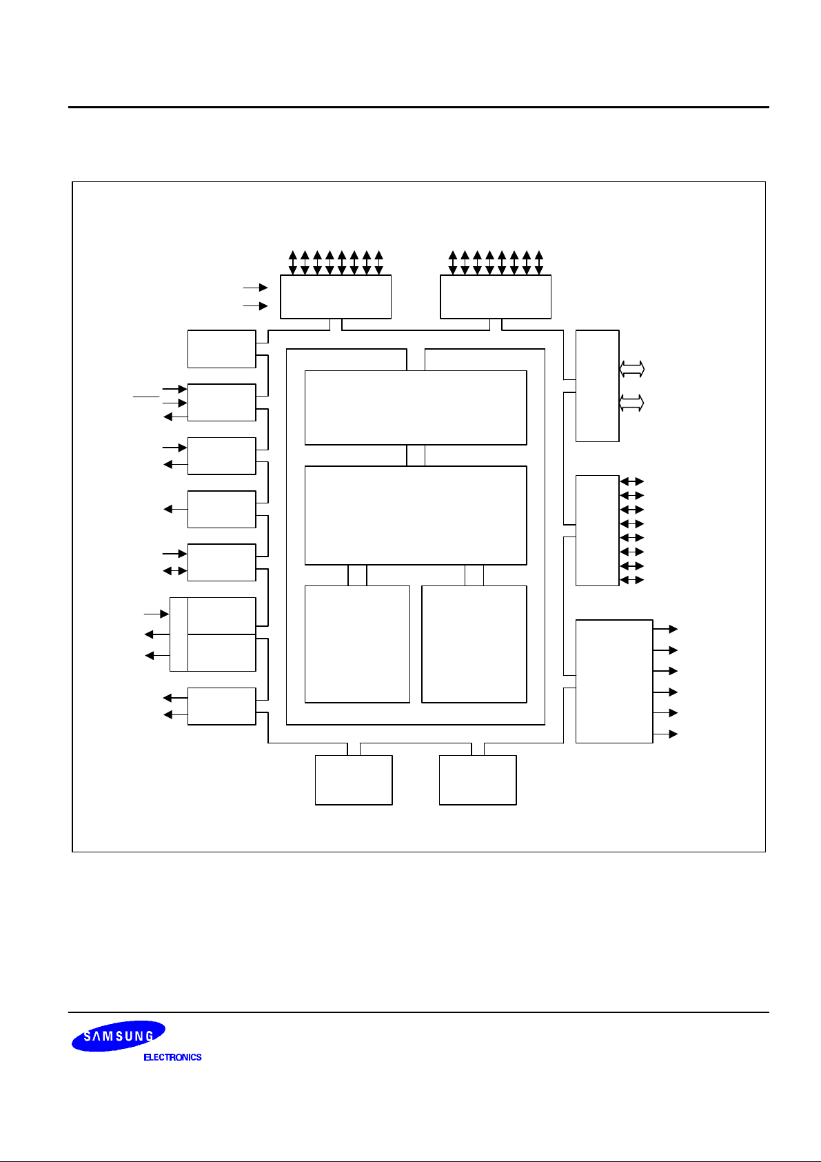
BLOCK DIAGRAM
RC/X-tal
XTOUT
P1.2/BUZ
P1.3/T0CK
P1.4/T0
P1.5/T1CK
P1.6/TA
P1.7/TB
PWM0
PWM1
OUT
X
XTIN
XIN
RESET
TEST
Watch
Timer 0
Timer 1
Timer A
Timer B
Module
Basic
Timer
Main
OSC
Sub
OSC
Timer
PWM
P4.0/SEG48-
P4.7/SEG55
Port 4 Port 3
Internal Bus
Port I/O and Interrupt
Control
SAM88RCRI CPU
64-Kbyte ROM
P3.0/SEG56-
P3.7/SEG63
592-Byte
Register File
Port 2
Port 1
LCD Driver/
Controller
P2.0/COM8P2.3/COM11
P2.4/COM12P2.7/COM15
P1.0/INT
P1.1/INT
P1.2/BUZ/INT
P1.3/T0CK/INT
P1.4/T0/INT
P1.5/T1CK/INT
P1.6/TA/INT
P1.7/TB/INT
VLC1
COM0-COM7
COM8/P2.0COM15/P2.7
SEG0-SEG47
SEG48/P4.0-
SEG55/P4.7
SEG56/P3.0SEG63/P3.7
Voltage
Level
Detector
192-Kbyte
Data
ROM
Figure 1-1. Block Diagram
1-3
PRODUCT OVERVIEW S3C921F/P921F
PIN ASSIGNMENTS
SEG21
SEG20
SEG19
SEG18
SEG17
SEG16
SEG15
SEG14
SEG13
SEG12
SEG11
SEG10
SEG9
SEG8
SEG7
SEG6
SEG5
SEG4
SEG3
SEG2
81
82
83
84
85
86
87
88
89
90
91
92
93
94
95
96
97
98
99
100
SEG1
SEG0
COM7
COM6
COM5
COM4
COM3
COM2
COM1
COM0
VLC1
RC/X-tal
PWM0
PWM1
VDD
VSS
XOUT
XIN
TEST
XTIN
XTOUT
RESET
P1.0/INT
P1.1/INT
P1.2/BUZ/INT
P1.3/T0CK/INT
P1.4/T0/INT
P1.5/T1CK/INT
P1.6/TA/INT
P1.7/TB/INT
1
2
3
4
5
6
7
8
9
10
11
12
13
14
15
16
17
18
19
20
21
22
23
24
25
26
27
28
29
30
31
(SDAT)
(SCLK)
33
32
34
S3C921F
(100-QFP-1420C)
39
38
37
36
35
40
41
42
43
44
45
46
47
48
49
50
80
79
78
77
76
75
74
73
72
71
70
69
68
67
66
65
64
63
62
61
60
59
58
57
56
55
54
53
52
51
SEG22
SEG23
SEG24
SEG25
SEG26
SEG27
SEG28
SEG29
SEG30
SEG31
SEG32
SEG33
SEG34
SEG35
SEG36
SEG37
SEG38
SEG39
SEG40
SEG41
SEG42
SEG43
SEG44
SEG45
SEG46
SEG47
P4.0/SEG48
P4.1/SEG49
P4.2/SEG50
P4.3/SEG51
1-4
P3.1/SEG57
P3.2/SEG58
P3.3/SEG59
P3.4/SEG60
P3.5/SEG61
P3.6/SEG62
P3.7/SEG63
P2.0/COM8
P2.1/COM9
P2.2/COM10
P2.3/COM11
P2.4/COM12
P2.5/COM13
P2.6/COM14
P2.7/COM15
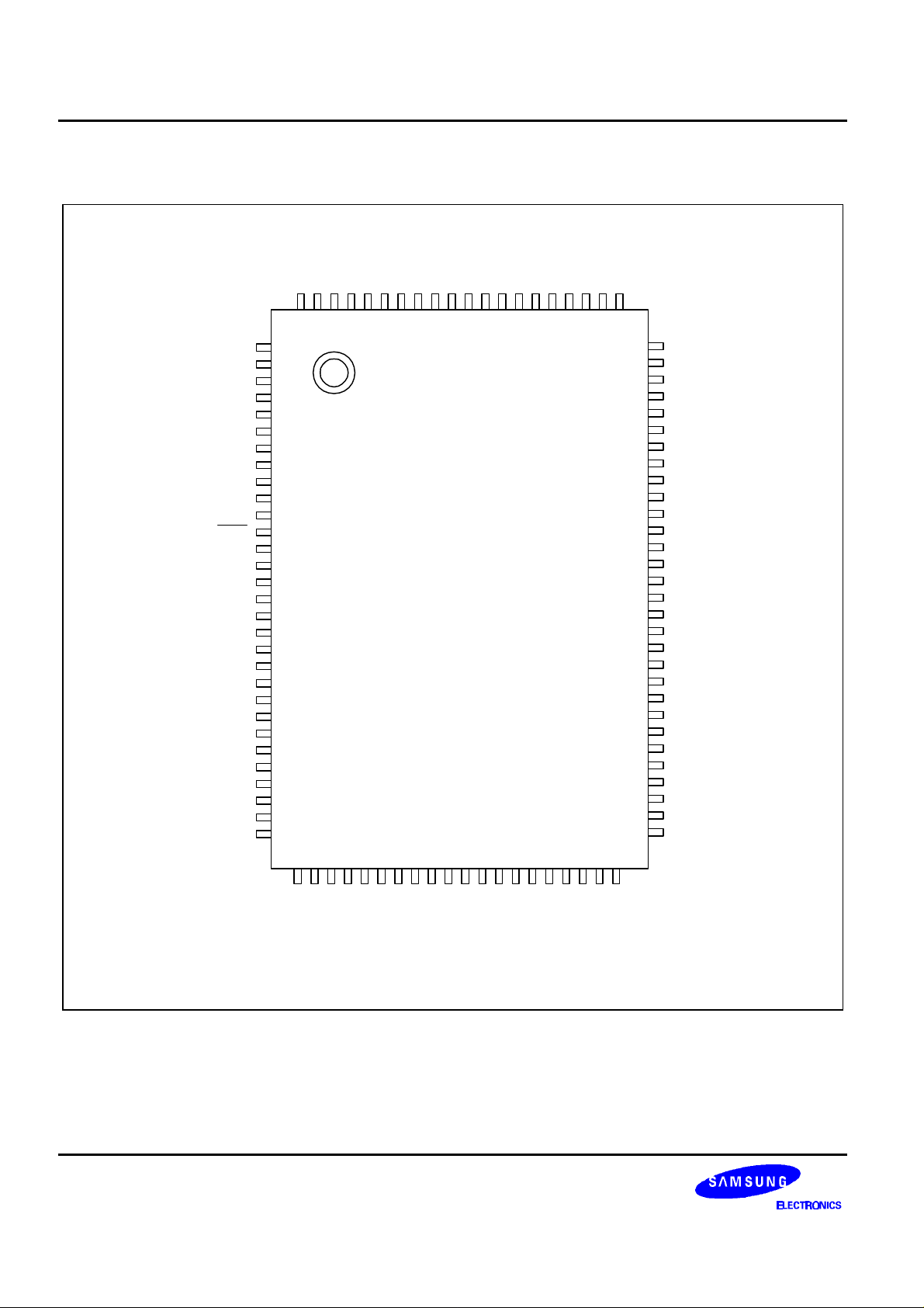
Figure 1-2. Pin Assignment (100 Pin)
P4.5/SEG53
P4.6/SEG54
P4.7/SEG55
P3.0/SEG56
P4.4/SEG52

S3C921F/P921F PRODUCT OVERVIEW
Table 1-1. Pin Descriptions
Pin Names Pin
P1.0, P1.1
P1.2
P1.3
P1.4
P1.5
P1.6
P1.7
P2.0 - P2.7
P3.0 - P3.7
P4.0 - P4.7
PWM0
PWM1
V
LC1
INT
BUZ
T0CK
T0
T1CK
TA
TB
COM0-COM7
COM8-COM15
SEG0-SEG47
SEG48-SEG55
SEG56-SEG63
Type
I/O
I/O
I/O
I/O
O
I
I/O
I/O
I/O
I/O
I/O
I/O
I/O
O
I/O
O
I/O
Pin Description Circuit
I/O port with bit-programmable pins;
Schmitt trigger input or push-pull, opendrain output and software assignable pullups;
Alternately used for external interrupt
input(noise filters, interrupt enable and
pending control).
I/O port with nibble-programmable pins;
Schmitt trigger input or push-pull, open-
Number
E-2 23, 24
H-9 38 - 31 COM8-
Pin
Numbers
25
26
27
28
29
30
Share
Pins
INT
BUZ/INT
T0CK/INT
T0/INT
T1CK/INT
TA/INT
TB/INT
COM15
drain output and software assignable pullups.
I/O port with bit-programmable pins;
Schmitt trigger input or push-pull, open-
H-8 46 - 39 SEG56-
SEG63
drain output and software assignable pullups.
I/O port with nibble-programmable pins;
Schmitt trigger input or push-pull output
H-10 54 - 47 SEG48-
SEG55
and software assignable pull-ups.
PWM output pins. C 13
–
14
LCD power supply pin. – 11 –
External interrupt input pins. E-2 23, 24
25
26
27
28
29
30
P1.0, P1.1
P1.2/BUZ
P1.3/T0CK
P1.4/T0
P1.5/T1CK
P1.6/TA
P1.7/TB
Output pin for buzzer signal. E-2 25 P1.2/INT
Timer 0 clock input. E-2 26 P1.3/INT
Capture input or interval/PWM output. E-2 27 P1.4/INT
Timer 1/A external clock input. E-2 28 P1.5
Timer 1/A clock output. E-2 29 P1.6
Timer B clock output. E-2 30 P1.7
LCD common data outputs. H-4 10 - 3 –
LCD common data outputs. H-9 38 - 31 P2.0 - P2.7
LCD segment data outputs. H-5 2-1
–
100-55
LCD segment data outputs. H-10
H-8
54 - 47
46 - 39
P4.0 - P4.7
P3.0 - P3.7
1-5
PRODUCT OVERVIEW S3C921F/P921F
Table 1-1. Pin Descriptions (Continued)
Pin Names Pin
Pin Description Circuit
Type
RESET
XTIN,XT
XIN,X
OUT
OUT
I System reset pin B 22 –
– Crystal oscillator pins for sub clock. – 20, 21
– Main oscillator pins. – 18, 17
RC/X-tal – Main oscillator type selection pin
("High" for RC osc. and "Low" for X-tal)
TEST I Test input: it must be connected to V
VDD,V
SS
– Power input pins – 15, 16
SS
Number
– 12
– 19
Pin
Numbers
Share
Pins
–
–
–
–
–
1-6

S3C921F/P921F PRODUCT OVERVIEW
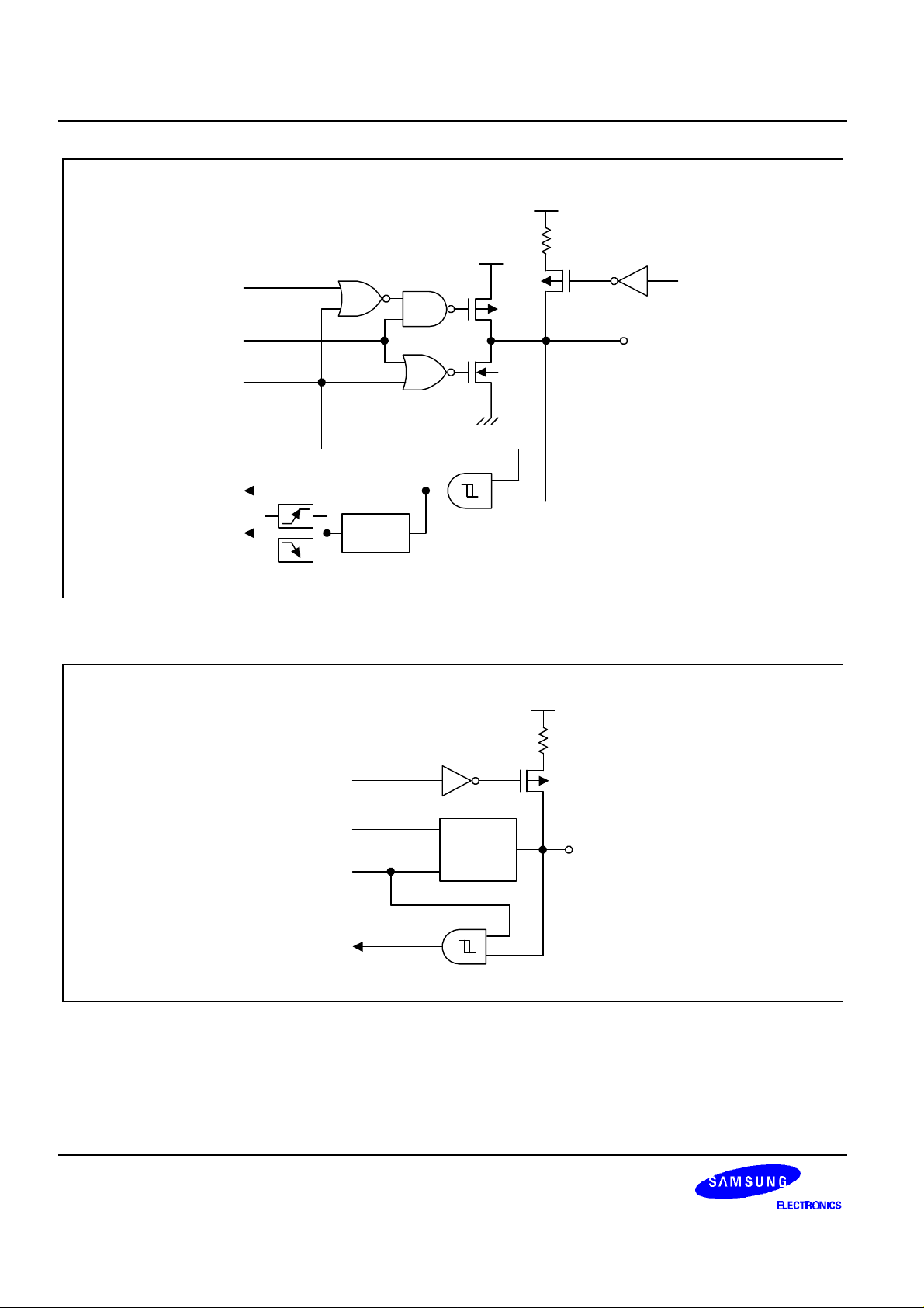
PIN CIRCUIT DIAGRAMS
VDD
P-Channel
In
N-Channel
Figure 1-3. Pin Circuit Type A
VDD
Pull-Up
Resistor
P-Channel
In
Pull-Up
Resistor
Enable
Data
Output
Disable
VDD
Pull-Up
Resistor
In
Schmitt Trigger
Figure 1-4. Pin Circuit Type B
VDD
P-Channel
Out
N-Channel
Schmitt Trigger
Figure 1-5. Pin Circuit Type A-3
Figure 1-6. Pin Circuit Type C
1-7
PRODUCT OVERVIEW S3C921F/P921F
VDD
Pull-up
VDD
Open-Drain
P-CH
Resistor
Resistor
Enable
Data
Output
Disable
External
Interrupt
Input
Noise
Filter
Figure 1-7. Pin Circuit Type E-2
Resistor
Enable
I/O
N-CH
VDD
Pull-up
Resistor
P-Channel
1-8
Data
Output
Disable
Circuit
Type C
Figure 1-8. Pin Circuit Type E-3
I/O
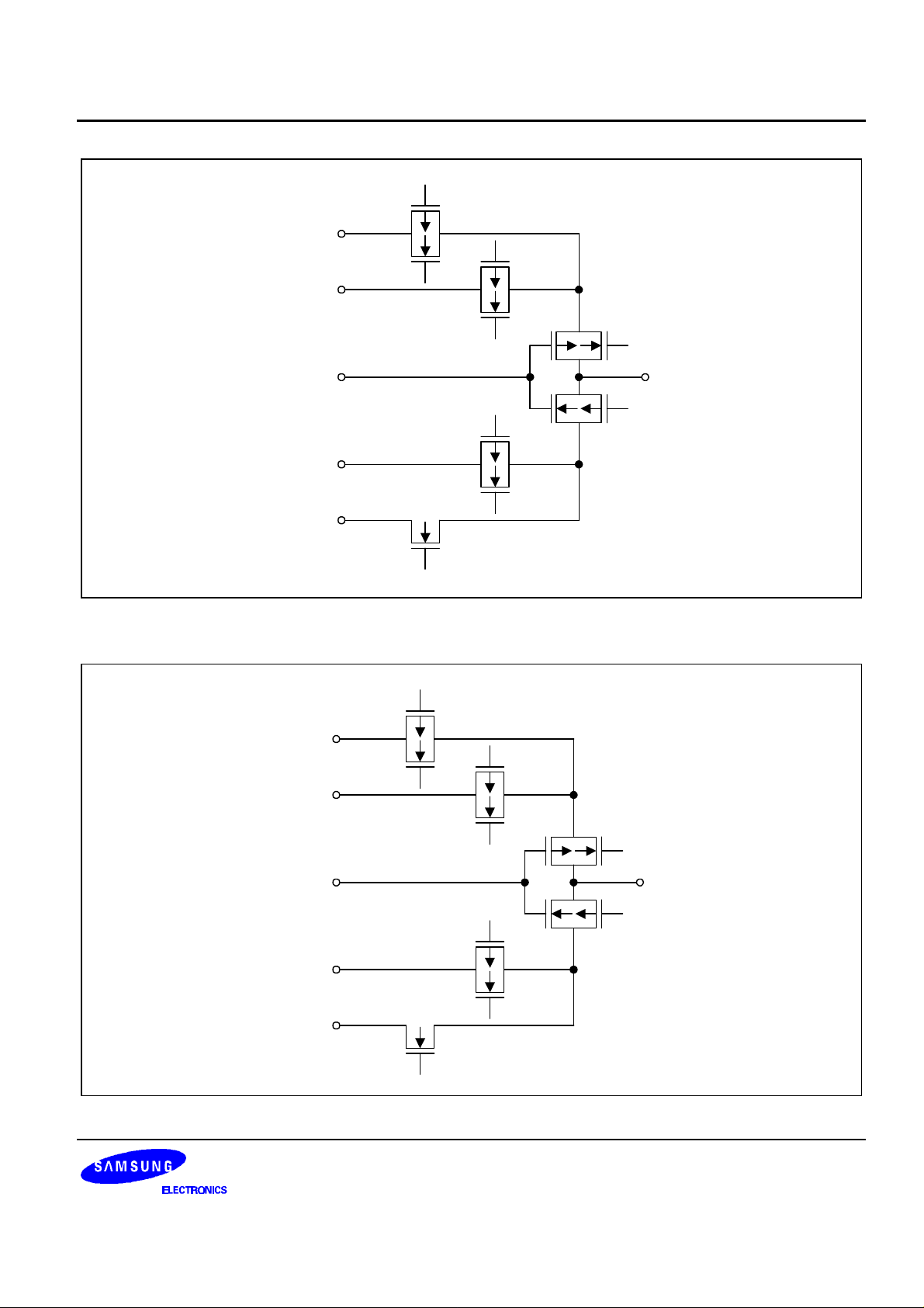
S3C921F/P921F PRODUCT OVERVIEW
VLC1
VLC2
COM Data
VLC5
VSS
VLC1
VLC3
Out
Figure 1-9. Pin Circuit Type H-4
SEG Data
VLC4
VSS
Out
Figure 1-10. Pin Circuit Type H-5
1-9
 Loading...