

Samsung S3C7031, S3C7032 Datasheet

S3C7031/7032 PRODUCT OVERVIEW
1 PRODUCT OVERVIEW
OVERVIEW
The S3C7031/7032 single-chip CMOS microcontroller has been designed for high performance using Samsung's
newest 4-bit CPU core.
With comparator inputs, high-current LED direct-drive pins, serial I/O interface, and a versatile 8-bit
timer/counter, the S3C7031/7032 offers an excellent design solution for a wide range of applications such as
mouse controllers, subsystem controllers, and toys.
Up to 15 pins of the 20-pin DIP or 20-pin SOP package can be dedicated to I/O. Pull-up resistors are assignable
to all of the pins by software. Four vectored interrupts provide fast response to internal and external events.
In addition, the S3C7031/7032's advanced CMOS technology provides for very low power consumption and a
wide operating voltage range.
DEVELOPMENT SUPPORT
The Samsung Microcontroller Development System, SMDS, provides you with a complete PC-based
development environment for KS57-series microcontrollers that is powerful, reliable, and portable. In addition to
its easy to use window-oriented program development structure, the SMDS toolset includes versatile debugging,
trace, instruction timing, and performance measurement applications.
The Samsung Generalized Assembler (SAMA) has been designed specifically for the SMDS environment and
accepts assembly language sources in a variety of microprocessor formats.
SAMA generates industry-standard object files that also contain program control data for SMDS compatibility.
1-1

PRODUCT OVERVIEW S3C7031/7032
FEATURES
Memory
— 1024 × 8-bit program memory (S3C7031)
(ROM)
— 2048 × 8-bit program memory (S3C7032)
(ROM)
— 128 × 4-bit data memory (S3C7031) (RAM)
— 256 × 4-bit data memory (S3C7032) (RAM)
I/O Pins
— Up to 15 pins for 20-DIP and 20-SOP package
Comparator Inputs
— 4-channel mode
Internal reference: 4-bit resolution
— 3-channel mode
External reference
8-Bit Basic Timer
— Programmable interval timer
8-Bit Serial I/O Interface
— 8-bit transmit/receive mode
— 8-bit receive-only mode
— LSB-first or MSB-first transmission selectable
— Internal or external clock source
Interrupts
— One external interrupt vector
— Three internal interrupt vectors
— Two quasi-interrupts
Memory-Mapped I/O Structure
Two Power-Down Modes
— Idle mode: Only the CPU clock stops
— Stop mode: Main system clock stops
On-Chip Crystal, Ceramic, Or RC Oscillator
— Crystal/ceramic: 4.19 MHz (typical)
— RC: 1 MHz (typical)
— CPU clock divider circuit (by 4, 8, or 64)
8-Bit Timer/Counter
— Programmable interval timer
— External event counter function
— Timer clock output to TIO pin
Watch Timer
— Time interval generation: 0.5 s, 3.9 ms at
4.19 MHz
— Four frequency outputs to BUZ pin
Bit Sequential Carrier
— 16-bit serial data transfer in arbitrary format
Frequency Outputs
— Eight frequency outputs to the CLO pin
Instruction Execution Times
— 0.95, 1.91, 15.3 µs at 4.19 MHz (5 V),
4 µs at 1 MHz (2.7 V)
Operating Temperature:
— – 40°C to 85°C
Operating Voltage Range:
— 2.7 V to 6.0 V
Package Type:
— 20-DIP, 20-SOP
1-2

S3C7031/7032 PRODUCT OVERVIEW
BLOCK DIAGRAM
X
RESET
X
OUT
IN
P2.0 - P2.3
P3.0/SCK
P3.1/SO
P3.2/SI
P3.3/BUZ
Basic
Timer
Watch
Timer
I/O Port 2
I/O Port 3
Serial I/O Port
Interrupt
Control
Block
Internal
Interrupts
Instruction Decoder
Arithmetic
Logic Unit
Data
Memory
NOTES:
1. Program Memory is 1-KByte (S3C7031) and 2-KByte (S3C7032).
2. Data Memory is 128 x 4bit (S3C7031) and 256 x 4bit (S3C7032).
(2)
Clock
and
Stack
Pointer
Program
Counter
Program
Status Word
Flags
Program
Memory
(1)
I/O Port 0
8-Bit
Timer/
Counter
Comparator
I/O Port 1
P0.0/CLO
P0.1/TIO
P0.2/INT1
P0.0/KS0/CIN0
P0.1/KS1/CIN1
P0.2/KS2/CIN2
P0.3/KS3/CIN3
Figure 1-1. S3C7031/7032 Block Diagram
1-3
PRODUCT OVERVIEW S3C7031/7032
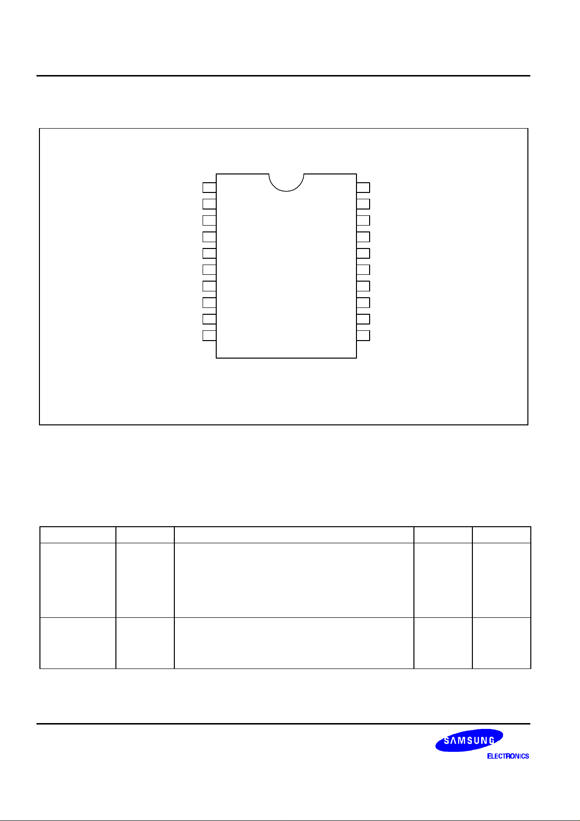
PIN ASSIGNMENTS
P0.0/CLO
P0.1/TIO
P0.2/INT1
P0.0/KS0/CIN0
P0.1/KS1/CIN1
P0.2/KS2/CIN2
P0.3/KS3/CIN3
XOUT
XIN
VSS
NOTE: Pin assignments are identical for the 20-pin DIP and SOP package.
1
2
3
4
5
6
7
8
9
10
KS57C7031/
KS57C7032
(Top view)
20
19
18
17
16
15
14
13
12
11
VDD
P3.3/BUZ
P3.2/SI
P3.1/SO
P3.0/SCK
P2.3
P2.2
P2.1
P2.0
RESET
Figure 1-2. S3C7031/7032 Pin Assignment Diagram (20-pin DIP/SOP Package)
PIN DESCRIPTIONS
Table 1-1. S3C7031/7032 Pin Descriptions
Pin Name Pin Type Description Number Share Pin
P0.0
P0.1
P0.2
P1.0
P1.1
P1.2
P1.3
1-4
I/O 3-bit I/O port.
1-bit or 3-bit read/write and test is possible.
Pull-up resistors are individually assignable to input
pins by software and are automatically disabled for
output pins.
Pins are individually configurable as input or output.
I/O Same as port 0 except that port 1 is a 4-bit I/O port. 4
1
2
3
KS0/CIN0
5
6
7
KS1/CIN1
KS2/CIN2
KS3/CIN3
CLO
TIO
INT1
S3C7031/7032 PRODUCT OVERVIEW
Table 1-1. S3C7031/7032 Pin Descriptions (Continued)
Pin Name Pin Type Description Number Share Pin
P2.0-P2.3
P3.0
P3.1
P3.2
P3.3
I/O 4-bit I/O port. 1-bit, 4-bit or 8-bit read/write and test is
possible. Pins are individually configurable as input
or output.
Pull-up resistors are individually assignable to input
pins by software and are automatically disabled for
12-15
16
17
18
19
–-
SCK
SO
SI
BUZ
output pins. Ports are software configurable as
n-channel open-drain outputs or push-pull output by
software.
Ports 2 and 3 can be paired to enable 8-bit data
transfer.
CLO I/O Eight frequency outputs 1 P0.0
TIO I/O External clock input or timer clock output 2 P0.1
INT1 I/O External interrupts with rising or falling edge
3 P0.2
detection
KS0-KS3 I/O Quasi-interrupts with falling edge detection 4-7 P1.0-P1.3
CIN0-CIN3 I/O 4-channel comparator input.
4-7 P1.0-P1.3
CIN0-CIN2: comparator input only.
CIN3: comparator input or external reference input
SCK
I/O Serial interface clock signal 16 P3.0
SO I/O Serial data output 17 P3.1
SI I/O Serial data input 18 P3.2
BUZ I/O 2 kHz, 4 kHz, 8 kHz, or 16 kHz frequency output at
19 P3.3
4.19 MHz for buzzer sound
XIN, X
RESET
V
DD
V
SS
OUT
–- Crystal, ceramic, or RC signal for system clock 9, 8 –-
I Reset signal 11 ––- Power supply 20 ––- Ground 10 –-
Table 1-2. Overview of S3C7031/7032 Pin Data
Pin Numbers Pin Names Share Pins I/O Type Reset Value Circuit Type
1-3 P0.0-P0.2 CLO, TIO, INT1 I/O Input 2
4-7 P1.0-P1.3 KS0/CIN0-KS3/CIN3 I/O Input 4
12-5 P2.0-P2.3 – I/O Input 3
16-19 P3.0-P3.3
11
20, 10
9, 8
RESET
VDD, V
XIN, X
SS
OUT
SCK, SO, SI, BUZ
–- I –- 1
–- –- –- ––- –- –- –-
I/O Input 3
1-5
PRODUCT OVERVIEW S3C7031/7032
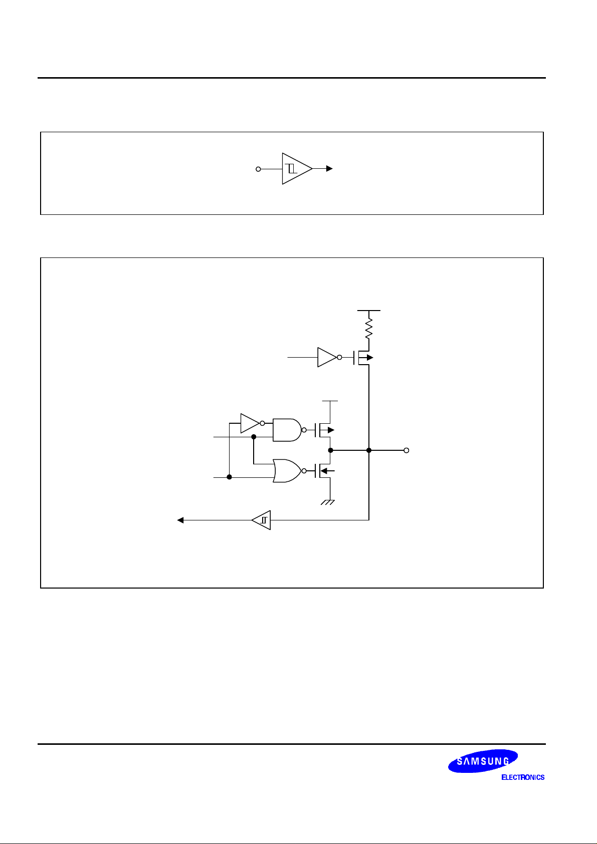
PIN CIRCUIT DIAGRAMS
In
Schmitt Trigger
Figure 1-3. Pin Circuit Type 1
VDD
Data
Output DIsable
Pull-up
Registor
Pull-up Enable
VDD
VSS
Schmit Trigger
Figure 1-4. Pin Circuit Type 2
Typical 50 KΩ
(VDD = 5V)
I/O
1-6
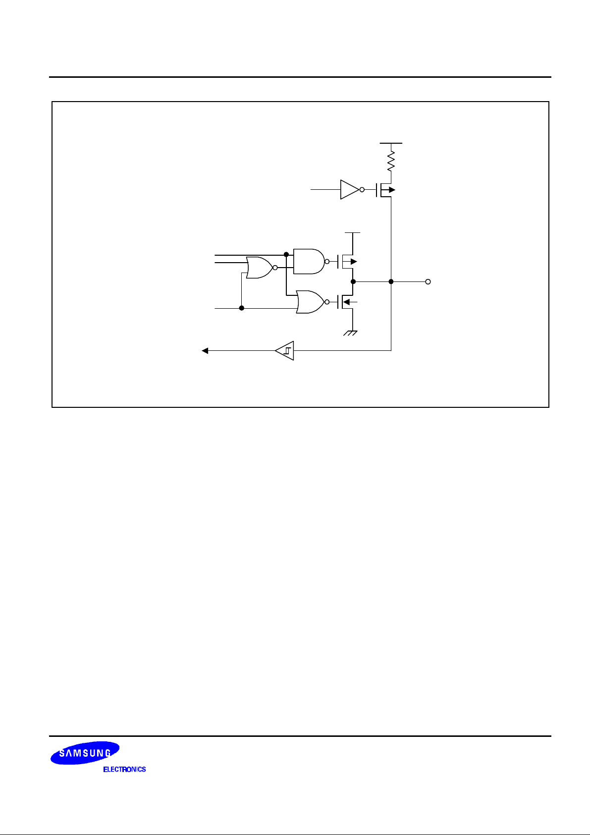
S3C7031/7032 PRODUCT OVERVIEW
VDD
Data
Open-drain
Output Disable
Pull-up
Registor
Pull-up Enable
VDD
Schmit Trigger
Figure 1-5. Pin Circuit Type 3
Typical 50 KΩ
(VDD =5V)
I/O
VSS
1-7
PRODUCT OVERVIEW S3C7031/7032
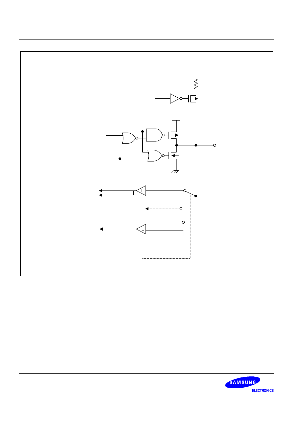
VDD
Output Disable
(Digital)
Data
Open-drain
In
Intk
(Quasi)
In
Pull-up Enable
Schmit Trigger
REF
(P1.3 Only)
+
Pull-up
Registor
VDD
VSS
Typical 50 KΩ
(VDD =5V)
P-CH
I/O
(Analog) Comparator
Digital or Analog
Selectable by Software
Figure 1-6. Pin Circuit Type 4
REF
1-8
 Loading...