

Page 1
Approval
TO
DATE
SAMSUNG TFT-LCD
SAMSUNG TFT-LCD
MODEL NO.:LTN154AT13-L02
MODEL NO.:LTN154AT13-L02
NOTE : Surface type [ Anti Glare ]
: Lenovo
: Sep. 12th, 2008
Green product (Complied with RoHS requirement)
APPROVED BY :
PREPARED BY : Mobile Division, Application Engineering Part
SAMSUNG ELECTRONICS CO., LTD.
SEC Secret
Doc.No. Rev.No Page / 30LTN154AT13-L02 1
04-A03-S-080912
Page 2
CONTENTS
Approval
Revision History
General Description
1. Absolute Maximum Ratings
1.1 Absolute Ratings of environment
1.2 Electrical Absolute Ratings
2. Optical Characteristics
3. Electrical Characteristics
3.1 TFT LCD Module
3.2 Backlight Unit
4. Block Diagram
4.1 TFT LCD Module
4.2 Backlight Unit
5. Input Terminal Pin Assignment
5.1 Input Signal & Power
5.2 LVDS Interface
5.3 Backlight Unit
5.4 Timing Diagrams of LVDS For Transmitting
5.5 Input Signals, Basic Display Colors and Gray Scale of Each Color.
5.6 Pixel format
- - - - - - - - - - - - - - - - - - - ( 3 )
- - - - - - - - - - - - - - - - - - - ( 5 )
- - - - - - - - - - - - - - - - - - - ( 6 )
- - - - - - - - - - - - - - - - - - - ( 8 )
- - - - - - - - - - - - - - - - - - - ( 12 )
- - - - - - - - - - - - - - - - - - - ( 15 )
- - - - - - - - - - - - - - - - - - - ( 16 )
6. Interface Timing
6.1 Timing Parameters(DE Mode)
6.2 Timing Diagrams of interface Signal (DE Mode)
6.3 Power ON/OFF Sequence
7. Outline Dimension
8. Product Markings and Others
9. General Precautions
10. EDID
- - - - - - - - - - - - - - - - - - - ( 21 )
- - - - - - - - - - - - - - - - - - - ( 23 )
- - - - - - - - - - - - - - - - - - - ( 25 )
- - - - - - - - - - - - - - - - - - - ( 26 )
- - - - - - - - - - - - - - - - - - - ( 28 )
SEC Secret
Doc.No. Rev.No Page / 30LTN154AT13-L02 2
04-A03-S-080912
Page 3
REVISION HISTORY
REVISION HISTORY
Approval
SummaryPageRevision No.Date
AllP00Aug. 26, 2006
AllA00Aug. 28, 2008
- LTN154AT13-L02 model specification was First issued.
SEC’s P/N
LTN154AT13-L02
Lenovo’s product code
Lenovo P/N : 42T0588
FRU P/N : 42T0589
EC NO : Header Code : 1ZF0P
-LTN154AT13-L02 approval specification was issued first.
SEC’s P/N
LTN154AT13-L02
Lenovo’s product code
Lenovo P/N : 42T0588
FRU P/N : 42T0589
EC NO : Header Code : 1ZF0P
- Backlight unit (FPC) was updated.p. 17A01Aug. 29. 2008
- Backlight unit (FPC) was updated.p. 17A02Sep. 3. 2008
A03Sep.11.2008
p. 13
p. 6,13
-Backlight unit (life time) was updated.
- LED forward current spec was updated.
SEC Secret
Doc.No. Rev.No Page / 30LTN154AT13-L02 3
04-A03-S-080912
Page 4
Approval
GENERAL DESCRIPTION
DESCRIPTION
LTN154AT13-L02 is a color active matrix TFT (Thin Film Transistor) liquid crystal display
(LCD) that uses amorphous silicon TFT as a switching devices. This model is composed of
a TFT LCD panel, a driver circuit and a backlight system. The resolution of a 15.4" contains
1,280 x 800 pixels and can display up to 262,144 colors. 6 O'clock direction is the Optimum
viewing angle.
FEATURES
• Thin and light weight
• High contrast ratio, high aperture structure
• Wide XGA (1280x800 pixels) resolution
• Fast Response Time
• Low power consumption
• LED Back Light
• DE (Data enable) only mode.
• 3.3V LVDS Interface
• On board EDID chip
• Auto Recovery Function
• RoHS Compliance
APPLICATIONS
• Notebook PC and desktop monitors
•If the usage of this product is not for PC application, but for others, please contact SEC
GENERAL INFORMATION
mm
pixel
mm
Pixel pitch
331.2(H) X 207.0(V) (15.4”diagonal)Display area
a-si TFT active matrixDriver element
262,144Display colors
1280 x 800 ( 16 : 10, Wide XGA )Number of pixel
RGB vertical stripePixel arrangement
0.25875(H) x 0.25875(V)
NoteUnitSpecificationItem
Normally whiteDisplay Mode
HAZE 25, HARD-COATING 3H, AGSurface treatment
SEC Secret
Doc.No. Rev.No Page / 30LTN154AT13-L02 4
04-A03-S-080912
Page 5
Mechanical Information
Approval
Module
size
1. ABSOLUTE MAXIMUM RATINGS
1.1 ENVIRONMENTAL ABSOLUTE RATINGS
Storage temperate
Operating temperate
(Temperature of glass surface)
STG
OPR
Max.
344.5
222.6
6.5
560
NoteUnitTyp.Min.Item
mm344.0343.5Horizontal (H)
mm222.1221.6Vertical (V)
mm6.2-Depth (D)
g530-Weight
NoteUnitMax.Min.SymbolItem
(1)°C60-20 T
(1)°C500T
-SnopShock ( non-operating )
Note (1) Temperature and relative humidity range are shown in the figure below.
95 % RH Max. ( 40 OC ≥ Ta)
Maximum wet - bulb temperature at 39 OC or less. (Ta > 40 OC) No condensation.
(2) 3ms, half sine wave, one time for ±X,±Y,±Z.
(3) 18ms, Trapezoidal wave, one time for ±X,±Y,±Z.
(4) 5~500 Hz, Random vibration, 30 min for X,Y,Z.
(5) At testing Vibration and Shock, the fixture in holding the Module to be tested have to be
hard and rigid enough so that the Module would not be twisted or bent by the fixture.
100
-40 -20 0 20 40 60 80
Relative Humidity ( %RH)
95
80
60
40
20
Operating Range
8
Storage Range
5
0
Temperature (
O
C)
210
G
(2),(5)
(3),(5)50
(4),(5)G2.41-VnopVibration (non-operating)
SEC Secret
Doc.No. Rev.No Page / 30LTN154AT13-L02 5
04-A03-S-080912
Page 6
1.2 ELECTRICAL ABSOLUTE RATINGS
Approval
(1) TFT LCD MODULE
Power Supply Voltage
Logic Input Voltage
NOTE (1) Within Ta ( 25 ± 2 OC )
DD
IN
VDD=3.3V, V
(2) BACK-LIGHT UNIT
Min
LED Current
LED Voltage
NOTE (1) Permanent damage to the device may occur if maximum values are exceeded.
Functional operation should be restricted to the conditions described under Normal Operating
Conditions.
L
V
-
-
SS
= GND = 0V
NoteUnitMax.Min.SymbolItem
(1)VVDD+ 0.3VDD- 0.3V
(1)VVDD+ 0.3VDD- 0.3V
Ta = 25 ± 2 °C
NoteUnitMax.Typ.SymbolItem
(1)mA1918I
(1)V-3.2F
SEC Secret
Doc.No. Rev.No Page / 30LTN154AT13-L02 6
04-A03-S-080912
Page 7
Approval
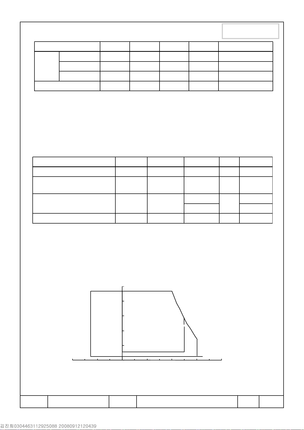
2. OPTICAL CHARACTERISTICS
The following items are measured under stable conditions. The optical characteristics
should be measured in a dark room or equivalent state with the methods shown in Note (5).
Measuring equipment : TOPCON SR-3
Contrast Ratio
(5 Points)
Response
Time at 25℃
Average Luminance
of White (5 points)
Color
Chromaticity
( CIE )
Rising
Falling
Red
Green
Blue
* Ta = 25±2oC , Vcc=3.3V, fv= 60Hz, f
CR
f
AVE
Normal
X
Viewing
0.555R
0.585
Angle
Y
X
Y
X
Y
φ = 0
θ = 0
0.311R
0.312G
0.532G
0.121B
0.083B
0.341
0.342
0.562
0.151
0.113
DCLK
=71.11MHz, IL= 18mArms
Unit
-
2516TR+T
2
-200175YL,
cd/m
0.615
0.371
0.372
0.592
-
0.181
0.143
NoteMaxTyp.Min.ConditionSymbolItem
(1), (2), (5)-500300
(1), (3)msec-
IL=18mA
(1), (4)
(1), (5)
SR-3
Viewing
Angle
13 Points
White Variation
5 Points
White Variation
SEC Secret
White
Hor.
Ver.
X
Y
θ
L
H
CR ≥ 10
H
L
L
L
0.3430.3130.283W
0.3590.3290.299W
-45-
-45-θ
-20-φ
Degree
s
(1), (5)
SR-3
-45-φ
(6)%--60%δ
%
(6)--80%δ
Doc.No. Rev.No Page / 30LTN154AT13-L02 7
04-A03-S-080912
Page 8
Approval
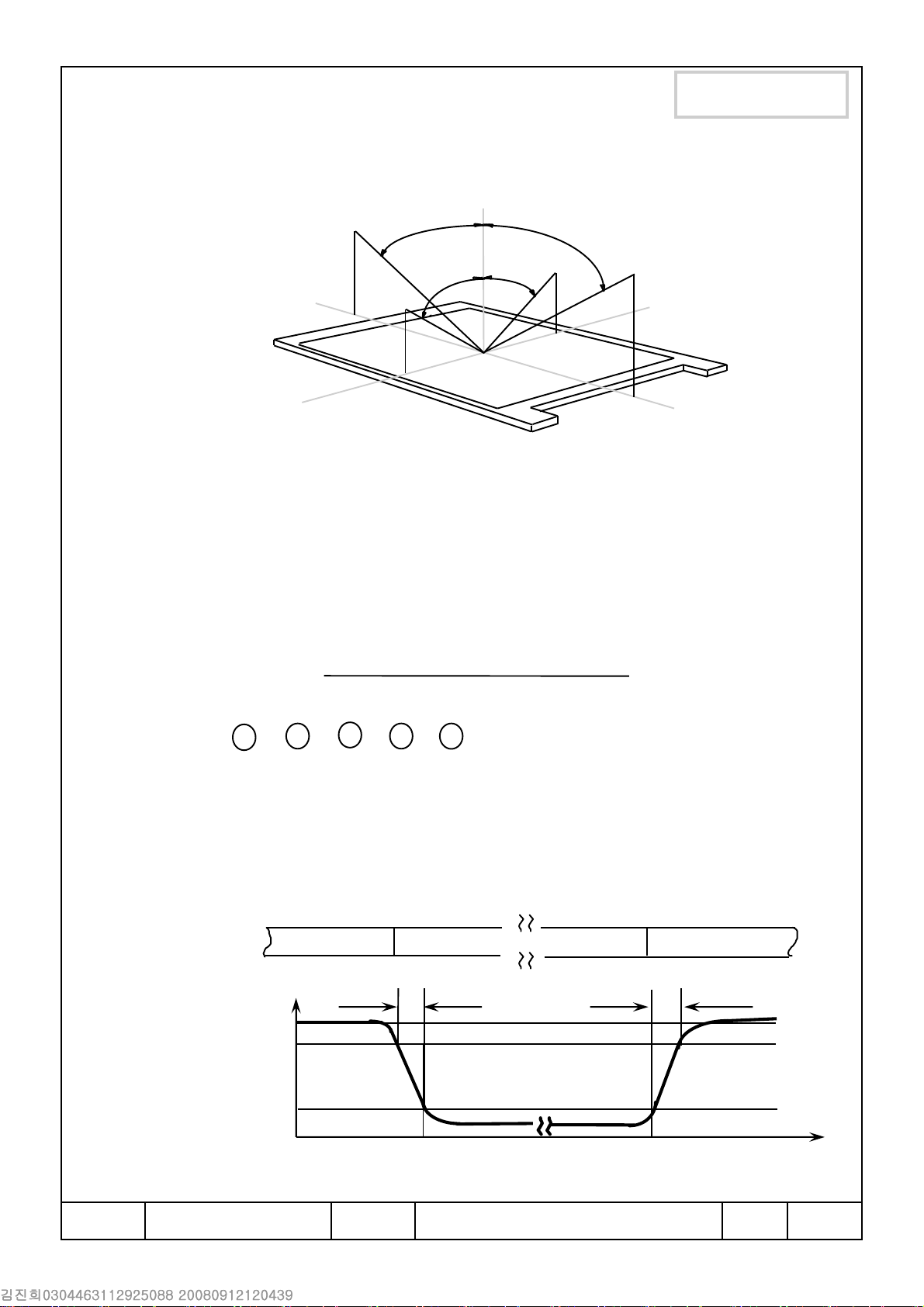
Note 1) Definition of Viewing Angle : Viewing angle range (10
Normal Line
o
,
θ = 0
o
θL =90
φ = 0
θ
L
φ
φ
o
x
L
H
6 o'clock
direction
o
φL= 90
≤≤≤≤
C/R at center point )
θ
R
y
x'y'
12 o'clock
direction
φH= 90
θR=90
o
o
Note 2) Definition of Contrast Ratio (CR) : Ratio of gray max (Gmax) ,gray min (Gmin)
at 5 points(4, 5, 7, 9, 10)
CR(4) + CR(5) + CR(7) + CR(9) + CR(10)
CR =
5
POINTS : , 5 , , , at FIGURE OF NOTE 6)
Note 3) Definition of Response time :Note 3) Definition of Response time : Sum of TR ,T
Display data
Optical
Response
4 9
White(TFT OFF) White(TFT OFF)
7
10
F
Black(TFT ON)
T
R
T
F
100%
90%
10%
0%
Time
SEC Secret
Doc.No. Rev.No Page / 30LTN154AT13-L02 8
04-A03-S-080912
Page 9
Approval
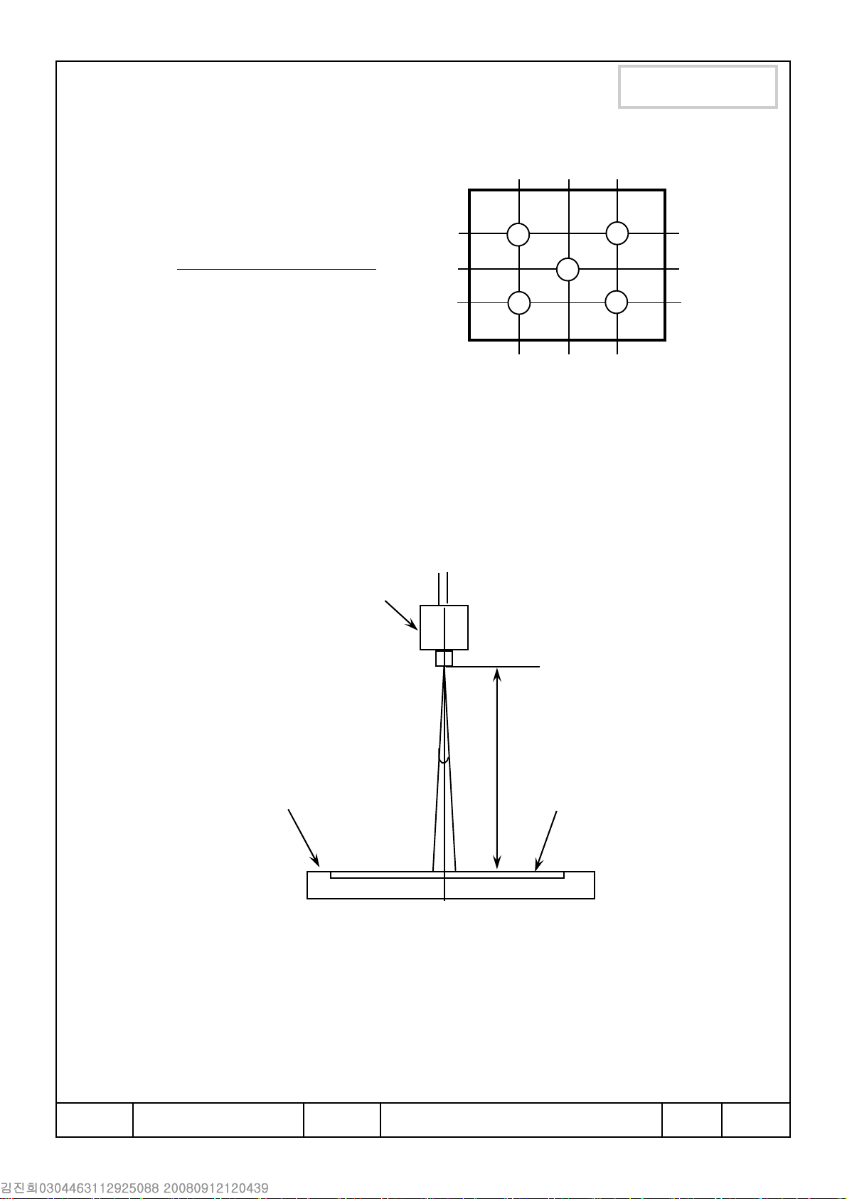
Note 4) Definition of Luminance of White : measure the luminance of white at 5 points.
(960)
VIEW AREA
9
7
(200)
(400)
Average Luminance of White ( Y
YL4+ YL5+ YL7+ YL9+ Y
Y
L,AVE
=
L,AVE
(320) (640)
)
10
L10
5
5
4
(600)
(lines)
Note 5) After stabilizing and leaving the panel alone at a given temperature for 30 min , the measurement
should be executed. Measurement should be executed in a stable, windless,and dark room.
30 min after lighting the back-light. This should be measured in the center of screen.
Lamp current : 6.0mArms
Environment condition : Ta = 25oC ±2 oC
TFT-LCD module
Photo-detector
( TOPCON SR-3)
Field = 2
o
SR-7 : 50 cm
LCD panel
center of the screen
Optical characteristics measurement setup
SEC Secret
Doc.No. Rev.No Page / 30LTN154AT13-L02 9
04-A03-S-080912
Page 10

Approval
Note 6) Definition of 13 points white variation, CR variation( C
13 points
white variation
Meet ISO13406-2 Luminance uniformity
10mm
10mm
13 12
8
Minimum luminance of 13 points
=
Maximum luminance of 13 points
320 640 960
10
7
VER
) [ ~ ]
X 100(%)
10mm
11
9
6
1 13
VIEW AREA
200
400
: test point
5
10mm
Note 7) Definition of 5 points white variation, CR variation( C
5 points
white variation
3
Minimum luminance of 5 points
=
Maximum luminance of 5 points
2
4
1
VER
) [ 4,5,7,9,10 ]
600
X 100(%)
SEC Secret
Doc.No. Rev.No Page / 30LTN154AT13-L02 10
04-A03-S-080912
Page 11

3. ELECTRICAL CHARACTERISTICS
Approval
3.1 TFT LCD MODULE
ITEM SYMBOL MIN TYP MAX UNIT NOTE
Voltage of Power Supply V
Differential Input
Voltage for LVDS
Receiver Threshold
Vsync
60Hz
F
r
e
q
50Hz
u
e
n
c
40Hz
y
Rush Current I
High
Low
Main Freq
Hsync Freq
Main Freq
Hsync Freq
Main Freq
White
F
F
F
DD
V
IH
V
IL
F
H
DCLK
F
H
DCLK
F
H
DCLK
RUSH
Ta=25 ± 2 ºC
3.0 3.3 3.6 V
- - +100 mV
VCM=+1.2V
-100 - - mV
48.24 60
65.12 85
40.2
54.27
32.16
43.41
49.38
71.11
41.15 KHz
59.26
32.92
47.4
50
70.83
40
56.67
KHzHsync Freq
MHz
MHz
KHz
MHz
- - 1.5 A (4)
- 300 - mA (2),(3)*a
I
Mosaic (2),(3)*b
DD
- 350 - mA
Current of
Power Supply
WinXP
Pattern
Max
Pattern
-
-
350
450
520
Note (1) Display data pins and timing signal pins should be connected.(GND=0V)
(2) fV=60Hz, f
DCLK
=71.11MHZ, Vdd = 3.3V , DC Current.
(3) Power dissipation pattern
*a) White Pattern *b) Mosaic Pattern
VIEW AREA
Display Brightest Gray Level
Display Darkest Gray Level
mA
mA
(2),(3)*c-
(2),(3)*d
SEC Secret
Doc.No. Rev.No Page / 30LTN154AT13-L02 11
04-A03-S-080912
Page 12

*c) WinXP Pattern
*d) 1dot Inversion Pattern
Approval
4) Rush current measurement condition
3.3V
R1
47K
CONTROL SIGNAL
(HIGH to LOW)
12V
R2
1K
R3
C2
M1
2SK1059
M2
2SK1399
FUSE
RGB
R B
G
G
R
G
R B
C1
1uF
R GB R
B
R B
G
R GB R
R B
G
V
DD (
LCD INPUT)
G
G
C3
1uF
47K
10000pF
VDDrising time is 470us
3.3V
GND
0.1V
DD
0.9V
DD
470us
SEC Secret
Doc.No. Rev.No Page / 30LTN154AT13-L02 12
04-A03-S-080912
Page 13

3.2 BACK-LIGHT UNIT
Approval
White LED chip P/N : SLSNNWH421US (SEM)
LED Forward Current
LED Forward Voltage
LED Array Voltage
Note (1) Life time (Hr) of LEDs can be defined as the time in which it continues to operate under the
condition Ta= 25 ± 2 °C and IF= 18.0 mA until one of the followingevent occurs.
- When the brightness becomes 50% or lower than the original
- LCD module MTBF
F
F
P
mA1918-I
V-3.2-V
W-2.76-PPower Consumption
Ta= 25 ± 2 °C
NoteUnitMax.Typ.Min.SymbolItem
VFX 8 LEDsV-25.6-V
IFX VFX 48LEDs
6 parallel, 8 serial
(1)Hr-10,000-HrOperating Life Time
Ta= 25 ± 2 °C
SEC Secret
Doc.No. Rev.No Page / 30LTN154AT13-L02 13
04-A03-S-080912
Page 14

4. BLOCK DIAGRAM
4.1 TFT LCD Module
Approval
Input Connector
Video Signal
Control Signal
VCOM
Gamma
DVDD
AVDD
Von/Voff
LVDS
LVDS Input/RSDS Output
DC-DC
Converter
Timing Controller
Gamma
Generator
VCOM
Generator
SOURCE PCB
RSDS
Source
Driver
IC
Gate Driver IC Integrated
15.4” WXGA
TFT-LCD Panel
SEC Secret
Doc.No. Rev.No Page / 30LTN154AT13-L02 14
04-A03-S-080912
Page 15

5. INPUT TERMINAL PIN ASSIGNMENT
5.1. Input Signal & Power (LVDS Connector : IS100-L30R-C15, UJU )
POWER SUPPLY, +3.3VVDD2222
POWER SUPPLY, +3.3VVDD3333
FunctionSymbol
FunctionFunction
GROUNDGND1111
Pin No.
Pin No.Pin No.
SymbolPin No.
SymbolSymbol
Approval
Remark
RemarkFunction
RemarkRemark
10
1010
11
1111
12
1212
13
1313
14
1414
15
1515
16
1616
17
1717
4444
6666
7777
V
CLK
DATA
EDID
EDID
EDID
Negative LVDS Differential Data Input For Odd PixelORX0-8888
Positive LVDS Differential Data Input For Odd PixelORX0+9999
Negative LVDS Differential Data Input For Odd PixelORX1-11
Positive LVDS Differential Data Input For Odd PixelORX1+12
Negative LVDS Differential Data Input For Odd PixelORX2-14
Positive LVDS Differential Data Input For Odd PixelORX2+15
Negative LVDS Differential Clock Input For Odd PixelORXC-17
DDC +3.3V POWER
BIST Mode Control PinBIST_CON5555
DDC CLOCK
DDC DATA
GROUNDGND10
GROUNDGND13
GROUNDGND16
18
1818
19
1919
20
2020
21
2121
22
2222
23
2323
24
2424
25
2525
26
2626
27
2727
28
2828
29
2929
30
3030
Positive LVDS Differential Clock Input For Odd PixelORXC+18
GROUNDGND19
NCERX0-20
NCERX0+21
NCGND22
NCERX1-23
NCERX1+24
NCGND25
NCERX2-26
NCERX2+27
NCGND28
NCERXC-29
NCERXC+30
SEC Secret
Doc.No. Rev.No Page / 30LTN154AT13-L02 15
04-A03-S-080912
Page 16

5.2 LVDS Transmitter : Transmitter DS90CF383 or Compatible
Pin No. Name RGB Signal Pin No. Name RGB Signal
51 TxIN0 R0 14 TxIN14 G5
52 TxIN1 R1 15 TxIN15 B0
54 TxIN2 R2 19 TxIN18 B1
55 TxIN3 R3 20 TxIN19 B2
56 TxIN4 R4 22 TxIN20 B3
3 TxIN6 R5 23 TxIN21 B4
4 TxIN7 G0 24 TxIN22 B5
6 TxIN8 G1 27 TxIN24 Hsync
7 TxIN9 G2 28 TxIN25 Vsync
Approval
11 TxIN12 G3 30 TxIN26 DE
12 TxIN13 G4 31 TxCLKIN Clock
FLAT LINK INTERFACE
Graphics controller
18-bit
RED0
RED1
RED2
RED3
RED4
RED5
GREEN0
GREEN1
GREEN2
GREEN3
GREEN4
GREEN5
BLUE0
BLUE1
BLUE2
BLUE3
BLUE4
BLUE5
Hsync
Vsync
Enable
CLOCK
51
52
54
55
56
3
4
6
7
11
12
14
15
19
20
22
TxCLKOUT-
23
24
TxCLKOUT+
27
28
30
31
TxOUT0-
TxOUT0+
TxOUT1-
TxOUT1+
TxOUT2-
TxOUT2+
UJU, IS100-L30R-C15
48
47
46
45
42
41
40
39
11
12
14
15
5
100 Ω
6
8
100 Ω
9
100 Ω
100 Ω
3
RxIN0-
4
RxIN0+
5
RxIN1RxIN1+
6
7
RxIN2-
8
RxIN2+
9
RxCLKIN-
10
RxCLKIN+
SiI215
Note : The LCD Module uses a 100ohm resistor between positive and negative lines of each receiver input.
SEC Secret
Doc.No. Rev.No Page / 30LTN154AT13-L02 16
04-A03-S-080912
Page 17

5.3 BACK LIGHT UNIT ( FPC Connector : 1-179397-2 , TYCO )
Approval
PIN.NO
PIN.NOPIN.NO
5555
PWR
PIN.NO
PIN.NOPIN.NO
FB3
5.4 Timing Diagrams of LVDS For Transmission
LVDS Receiver : Integrated T-CON
O_TxCLK OUT
0_RxCLK IN
T/7
O_RxIN2
TxIN20 TxIN19 TxIN17TxIN18 TxIN16 TxIN15 TxIN14
T
7777
NC
FB4
108888666644442222PIN.NO
1010
FB6FB5FB2FB1SIGNAL
11
11999933331111PIN.NO
1111
NCNCPWRPWRSIGNAL
12
1210
1212
O_RxIN1
O_RxIN0
DE
TxIN13 TxIN12 TxIN10TxIN11 TxIN9 TxIN8 TxIN7
TxIN6 TxIN5 TxIN3TxIN4 TxIN2 TxIN1 TxIN0
G0
Vsync B2Hsync B5 B3B4
G4B1 G5B0 G3 G2 G1
R5
R4
R3
R2 R1 R0
SEC Secret
Doc.No. Rev.No Page / 30LTN154AT13-L02 17
04-A03-S-080912
Page 18

5.5 Input Signals, Basic Display Colors and Gray Scale of Each Color
Approval
Basic
Colors
Gray
Scale
Of
Red
Data Signal
DisplayColor
BlueGreenRed
B545B3B2B1B0G5G4G3G2G1G0R5R4R3R2R1R0
Gray
Scale
Level
-000000000000000000Black
-111111000000000000Blue
-000000111111000000Green
-111111111111000000Cyan
-000000000000111111Red
-111111000000111111Magenta
-000000111111111111Yellow
-111111111111111111White
R0000000000000000000Black
R1000000000000000001Dark
R2000000000000000010↑
:::::::::::::::::::
R3∼R60
:::::::::::::::::::
R61000000000000111101↓
Gray
Scale
Of
Green
Gray
Scale
Of
Blue
R62000000000000111110Light
R63000000000000111111Red
G0000000000000000000Black
G1000000000001000000Dark
G2000000000010000000↑
:::::::::::::::::::
G3∼G60
:::::::::::::::::::
G61000000111101000000↓
G62000000111110000000Light
G63000000111111000000Green
B0000000000000000000Black
B1000001000000000000Dark
B2000010000000000000↑
:::::::::::::::::::
B3∼B60
:::::::::::::::::::
B61111101000000000000↓
B62111110000000000000Light
B63111111000000000000Blue
Note 1) Definition of gray :
Rn: Red gray, Gn: Green gray, Bn: Blue gray (n=gray level)
Note 2)Input signal: 0 =Low level voltage, 1=High level voltage
SEC Secret
Doc.No. Rev.No Page / 30LTN154AT13-L02 18
04-A03-S-080912
Page 19

5.6 Pixel Format in the display
Approval
Line 1
Line 800
1
R G B R G B
R G B R G B
1280
LTN154AT13-L Panel
R G B R G B R G B R G B
SEC Secret
Doc.No. Rev.No Page / 30LTN154AT13-L02 19
04-A03-S-080912
Page 20

6. INTERFACE TIMING
6.1 Timing Parameters
Approval
NoteUnitMax.Typ.Min.SymbolItemSignal
-Lines-823-TVCycleFrame Frequency
Vertical Active
Display Term
One Line
Scanning Time
Horizontal Active
Display Term
Vertical Blank
Term
Horizontal Blank
Term
Display
Period
Display
Period
6.2 Timing diagrams of interface signal
-Lines-800-TVD
-Clocks-1440-THCycle
-Clocks-1280-THD
lines-23-VblankCycle
clocks-160-HblankCycle
V
T
DE
DCLK
DE
DATA
SIGNALS
SEC Secret
VD
T
H
T
C
T
HD
T
Valid display data (1280 pixel)
Doc.No. Rev.No Page / 30LTN154AT13-L02 20
04-A03-S-080912
Page 21

6.3 Power ON/OFF Sequence
Approval
: To prevent a latch-up or DC operation of the LCD module, the power on/off sequence
shall be as shown below.
Power Supply
V
0V
0 <<<< T1 ≤≤≤≤ 10 msec
0 <<<< T2 ≤≤≤≤ 50 msec
0 ≤≤≤≤ T
3
150 msec ≤≤≤≤ T
4
0 <<<< T7 ≤≤≤≤ 10 msec
0 V
Back-light
200 msec ≤≤≤≤ T
0 msec ≤≤≤≤ T
DD
0.1 V
Signals
5
6
0.9 V
DD
DD
T
1
T
2
VALID
Power On
50% 50%
T
5
Power ON/OFF Sequence
T
6
0.9 V
T
7
T
3
Power Off
DD
0.1 V
T
DD
4
T1 : Vdd rising time from 10% to 90%
T2 : The time from Vdd to valid data at power ON.
T3 : The time from valid data off to Vdd off at power Off.
T4 : Vdd off time for Windows restart
T5 : The time from valid data to B/L enable at power ON.
T6 : The time from valid data off to B/L disable at power Off.
T7 : Vdd falling time from 90% to 10%
NOTE.
(1) The supply voltage of the external system for the module input should be the same
as the definition of VDD.
(2) Apply the lamp voltage within the LCD operation range. When the backlight turns on
before the LCD operation or the LCD turns off before the backlight turns off, the
display may momentarily become white.
(3) In case of VDD= off level, please keep the level of input signals on the low or keep
a high impedance.
(4) T4 should be measured after the module has been fully discharged between power
off and on period.
(5) Interface signal shall not be kept at high impedance when the power is on.
SEC Secret
Doc.No. Rev.No Page / 30LTN154AT13-L02 21
04-A03-S-080912
Page 22

7. Mechanical Outline Dimension
[
Refer to next page ]
Approval
SEC Secret
Doc.No. Rev.No Page / 30LTN154AT13-L02 22
04-A03-S-080912
Page 23

Page 24

8. Product Markings and Others
A nameplate bearing followed by is affixed to a shipped product at the
specified location on each product.
(1)Parts number : LTN154AT13-L02
(2)Revision : Three letter
(3)Control code : One letter
(4)Lot number : X X X X X X X X X X
Panel No.
Cell ID
Lot ID
Year
Product Code
Line
NOTE 1). This code indicating year is omitted in the products of SESL site.
(5) Product Label Definition
Approval
LTN154AT13
0818
P/N 42T0588
FRU 42T0589
CHINA
TFT-LCD Product name : LTN154AT13
Lot number : XXXXXXXXXXX
Revision Code : L02
Inspected work week : 0818(2008 Year, 18thweek)
P/N : Lenovo Part Number (42T0588)
EC NO : Engineering Change Number (Blank)
FRU : Field Replaceable Unit Part Number(42T0589)
Header Code : 1ZF0P
Lenovo Barcode
xxxxxxxxxxx1ZF0Pxxxxxx xxx
XXXXXXXXXX L02
40 mm
EC NO
80 mm
: XXXXXXXXXXX1ZF0P XXXXXX XXX
YMM
Serial No (6 digits)
Lenovo H/C (5 digits)
Lenovo P/N (7 digits)
SEC Secret
Doc.No. Rev.No Page / 30LTN154AT13-L02 24
04-A03-S-080912
Page 25

9. GENERAL PRECAUTIONS
1. Handling
(a) When the module is assembled, It should be attached to the system firmly
using selected mounting holes. Be careful not to twist and bend the modules.
(b) Refrain from strong mechanical shock and / or any force to the module. In addition to
damage, this may cause improper operation or damage to the module and CCFT backlight.
(c) Note that polarizers are very fragile and could be easily damaged. Do not press or scratch
the surface harder than a HB pencil lead.
(d) Wipe off water droplets or oil immediately. If you leave the droplets for a long time,
Staining and discoloration may occur.
(e) If the surface of the polarizer is dirty, clean it using some absorbent cotton or soft cloth.
(f) The desirable cleaners are water, IPA(Isoprophyl Alcohol) or Hexane.
Do not use Ketone type materials(ex. Acetone), Ethyl alcohol, Toluene, Ethyl acid or Methyl
chloride. It might permanent damage to the polarizer due to chemical reaction.
Approval
(g) If the liquid crystal material leaks from the panel, it should be kept away from the eyes or
mouth . In case of contact with hands, legs or clothes, it must be washed away thoroughly
with soap.
(h) Protect the module from static , it may cause damage to the C-MOS Gate Array IC.
(i) Use fingerstalls with soft gloves in order to keep display clean during the incoming
inspection and assembly process.
(j) Do not disassemble the module.
(k) Do not pull or fold the lamp wire.
(l) Do not adjust the variable resistor which is located on the back side.
(m) Protection film for polarizer on the module shall be slowly peeled off just before use so
that the electrostatic charge can be minimized.
(n) Pins of I/F connector shall not be touched directly with bare hands.
SEC Secret
Doc.No. Rev.No Page / 30LTN154AT13-L02 25
04-A03-S-080912
Page 26

2. STORAGE
(a) Do not leave the module in high temperature, and high humidity for a long time.
It is highly recommended to store the module with temperature from 0 to 35°C and
relative humidity of less than 70%.
(b) Do not store the TFT-LCD module in direct sunlight.
(c) The module shall be stored in a dark place. It is prohibited to apply sunlight or fluorescent
light during the store.
3. OPERATION
(a) Do not connect,disconnect the module in the “ Power On” condition.
(b) Power supply should always be turned on/off by following item 6.3
“ Power on/off sequence “.
(c) Module has high frequency circuits. Sufficient suppression to the electromagnetic
interference shall be done by system manufacturers. Grounding and shielding methods
may be important to minimize the interference.
Approval
(d) The cable between the backlight connector and its inverter power supply shall be a
minimized length and be connected directly . The longer cable between the backlight
and the inverter may cause lower luminance of lamp(CCFT) and may require higher
startup voltage(Vs).
4. OTHERS
(a) Ultra-violet ray filter is necessary for outdoor operation.
(b) Avoid condensation of water. It may result in improper operation or disconnection
of electrode.
(c) Do not exceed the absolute maximum rating value. ( the supply voltage variation, input
voltage variation, variation in part contents and environmental temperature, so on)
Otherwise the module may be damaged.
(d) If the module displays the same pattern continuously for a long period of time,it can be
the situation when the image “sticks” to the screen.
(e) This module has its circuitry PCB’s on the rear side and should be handled carefully in
order not to be stressed.
SEC Secret
Doc.No. Rev.No Page / 30LTN154AT13-L02 26
04-A03-S-080912
Page 27

10. EDID
Approval
SEC Secret
Doc.No. Rev.No Page / 30LTN154AT13-L02 27
04-A03-S-080912
Page 28

Approval
SEC Secret
Doc.No. Rev.No Page / 30LTN154AT13-L02 28
04-A03-S-080912
Page 29

Approval
SEC Secret
Doc.No. Rev.No Page / 30LTN154AT13-L02 29
04-A03-S-080912
 Loading...