

Page 1
Global LCD Panel Exchange Center
www.panelook.com
One step solution for LCD / PDP / OLED panel application: Datasheet, inventory and accessory!
www.panelook.com
A
pproval
O
T
DATE
SA
SA
M
M
N
OTE :
: Computer Div.
: June. 20, 2008.
MSUNG TFT-LCD
MSUNG TFT-LCD
ODEL NO. : LTN154AT09
ODEL NO. : LTN154AT09
Ex
-
tension code [ -8 ] ; LTN154AT09-8
- Surface type [ Anti Glare ]
A
ny Modification of Specification is not allowed without SEC's Permission.
A
PPROVED BY :
REPARED BY : LCD Development Group 1 (Mobile)
P
S
AMSUNG ELECTRONICS CO., LTD.
amsung Secret
S
oc.No. Rev.No
D
0
4-A00-G-080620
Page
31LTN154AT09-8
/
1
Page 2
Global LCD Panel Exchange Center
www.panelook.com
One step solution for LCD / PDP / OLED panel application: Datasheet, inventory and accessory!
www.panelook.com
C
ONTENTS
A
pproval
evision History
R
General Description
1. Absolute Maximum Ratings
1.1 Absolute Ratings of environment
1.2 Electrical Absolute Ratings
2. Optical Characteristics
3. Electrical Characteristics
3.1 TFT LCD Module
3.2 Backlight Unit
4. Block Diagram
4.1 TFT LCD Module
4.2 Backlight Unit
5. Input Terminal Pin Assignment
5.1 Input Signal & Power
5.2 LVDS Interface
5.3 Backlight Unit
5.4 Timing Diagrams of LVDS For Transmitting
5.5 Input Signals, Basic Display Colors and Gray Scale of Each Color.
5.6 Pixel format
5.7 Inverter Signals & Power
- - - - - - - - - - - - - - - - - - - ( 3 )
- - - - - - - - - - - - - - - - - - - ( 4 )
- - - - - - - - - - - - - - - - - - - ( 5 )
- - - - - - - - - - - - - - - - - - - ( 7 )
- - - - - - - - - - - - - - - - - - - ( 10 )
- - - - - - - - - - - - - - - - - - - ( 13 )
- - - - - - - - - - - - - - - - - - - ( 15 )
6. Interface Timing
6.1 Timing Parameters
6.2 Timing Diagrams of interface Signal
6.3 Power ON/OFF Sequence
7. Outline Dimension
8. Packing
9. Markings & Others
10. General Precaution
amsung Secret
S
- - - - - - - - - - - - - - - - - - - ( 21 )
- - - - - - - - - - - - - - - - - - - ( 23 )
-- - - - - - - - - - - - - - - - - - ( 24 )
-- - - - - - - - - - - - - - - - - - ( 25 )
- - - - - - - - - - - - - - - - - - - ( 27 )
oc.No. Rev.No
D
0
4-A00-G-080620
Page
31LTN154AT09-8
/
2
Page 3
Global LCD Panel Exchange Center
www.panelook.com
One step solution for LCD / PDP / OLED panel application: Datasheet, inventory and accessory!
www.panelook.com
EVISION HISTORY
R
R
EVISION HISTORY
The approval specification was issued.AllA00Jun. 20. 2008
.
A
pproval
SummaryPageRevision No.Date
amsung Secret
S
oc.No. Rev.No
D
0
4-A00-G-080620
Page
31LTN154AT09-8
/
3
Page 4
Global LCD Panel Exchange Center
www.panelook.com
One step solution for LCD / PDP / OLED panel application: Datasheet, inventory and accessory!
www.panelook.com
GEN
ERAL DESCRIPTION
D
ESCRIPTION
LTN154AT09-8 is a color active matrix TFT (Thin Film Transistor) liquid crystal display
(LCD) that uses amorphous silicon TFT as a switching devices. This model is composed of
a TFT LCD panel, a driver circuit and a backlight unit. The resolution of a 15.4" contains
1,280 x 800 pixels and can display up to 262,144 colors. 6 O'clock direction is the Optimum
viewing angle.
F
EATURES
• High contrast ratio, high aperture structure
• 1280 x 800 pixels resolution
• Low power consumption
• Fast Response
• Single CCFL
• DE(Data enable) only mode
• 3.3V LVDS Interface
• Onboard EEDID chip
A
pproval
APPLICATIONS
• Notebook PC
• If the usage of this product is not for PC application, but for others, please contact SEC.
GEN
ERAL INFORMATION
m
m
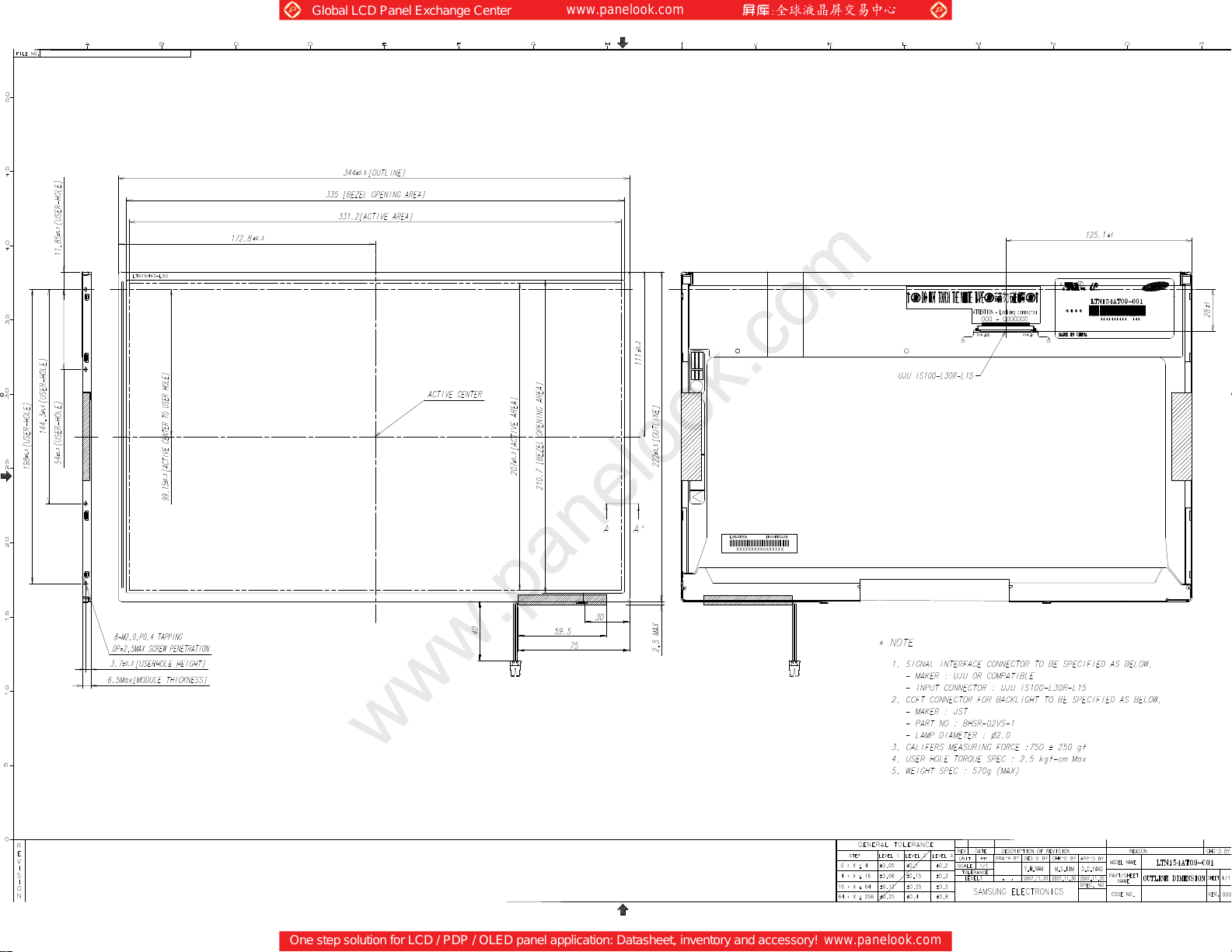
m331.2(H) x 207.0(V) (15.4” diagonal )
m0.2588(H) x 0.2588(V) (TYP.)
D
isplay area
D
river element
D
isplay colors
N
umber of pixel
P
ixel arrangement
P
ixel pitch
a
-Si TFT active matrix
2
62,144
R
GB vertical stripe
NoteUnitSpecificationItem
1
6 : 10pixel1280 x RGB(3) x 800
N
D
isplay Mode
S
urface treatment
amsung Secret
S
oc.No. Rev.No
D
ormally white
0
4-A00-G-080620
Page
G
lareHaze 25, Hard-Coating 3H
31LTN154AT09-8
/
4
Page 5
Global LCD Panel Exchange Center
www.panelook.com
One step solution for LCD / PDP / OLED panel application: Datasheet, inventory and accessory!
www.panelook.com
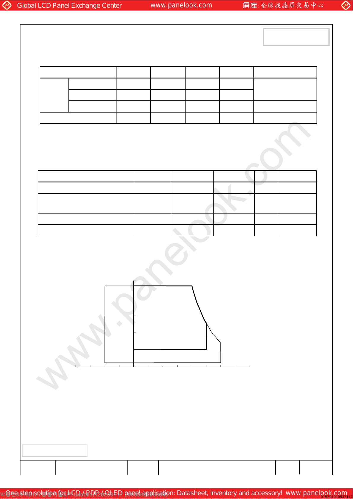
Mechanical Information
A
pproval
Max.
344.5
Module
size
1.
ABSOLUTE MAXIMUM RATINGS
1
.1 ENVIRONMENTAL ABSOLUTE RATINGS
Operating temperate
(Temperature of glass surface)
N
ote (1) Temperature and relative humidity range are shown in the figure below.
95 % RH Max. (40 °C ≥ Ta)
Maximum wet - bulb temperature at 39 OC or less. (Ta > 40 °C ) No condensation
222.5
6.5
70
5
NoteUnitTyp.Min.Item
mm344.0343.5Horizontal (H)
mm222.0221.5Vertical (V)
mm--Depth (D)
w/o inverter ass’y
LCD module onlyg555-Weight
NoteUnitMax.Min.SymbolItem
(1),(5)°C60-20 TSTGStorage temperate
(1),(5)°C500TOPR
(2),(4)G240-SnopShock ( non-operating )
(
3),(4)G2.41-VnopVibration (non-operating)
100
-40 -20 0 20 40 60 80
(2) 2ms, half sine wave, one time for ±X, ±Y, ± Z.
(3) 5 - 500 Hz, random vibration, 30min for X, Y, Z.
(4) At testing Vibration and Shock, the fixture in holding the Module to be tested have to be
hard and rigid enough so that the Module would not be twisted or bent by the fixture.
(5) If product is used for extended time excessively or exposed to high temperatures for extended time,
there is a possibility of wide viewing angle film damage which could affect visual characteristics
Relative Humidity ( %RH)
90
80
60
40
2
0
0
perating Range
O
Storage Range
5
Temperature (
O
C
)
(
40,90 )
( 50,50.4 )
( 60,27.7 )
.
amsung Secret
S
oc.No. Rev.No
D
0
4-A00-G-080620
Page
31LTN154AT09-8
/
5
Page 6
Global LCD Panel Exchange Center
www.panelook.com
One step solution for LCD / PDP / OLED panel application: Datasheet, inventory and accessory!
www.panelook.com
1
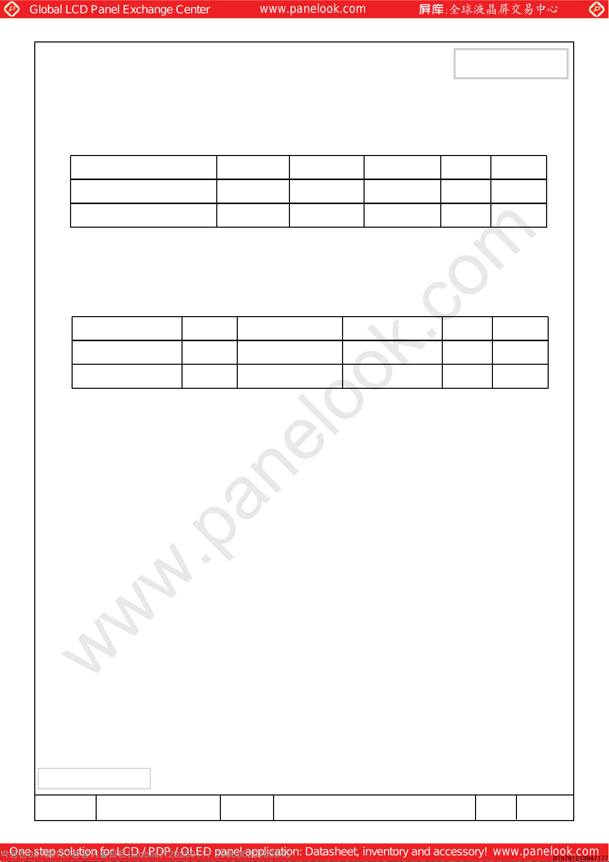
.2 ELECTRICAL ABSOLUTE RATINGS
(1) TFT LCD MODULE
V
D
D
=
3.3V, V
A
pproval
S
=
S
GND = 0V
NoteUnitMax.Min.SymbolItem
D
ower Supply Voltage
P
ogic Input Voltage
L
N
ote (1) Within Ta (25 ± 2 °C )
D
D
D
D
D
0.3V
D
–
D
0.3V
D
–
0.3V
D
+
D
0.3V
D
+
(2) BACK-LIGHT UNIT
amp Current
amp frequency
Note 1) Permanent damage to the device may occur if maximum values are exceeded
Functional operation should be restricted to the conditions described under normal operating conditions.
LL
LL
1)VV
(
(1)VV
Ta = 25 ± 2 °C
NoteUnitMax.Min.SymbolItem
(1)mArms7.03.0I
(1)kHz8040F
amsung Secret
S
oc.No. Rev.No
D
0
4-A00-G-080620
Page
31LTN154AT09-8
/
6
Page 7
Global LCD Panel Exchange Center
www.panelook.com
One step solution for LCD / PDP / OLED panel application: Datasheet, inventory and accessory!
www.panelook.com
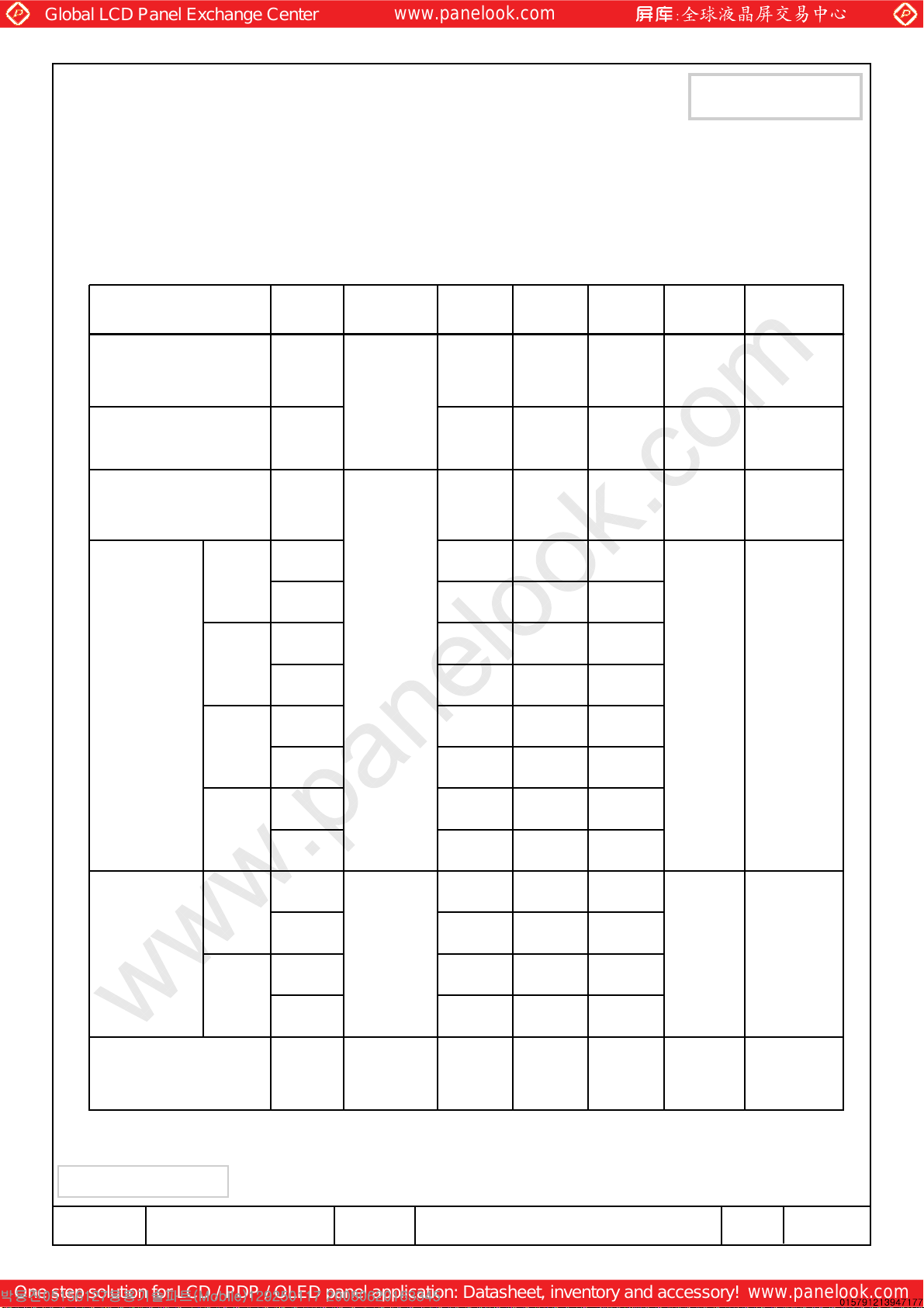
2.
OPTICAL CHARACTERISTICS
T
he following items are measured under stable conditions. The optical characteristics
should be measured in a dark room or equivalent state with the methods shown in Note (5).
Measuring equipment : TOPCON BM-5A and PR-650
A
pproval
Contrast Ratio
(5 Points)
R
esponse Time at Ta
( Rising + Falling )
A
verage Luminance
of White (5 Points)
G
Color
Chromaticity
( CIE )
R
ed
reen
B
lue
*
Ta = 25 ± 2 °C, VDD=3.3V, fv= 60Hz, f
CR
R
T_B/W
L,A
VE
X
R
Y
R
Normal
X
G
Viewing
Angle
Y
G
X
B
Y
B
φ = 0
θ = 0
D
=
CLK
71.26MHz, I
-220200Y
Unit
msec
cd/m
L =
6.0 mArms
NoteMaxTyp.Min.ConditionSymbolItem
-
(1), (2), (5)-500300
(1), (3)2516-T
L=
6.0mA
I
2
(1), (4)
0.6100.5900.570
0.3600.3400.320
0
.3500.3300.310
(
0.5650.5450.525
-
0
.1750.1550.135
1), (5)
PR-650
0.1550.1350.115
X
W
hite
Y
L
θ
H
or.
Viewing
Angle
V
er.
1
3 Points
White Variation
amsung Secret
S
oc.No. Rev.No
D
H
CR ≥ 10
H
L
L
5φ
0
4-A00-G-080620
0
.3330.3130.293W
0.3490.3290.309W
--40
--40θ
--1
Degrees
(
1), (5)
BM-5A
--30φ
-
Page
(6)1.7--δ
31LTN154AT09-8
/
7
Page 8
Global LCD Panel Exchange Center
www.panelook.com
One step solution for LCD / PDP / OLED panel application: Datasheet, inventory and accessory!
www.panelook.com
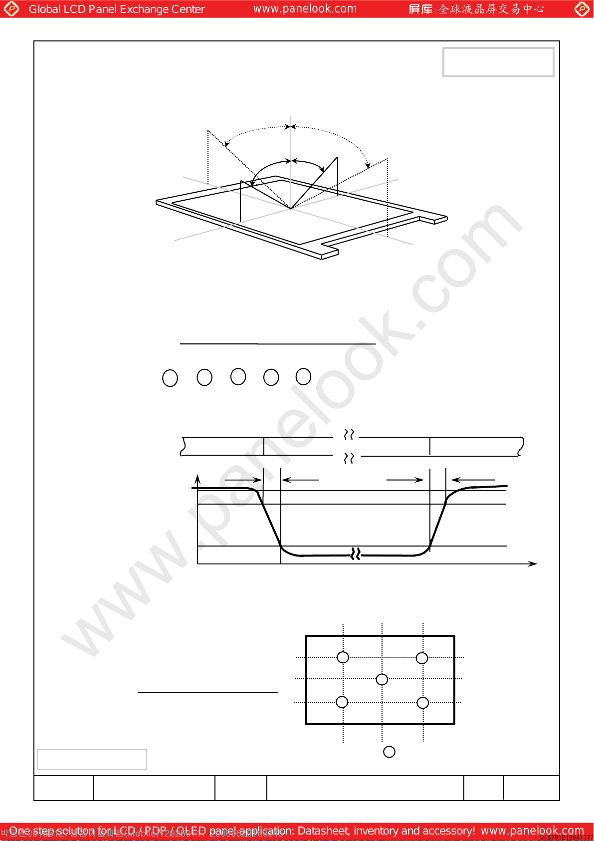
Note 1) Definition of Viewing Angle : Viewing angle range( 10
θL =90
6
O’clock
direction
φL= 90
N
ote 2) Definition of Contrast Ratio (CR) : Ratio of gray max (Gmax) ,gray min (Gmin)
at 5 points(4, 5, 7, 9, 10)
o
x
o
ormal Line
N
o
,
φ = 0
θ L
φ L
φ H
θ =
0
≤
≤
≤
≤
o
/R, 100
C
θ R
A
≤
/R )
≤
C
≤
≤
1
2 O’clock
direction
y
φH= 90
x
'y'
=90
θ
R
pproval
o
o
CR(4) + CR(5) + CR(7) + CR(9) + CR(10)
R =
C
5
Points : , , , , at the figure of Note (6).
ote 3) Definition of Response time :
N
4
Display data
1
00%
5
G
ray 32(TFT OFF) Gray 32(TFT OFF)
White(TFT OFF)
7
9
T
R
0
1
Gray 48 (TFT ON)
B
lack(TFT ON)
hite(TFT OFF)
W
TF
90%
Optical
Response
10%
0%
Note 4) Definition of Average Luminance of White : measure the luminance of white at 5 points.
(320) ( 640) (960)
V
IEW AREA
T
ime
Average Luminance of White ( Y
Y
L4 + YL5 + YL7 + YL9 + YL10
Y
,AVE
L
=
5
,AVE
L
)
1
0
7
5
9
(200)
(400)
4
(600)
(lines)
: test point
amsung Secret
S
oc.No. Rev.No
D
0
4-A00-G-080620
Page
31LTN154AT09-8
/
8
Page 9
Global LCD Panel Exchange Center
www.panelook.com
One step solution for LCD / PDP / OLED panel application: Datasheet, inventory and accessory!
www.panelook.com
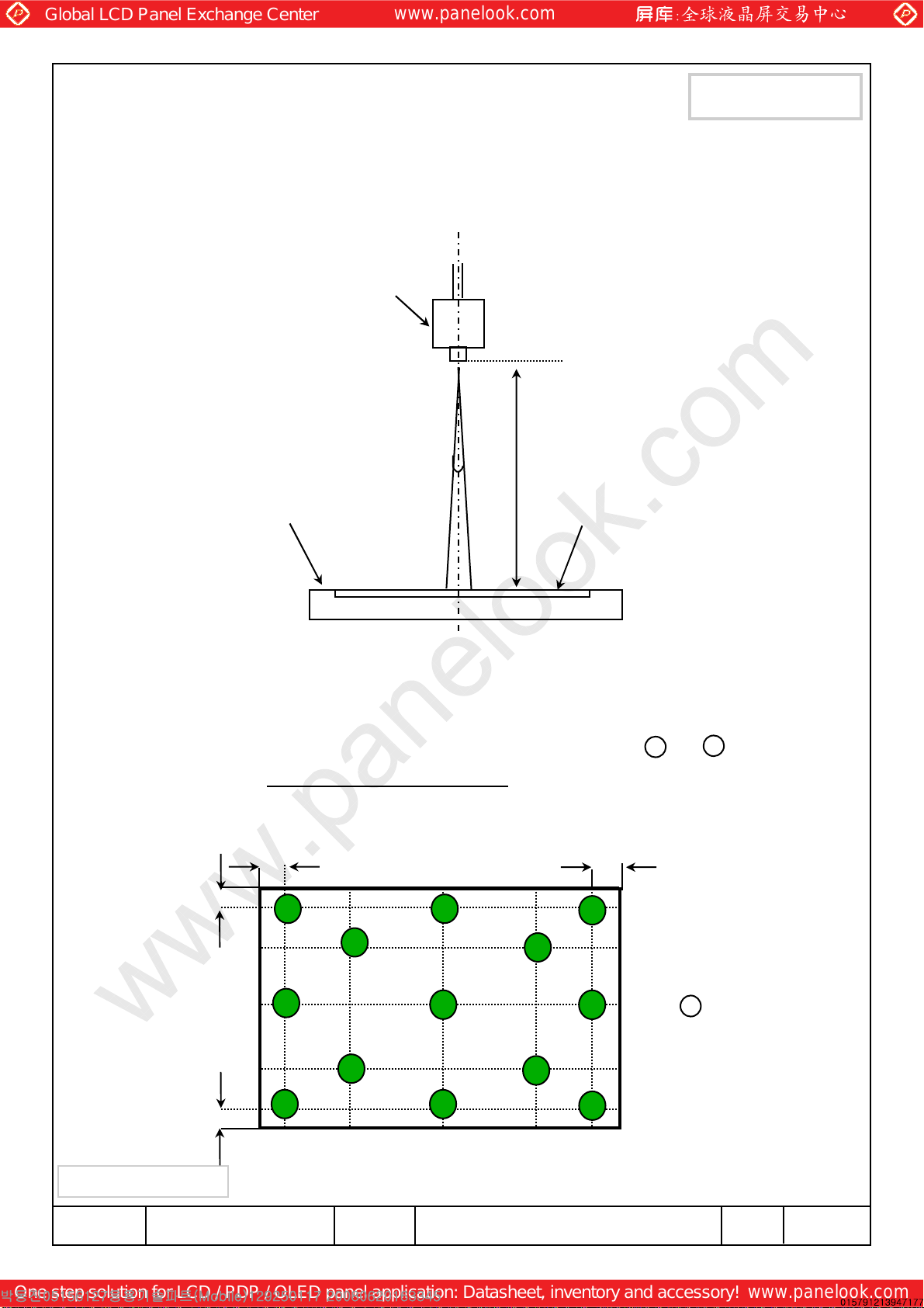
ote 5) After stabilizing and leaving the panel alone at a given temperature for 30 min , the measurement
N
should be executed. Measurement should be executed in a stable, windless,and dark room.
30 min after lighting the backlight. This should be measured in the center of screen.
Lamp current : 6.0mA
Environment condition : Ta = 25 ± 2 °C
P
hoto-detector
( TOPCON BM-5A
PR-650 )
Field
2°
=
0 cm
5
A
pproval
TFT-LCD module
Optical characteristics measurement setup ]
[
N
ote 6) Definition of 13 points white variation (
Maximum luminance of 13 points
δ L =
Minimum luminance of 13 points
0mm
0mm
1
1
1
3
3
20 640
1
0
Center of the screen
δ
L
)
, CR variation( CVER ) [ ~ ]
960
2
1
CD panel
L
1
1
0mm
1
1
9
200
13
8
5
3
10mm
amsung Secret
S
oc.No. Rev.No
D
7
2
0
4-A00-G-080620
6
400
4
1
600
(lines)
:
test point
Page
31LTN154AT09-8
/
9
Page 10
Global LCD Panel Exchange Center
www.panelook.com
One step solution for LCD / PDP / OLED panel application: Datasheet, inventory and accessory!
www.panelook.com
3.
ELECTRICAL CHARACTERISTICS
3
.1 TFT LCD MODULE
A
pproval
a= 25 ± 2°C
T
NoteUnitMax.Typ.Min.SymbolItem
oltage of Power Supply
V
Differential Input
igh
H
D
D
H
I
Voltage for LVDS
D
R
I
I
HH
CLK
USH
D
L
D
Receiver Threshold
sync Frequency
ain Frequency
M
ush Current
R
Current of Power
W
L
ow
hite
Supply
N
ote (1) Display data pins and timing signal pins should be connected.( GND = 0V )
(2) f
V =
60Hz, f
D
=
CLK
71.26MHz, V
D
=
D
3.3V , DC Current.
(3) Power dissipation pattern
V3.63.33.0V
V
M
+1.2VmV+100--V
C
=
mV---100V
Hz-60-fvVsync Frequency
KHz-48.96-f
MHz-71.26-f
(4)A1.5--I
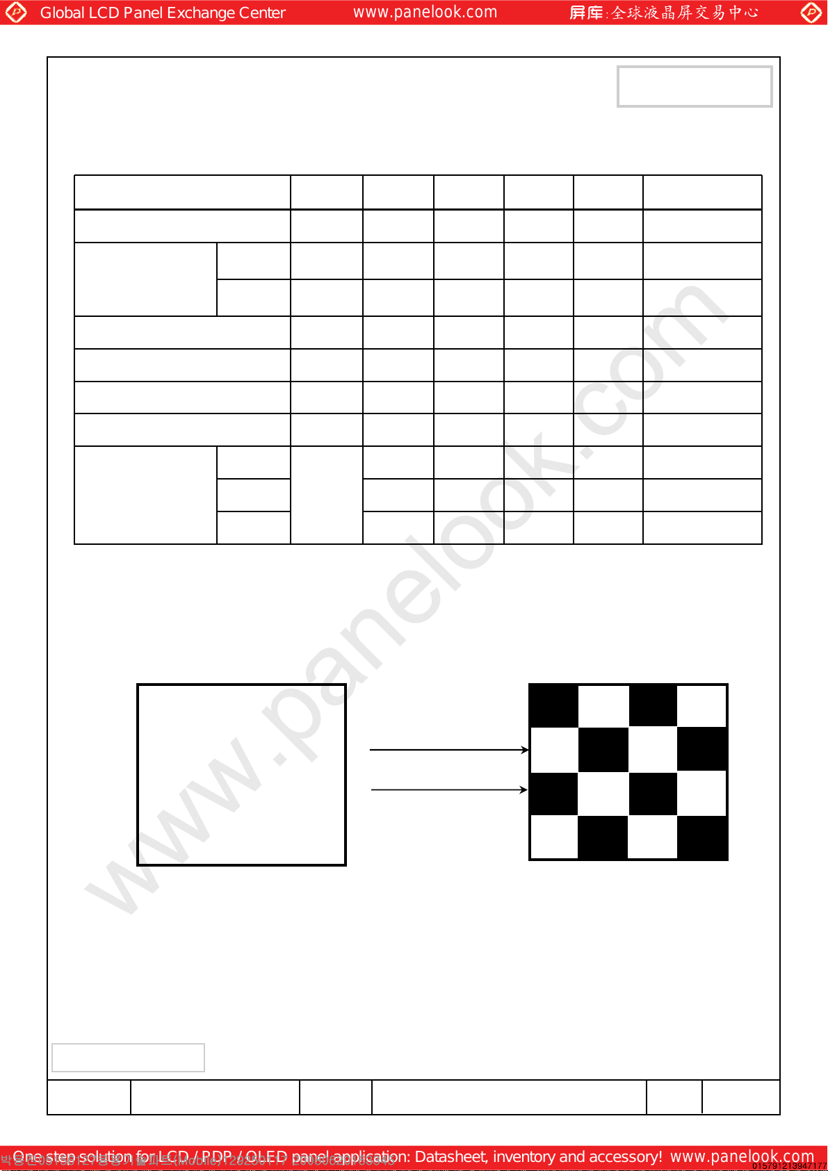
(2),(3)*amA-300(2),(3)*bmA-310-Mosaic
(2),(3)*cmA500380-V. stripe
*a) White Pattern *b) Mosaic Pattern
VIEW AREA
amsung Secret
S
isplay Brightest Gray Level
D
isplay Darkest Gray Level
D
oc.No. Rev.No
D
0
4-A00-G-080620
Page
31LTN154AT09-8
/
10
Page 11
Global LCD Panel Exchange Center
www.panelook.com
One step solution for LCD / PDP / OLED panel application: Datasheet, inventory and accessory!
www.panelook.com
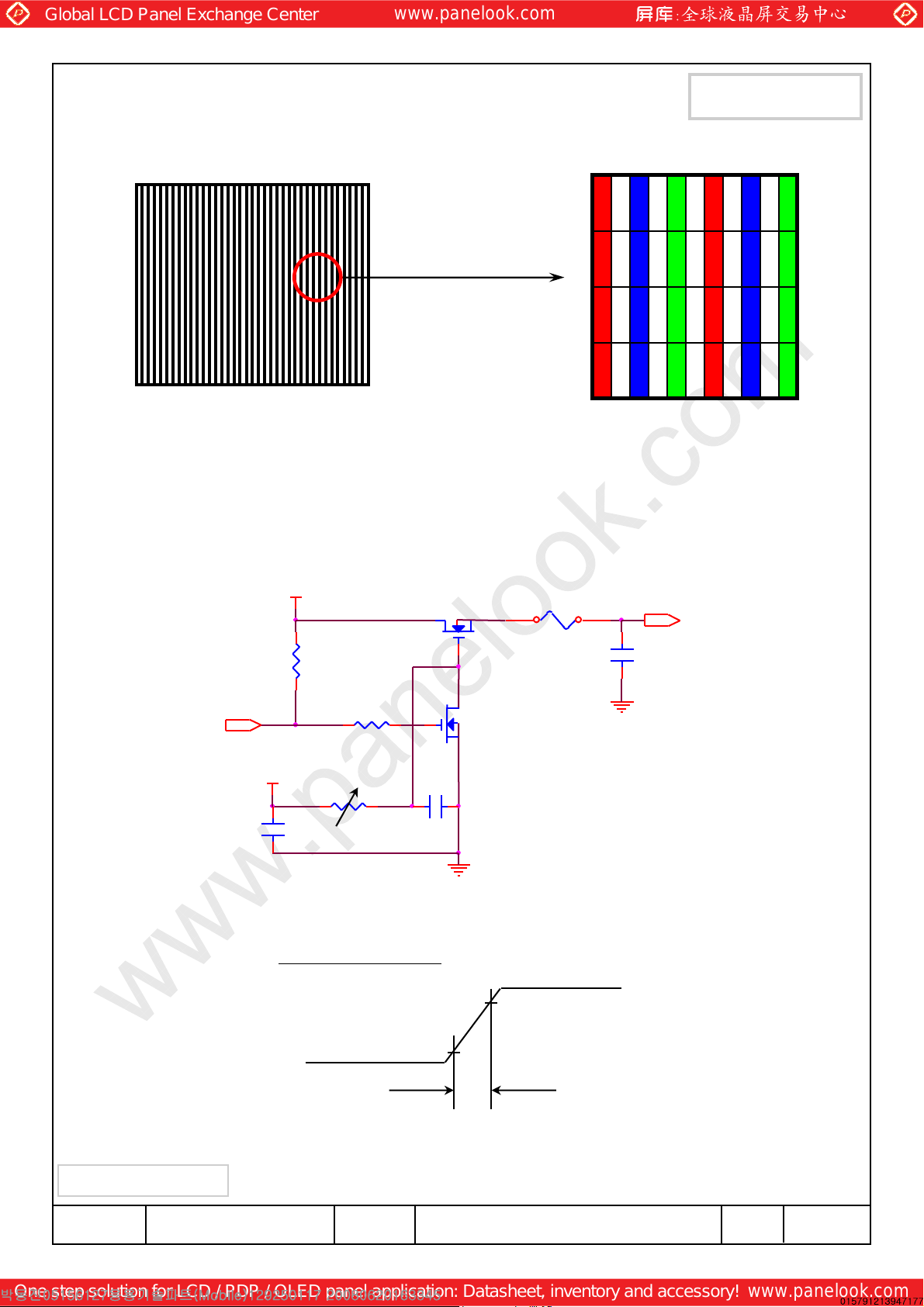
*
c) 1dot Vertical stripe pattern
A
pproval
G B R G B R G B R G
R
G B R G B R G B R G
R
R
G B R G B R G B R G
R G B R G B R G B R G
4) Rush current measurement condition
3.3V
1
R
47K
C
ONTROL SIGNAL
(
HIGH to LOW)
1
2V
3
C
1uF
V
DD rising time is 470us
R
1K
R
3
47K
1
M
2SK1059
D (
CD INPUT)
VD
F
USE
2
C
2
10000pF
.9VDD
0
M
2
2SK1399
3
C
1uF
.3V
1
L
0.1VDD
GND
amsung Secret
S
oc.No. Rev.No
D
0
4-A00-G-080620
470us
Page
31LTN154AT09-8
/
11
Page 12
Global LCD Panel Exchange Center
www.panelook.com
One step solution for LCD / PDP / OLED panel application: Datasheet, inventory and accessory!
www.panelook.com
3
.2 BACK-LIGHT UNIT
The backlight system is an edge-lighting type with a single CCFT ( Cold Cathode Fluorescent Tube ).
The characteristics of a single lamp are shown in the following table.
A
pproval
Ta= 25 ± 2 °C
NoteUnitMax.Typ.Min.SymbolItem
amp Current
amp Voltage
requency
ower Consumption
tartup Voltage
Note) The waveform of the inverter output voltage must be area symmetric and the design of the
inverter must have specifications for the modularized lamp.
The performance of the backlight, for example life time or brightness, is much influenced by the
characteristics of the DC-AC inverter for the lamp. So all the parameters of an inverter should be carefully
designed so as not to produce too much leakage current from high-voltage output of the inverter.
When you design or order the inverter, please make sure that a poor lighting caused by the mismatch of
the backlight and the inverter(miss lighting, flicker, etc.) never occur. When you confirm it, the module
should be operated in the same condition as it is installed in your instrument.
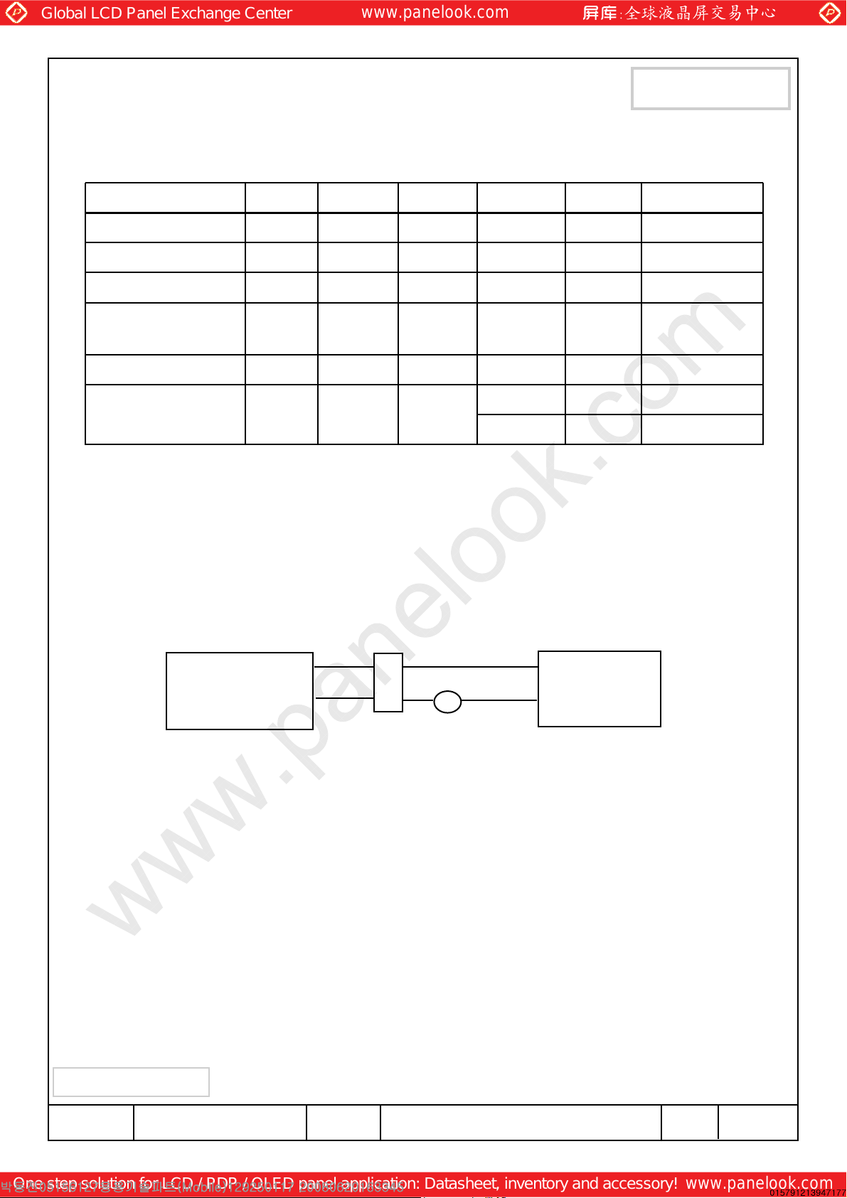
Note (1) Lamp current is measured with a high frequency current meter as shown below.
LL
LL
0f
LF
LP
SS
4
6
0
--V
8
0
W5.04.6-P
I
L
=
I
L
=
25°C, (5)Vrms1250
0°C, (5)Vrms1500
(1)mArms7.06.03.0I
6.0mAVrms-655-V
(2)KHz
(3)
6.0mA
(4)Hour--15,000HrOperating Life Time
(
2) Lamp frequency may produce interference with horizontal synchronous frequency and this
may cause line flow on the display. Therefore lamp frequency should be detached from the
horizontal synchronous frequency and its harmonics as far as possible in order to avoid interference.
(3) Refer to I
(4) Life time (Hr) of a lamp can be defined as the time in which it continues to operate under the
condition Ta= 25 ± 2 °C and I
1. When the brightness becomes 50% or lower than the original.
2. When the Effective ignition length becomes 80% or lower than the original value.
(Effective ignition length is defined as an area that has less than 70% brightness compared to
3. CCFL only
(5) The inverter open voltage - this voltage should be measured after ballast capacitor- have to be larger
than the lamp startup voltage, otherwise backlight may has blinking for a moment after turns on
or not be turned on.
If an inverter has shutdown function it should keep its open voltage for longer than 1 second
even if lamp connector open.
amsung Secret
S
CD
L
MODULE
L ×VL to calculate.
L = 6.0 mA
the brightness in the center point.)
OT : ( PINK )
H
1
COLD : ( White )
2
r
ms
A
u
ntil one of the followingevent occurs.
INVERTER
oc.No. Rev.No
D
0
4-A00-G-080620
Page
31LTN154AT09-8
/
12
Page 13
Global LCD Panel Exchange Center
www.panelook.com
One step solution for LCD / PDP / OLED panel application: Datasheet, inventory and accessory!
www.panelook.com
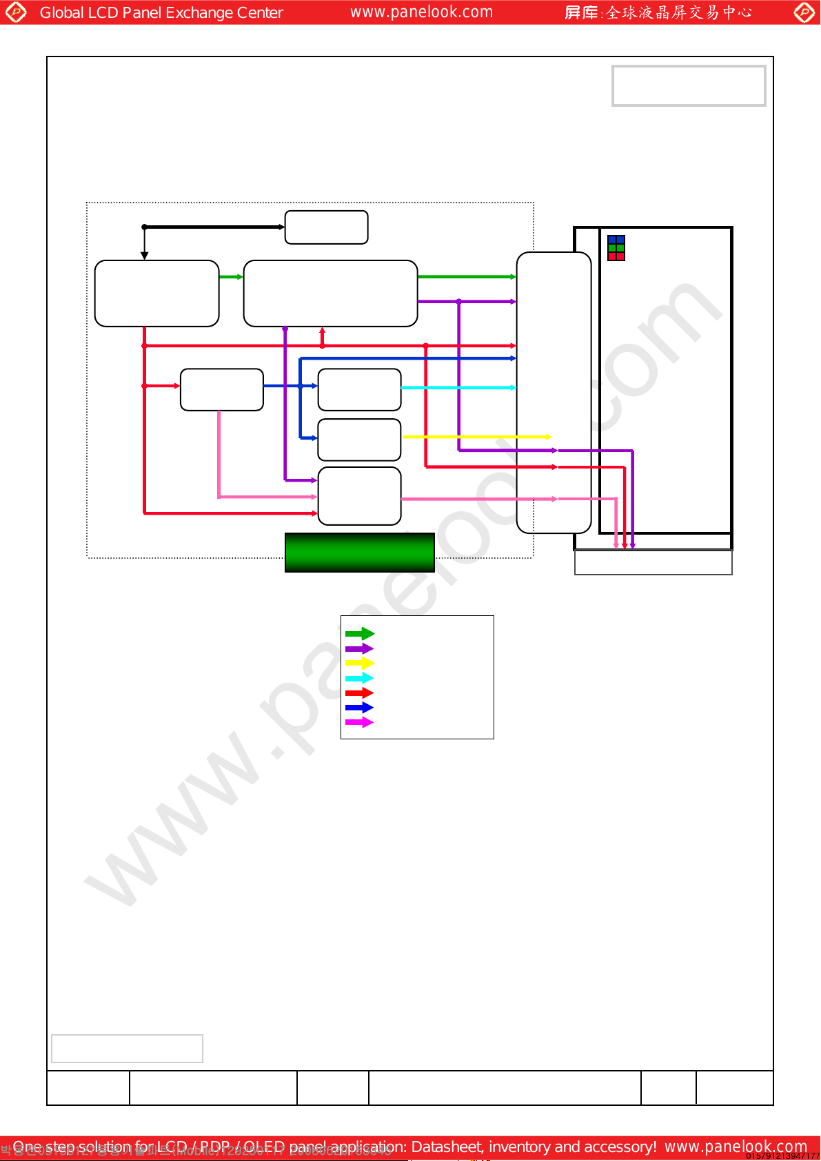
4.
BLOCK DIAGRAM
.1 TFT LCD Module
4
2
C bus
I
L
VDS
U
ser-
Connector
DC-DC
onverter
C
LVDS Input/RSDS Output
E
EDID
EEPROM
Timing Controller
Gamma
Generator
R
SDS
Source
Driver
IC
A
pproval
15.4” WXGA
(1280*3*800)
TFT-LCD Panel
VCOM
Generator
ate Pulse
G
Generator
OURCE PCB
S
Video Signal
C
ontrol Signal
VCOM
Gamma
DVDD
AVDD
Von/Voff
G
ate IC
amsung Secret
S
oc.No. Rev.No
D
0
4-A00-G-080620
Page
31LTN154AT09-8
/
13
Page 14
Global LCD Panel Exchange Center
www.panelook.com
One step solution for LCD / PDP / OLED panel application: Datasheet, inventory and accessory!
www.panelook.com
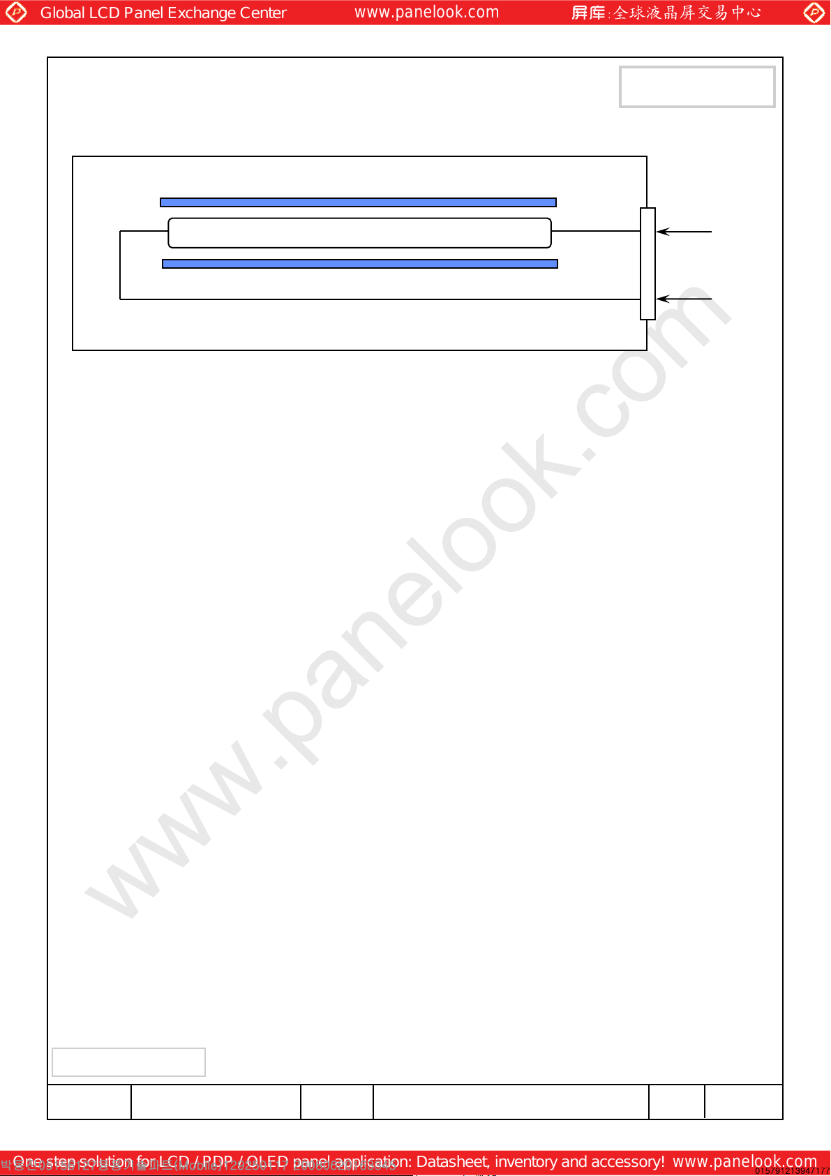
4
.2 BACKLIGHT UNIT
eflector
R
N
ote) The output of the inverter may change according to the material of the reflector.
AMP
L
A
pproval
1
HOT (PINK)
2
C
OLD (White)
amsung Secret
S
oc.No. Rev.No
D
0
4-A00-G-080620
Page
31LTN154AT09-8
/
14
Page 15
Global LCD Panel Exchange Center
www.panelook.com
One step solution for LCD / PDP / OLED panel application: Datasheet, inventory and accessory!
www.panelook.com
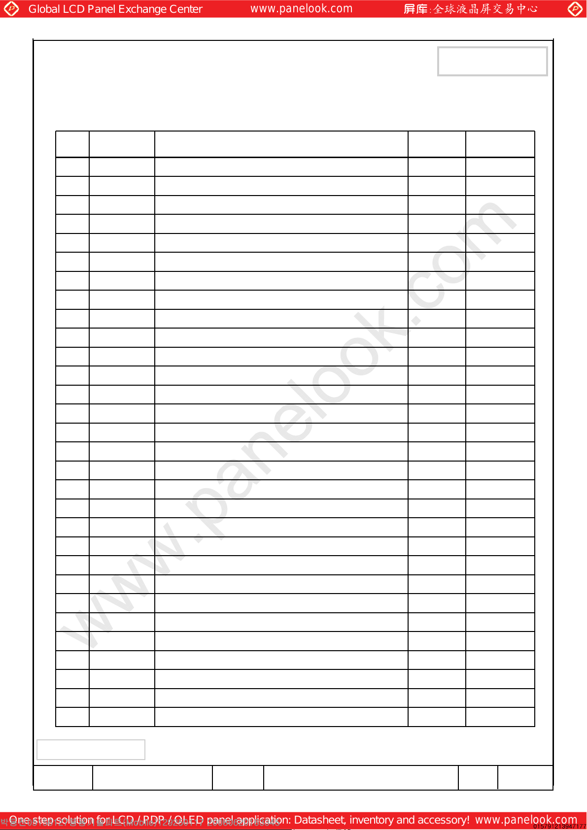
5
. INPUT TERMINAL PIN ASSIGNMENT
.1. Input Signal & Power (LVDS, Connector : JAE FI-XB30SRL-HF11 or compatible )
5
Mating Connector : JAE FI-XB20Sx-HFxx or compatible)
GroundVSS1
POWER SUPPLY +3.3VVDD2
POWER SUPPLY +3.3VVDD3
DDC 3.3V PowerVEEDID4
Panel BIST enableBIST5
DDC ClockCLKEDID6
DDC dataDATAEDID7
A
pproval
RemarksPolarityFunctionSymbolNo.
NegativeLVDS Differential Data INPUT (R0-R5,G0)RxIN0-8
PositiveLVDS Differential Data INPUT (R0-R5,G0)RxIN0+9
GroundGND10
NegativeLVDS Differential Data INPUT (G1-G5,B0-B1)RxIN1-11
PositiveLVDS Differential Data INPUT (G1-G5,B0-B1)RxIN1+12
GroundGND13
NegativeLVDS Differential Data INPUT (B2-B5,Sync,DE)RxIN2-14
PositiveLVDS Differential Data INPUT (B2-B5,Sync,DE)RxIN2+15
GroundVss16
NegativeLVDS Differential Clock INPUTClkIN-17
PositiveLVDS Differential Clock INPUT ClkIN+18
GroundVss19
No connectNC20
No connectNC21
No connectNC22
No connectNC23
o connectNC24
N
No connectNC25
No connectNC26
No connectNC27
No connectNC28
No connectNC29
No connectNC30
amsung Secret
S
oc.No. Rev.No
D
0
4-A00-G-080620
Page
31LTN154AT09-8
/
15
Page 16
Global LCD Panel Exchange Center
www.panelook.com
One step solution for LCD / PDP / OLED panel application: Datasheet, inventory and accessory!
www.panelook.com
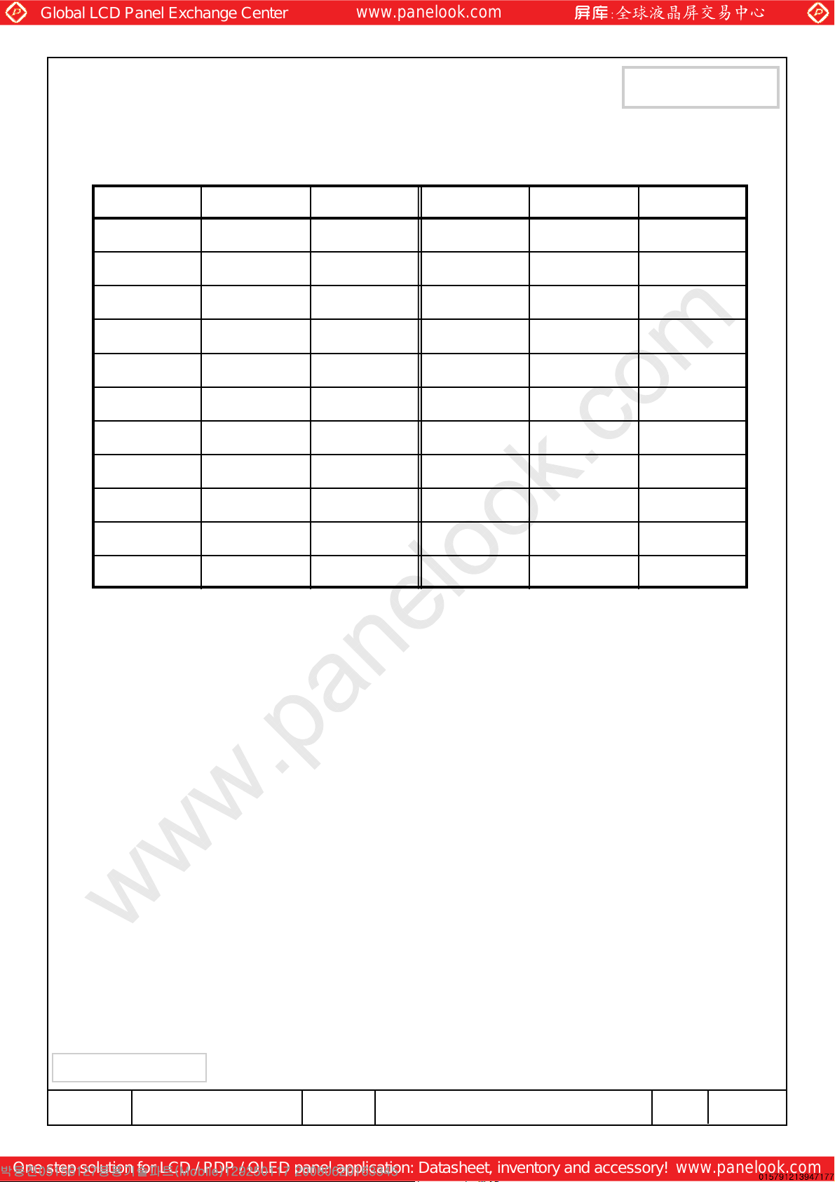
5
.2 LVDS Interface : Transmitter DS90CF363 or Compatible
L
VDS
in No. Name RGB Signal Pin No. Name RGB Signal
P
4
4 TxIN0 RO0 12 TxIN11 GO5
45 TxIN1 RO1 13 TxIN12 BO0
47 TxIN2 RO2 15 TxIN13 BO1
48 TxIN3 RO3 16 TxIN14 BO2
1 TxIN4 RO4 18 TxIN15 BO3
3 TxIN5 RO5 19 TxIN16 BO4
A
pproval
4 TxIN6 GO0 20 TxIN17 BO5
6 TxIN7 GO1 22 TxIN18 Hsync
7 TxIN8 GO2 23 TxIN19 Vsync
9 TxIN9 GO3 25 TxIN20 DE
10 TxIN10 GO4 26 TxCLK IN Clock
amsung Secret
S
oc.No. Rev.No
D
0
4-A00-G-080620
Page
31LTN154AT09-8
/
16
Page 17
Global LCD Panel Exchange Center
www.panelook.com
One step solution for LCD / PDP / OLED panel application: Datasheet, inventory and accessory!
www.panelook.com
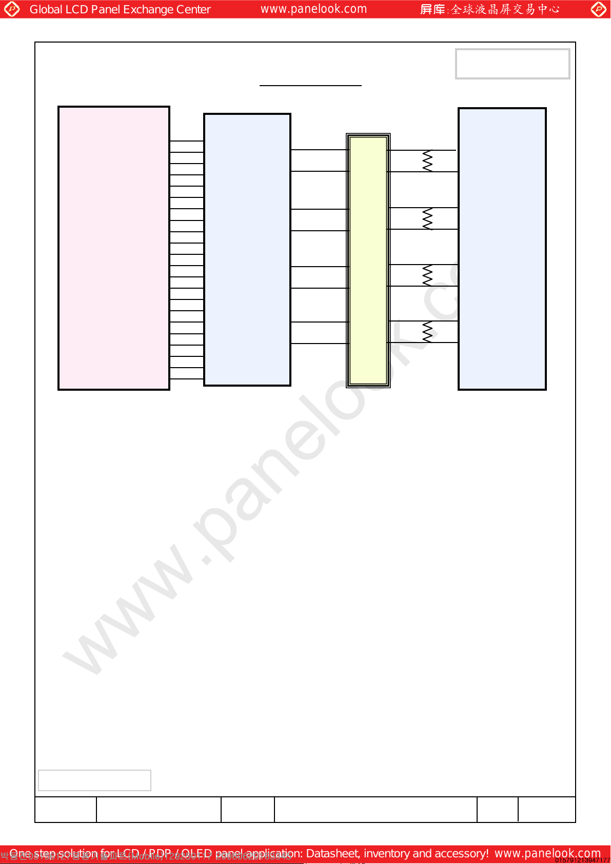
raphics controller
G
18-bit
ED0
R
RED1
RED2
RED3
RED4
RED5
GREEN0
GREEN1
GREEN2
GREEN3
GREEN4
GREEN5
BLUE0
BLUE1
BLUE2
BLUE3
BLUE4
BLUE5
Hsync
Vsync
Enable
CLOCK
L
S90CF363 or
D
compatible
44
45
47
48
1
3
4
6
7
9
10
12
13
15
16
18
19
20
22
23
25
26
TxOUT0-
TxOUT0+
TxOUT1-
TxOUT1+
TxOUT2-
TxOUT2+
TxCLKOUTTxCLKOUT+
VDS Interface
AE,FI-XB30SLR-HF11
J
41
40
39
38
35
34
33
32
8
9
11
12
14
15
17
18
100 Ω
100 Ω
100 Ω
100 Ω
A
pproval
RxIN0RxIN0+
RxIN1RxIN1+
RxIN2RxIN2+
RxCLKRxCLK+
N
ote : The LCD Module uses a 100ohm resistor between positive and negative lines of each
receiver input.
amsung Secret
S
oc.No. Rev.No
D
0
4-A00-G-080620
Page
31LTN154AT09-8
/
17
Page 18
Global LCD Panel Exchange Center
www.panelook.com
One step solution for LCD / PDP / OLED panel application: Datasheet, inventory and accessory!
www.panelook.com
5
.3 BACK LIGHT UNIT
5
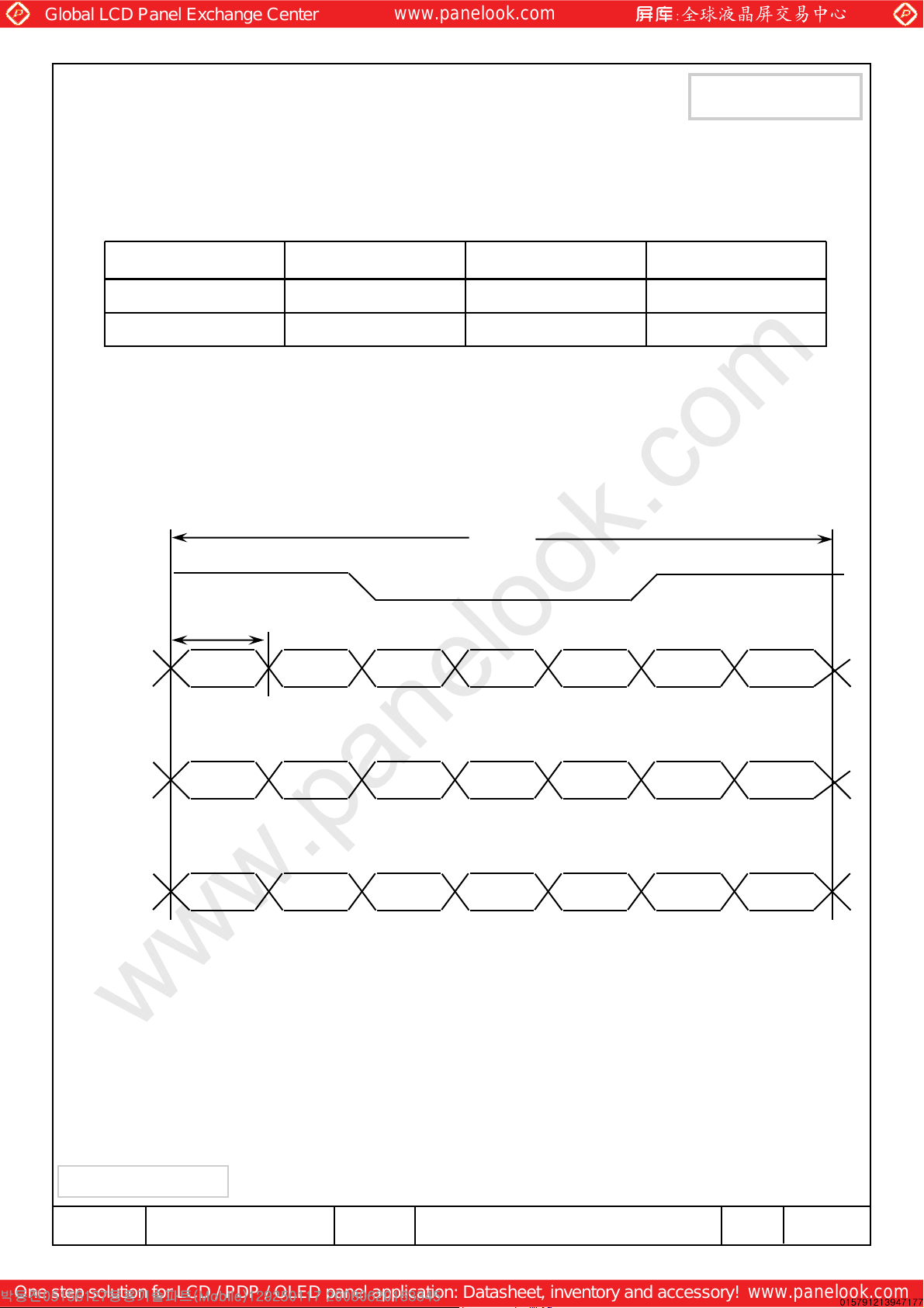
.4 Timing Diagrams of LVDS For Transmission
Mating Connector : SM02B-BHSS-1(JST)
A
pproval
C
onnector : JST BHSR - 02VS -1
FunctionColorSymbolPin NO.
High VoltagePinkHOT1
L
ow VoltageWhiteCOLD2
LVDS Receiver : Integrated T-CON
TxCLK OUT
RxCLK IN
Rx IN2
Rx IN1
RxIN0
T
T
/7
xOUT20 RxOUT19 RxOUT17RxOUT18 RxOUT16 RxOUT15 RxOUT14
R
DE
xOUT13 RxOUT12 RxOUT10RxOUT11 RxOUT9 RxOUT8 RxOUT7
R
R
xOUT6 RxOUT5 RxOUT3RxOUT4 RxOUT2 RxOUT1 RxOUT0
Vsync B2Hsync B5 B3B4
G4B1 G5B0 G3 G2 G1
G0
amsung Secret
S
oc.No. Rev.No
D
R5
R4
R
3
0
4-A00-G-080620
R2 R1 R0
Page
31LTN154AT09-8
/
18
Page 19
Global LCD Panel Exchange Center
www.panelook.com
One step solution for LCD / PDP / OLED panel application: Datasheet, inventory and accessory!
www.panelook.com
5
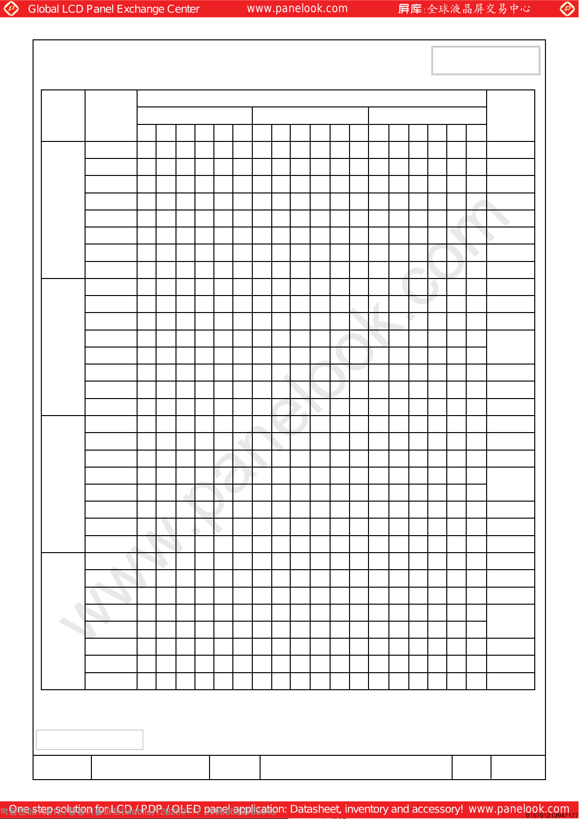
.5 Input Signals, Basic Display Colors and Gray Scale of Each Color
A
pproval
Basic
Colors
Gray
Scale
Of
Red
Data Signal
DisplayColor
BlueGreenRed
B545B3B2B1B0G5G4G3G2G1G0R5R4R3R2R1R0
Gray
Scale
Level
-000000000000000000Black
-111111000000000000Blue
-000000111111000000Green
-111111111111000000Cyan
-000000000000111111Red
-111111000000111111Magenta
-000000111111111111Yellow
-111111111111111111White
R0000000000000000000Black
R1000000000000000001Dark
R2000000000000000010↑
:::::::::::::::::::
R3∼R60
:::::::::::::::::::
R61000000000000111101↓
Gray
Scale
Of
Green
Gray
Scale
Of
Blue
R62000000000000111110Light
R63000000000000111111Red
G0000000000000000000Black
G1000000000001000000Dark
G2000000000010000000↑
:::::::::::::::::::
G3∼G60
:::::::::::::::::::
G61000000111101000000↓
G62000000111110000000Light
G63000000111111000000Green
B0000000000000000000Black
B1000001000000000000Dark
B2000010000000000000↑
:::::::::::::::::::
B3∼B60
:::::::::::::::::::
B61111101000000000000↓
B62111110000000000000Light
N
ote 1) Definition of gray :
Rn: Red gray, Gn: Green gray, Bn: Blue gray (n=gray level)
Note 2)Input signal: 0 =Low level voltage, 1=High level voltage
amsung Secret
S
oc.No. Rev.No
D
0
4-A00-G-080620
Page
B63111111000000000000Blue
31LTN154AT09-8
/
19
Page 20
Global LCD Panel Exchange Center
www.panelook.com
One step solution for LCD / PDP / OLED panel application: Datasheet, inventory and accessory!
www.panelook.com
5
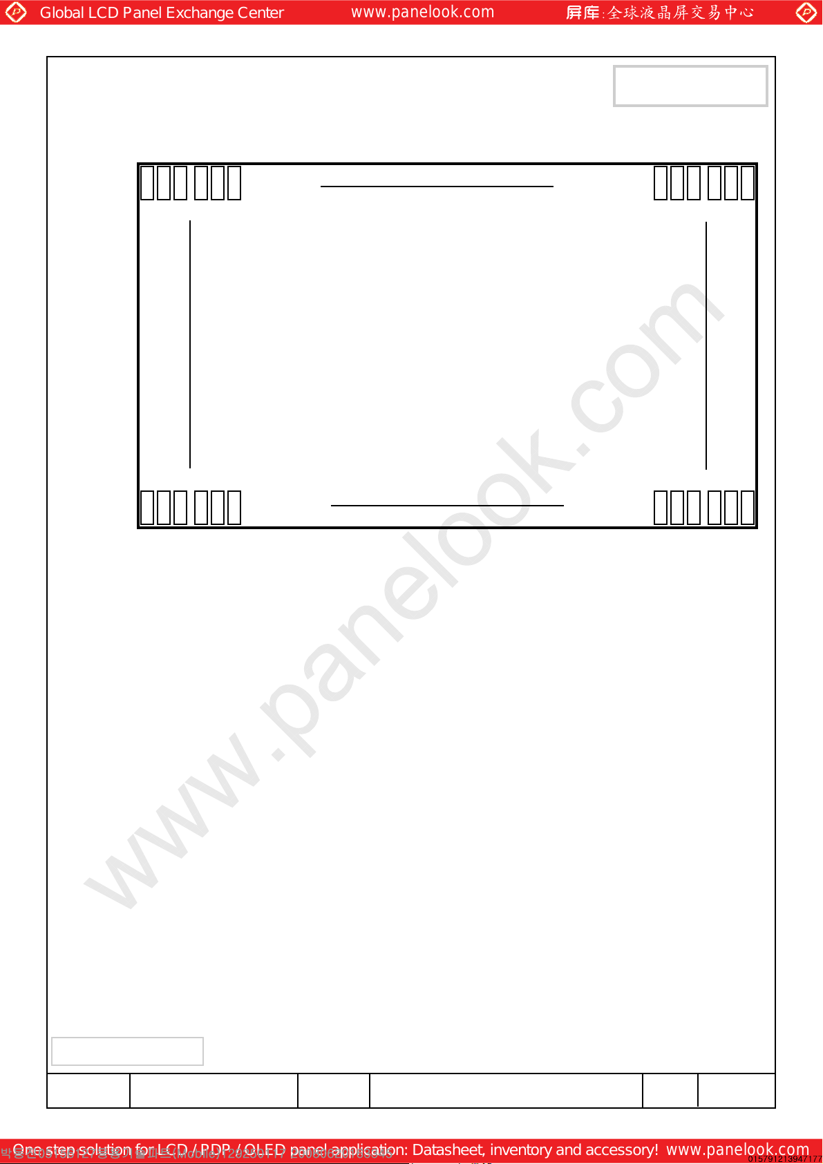
.6 Pixel Format in the display
A
pproval
L
ine 1
Line 800
G B
G B
1280
R
R
G B
G B
1
G B
R
G B
R
L
TN154AT09-8 Panel
G B
G B
R
R
R
R
amsung Secret
S
oc.No. Rev.No
D
0
4-A00-G-080620
Page
31LTN154AT09-8
/
20
Page 21
Global LCD Panel Exchange Center
www.panelook.com
One step solution for LCD / PDP / OLED panel application: Datasheet, inventory and accessory!
www.panelook.com
6
. INTERFACE TIMING
6.1 Timing Parameters
A
pproval
Lines1000816804TVCycleFrame Frequency
NoteUnitMax.Typ.Min.SymbolItemSignal
Vertical Active
Display Term
One Line
Scanning Time
Horizontal Active
Display Term
Display
Period
Display
Period
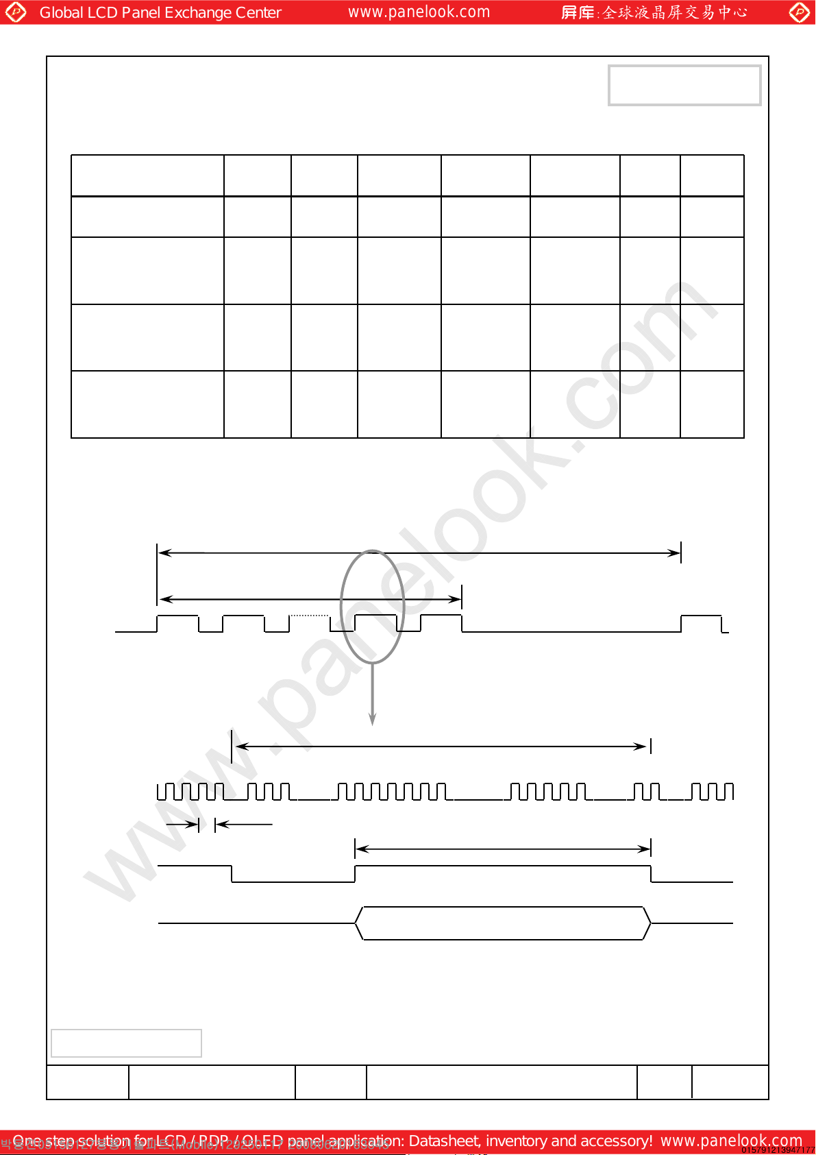
6.2 Timing diagrams of interface signal
D
TV
D
E
TV
Lines-800-TVD
Clocks155014001350THCycle
C
locks-1280-THD
DCLK
TC
DE
DATA
SIGNALS
amsung Secret
S
oc.No. Rev.No
D
TH
TH
D
alid display data ( 1280 clocks)
V
0
4-A00-G-080620
Page
21
31LTN154AT09-8
/
Page 22
Global LCD Panel Exchange Center
www.panelook.com
One step solution for LCD / PDP / OLED panel application: Datasheet, inventory and accessory!
www.panelook.com
6
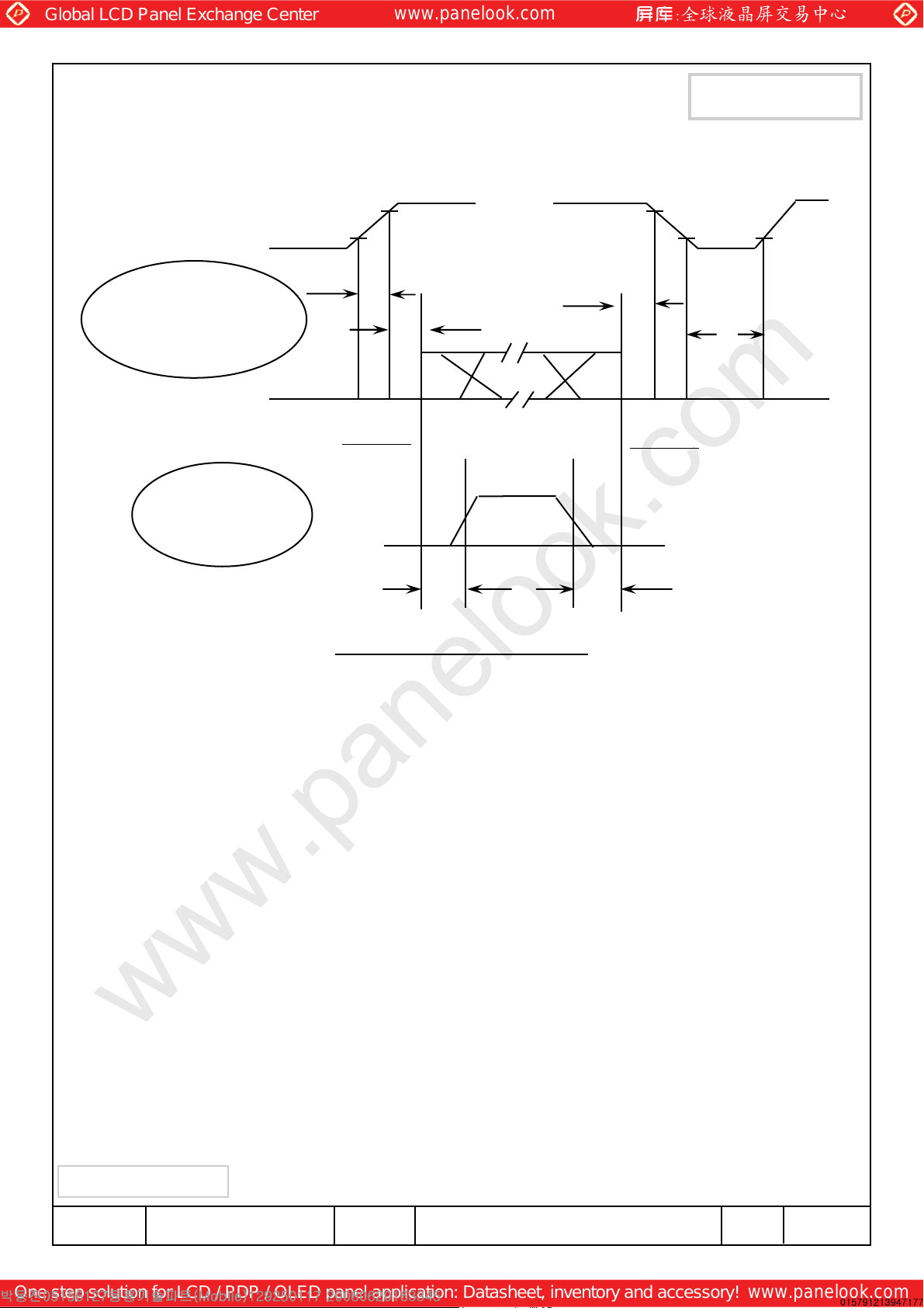
.3 Power ON/OFF Sequence
: To prevent a latch-up or DC operation of the LCD module, the power on/off sequence
should be as the diagram below.
A
pproval
Power Supply
.5 <<<< T
0
0 <<<< T
0 <<<< T
≤ 10 msec
1
≤
≤
≤
≤ 50 msec
2
≤
≤
≤
≤ 50 msec
3
≤
≤
≤
500 msec ≤≤≤≤ T
ack-light
B
200 msec ≤≤≤≤ T
00 msec ≤≤≤≤ T
2
V
0
4
0 V
D
V
D
S
5
6
.1 V
0
ignals
.9 V
D
0
D
D
D
T1
T2
P
ower On
0% 50%
5
T5
Pow
er ON/OFF Sequence
VALID
T6
T3
ower Off
P
0
.9 V
D
0
D
.1 V
T4
D
D
1 : Vdd rising time from 10% to 90%
T
T2 : The time from Vdd to valid data at power ON.
T3 : The time from valid data off to Vdd off at power Off.
T4 : Vdd off time for Windows restart
T5 : The time from valid data to B/L enable at power ON.
T6 : The time from valid data off to B/L disable at power Off.
NOTE.
(1) The supply voltage of the external system for the module input should be the same
as the definition of V
(
2) Apply the lamp voltage within the LCD operation range. When the back-light turns on
D
.
D
before the LCD operation or the LCD turns off before the back-light turns off, the
display may momentarily become white.
D
(3) In case of V
=
D
off level, please keep the level of input signals on the low or keep
a high impedance.
(4) T4 should be measured after the module has been fully discharged between power
off and on period.
(5) Interface signal shall not be kept at high impedance when the power is on.
amsung Secret
S
oc.No. Rev.No
D
0
4-A00-G-080620
Page
31LTN154AT09-8
/
22
Page 23
Global LCD Panel Exchange Center
www.panelook.com
One step solution for LCD / PDP / OLED panel application: Datasheet, inventory and accessory!
www.panelook.com
Page 24
Global LCD Panel Exchange Center
www.panelook.com
One step solution for LCD / PDP / OLED panel application: Datasheet, inventory and accessory!
www.panelook.com
8
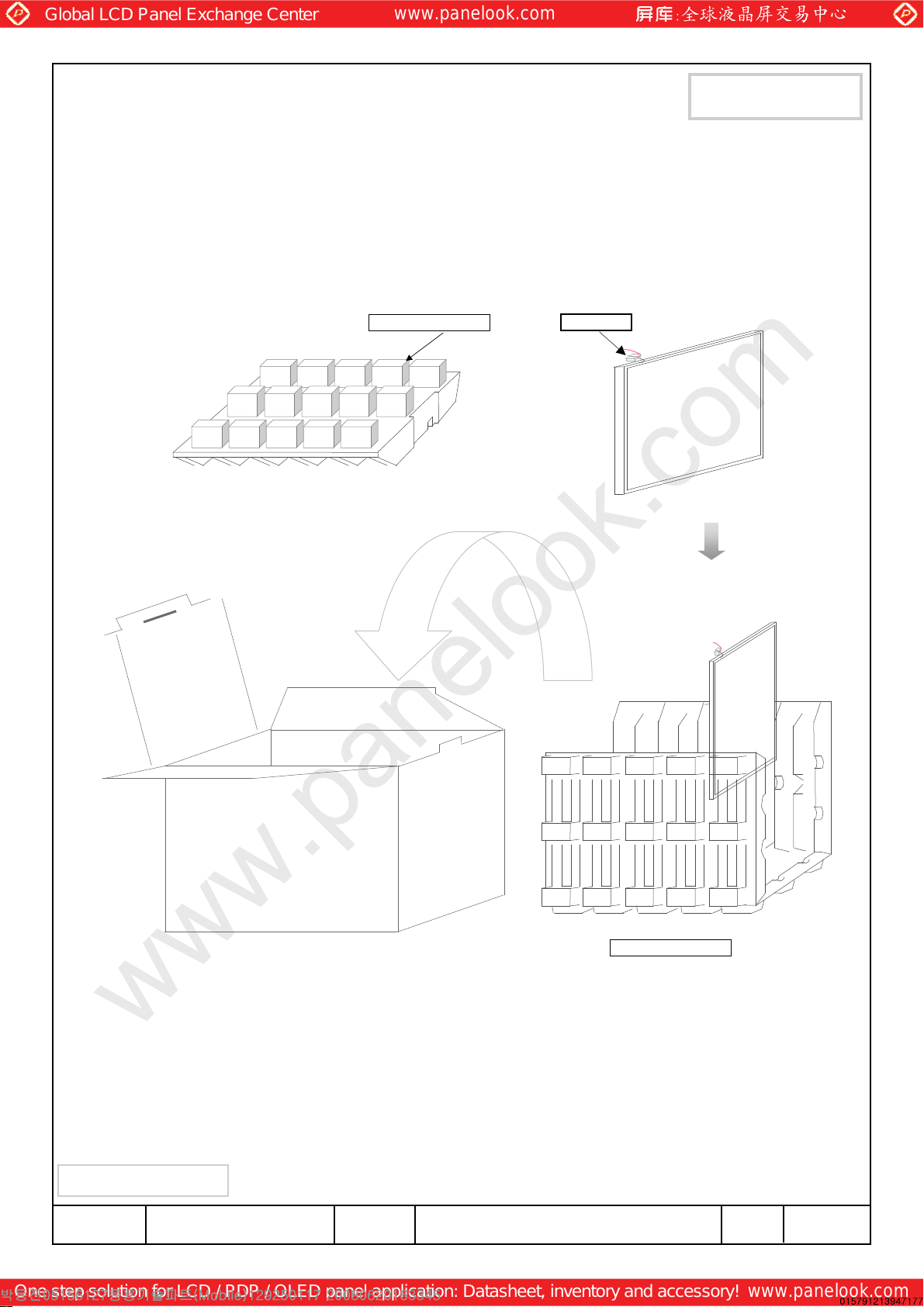
. PACKING
1. CARTON(Internal Package)
(1) Packing Form
Corrugated Cardboard box and Corrupad form as shock absorber
(2) Packing Method
C
USHION CAP
ANEL
P
A
pproval
C
USHION PAD
Note 1)Total Weight : Approximately 10 kg
2) Acceptance number of piling : 10 sets
3) Carton size : 408(W) X 325(D) X 295(H)
amsung Secret
S
oc.No. Rev.No
D
0
4-A00-G-080620
Page
31LTN154AT09-8
/
24
Page 25
Global LCD Panel Exchange Center
www.panelook.com
One step solution for LCD / PDP / OLED panel application: Datasheet, inventory and accessory!
www.panelook.com
QuantityPart nameNo
10Static electric protective sack1
A
pproval
2
Packing case (Inner box)
included shock absorber
1 set
2 pcsPictorial marking3
1
setCarton4
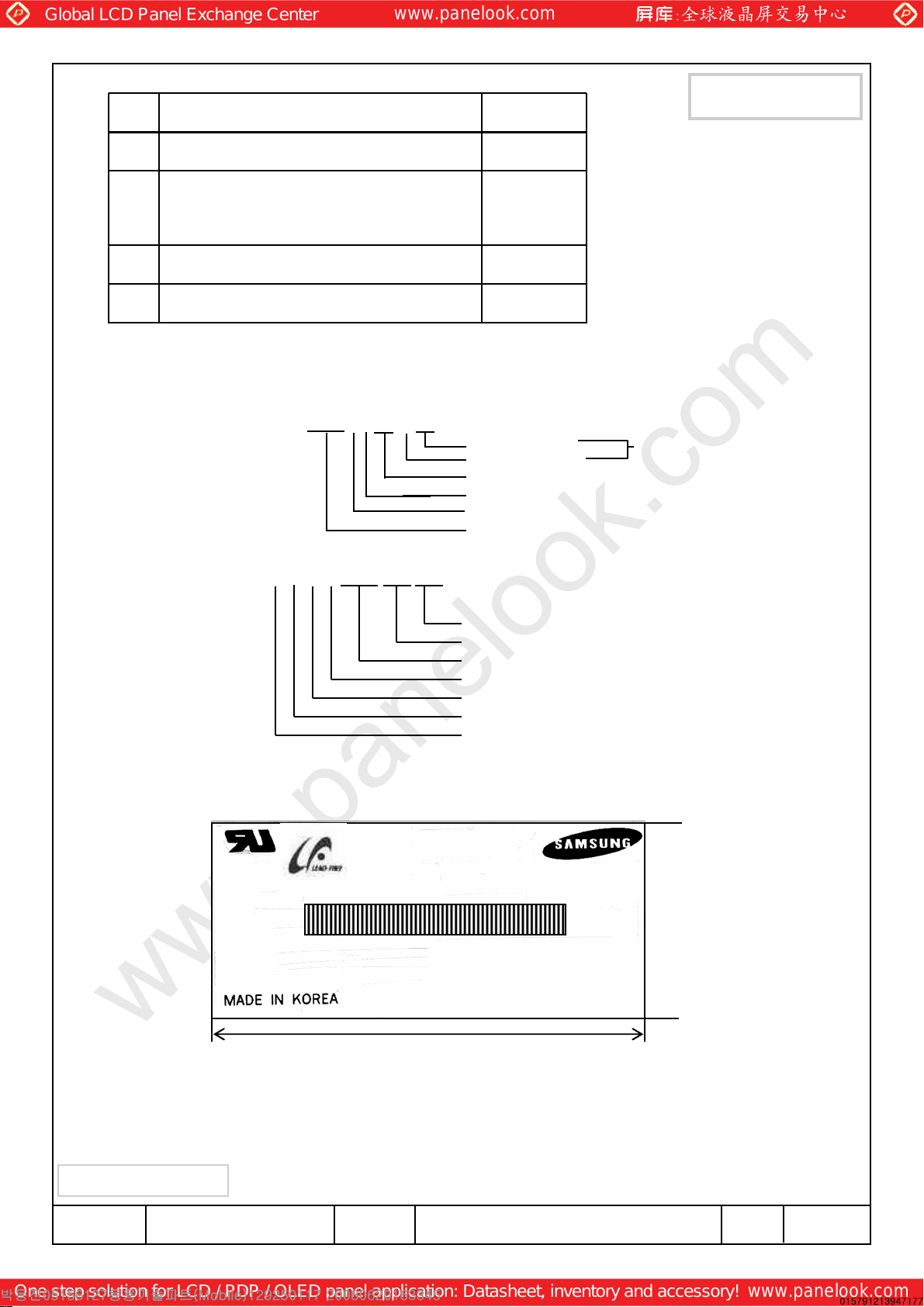
9. MARKINGS & OTHERS
A nameplate bearing followed by is affixed to a shipped product at the
specified location on each product.
(1) Parts number : LTNXXXXXXX-XXX
P
roduct code.
Customer code.
Generation
Tech, information
Resolution
Size
xtension code.
e
(2) Revision : Three letters
(3) Lot number : X Y 7 A XXX XX X
C
ell Position No.(In the one Glass)
Glass No.(In the one Lot)
Lot No.(Glass)
Month
Year(Note 1)
Product Code
Line
N
OTE 1). This code indicating year is omitted in the products of KIHENG site.
5) Nameplate Indication( Following example is only for reference )
(
0
810
X
arts name : LTN154AT09
P
Lot number : XXXXXXXXXX
Inspected work week : 0810(2008 year 10th week)
Product Revision Code : 801
amsung Secret
S
oc.No. Rev.No
D
L
TN154AT09
XXXXXXXXX
8
0 mm
0
01
8
4-A00-G-080620
4
0 mm
Page
25
31LTN154AT09-8
/
Page 26
Global LCD Panel Exchange Center
www.panelook.com
One step solution for LCD / PDP / OLED panel application: Datasheet, inventory and accessory!
www.panelook.com
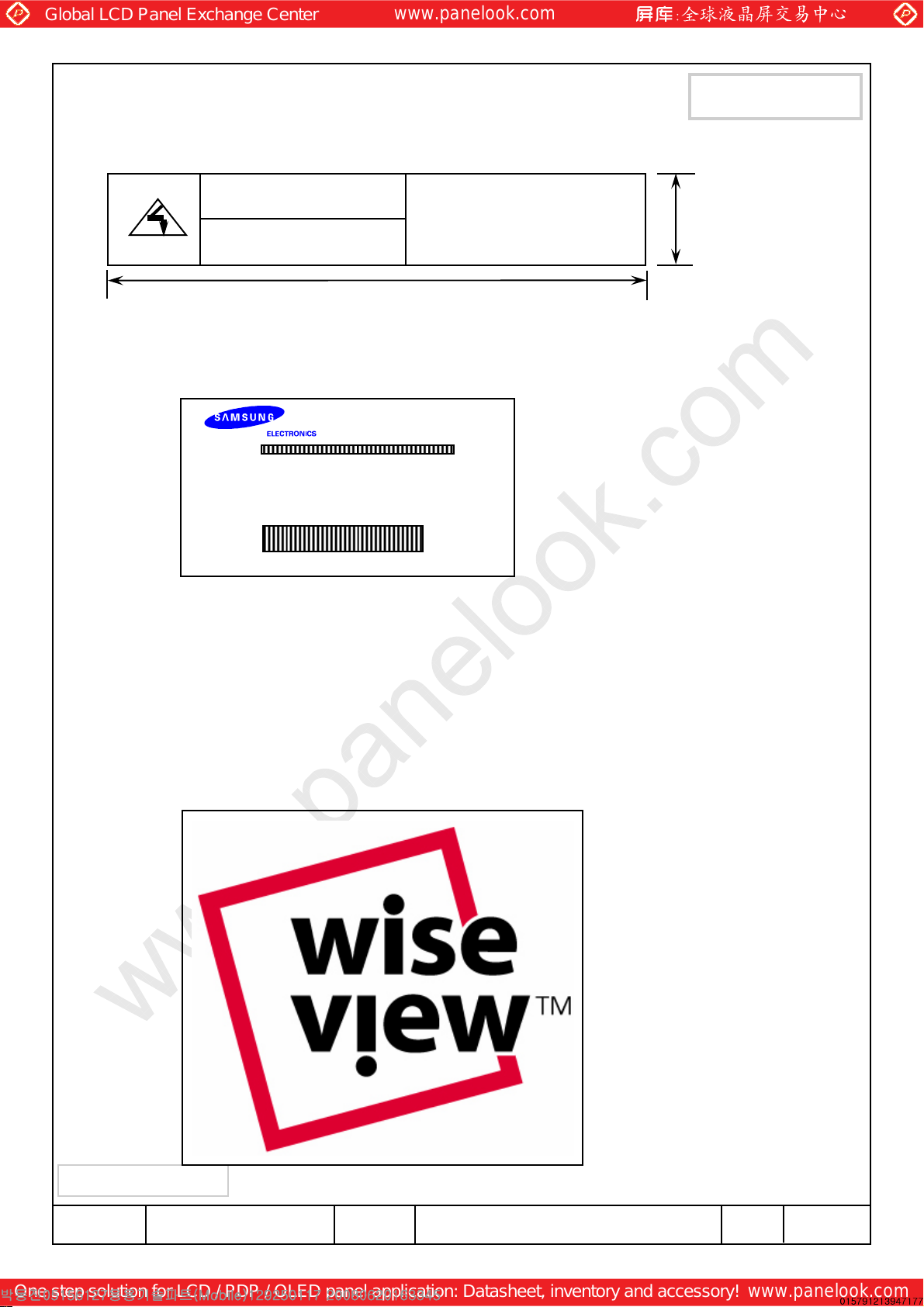
his HIGH VOLTAGE CAUTION is carved in mold frame
T
A
pproval
HIGH VOLTAGE
CAUTION
ISK OF ELECTRIC SHOCK
R
DISCONNECT THE ELECTRIC
POWER BEFORE SERVICE
(
6) Packing box attach
D
EVICE : LTN154AT09
TYPE : XXX
QUANTITY : 10 PCS
C
O6040001
HIS COVER CONTAINS
T
FLUORESCENT LAMP.
PLEASE FOLLOW LOCAL
ORDINANCES OR
REGULATIONS FOR ITS DISPOSAL
7
0mm
1
0mm
High voltage
caution
7) Packing box Marking : Samsung TFT-LCD Brand Name
(
amsung Secret
S
oc.No. Rev.No
D
0
4-A00-G-080620
Page
31LTN154AT09-8
/
26
Page 27
Global LCD Panel Exchange Center
www.panelook.com
One step solution for LCD / PDP / OLED panel application: Datasheet, inventory and accessory!
www.panelook.com
10
. GENERAL PRECAUTIONS
1
. Handling
(a) When the module is assembled, It should be attached to the system firmly
using every mounting holes. Be careful not to twist and bend the modules.
(b) Refrain from strong mechanical shock and / or any force to the module. In addition to
damage, this may cause improper operation or damage to the module and CCFT back-light.
(c) Note that polarizers are very fragile and could be easily damaged. Do not press or scratch
the surface harder than a HB pencil lead.
(d) Wipe off water droplets or oil immediately. If you leave the droplets for a long time,
Staining and discoloration may occur.
A
pproval
(e) If the surface of the polarizer is dirty, clean it using some absorbent cotton or soft cloth.
(f) The desirable cleaners are water, IPA (Isoprophyl Alcohol) or Hexane.
Do not use Ketone type materials(ex. Acetone), Ethyl alcohol, Toluene, Ethyl acid or Methyl
chloride. It might permanent damage to the polarizer due to chemical reaction.
(g) If the liquid crystal material leaks from the panel, it should be kept away from the eyes or
mouth . In case of contact with hands, legs or clothes, it must be washed away thoroughly
with soap.
(h) Protect the module from static , it may cause damage to the C-MOS Gate Array IC.
(i) Use fingerstalls with soft gloves in order to keep display clean during the incoming
inspection and assembly process.
(j) Do not disassemble the module.
(k) Do not pull or fold the lamp wire.
(l) Do not adjust the variable resistor which is located on the back side.
(m) Protection film for polarizer on the module shall be slowly peeled off just before use so
that the electrostatic charge can be minimized.
(n) Pins of I/F connector shall not be touched directly with bare hands.
amsung Secret
S
oc.No. Rev.No
D
0
4-A00-G-080620
Page
31LTN154AT09-8
/
27
Page 28
Global LCD Panel Exchange Center
www.panelook.com
One step solution for LCD / PDP / OLED panel application: Datasheet, inventory and accessory!
www.panelook.com
2
. STORAGE
(a) Do not leave the module in high temperature, and high humidity for a long time.
It is highly recommended to store the module with temperature from 0 to 35 °C and
relative humidity of less than 70%.
(b) Do not store the TFT-LCD module in direct sunlight.
(c) The module shall be stored in a dark place. It is prohibited to apply sunlight or fluorescent
light during the store.
3. OPERATION
(a) Do not connect,disconnect the module in the “ Power On” condition.
(b) Power supply should always be turned on/off by following item 6.3
“ Power on/off sequence “.
A
pproval
(c) Module has high frequency circuits. Sufficient suppression to the electromagnetic
interference shall be done by system manufacturers. Grounding and shielding methods
may be important to minimize the interference.
(d) The cable between the back-light connector and its inverter power supply shall be a
minimized length and be connected directly . The longer cable between the back-light
and the inverter may cause lower luminance of lamp(CCFT) and may require higher
startup voltage (Vs).
(e) The standard limited warranty is only applicable when the module is used for general
notebook applications. If used for purposes other than as specified, SEC is not to be
held reliable for the defective operations. It is strongly recommended to contact SEC
to find out fitness for a particular purpose.
4. OTHERS
(a) Ultra-violet ray filter is necessary for outdoor operation.
(b) Avoid condensation of water. It may result in improper operation or disconnection
of electrode.
(c) Do not exceed the absolute maximum rating value. ( the supply voltage variation, input
voltage variation, variation in part contents and environmental temperature, so on)
Otherwise the module may be damaged.
(d) If the module displays the same pattern continuously for a long period of time,it can be
the situation when the image “sticks” to the screen.
(e) This module has its circuitry PCB’s on the rear side and should be handled carefully in
order not to be stressed.
amsung Secret
S
oc.No. Rev.No
D
0
4-A00-G-080620
Page
31LTN154AT09-8
/
28
Page 29
Global LCD Panel Exchange Center
www.panelook.com
One step solution for LCD / PDP / OLED panel application: Datasheet, inventory and accessory!
www.panelook.com
10
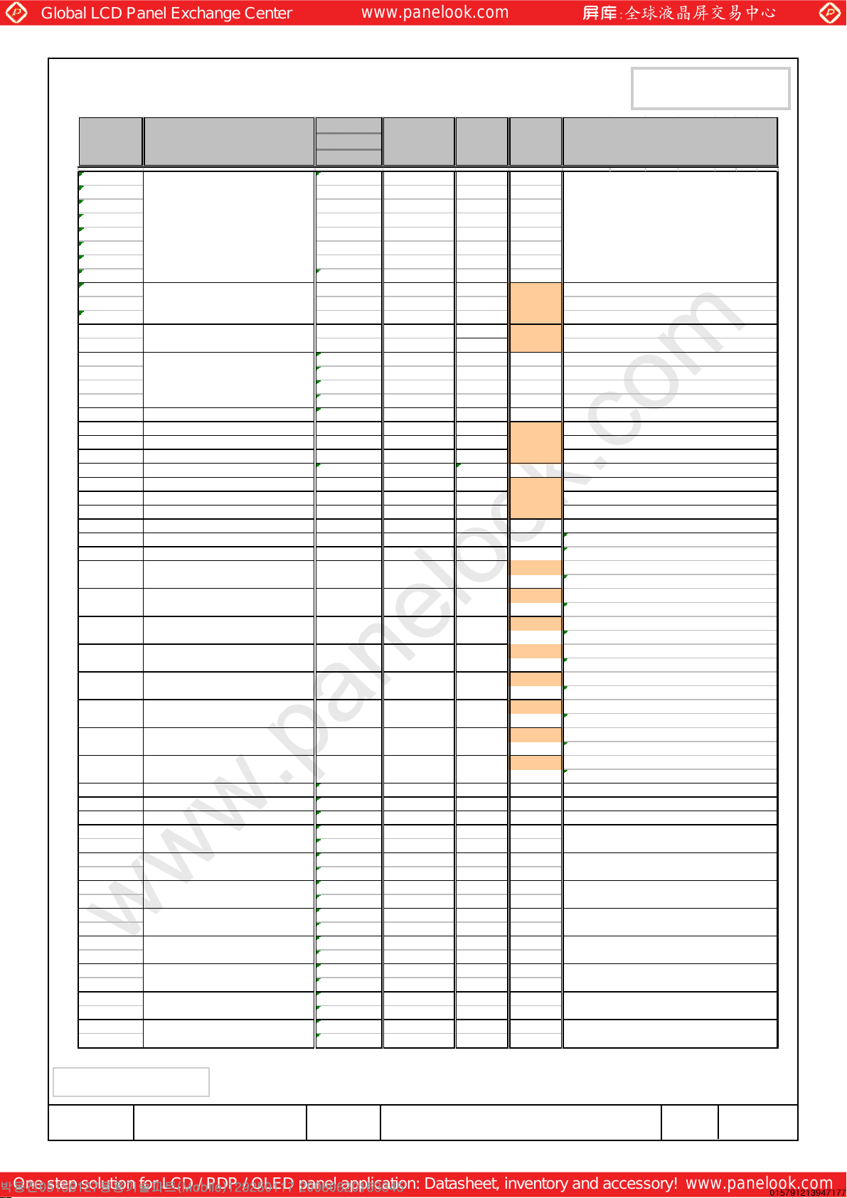
. EDID
ddress Value ASCII
A
FUNCTION BIN
(HEX) HEX Data
00 00 00000000 0
01 FF 11111111 255
02 FF 11111111 255
03 FF 11111111 255
04 FF 11111111 255
05 FF 11111111 255
06 FF 11111111 255
07 00 00000000 0
08 4C 01001100 76 S
09 A3 10100011 163 C
0A 45 01000101
0B 32 00110010
0C 00 00000000 0
0D 00 00000000 0
0E 00 00000000 0
0F 00 00000000 0
10 Week of manufacture 00 00000000 0
11 Year of manufacture 12 00010010 18 2008
12 EDID Structure Ver. 01 00000001 1 1
13 EDID revision # 00 00000000 0 0
14 Video input definition 80 10000000 128
15 Max H im age size 21 00100001 33 33
16 Max V im age size 15 00010101 21 21
17 Display Gamm a 78 01111000 120 2.2
18 Feature support 0A 00001010 10
19 Red/green low bits 87 10000111 135
1A Blue/white low bits F5 11110101 245
1B Red x/ high bits 94 10010100
1C Red y 57 01010111
1D Green x 4F 01001111
1E Green y 8C 10001100
1F Blue x 27 00100111
20 Blue y 27 00100111
21 White x 50 01010000
22 White y 54 01010100
23 Established timing 1 00 00000000 0
24 Established timing 2 00 00000000 0
25 Established timing 3 00 00000000 0
26 01 00000001 1
27 01 00000001 1
28 01 00000001 1
29 01 00000001 1
2A 01 00000001 1
2B 01 00000001 1
2C 01 00000001 1
2D 01 00000001 1
2E 01 00000001 1
2F 01 00000001 1
30 01 00000001 1
31 01 00000001 1
32 01 00000001 1
33 01 00000001 1
34 01 00000001 1
35 01 00000001 1
Header
ID Manufacturer Nam e
ID Product Code
32-bit serial no.
Standard timing #1
Standard timing #2
Standard timing #3
Standard timing #4 not used
Standard timing #5
Standard timing #6
Standard timing #7
Standard timing #8
DEC Notes
69 [E]
50 [2]
148
87
79
140
39
39
80
84
or
E
0.580
0.340
0.310
0.550
0.155
0.155
0.313
0.329
EDID Header
3
character ID
"SEC"
007
2
EDID Ver. 1.0
EDID Rev. 0
33 cm(approx)
21 cm(approx)
Gamm a 2.2
1000010
0
1010101
1
Red x 0.587=
1
0011000
Red y 0.344=
0
1010111
Green x 0.320=
0
1010010
Green y 0.541=
1
0001100
Blue x 0.155=
0100111
0
Blue y 0.130=
0100001
0
White x 0.313=
1010000
0
White y 0.329=
1010100
0
601.088
not used
not used
not used
not used
not used
not used
not used
A
pproval
amsung Secret
S
oc.No. Rev.No
D
0
4-A00-G-080620
Page
31LTN154AT09-8
/
29
Page 30
Global LCD Panel Exchange Center
www.panelook.com
One step solution for LCD / PDP / OLED panel application: Datasheet, inventory and accessory!
www.panelook.com
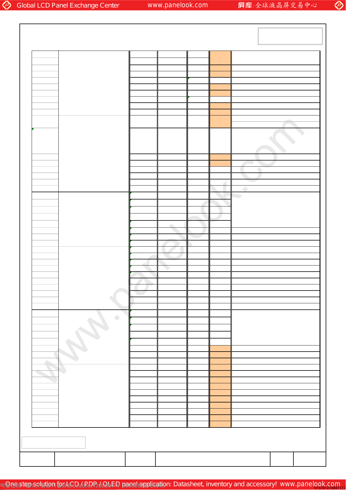
6 8F 10001111 143 70.55
3
37 1B 00011011 27
38 00 00000000 0 1280
39 82 10000010 130 130
3A 50 01010000 80
3B 20 00100000 32 800
3C 22 00100010 34 34
3D 30 00110000 48
3E 10 00010000 16 16
3F 30 00110000 48 48
40
Detailed timing/monitor
descriptor #1
13 00010011 19
A
pproval
Main clock= 68.94 MHz
H
or active=640*2 pixels
Hor blanking=128 pixels
4bit : 4bit
Vertcal active=800 lines
Vertical blanking=16 lines
4bit : 4bit
Hor sync. Offset=16 pixels
H sync. Width=48 pixels
1
3
V sync. Offset=1 lines
V sync. Width=3 lines
1 00 00000000 0
4
42 4B 01001011 75 331
43 CF 11001111 207 207
44 10 00010000 16
45 00 00000000 0
46 00 00000000 0
47 19 00011001 25
48 00 00000000 0
49 00 00000000 0
4A 00 00000000 0
4B 0F 00001111 15
4C 00 00000000 0
4D 00 00000000
4E 00 00000000
4F 00 00000000
50 00 00000000
51 00 00000000
52 00 00000000
53 00 00000000
54 00 00000000
55 23 00100011
56 87 10000111
57 02 00000010
58 64 01100100
59 01 00000001
5A 00 00000000 0
5B 00 00000000 0
5C 00 00000000 0
5D FE 11111110 254
5E 00 00000000 0
5F 53 01010011 83 [S]
60 41 01000001 65 [A]
61 4D 01001101 77 [M]
62 53 01010011 83 [S]
63 55 01010101 85 [U]
64 4E 01001110 78 [N]
65 47 01000111 71 [G]
66 0A 00001010 10 [^]
67 20 00100000 32 [ ]
68 20 00100000 32 [ ]
69 20 00100000 32 [ ]
6A 20 00100000 32 [ ]
6B 20 00100000 32 [ ]
Detailed timing/monitor
descriptor #2
Detailed timing/monitor
descriptor #3
0
0
0
0
0
0
0
0
35
135
2
100
1
bit : 2bit :2bit :2bit
2
H
image size= 331 mm(approx)
V image size = 207 mm(approx)
No Horizontal Border
No Vertical Border
Manufacturer Specified (Timing)
=HSPWmin / 2
Value
=HSPWmax / 2
Value
=Thbpmin /2
Value
=Thbpmax /2
Value
=VSPWmin /2
Value
=VSPWmax /2
Value
=Tvbpmin / 2
alue
V
=Tvbpmax / 2
Value
Thpmin=
Thpmax=
Tvpmin=
Tvpmax=
M
odule revision
SCII Data String Tag
A
*2 + HA pixelclks
value
*2 + HA pixelclks
value
*2 + VA lines
value
*2 + VA lines
value
amsung Secret
S
oc.No. Rev.No
D
0
4-A00-G-080620
Page
31LTN154AT09-8
/
30
Page 31
Global LCD Panel Exchange Center
www.panelook.com
One step solution for LCD / PDP / OLED panel application: Datasheet, inventory and accessory!
www.panelook.com
C 00 00000000 0
6
6D 00 00000000 0
6E 00 00000000 0
6F FE 11111110 254
70 00 00000000 0
71 4C 01001100 76 [L]
72 54 01010100 84 [T]
73 4E 01001110 78 [N]
74 31 00110001 49 [1]
75 35 00110101 53 [5]
76 34 00110100 52 [4]
77 41 01000001 65 [A]
78 54 01010100 84 [T]
79 30 00110000 48 [0]
7A 39 00111001 57 [9]
7B 30 00110000 48 [0]
7C 30 00110000 48 [0]
7D 30 00110000 48 [0]
7E Extension Flag 00 00000000 0
7F Checksum
Detailed timing/monitor
descriptor #4
93
10010011
147
A
pproval
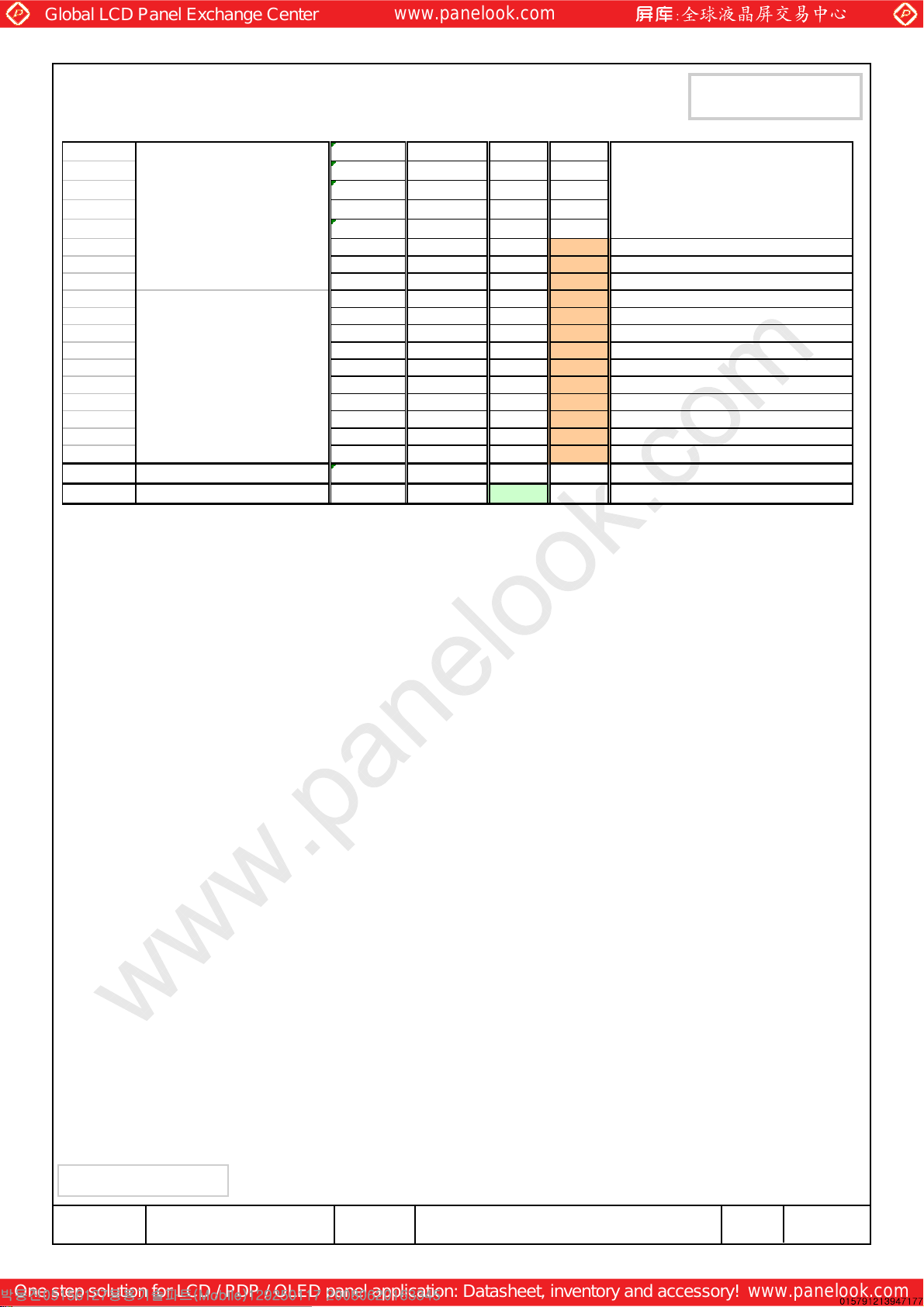
Monitor Name Tag (ASCII)
amsung Secret
S
oc.No. Rev.No
D
0
4-A00-G-080620
Page
31LTN154AT09-8
/
31
 Loading...