

Page 1
Product Information
Samsung Electronics Co
Ltd
TO
DATE
: General
: Jan. 25 , 2013
SAMSUNG TFT-LCD
MODEL NO. : LTN156AT19-0
NOTE : Extension code [ - 0xx ]
→ LTN156AT19-0xx
Surface type [ A/G ]
Any modification of Spec is not allowed without SEC’s permission
Application engineering part, Mobile Division
.,
.
Samsung Secret
Doc.No. Rev.No
04-A00-G-130125
Page
/ 31LTN156AT19-0
1
Page 2
CONTENTS
5.2 LVDS Interface
6.2 Timi
Product Information
Revision History -------------------( 3 )
General Description
1. Absolute Maximum Ratings
1.1 Absolute Ratings of environment
1.2 Electrical Absolute Ratings
2. Optical Characteristics
3. Electrical Characteristics
3.1 TFT LCD Module
3.2 Backlight Unit
3.3 LED Driver
4. Block Diagram
4.1 TFT LCD Module
4.2 LED Placement Structure
5. Input Terminal Pin Assignment
5.1 Input Signal & Power
5.3 Timing Diagrams of LVDS For Transmitting
5.4 Pixel format
-------------------( 4 )
-------------------( 5 )
-------------------( 7 )
-------------------( 10 )
-------------------( 13 )
-------------------( 14 )
6. Interface Timing
6.1 Timing Parameters
6.3 Power ON/OFF Sequence
7. Outline Dimension
8. Packing
9. Markings & Others
10. General Precautions
11. EDID
Samsung Secret
-------------------( 19 )
ng Diagrams of interface Signal
-------------------( 222 )
-------------------( 24 )
-------------------( 25 )
-------------------( 27 )
------------- ------( 29 )
Doc.No. Rev.No
04-A00-G-130125
Page
/ 31LTN156AT19-0
2
Page 3
REVISION HISTORY
A00A
Product Information
Date Revision No. Page
Jan, 25. 2013
Summary
ll The approval specification of 15.6” SMS HD was issued first.
CODE REVISION HISTORY
Date Model. Revision No. Summary
June, 15. 2011 LTN156AT19 001 Basic model
Samsung Secret
Doc.No. Rev.No
04-A00-G-130125
Page
/ 31LTN156AT19-0
3
Page 4
Product Information
LTN156AT19 is a color active matrix TFT (Thin Film Transistor) liquid crystal display
LVDS Interf
Number of pixel
1366 * 768
pixel
GENERAL DESCRIPTION
DESCRIPTION
(LCD) that uses amorphous silicon TFT as switching devices.
This model is composed of a TFT LCD panel, a driver circuit and a backlight unit.
The resolution of a 15.6” contains 1366 x 768 pixels and can display up to 262,144colors.
6 O'clock direction is the optimum viewing angle.
FEATURES
• High contrast ratio
• HD(1366 x 768 pixels ) resolution
• Fast Response
• LED Back Light with embedded LED Driver
• DE (Data enable) only mode
•3.3V
• Onboard EEDID chip
ace
APPLICATIONS
•Notebook PC
• If the usage of this product is not for PC application, but for others, please contact SEC
GENERAL INFORMATION
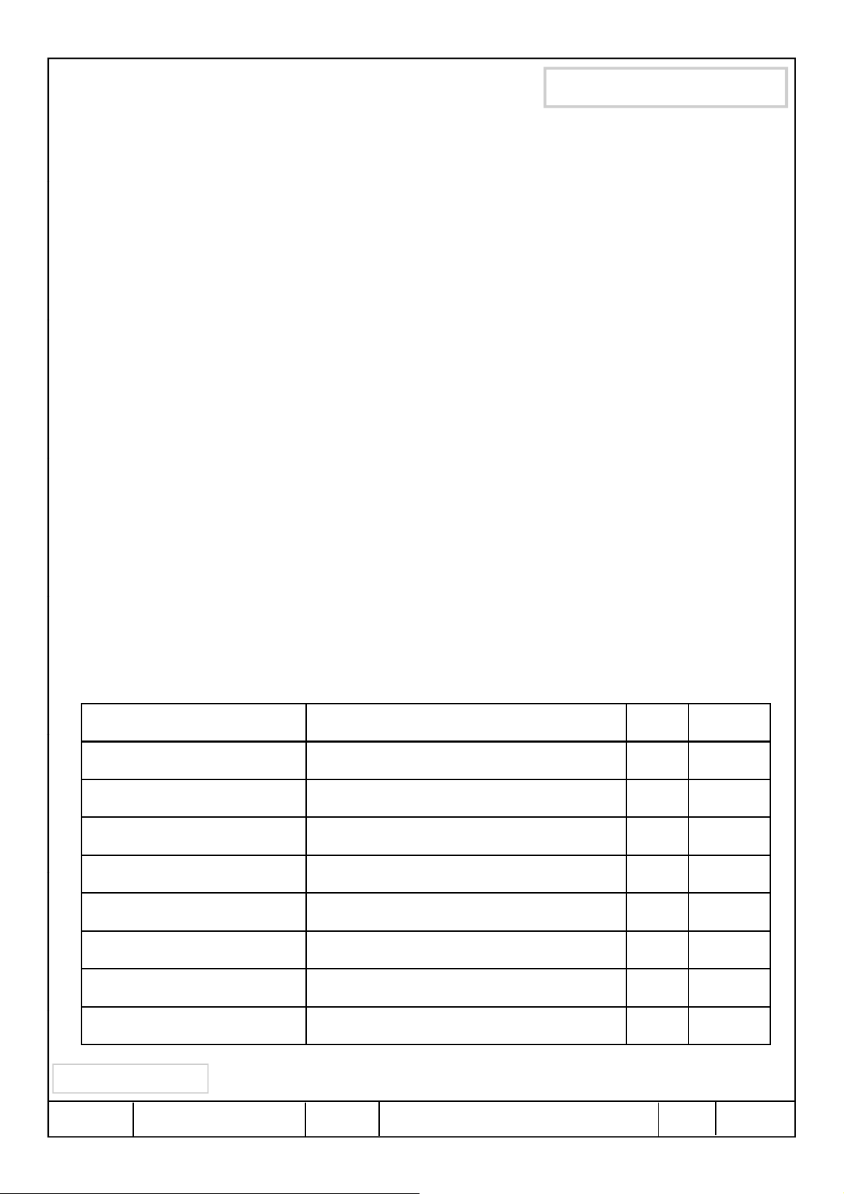
Item Specification Unit Note
Display area 344.232 (H) x 193.536 (V) (15.6”diagonal)
Driver element
Display colors
Pixel arrangement
Pixel pitch 0.252 (H) x 0.252 (V) (TYP.)
a-Si TFT active matrix
262,144
RGB vertical stripe
mm
mm
Display Mode
Surface treatment
Samsung Secret
Doc.No. Rev.No
Normally white
Haze 25%, Hardness 2H
04-A00-G-130125
Page
A/G
/ 31LTN156AT19-0
4
Page 5
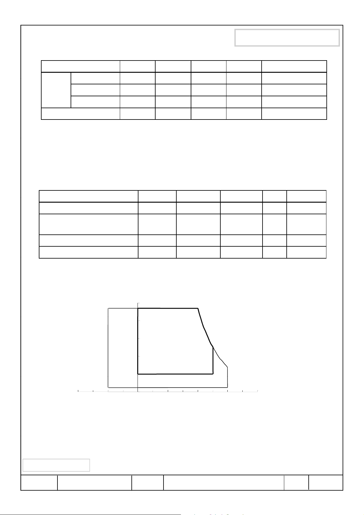
Mechanical Information
Horizontal (H)
358.8
359.3
359.8
mm
f (mini
)
Item
Symbol
Min.
Max.
Unit
Note
(3) 5
500 Hz, random vibration, 30min for X, Y, Z
Item Min. Typ. Max. Unit Note
Product Information
Module
size
Note (1) Measurement condition of outline dimension
Vertical (V) 209.0 209.5 210.0 mm
Depth (D) - - 4.0 mm
Weight - - 430 g
. Equipment : Bernier Calipers
. Push Force : 500g
1. ABSOLUTE MAXIMUM RATINGS
1.1 ENVIRONMENTAL ABSOLUTE RATINGS
Storage temperate TSTG -20 60
Operating temperate
(Temperature of glass surface)
Shock ( non-operating ) Snop - 240 G (2),(4)
Vibration (non-operating) Vnop - 2.41 G (3),(4)
TOPR 0 50
mum
C
C
(1)
(1)
Note (1) Temperature and relative humidity range are shown in the figure below.
95 % RH Max. (40 C Ta)
Maximum wet - bulb temperature at 39
100
Relative Humidity ( %RH)
90
80
60
40
20
Operating Range
O
C or less. (Ta 40 C ) No condensation
( 40,90 )
( 50,50.4 )
( 60,27.7 )
Storage Range
5
0
-40 -20 0 20 40 60 80
Temperature (OC)
(2) 2ms, half sine wave, one time for X, Y, Z.
-
(4) At testing Vibration and Shock, the fixture in holding the Module to be tested have to be
hard and rigid enough so that the Module would not be twisted or bent by the fixture.
.
Samsung Secret
Doc.No. Rev.No
04-A00-G-130125
Page
/ 31LTN156AT19-0
5
Page 6
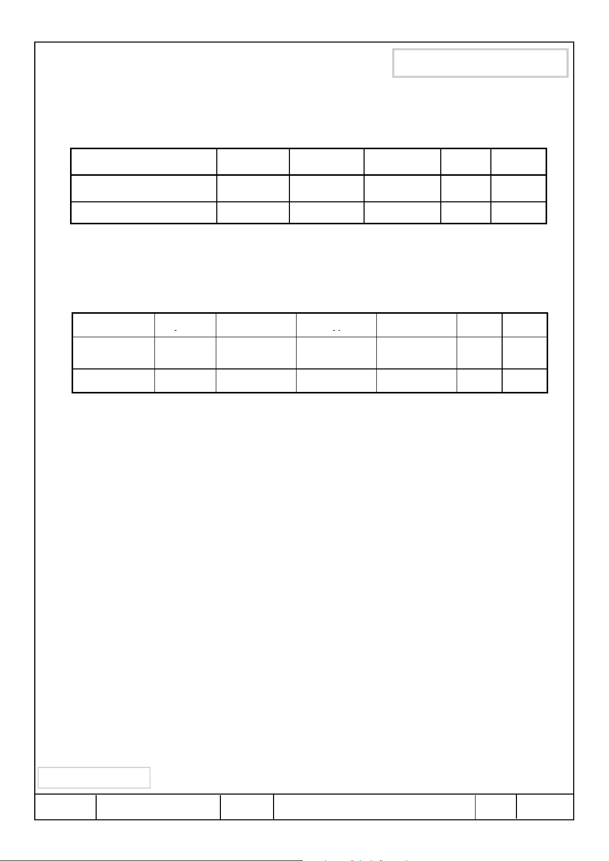
1.2 ELECTRICAL ABSOLUTE RATINGS
y
yp
(1) TFT LCD MODULE
Item Symbol Min. Max. Unit Note
Product Information
VDD =3.3V, VSS = GND = 0V
Power Supply Voltage V
Logic Input Voltage V
Note (1) Within Ta (25 2 C)
DD VDD -0.3 VDD + 0.3 V (1)
IN VDD -0.3 VDD + 0.3 V (1)
(2) BACK-LIGHT UNIT
Item Symbol Min. Typ. Max. Unit Note
LED Current IL -22-
LED Voltage V
Note 1) Permanent damage to the device may occur if maximum values are exceeded
Functional operation should be restricted to the conditions described under normal operating conditions.
L -3.2-V(1)
Ta = 25 2 C
mArm
s
(1)
Samsung Secret
Doc.No. Rev.No
04-A00-G-130125
Page
/ 31LTN156AT19-0
6
Page 7
Product Information
ith th
(5)
IF=100%
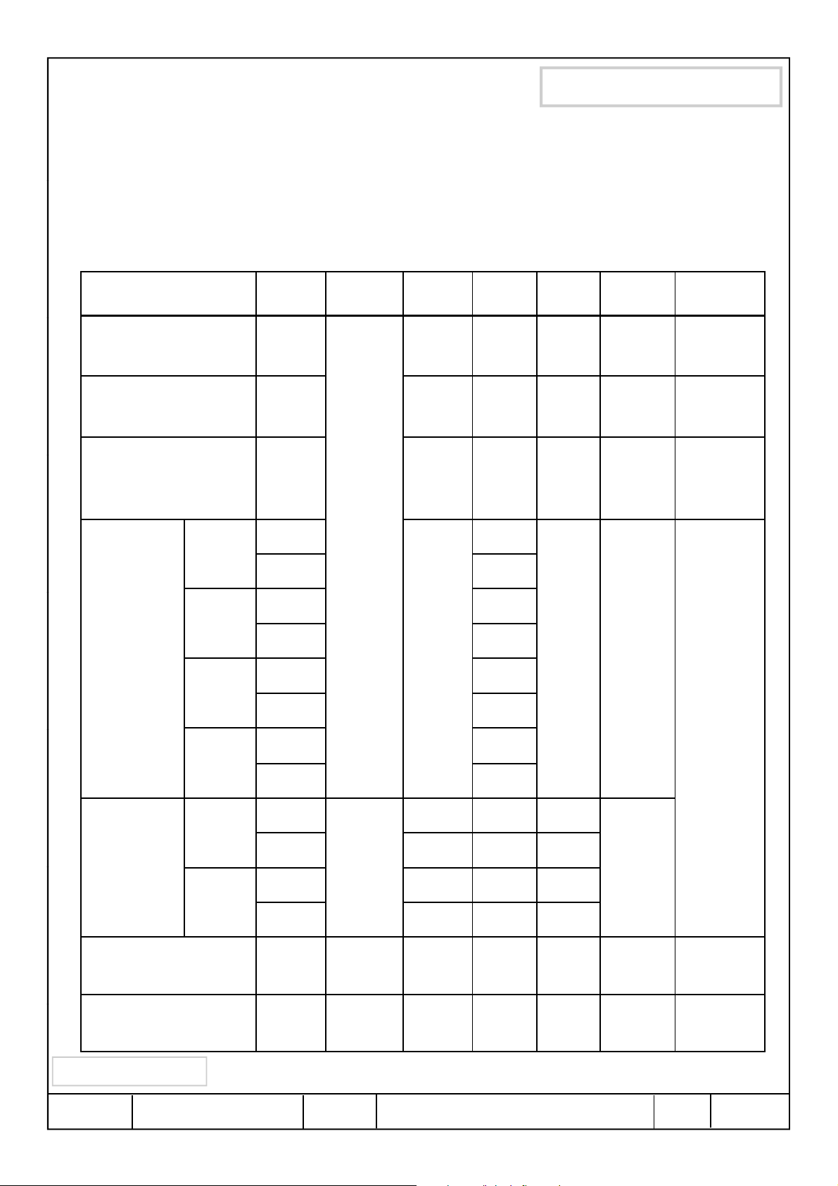
2. OPTICAL CHARACTERISTICS
The following items are measured under stable conditions. The optical characteristics
should be measured in a dark room or equivalent state w
Measuring equipment : TOPCON SR-3
e methods shown in Note
.
Item Symbol
Contrast Ratio
(5 Points)
Response Time at Ta
( Rising + Falling )
Average Luminance
of White (5 Points)
Red
Green
Color
Chromaticity
( CIE )
Blue
White
* Ta = 25 2 C, V
Conditio
n
=3.3V, fv= 60Hz, fDCLK = 70.7MHz, IF = 100% duty
DD
Min. Typ. Max Unit Note
CR 300 - - - (1), (2), (5)
T
RT -1625msec(1), (3)
Y
L,AVE 200 220 - cd/m
2
duty
(1), (4)
Normal
X 0.570
R
Viewing
Angle
Y 0.340
R
G
X 0.330
Y 0.560
G
X 0.160
B
Y 0.135
B
X 0.313
W
Y 0.329
W
= 0
= 0
Typ-
0.03
Typ
+0.03
-
(1), (5)
SR-3
L
Hor.
Viewing
Angle At center
Ver.
H
H
L
CR 10
Color Gamut CG - 45 - %
13 Points
White Variation
L
Samsung Secret
Doc.No. Rev.No
40 45 -
40 45 -
Degrees
15 15 -
30 30- -
--2.0- (6)
04-A00-G-130125
Page
/ 31LTN156AT19-0
7
Page 8
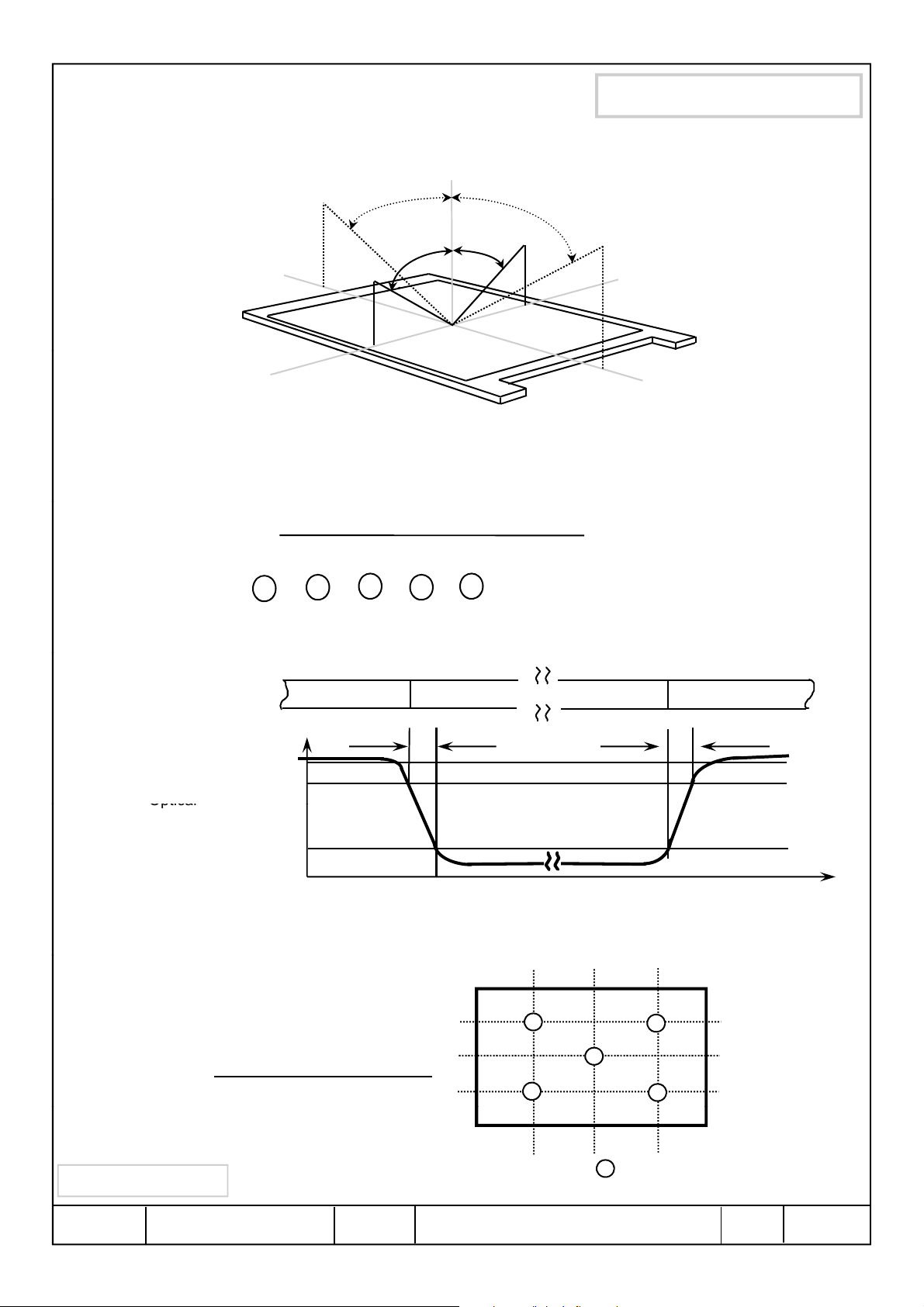
Note 1) Definition of Viewing Angle : Viewing angle range(10 C/R)
Optical
(li
)
Normal Line
o
= 0
L
, = 0
o
R
L
L
=90
o
xy
H
Product Information
12 O’clock
direction
H= 90
o
6 O’clock
direction
L= 90
o
x'y'
R=90
Note 2) Definition of Contrast Ratio (CR) : Ratio of gray max (Gmax) ,gray min (Gmin)
at 5 points(4, 5, 7, 9, 10)
CR(4) + CR(5) + CR(7) + CR(9) + CR(10)
CR =
5
Points : , , , , at the figure of Note (6).
4 9
5
7
10
Note 3) Definition of Response time :
Display data
White(TFT OFF) White(TFT OFF)
TR
Black(TFT ON)
TF
100%
90%
Response
10%
0%
o
Note 4) Definition of Average Luminance of White : measure the luminance of white at 5 points.
Average Luminance of White ( YL,AVE )
Y
L4 + YL5 + YL7 + YL9 + YL10
YL,AVE =
5
Samsung Secret
Doc.No. Rev.No
25% 50% 75%
10
7
5
04-A00-G-130125
9
4
: test point
Time
VIEW AREA
25%
50%
75%
nes
Page
8
/ 31LTN156AT19-0
Page 9
Product Information
A
Minimum luminance of 13 points
231
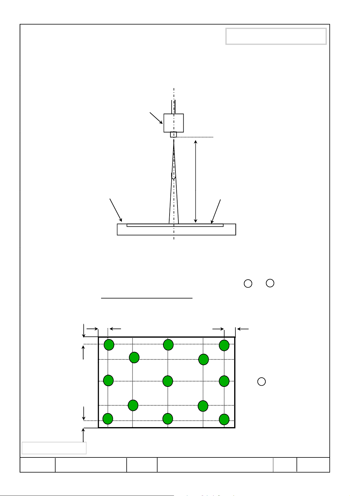
Note 5) After stabilizing and leaving the panel alone at a given temperature for 30 min , the measurement
should be executed. Measurement should be executed in a stable, windless,and dark room.
30 min after lighting the backlight. This should be measured in the center of screen.
IF current : 22m
Environment condition : Ta = 25 2 C
Photo-detector
( TOPCON SR-3 )
Field
= 2
50 cm
TFT-LCD module
Center of the screen
[ Optical characteristics measurement setup ]
Note 6) Definition of 13 points white variation ( L ), CR variation( CVER ) [ ~ ]
Maximum luminance of 13 points
LCD panel
113
L =
10mm
11
25%
10mm
10mm
13 12
25% 50% 75%
10
9
10mm
Samsung Secret
Doc.No. Rev.No
8
5
7
4
04-A00-G-130125
6
50%
75%
(lines)
: test point
Page
/ 31LTN156AT19-0
9
Page 10
3. ELECTRICAL CHARACTERISTICS
y
yp
(2)
()
,,,
Product Information
3.1 TFT LCD MODULE
Item Symbol Min. Typ. Max. Unit Note
Voltage of Power Supply VDD 3.0 3.3 3.6 V
Differential Input
Voltage for LVDS
Receiver Threshold
Vsync Frequency fv - 60 - Hz
Main Frequency f
Rush Current I
Current of Power
Supply
High V
Low V
IH - - +100 mV VCM = +1.2V
IL -100 - - mV
DCLK 66.14 70.7 83.88 MHz -
RUSH --1.5A (4)
White - 230 - mA
Mosaic - 230 - mA
IDD
V.stripe - 300 350 mA
Ta= 25 2C
*a),b),c)
Note (1) Display data pins and timing signal pins should be connected.( GND = 0V )
fV = 60Hz, fDCLK = 72.33MHZ, VDD = 3.3V , DC Current.
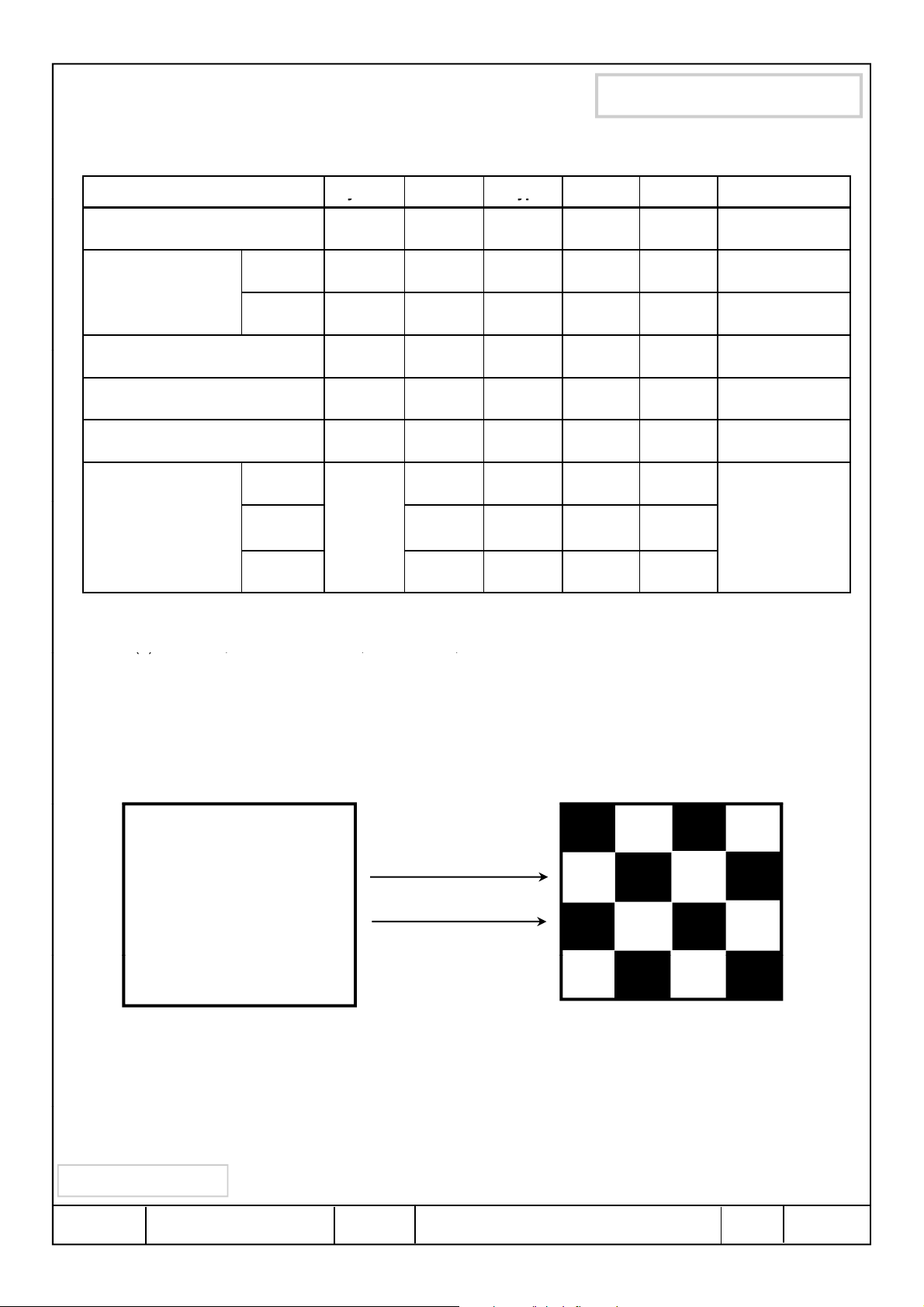
(3) Power dissipation pattern
*a) White Pattern *b) Mosaic Pattern
VIEW AREA
Display Brightest Gray Level
Display Darkest Gray Level
Samsung Secret
Doc.No. Rev.No
04-A00-G-130125
Page
10
/ 31LTN156AT19-0
Page 11
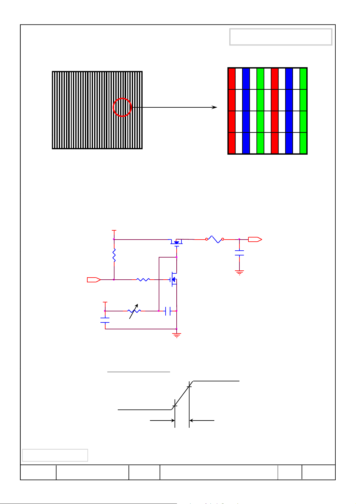
*c) 1dot Vertical stripe pattern
RGBRGBRGBRG
R1
C1
VDDrising time is 470us
4) Rush current measurement condition
Product Information
GBRGB RGBRG
R
GBRGB RGBRG
R
RGBRGBRGBRG
CONTROL SIGNAL
(HIGH to LOW)
12V
3.3V
C3
1uF
47K
47K
R2
1K
M1
2SK1059
C2R3
10000pF
0.9VDD
VDD ( LCD INPUT)
FUSE
1uF
M2
2SK1399
3.3V
Samsung Secret
Doc.No. Rev.No
GND
0.1VDD
470us
04-A00-G-130125
Page
11
/ 31LTN156AT19-0
Page 12
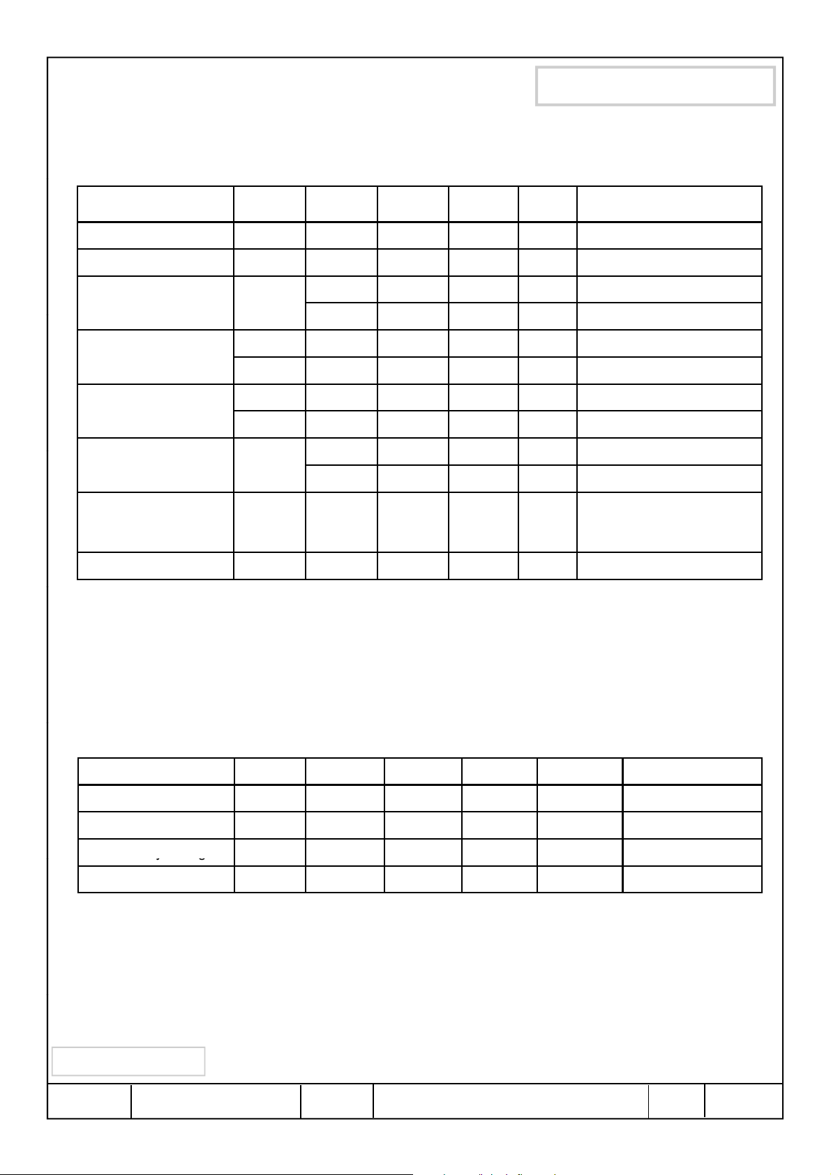
3.2 LED Driver
3.3
3.5W@ Max
5-100%PWM freq : 200Hz~10KHz
y
yg
Product Information
- On board LED Driver (Intersil)
Item- Symbol Min. Typ. Max. Unit Note
Input Voltage V
Input Current I - 270 - mA -
power consumption P
EN control level
PWM control level
PWM Control Duty
Ratio
External PWM
Dimming Control
Frequency (BLIM)
Operating Life Time Hr 10,000 - - Hour
in 71220V -
- 0.9 1.0 W @ 60nit
-
ON 2.0 - - V
OFF - - 0.8 V
ON 2.0 - - V
OFF - - 0.8 V
D
F
BLIM 0.2 1 10 kHz
10 - 100 PWM freq : 1KHz~10KHz
Ta= 25 2 C
Note (1) Life time (Hr) of LEDs can be defined as the time in which it continues to operate under the
condition Ta= 25 2 C and IF = 22mA
When the brightness becomes 50% or lower than the original.
rms until one of the following event occurs.
3.3 BACK-LIGHT UNIT
Ta= 25 2 C
Item Symbol Min. Typ. Max. Unit Note
LED Forward Current IF - 22 - mA
LED Forward Voltage VF 3.0 3.2 3.4 V
LED Arra
BL consumption P - - 3.3 W @ MAX
VoltageVP - 36 - V
Samsung Secret
Doc.No. Rev.No
04-A00-G-130125
Page
12
/ 31LTN156AT19-0
Page 13
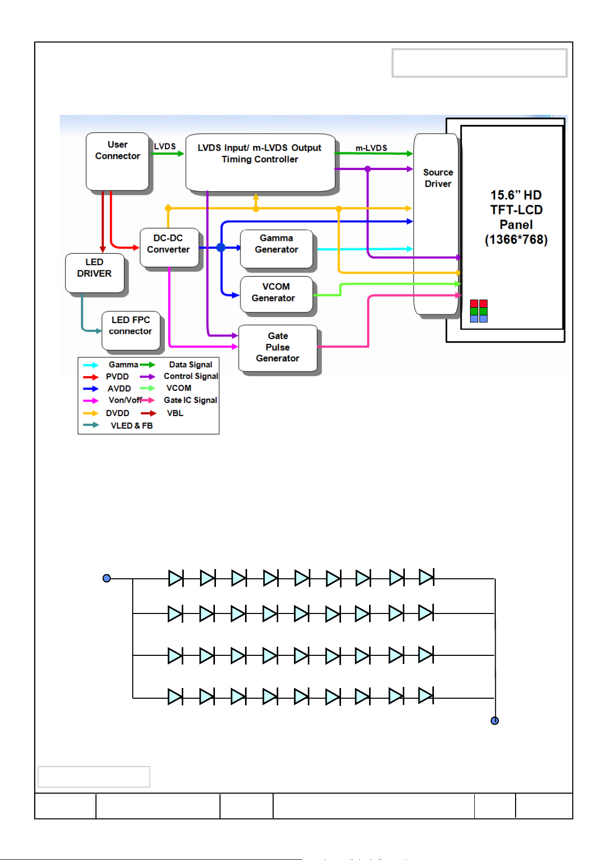
4. BLOCK DIAGRAM
4.1 TFT LCD Module
Product Information
4.2 LED placement structure
D1 D2 D3 D4 D5 D6
Anode
Samsung Secret
Doc.No. Rev.No
D7
D8
04-A00-G-130125
D9
Page
Cathode
/ 31LTN156AT19-0
13
Page 14
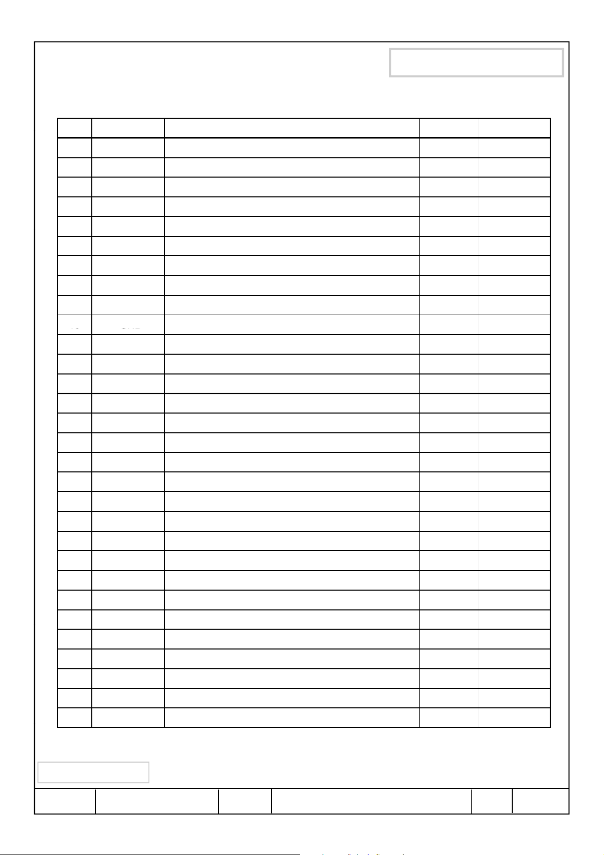
5. INPUT TERMINAL PIN ASSIGNMENT
No.
Symbol
Function
Polarity
Remarks
5NCNo Connection
10
GND
Ground
+LVDS differential data input (B2
B5, HS, VS, DE)
Product Information
5.1. Input Signal & Power (LVDS, Connector : I-PEX 20455-#40E-## or equivalent )
1 NC No Connection (Reserved for supplier)
2 AVDD
3 AVDD
4DVDD
6SCL
7SDA
8RIN0-
9RIN0+
11 RIN1-
12 RIN1+
13 GND
14 RIN2- -LVDS differential data input (B2-B5, HS, VS, DE)
15 RIN2+
16 GND
Power Supply 3.3V (typical)
Power Supply 3.3V (typical)
DDC 3.3V power
DDC Clock
DDC data
-LVDS differential data input (R0-R5, G0)
+LVDS differential data input (R0-R5, G0)
-LVDS differential data input (G1-G5, B0-B1)
+LVDS differential data input (G1-G5, B0-B1)
Ground
-
Ground
Negative
Positive
Negative
Positive
Negative
Positive
17 CLK- -LVDS differential clock input
18 CLK+ +LVDS differential clock input
19 GND Ground
20 NC No connection
21 NC No connection
22 GND Ground
23 NC No connection
24 NC No connection
25 GND Ground
26 NC No connection
27 NC No connection
28 GND Ground
29 NC No Connect
30 NC No Connect
Negative
Positive
Samsung Secret
Doc.No. Rev.No
04-A00-G-130125
Page
14
/ 31LTN156AT19-0
Page 15
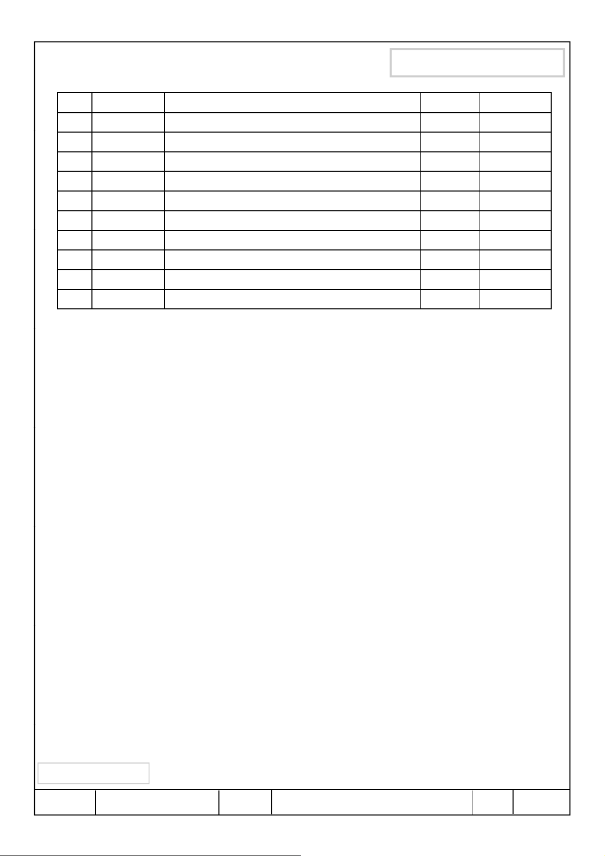
Product Information
No. Symbol Function Polarity Remarks
31 VSSLED Ground – LED
32 VSSLED Ground – LED
33 VSSLED Ground – LED
34 NC No Connect
35 PWM System PWM Signal Input (+3.3V Swing)
36 LED_EN LED enable pin (+3.3V Input)
37 NC No Connect
38 VDDLED LED power
39 VDDLED LED power
40 VDDLED LED power
Samsung Secret
Doc.No. Rev.No
04-A00-G-130125
Page
15
/ 31LTN156AT19-0
Page 16
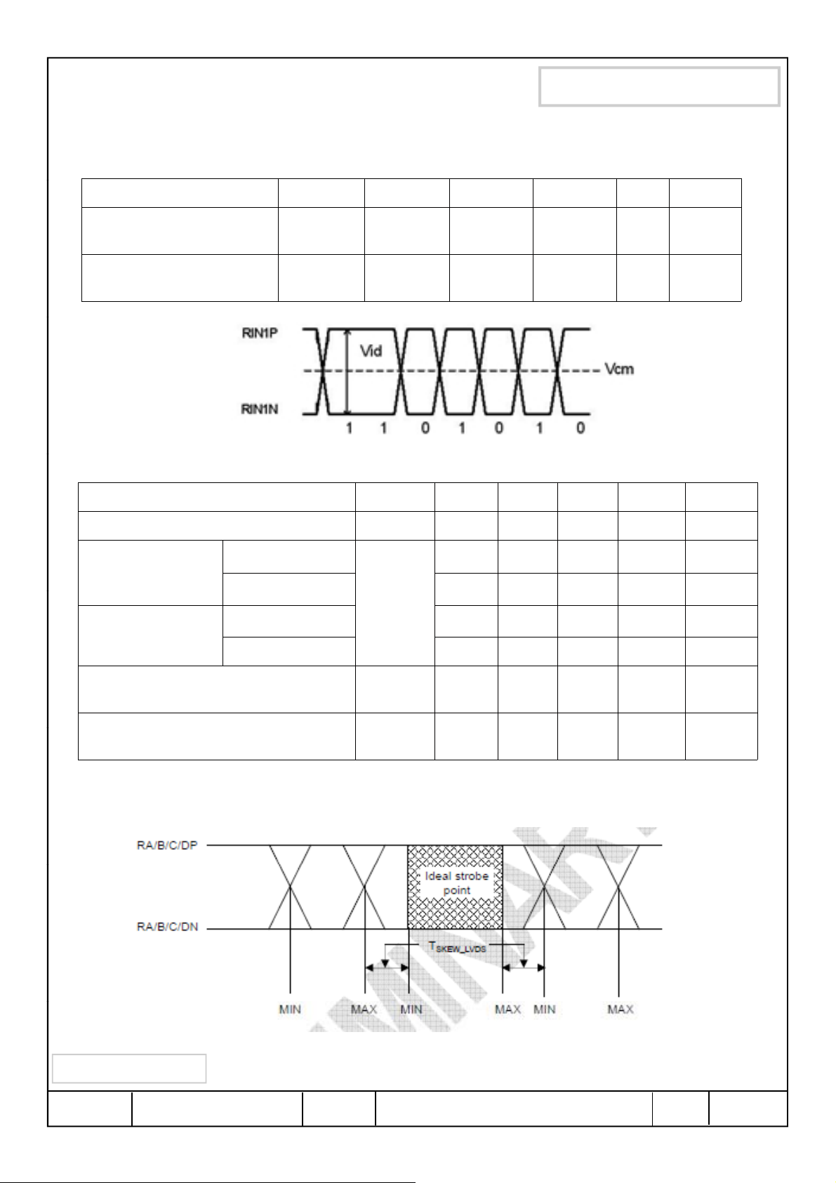
5.2 LVDS Interface
5.2.1 LVDS AC I
t
50MHz
700ps(1),(2)
Modulating frequency of LVDS
5.2.1 LVDS DC Input
ITEM SYMBOL MIN. TYP. MAX. UNIT NOTE
Product Information
LVDS Differential
Voltage
Input Common Mode
Voltage
VID
V
CM
npu
ITEM SYMBOL MIN. TYP. MAX. UNIT NOTE
LVDS input Clock Frequency F
LVDS RX skew
Right margin
LVDS RX skew
Left margin
100MHz - - 270 ps (1),(2)
100MHz -270 - - ps (1),(2)
50MHz -700 - - ps (1),(2)
200 - 600
0.4 1.2 1.7 V
CLK_LVDS
30 100 Mhz
--
T
RSRM
mV
Maximum deviation of LVDS input
clock during SSCG
input clock during SSCG
F
F
CLK_MOD
Note (1) : LVDS Receiver Skew (Strobe) Margin
Samsung Secret
CLK_DEV
- - ± 3 % (3)
30 - 300 KHz (3)
Doc.No. Rev.No
04-A00-G-130125
Page
16
/ 31LTN156AT19-0
Page 17
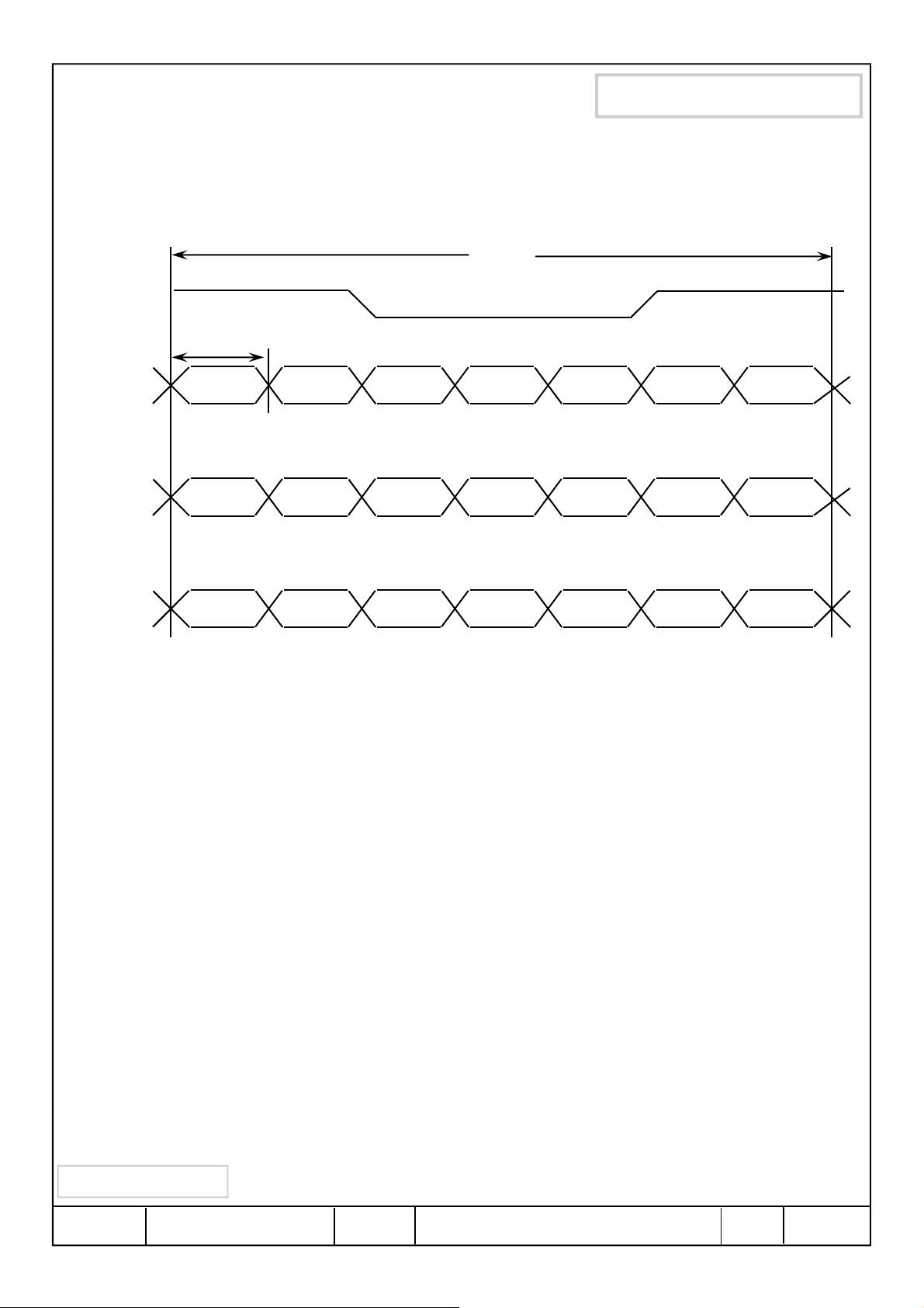
5.3 Timing Diagrams of LVDS For Transmission
T/7
RxOUT13
RxOUT12
RxOUT10
RxOUT11
RxOUT9
RxOUT8
RxOUT7
Rx IN1
G0R4R5R2R1R0R3
LVDS Receiver : Integrated T-con
TxCLK OUT
RxCLK IN
Product Information
T
Rx IN2
RxIN0
RxOUT20 RxOUT19 RxOUT17RxOUT18 RxOUT16 RxOUT15 RxOUT14
DE
RxOUT6 RxOUT5 RxOUT3RxOUT4 RxOUT2 RxOUT1 RxOUT0
Vsync B2Hsync B5 B3B4
G4B1 G5B0 G3 G2 G1
Samsung Secret
Doc.No. Rev.No
04-A00-G-130125
Page
17
/ 31LTN156AT19-0
Page 18
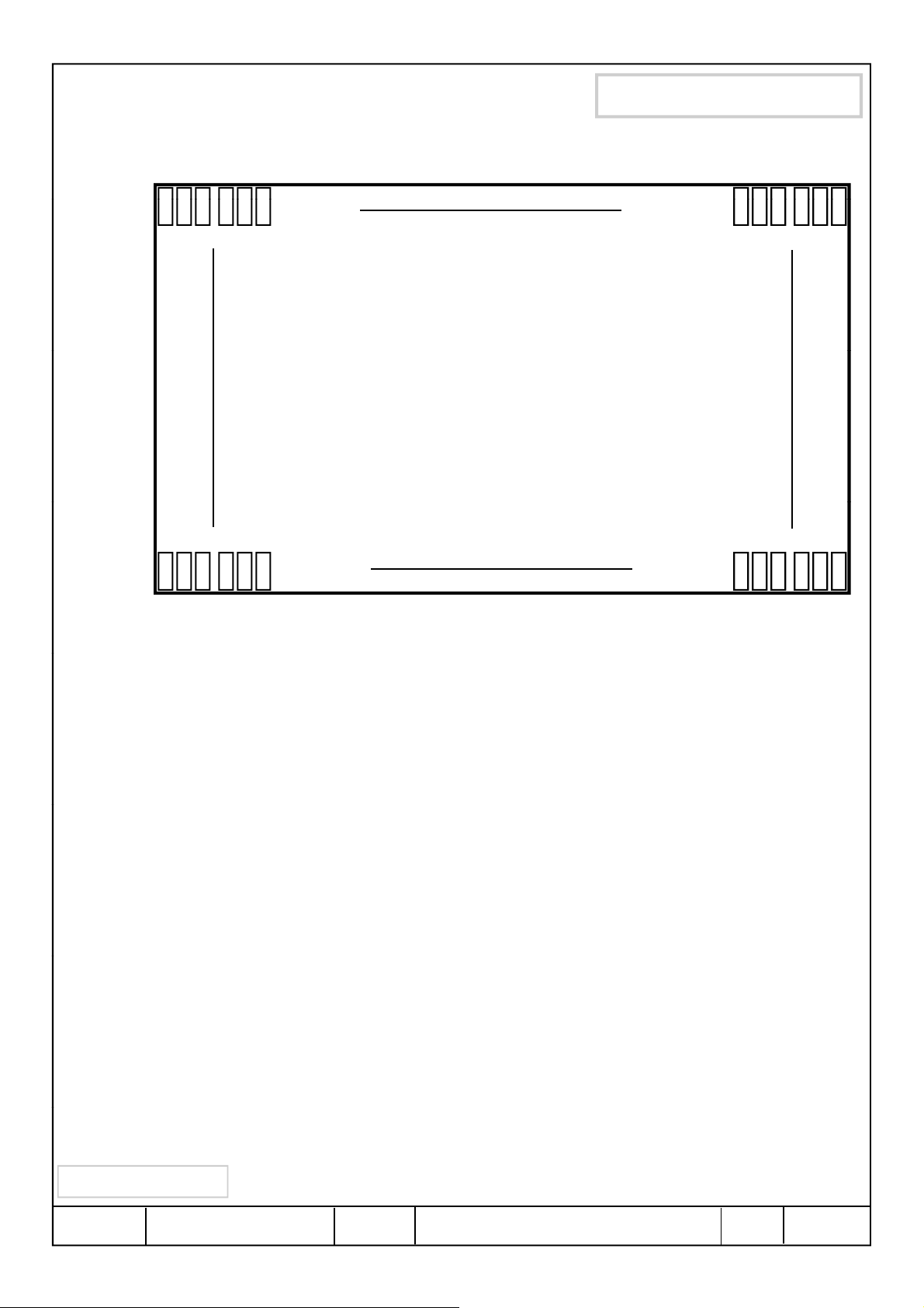
5.4 Pixel Format in the display
Product Information
Line 1
Line 768
1
RGB RGB RGB RGB
1366
LTN156AT19Panel
RGB RGB RGB RGB
Samsung Secret
Doc.No. Rev.No
04-A00-G-130125
Page
18
/ 31LTN156AT19-0
Page 19
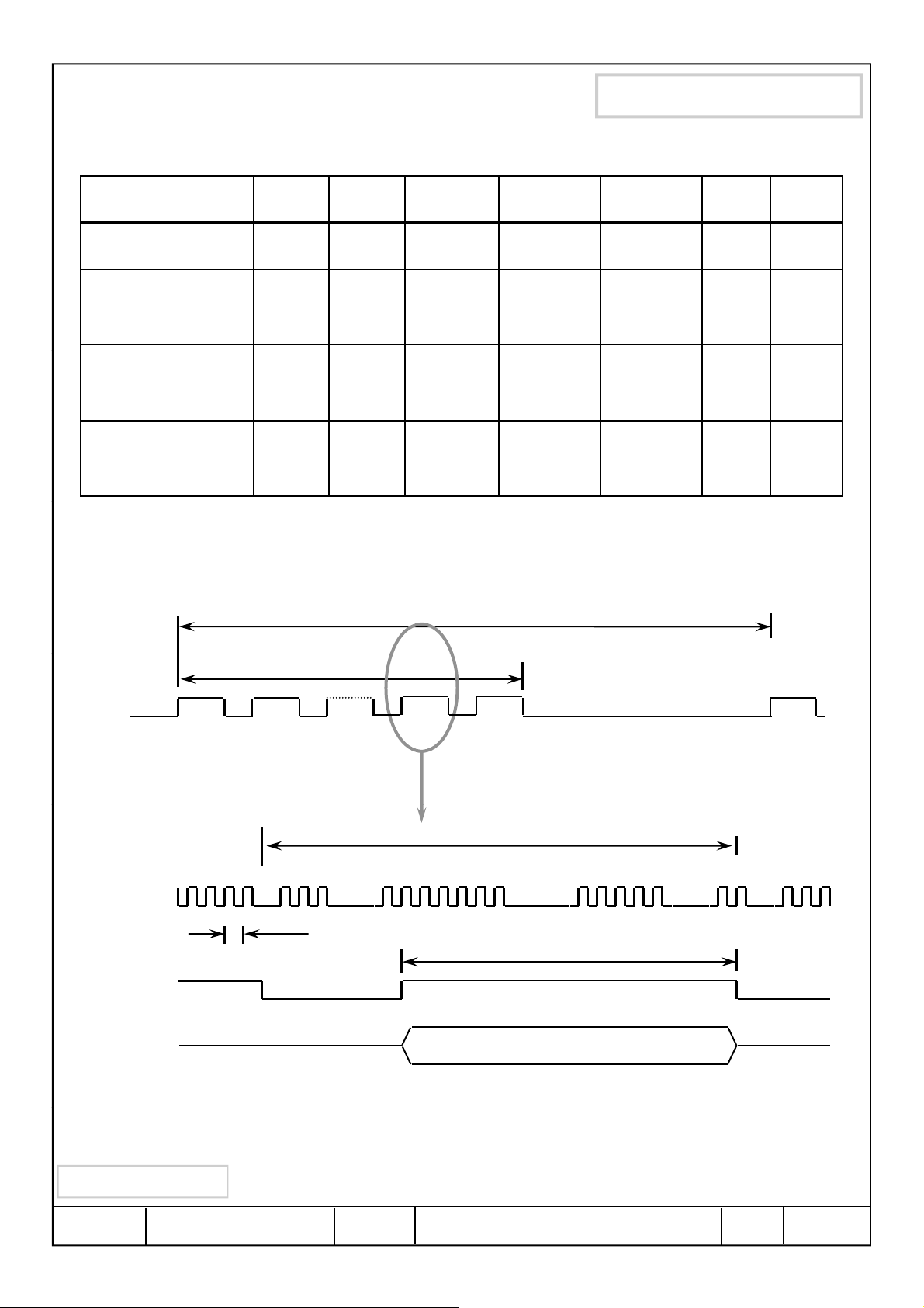
6. INTERFACE TIMING
Signal
Item
Symbol
Min.Typ.Max.Unit
Note
Product Information
6.1 Timing Parameters
Frame Frequency Cycle TV 773 790 810 Lines
Vertical Active
Display Term
One Line
Scanning Time
Horizontal Active
Display Term
Display
Period
Cycle TH 1426 1526 1726 Clocks
Display
Period
TVD - 768 - Lines
THD - 1366 - Clocks
6.2 Timing diagrams of interface signal
TVD
DE
TV
DCLK
TC
DE
DATA
SIGNALS
Samsung Secret
Doc.No. Rev.No
TH
THD
Valid display data ( 1366 clocks)
04-A00-G-130125
Page
19
/ 31LTN156AT19-0
Page 20
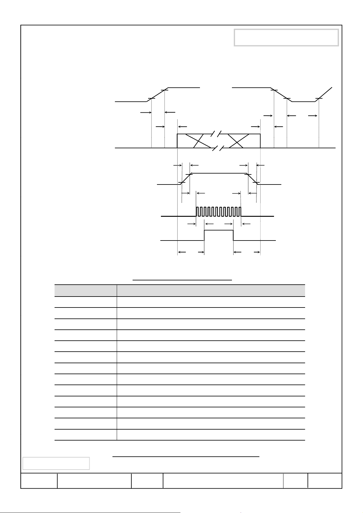
6.3 Power ON/OFF Sequence
0 ≤T13
Delay from B/L Enable Off to PWM Off
Product Information
: To prevent a latch-up or DC operation of the LCD module, the power on/off sequence
should be as the diagram below.
Power Supply VDD
0V
Signals
LED Power (V
)
in
PWM for LED driver
(Dimming signal)
Enable signal for LED driver
(Backlight on/off)
0.1 V
0 V
0.9 V
DD
0.1 LED V
DD
T1
T2
0.9 LED V
0.9 V
DD
0.1 V
DD
T7
T3
VALID
T8
in
in
T10
T12
T5
T9
T11
T13
T6
0.9 LED V
0.1 LED V
in
T4
in
Timing (ms) Remarks
0.5<T1≤10
0<T2 ≤50
0<T3 ≤50
500 ≤T4
300 ≤T5
200 ≤T6
0<T7 ≤10
0.5<T8≤10
0.5<T9≤10
0 ≤T10
0≤T11
0≤T12
Samsung Secret
Power ON/OFF Sequence
rising time from 10% to 90%
V
DD
Delay from V
Delay from valid data OFF to V
V
OFF time for Windows restart
DD
Delay from valid data to B/L enable at power ON
Delay from valid data off to B/L disable at power Off
V
falling time from 90% to 10%
DD
LED V
LED V
Delay from LED driver Vin rising time 90% to PWM ON
Delay from PWM Off to LED driver Vin falling time 10%, Must Keep rule
Delay from PWM ON to B/L Enable ON, Must Keep rule
rising time from 10% to 90%
in
falling time from 90% to 10%
in
to valid data at power ON
DD
OFF at power Off
DD
Power Sequence & Timing Parameters
Doc.No. Rev.No
04-A00-G-130125
Page
20
/ 31LTN156AT19-0
Page 21
6.3 Power ON/OFF Sequence
as the definition of V
DD
Product Information
NOTE.
(1) The supply voltage of the external system for the module input should be the same
.
(2) Apply the lamp voltage within the LCD operation range. When the back-light turns on
before the LCD operation or the LCD turns off before the back-light turns off, the
display may momentarily become white.
(3) In case of VDD = off level, please keep the level of input signals on the low or keep
a high impedance.
(4) T4 should be measured after the module has been fully discharged between power
off and on period.
(5) Interface signal shall not be kept at high impedance when the power is on.
Samsung Secret
Doc.No. Rev.No
04-A00-G-130125
Page
21
/ 31LTN156AT19-0
 Loading...