

Page 1
Preliminary
TO
DATE
SAMSUNG TFT- LCD
SAMSUNG TFT- LCD
MODEL NO.:LTN150PG -L03
MODEL NO.:LTN150PG -L03
: Genera
: Mar. 24. 2004
Any Modification of Spec is not allowed without SEC’permission
APPROVED BY :
PREPARED BY : Technical Customer Service Team
SAMSUNG ELECTRONICS CO., LTD.SAMSUNG ELECTRONICS CO., LTD.
Samsung Secret
Doc.No. Rev.No Page / 24LTN150PG-L03 104-000-G-040324
Page 2
CONTENTS
Preliminary
Revision History
General Description
1. Absolute Maximum Ratings
1.1 Absolute Ratings of environment
1.2 Electrical Absolute Ratings
2. Optical Characteristics
3. Electrical Characteristics
3.1 TFT LCD Module
3.2 Backlight Unit
4. Block Diagram
4.1 TFT LCD Module
4.2 Backlight Unit
5. Input Terminal Pin Assignment
5.1 Input Signal & Power
5.2 LVDS Interface
5.3 Backlight Unit
5.4 Timing Diagrams of LVDS For Transmitting
5.5 Input Signals, Basic Display Colors and Gray Scale of Each Color.
5.6 Pixel format
- - - - - - - - - - - - - - - - - - - ( 3 )
- - - - - - - - - - - - - - - - - - - ( 4 )
- - - - - - - - - - - - - - - - - - - ( 5 )
- - - - - - - - - - - - - - - - - - - ( 7 )
- - - - - - - - - - - - - - - - - - - ( 10 )
- - - - - - - - - - - - - - - - - - - ( 13 )
- - - - - - - - - - - - - - - - - - - ( 14 )
6. Interface Timing
6.1 Timing Parameters(DE Mode)
6.2 Timing Diagrams of interface Signal (DE Mode)
6.3 Power ON/OFF Sequence
7. Outline Dimension
8. GENERAL PRECAUTIONS
Samsung Secret
Doc.No. Rev.No Page / 24LTN150PG-L03 204-000-G-040324
- - - - - - - - - - - - - - - - - - - ( 20 )
- - - - - - - - - - - - - - - - - - - ( 22 )
- - - - - - - - - - - - - - - - - - - ( 23 )
Page 3
REVISION HISTORY
REVISION HISTORY
Preliminary
Date
Mar. 24, 2004 000 All
Rev.No. Summary
Page
LTN150PG-L03 model rev.000 specification was First issued.
Samsung Secret
Doc.No. Rev.No Page / 24LTN150PG-L03 304-000-G-040324
Page 4
Preliminary
GENERAL DESCRIPTION
DESCRIPTION
LTN150PG-L01 is a color active matrix TFT (Thin Film Transistor) liquid crystal display
(LCD) that uses amorphous silicon TFT as a switching devices. This model is composed of
a TFT LCD panel, a driver circuit and a backlight system. The resolution of a 15.0”contains
1400 x 1050 pixels and can display up to 262,144 colors. 6 O'clock directio n is the Optimum
viewing angle.
FEATURES
•Thin and light weight
•High contrast ratio
•SXGA-Plus (1400x1050 pixels) resolution
•Low power consumption
•DE (Data enable) only mode.
•LVDS Interface with 2 pixel / clock (2 channel)
APPLICATIONS
•Notebook PC
•If the usage of this product is not for PC application, but for others, please contact SEC
GENERAL INFORMATION
ITEM SPECIFICATION
Display area 304.1(H)X228.1(V) (15.0 ”diagonal)
Driver element a-si TFT active matrix
Display colors 262,144
Number of pixel 1400 x 1050 (SXGA-Plus)
Pixel arrangement RGB vertical stripe
Pixel pitch 0.2175(H) x 0.2175(V)
UNIT
mm
pixel
mm
NOTE
Normally whiteDisplay Mode
Surface treatment
Samsung Secret
Doc.No. Rev.No Page / 24LTN150PG-L03 404-000-G-040324
HAZE 25, HARD-COATING 3H
Page 5
Mechanical Information
Preliminary
ITEM TYP. MAX. NOTE
Horizontal (H)
Module
Size
Note (1) Depth of signal interface connector part.
Vertical (V)
Depth (D) -
Weight
MIN.
316.8
241.6
1. ABSOLUTE MAXIMUM RATINGS
1.1 ENVIRONMENTAL ABSOLUTE RATINGS
ITEM UNIT
Storage temperate
Operating temperate
(Temperature of glass surface)
SYMBOL MIN. MAX.
T
STG
T
OPR
317.3
242.1 242.6
- 6.0
550g
-20 60
0
50
317.8
565g
O
O
NOTE
C
C
(1)
(1)
Shock ( non-operating )
Vibration (non -operating)
Note (1) Temperature and relative humidity range are shown in the figure below.
95 % RH Max. ( 40 OC ≥Ta)
Maximum wet - bulb temperature at 39 OC or less. (Ta > 40 OC) No condensation.
(2) 2ms, half sine wave, one time for ±X,±Y, ±Z.
(3) 10 ~ 300 ~ 10 Hz, Sweep rate 10 min, 30 min for X,Y,Z.
(4) At testing Vibration and Shock, the fixture in holding the Module to be tested have to be
hard and rigid enough so that the Module would not be twisted or bent by the fixture.
-40 -20 0 20 40 60 80
100
80
60
40
20
Snop
Vnop
-
-
Relative Humidity ( %RH)
90
Operating Range
Storage Range
5
0
240 G
2.41
G
(2), (4)
(3), (4)
Temperature (OC)
Samsung Secret
Doc.No. Rev.No Page / 24LTN150PG-L03 504-000-G-040324
Page 6
1.2 ELECTRICAL ABSOLUTE RATINGS
(1) TFT LCD MODULE
Note (1) Within Ta (25 ? 2 ?C )
(2) BACK-LIGHT UNIT
Preliminary
VDD =3.3V, VSS = GND = 0V
NoteUnitMax.Min.SymbolItem
(1)V3.6VSS - 0.3VDDPower Supply Voltage
Ta = 25 ? 2 ?C
NoteUnitMax.Min.SymbolItem
(1)mArms7.03.0ILLamp Current
(1)kHz8040FLLamp frequency
Samsung Secret
Doc.No. Rev.No Page / 24LTN150PG-L03 604-000-G-040324
Page 7
Preliminary
2. OPTICAL CHARACTERISTICS
The following items are measured under stable conditions. The optical characteristics
should be measured in a dark room or equivalent state with the methods shown in Note (5).
Measuring equipment : TOPCON BM -5A and PR-650
* Ta = 25 ± 2 ℃, VDD=3.3V, fv= 60Hz, fDCLK=54MHz, IL = 6.3 mA
ITEM SYMBOL CONDITION MIN. TYP. MAX. UNIT
Contrast Ratio
(5 Points)
Response
Time at 25 ℃
Luminance
of White
Color
Chromaticity
( CIE )
CR
Rising TR
Falling
Red
Green
Blue
White
TF
YL
RX
RY
GX
GY
BX
BY
WX
WY
Φ= 0,
Θ= 0
Normal
Viewing
Angle
300
-
-
0.560
0.320
0.290
0.530
0.135
0.135
0.293
0.309
-
10
15 20
200180
0.580
0.340
0.310
0.550
0.155
0.155
0.313
0.329 0.349
-
15
-
0.600
0.360
0.330
0. 570
0.175
0.175
0.333
msec
cd/m
2
NOTE
(1), (3)
(1), (4)
@6.3mm
(1), (5)
PR650
Viewing
Angle
13 Points
White Variation
Samsung Secret
Hor.
Ver.
ΘL
ΘR
ΦH
ΦL
δ
CR ≥10
(at center point)
60
60
45
45
-
-
-
-
2.0-
Doc.No. Rev.No Page / 24LTN150PG-L03 704-000-G-040324
-
Degrees
-
-
(1), (5)
BM-5A
(6)
Page 8
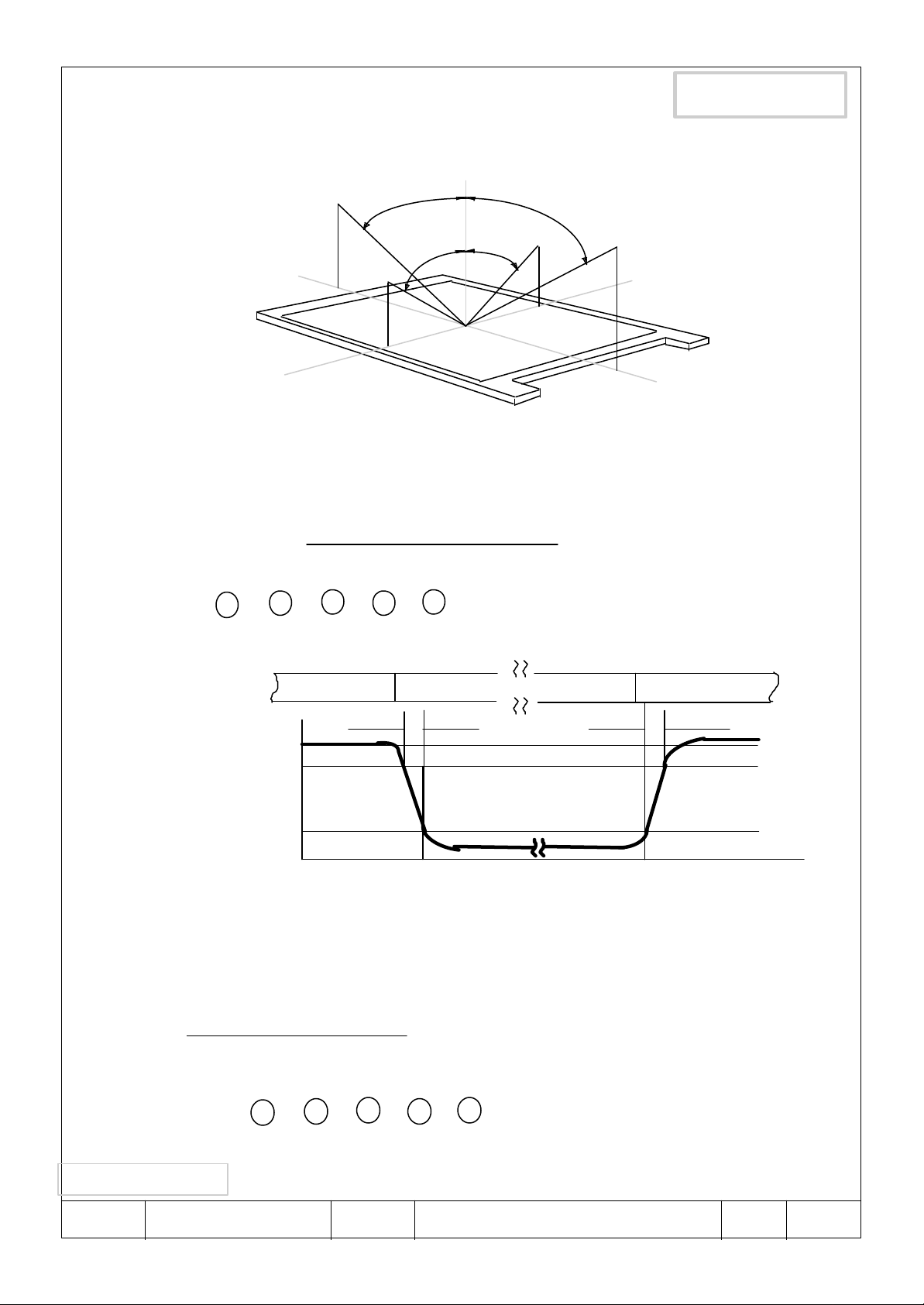
Note 1) Definition of Viewing Angle :
ΘL =90
o
x
ΘL
ΦL
Normal Line
o
Φ= 0
,
Θ= 0
ΦH
o
ΘR
Preliminary
12 O’clock
direction
y
ΦH= 90
o
6 O’clock
direction
ΦL= 90
o
Note 2) Definition of Contrast Ratio (CR) :
CR1 + CR2 + CR3 + CR4 + CR5
CR =
5
POINTS : , , , , at FIGURE OF NOTE 6)
4 5 9
7
10
Note 3) Definition of Response time :
Display data
White(TFT OFF)
Black(TFT ON)
TR
Optical
Response
100%
90%
10%
0%
x’y’
ΘR=90
White(TFT OFF)
TF
o
Note 4) Definition of Average Luminance of White : measure the luminance of white at 5 points.
Average Luminance of White ( Y L,AVE )
YL4 + YL5 + YL7 + YL9 + YL10
Y L,AVE =
5
POINTS : , 5 , , , at FIGURE OF NOTE 6)
4 5 9
7
10
Samsung Secret
Doc.No. Rev.No Page / 24LTN150PG-L03 804-000-G-040324
Time
Page 9

Preliminary
Note 5) After stabilizing and leaving the panel alone at a given temperature for 30 minutes, the measurement
should be executed. Measurement should be execut ed in a stable, windless,and dark room.
30 minutes after lighting the back-light. This should be measured in the center of screen.
Lamp current : 6.0 mA
Environment condition : Ta = 25 ± 2 ℃
Photo detector
( TOPCON BM-5A
PR-650)
Field = 2
TFT-LCD module
Optical characteristics measurement setup
Note 6) Definition of 13 points white variation (?W ), CR variation( CVER ) [ ~ ]
δL
Maximum luminance of 13 points
=
Minimum luminance of 13 points
45 979
13 12
256 512 768
o
Center of the screen
δC
50 cm
R
=
LCD panel
1 13
Maximum CR of 13 points
Minimum CR of 13 points
VIEW AREA
11
45
Samsung Secret
10
8
5
3
7
2
9
6
4
1
Doc.No. Rev.No Page / 24LTN150PG-L03 904-000-G-040324
192
384
576
723
(lines)
: test point
Page 10

3. ELECTRICAL CHARACTERISTICS
Preliminary
3.1 TFT LCD MODULE
ITEM SYMBOL MIN TYP MAX UNIT NOTE
Voltage of Power Supply VDD 3.0 3.3 3.6 V
Differential Input
Voltage for LVDS
Receiver Threshold
Vsync Frequency fv - 60 - Hz
Hsync Frequency fH - 63.98 - KHz
Main Frequency fDCLK 42.7 54 85 MHz
Rush Current IRUSH - - 1.5 A (4)
Current of
Power Supply
High
Low
White
Mosaic (2),(3)*b
Max
Pattern
VIH - - +100 mV
VIL -100 - - mV
- 430 - mA (2),(3)*a
IDD - 450 - mA
-
550 600
mA
Ta = 25 ± 2 ℃
VCM=+1.2V
(2),(3)*c
Note (1) Display data pins and timing signal pins should be connected.(GND=0V)
(2) fV=60Hz, fDCLK =54MHZ, Vdd = 3.3V , DC Current.
(3) Power dissipation pattern
*a) White Pattern *b) Mosaic Pattern
VIEW AREA
Display Brightest Gray Level
Display Darkest Gray Level
Samsung Secret
Doc.No. Rev.No Page / 24LTN150PG-L03 1004-000-G-040324
Page 11

*c) Maximum Power pattern : 1dot vertical stripe
4) Rush current measurement condition
Preliminary
R G B R G B R G B R G
G B R G B R G B R GR
G B R G B R G B R G
R
R G B R G B R G B R G
CONTROL SIGNAL
(HIGH to LOW)
3.3V
R1
47K
R2
1K
12V
C3
1uF
R3
47K
VDD rising time is 470us
0.1VDD
GND
M1
2SK1059
C2
10000pF
0.9VDD
M2
2SK1399
FUSE
470us
VDD ( LCD INPUT)
C1
1uF
3.3V
Samsung Secret
Doc.No. Rev.No Page / 24LTN150PG-L03 1104-000-G-040324
Page 12

3.2 BACK-LIGHT UNIT
The backlight system is an edge - lighting type with a single CCFT ( Cold Cathode Fluorescent Tube ).
The characteristics of a single lamp are shown in the following tables.
INVERTER : Ambit / Sumida
Preliminary
Ta = 25 ± 2 ℃
ITEM
Lamp Current IL 2.0 6.0 7.0 (1)
Lamp Voltage
Frequency
Operating Life Time Hr 10,000 Hour- - (4)
Startup Voltage
Note) The waveform of the inverter output voltage must be area symmetric and the design of the inverter
must have specifications for the modularized lamp.
The performance of the backlight, for example life time or brightness, is much influenced by the
characteristics of the DC -AC inverter for the lamp. So all the parameters of an inverter should be carefully
designed so as not to produce too much leakage current from high-voltage output of the inverter.
When you design or order the inverter, please make sure that a poor lighting caused by the mismatch of
the backlight and the inverter(miss lighting, flicker, etc.) never occur. When you confirm it, the module
should be operated in the same condition as it is installed in your instrument.
VL
fL
VS
VS - - sec
50 (2)
- WPower Consumption PL - (3)
-
60 65
3.93
-
1250
1450
1
mArms
Vrms
kHz
Vrms
Vrms
NOTEUNITMAXTYPMINSYMB
IL=6.0mA655
25?C
0 ?C
(5)Lamp Startup Time
Note (1) Lamp current is measured with a high frequency current meter as shown below.
HOT : BLUE
LCD
MODULE
(2) Lamp frequency may produce interference with horizontal synchronous frequency and this
may cause line flow on the display. Therefore lamp frequency should be detached from the
horizontal synchronous frequency and its harmonics as far as possible in order to avoid interference.
(3) refer to IL X VL to calculate.
(4) Life time (Hr) of a lamp can be defined as the time in which it continues to operate under the
condition Ta = 25 ± 2 ℃ and IL = 6.0 mArms until one of the following event occurs.
1. When the brightness becomes 50% or lower than the original.
(5) The voltage above this value should be applied to the lamp for more than 1 second to startup
Otherwise the lamp may not be turned on.
1
COLD : WHITE
2
No 2 Pin is VLOW.
A
INVERTER
Ambit / Sumida
Samsung Secret
Doc.No. Rev.No Page / 24LTN150PG-L03 1204-000-G-040324
Page 13

4. BLOCK DIAGRAM
4.1 TFT LCD Module
Preliminary
I2 C bus
Input-
Connector
FI-XB30S-HF10
or Compatible
LVDS
DC-DC
Converter
EDID
EEPROM
LVDS Input/RSDS Output
Timing Controller
Gamma
Generator
VCOM
Generator
SOURCE PCB
RSDS
Source
Driver
IC
15.0” SXGA+
TFT-LCD Panel
Gate Driver IC
Video Signal
Control Signal
VCOM
Gamma
DVDD
AVDD
Von/Voff
4.2 BACKLIGHT UNIT
Reflector
LAMP
Note) The output of the inverter may change according to the mat erial of the reflector.
1
HOT BLUE
COLD WHITE
2
Samsung Secret
Doc.No. Rev.No Page / 24LTN150PG-L03 1304-000-G-040324
Page 14

5. INPUT TERMINAL PIN ASSIGNMENT
5.1. Input Signal & Power LVDS, Connector : (JAE, FI-XB30SRL-HF11)
Preliminary
PIN NO SYMBOL POLARITY REMARK
1
2
3
4
5
6
7
8
9
10
11
12
13
14
Vss
VDD
VDD POWER SUPPLY +3.3V
VEEDID
BIST
CLKEDID N/A (DDC Clock)
DATAEDID N/A (DDC data)
O_RxIN0-
O_RxIN0+
Vss Ground
O_RxIN1-
O_RxIN1+
Vss Ground
O_RxIN2-
Ground
POWER SUPPLY +3.3V
N/A (DDC 3.3V Power)
Panel BIST control
LVDS Differential Data INPUT (Odd R0-R5,G0)
LVDS Differential Data INPUT (Odd R0-R5,G0)
LVDS Differential Data INPUT (Odd G1-G5,B0-B1)
LVDS Differential Data INPUT (Odd G1-G5,B0-B1)
LVDS Differential Data INPUT (Odd B1-B5,Sync,DE)
FUNCTION
Negative
Positive
Negative
Positive
Negative
15
16
17
18
19
20
21
22
23
24
25
26
27
28
29
O_RxIN2+
Vss Ground
O_RxCLK-
O_RxCLK+
Vss Ground
E_RxIN0-
E_RxIN0+
Vss
E_RxIN1-
E_RxIN1+
Vss Ground
E_RxIN2- LVDS Differential Data INPUT (Even B1-B5,Sync,DE)
E_RxIN2+
Vss Ground
E_RxCLK-
LVDS Differential Data INPUT (Odd B1-B5,Sync,DE)
LVDS Differential Data INPUT (Odd Clock)
LVDS Differential Data INPUT (Odd Clock)
LVDS Differential Data INPUT (Even R0 -R5,G0)
LVDS Differential Data INPUT (Even R0 -R5,G0)
Ground
LVDS Differential Data INPUT (Even G1-G5,B0-B1)
LVDS Differential Data INPUT (Even G1-G5,B0-B1)
LVDS Differential Data INPUT (Even B1-B5,Sync,DE)
LVDS Differential Data INPUT (Even Clock)
Positive
Negative
Positive
Negative
Positive
Negative
Positive
Negative
Positive
Negative
30
Samsung Secret
E_RxCLK+
LVDS Differential Data INPUT (Even Clock)
Doc.No. Rev.No Page / 24LTN150PG-L03 1404-000-G-040324
Positive
Page 15

Preliminary
5.2 LVDS Interface : Transmitter DS90CF363 or Compatible
LVDS for Odd pixel
Pin No. Name RGB Signal Pin No. Name RGB Signal
44 TxIN0 RO0 12 TxIN11 GO5
45 TxIN1 RO1 13 TxIN12 BO0
47 TxIN2 RO2 15 TxIN13 BO1
48 TxIN3 RO3 16 TxIN14 BO2
1 TxIN4 RO4 18 TxIN15 BO3
3 TxIN5 RO5 19 TxIN16 BO4
4 TxIN6 GO0 20 TxIN17 BO5
6 TxIN7 GO1 22 TxIN18 Hsync
7 TxIN8 GO2 23 TxIN19 Vsync
9 TxIN9 GO3 25 TxIN20 DE
10 TxIN10 GO4 26 TxCLK IN Clock
LVDS for Even pixel
Pin No. Name RGB Signal Pin No. Name RGB Signal
44 TxIN0 RE0 12 TxIN11 GE5
45 TxIN1 RE1 13 TxIN12 BE0
47 TxIN2 RE2 15 TxIN13 BE1
48 TxIN3 RE3 16 TxIN14 BE2
1 TxIN4 RE4 18 TxIN15 BE3
3 TxIN5 RE5 19 TxIN16 BE4
4 TxIN6 GE0 20 TxIN17 BE5
6 TxIN7 GE1 22 TxIN18 Hsync
7 TxIN8 GE2 23 TxIN19 Vsync
9 TxIN9 GE3 25 TxIN20 DE
10 TxIN10 GE4 26 TxCLK IN Clock
Samsung Secret
Doc.No. Rev.No Page / 24LTN150PG-L03 1504-000-G-040324
Page 16

Flat Link Interface
Preliminary
Graphics controller
36-bit
ODD RED0
ODD RED1
ODD RED2
ODD RED3
ODD RED4
ODD RED5
ODD GREEN0
ODD GREEN1
ODD GREEN2
ODD GREEN3
ODD GREEN4
ODD GREEN5
ODD BLUE0
ODD BLUE1
ODD BLUE2
ODD BLUE3
ODD BLUE4
ODD BLUE5
Hsync
Vsync
Enable
CLOCK
EVEN RED0
EVEN RED1
EVEN RED2
EVEN RED3
EVEN RED4
EVEN RED5
EVEN GREEN0
EVEN GREEN1
EVEN GREEN2
EVEN GREEN3
EVEN GREEN4
EVEN GREEN5
EVEN BLUE0
EVEN BLUE1
EVEN BLUE2
EVEN BLUE3
EVEN BLUE4
EVEN BLUE5
Hsync
Vsync
Enable
CLOCK
DS90CF363
or compatible
44
45
47
48
1
3
4
6
7
9
10
12
13
15
16
18
19
20
22
23
25
26
TxOUT0-
TxOUT0+
TxOUT1-
TxOUT1+
TxOUT2-
TxOUT2+
TxCLKOUT-
TxCLKOUT+
DS90CF363
or compatible
44
45
47
48
1
3
4
6
7
9
10
12
13
15
16
18
19
20
22
23
25
26
TxOUT0-
TxOUT0+
TxOUT1-
TxOUT1+
TxOUT2-
TxOUT2+
TxCLKOUT-
TxCLKOUT+
41
40
39
38
35
34
33
32
41
40
39
38
35
34
33
32
11
12
14
15
17
18
20
21
23
24
26
27
29
30
LVDS+I/F IC
8
100 Ω
9
100 Ω
100 Ω
100 Ω
100 Ω
100 Ω
100 Ω
100 Ω
O_RxIN0O_RxIN0+
O_RxIN1O_RxIN1+
RxIN2RxIN2+
RxCLKRxCLK+
E_RxIN0E_RxIN0+
E_RxIN1E_RxIN1+
E_RxIN2E_RxIN2+
E_RxCLKE_RxCLK+
Note : The LCD Module uses a 100ohm resistor between positive an d negative lines of each
receiver input.
Samsung Secret
Doc.No. Rev.No Page / 24LTN150PG-L03 1604-000-G-040324
Page 17

5.3 BACK LIGHT UNIT
Preliminary
Connector : JST BHSR - 02VS -1
Pin NO.
1
2
Symbol
HOT
COLD
Color
Blue
White
5.4 Timing Diagrams of LVDS For Transmission
TxCLKOUT
RxCLK IN
T/7
Function
High Voltage
Ground
T
Rx IN2
Rx IN1
RxOUT26 RxOUT25 RxOUT22RxOUT24 RxOUT21 RxOUT20 RxOUT19
DE
T/7
RxOUT18 RxOUT15 RxOUT13RxOUT14 RxOUT12 RxOUT9 RxOUT8
T/7
RxOUT7 RxOUT6 RxOUT3RxOUT4 RxOUT2 RxOUT1 RxOUT0
G0 R4R5 R2 R1 R0
Vsync B2Hsync B5 B3B4
G4B1 G5B0 G3 G2 G1
R3
Samsung Secret
Doc.No. Rev.No Page / 24LTN150PG-L03 1704-000-G-040324
Page 18

5.5 Input Signals, Basic Display Colors and Gray Scale of Each Color
Preliminary
COLOR
GRAY
SCALE
OF
RED
DATA SIGNAL
DISPLAYCOLOR
R0 G0 B0 B5G5R5R2 G2 B2 B4G4R4R1 G1 B1 B3G3R3
BLACK
BLUE
GREEN
MAGENTA 1 1 1 1 1 1 0 0 0 0 0 0 1 1 1 1 1 1 -
YELLOW 1 1 1 1 1 1 1 1 1 1 1 1 0 0 0 0 0 0 -
WHITE 1 1 1 1 1 1 1 1 1 1 1 1 1 1 1 1 1 1 -
BLACK 0 0 0 0 0 0 0 0 0 0 0 0 0 0 0 0 0 0 R0
DARK
LIGHT
0 0 0 0 0 0 0 0 0 0 0 0 0 0 0 0 0 0 0 0 0 0 0 0 0 0 0 0 0 0 1 1 1 1 1 1 -
0 0 0 0 0 0 1 1 1 1 1 1 0 0 0 0 0 0 0 0 0 0 0 0 1 1 1 1 1 1 1 1 1 1 1 1 -CYAN
1 1 1 1 1 1 0 0 0 0 0 0 0 0 0 0 0 0 -RED
1 0 0 0 0 0 0 0 0 0 0 0 0 0 0 0 0 0 R1
0 1 0 0 0 0 0 0 0 0 0 0 0 0 0 0 0 0 R2
: : : : : : : : : : : : : : : : : :
: : : : : : : : : : : : : : : : : :
1 0 1 1 1 1 0 0 0 0 0 0 0 0 0 0 0 0 R61
0 1 1 1 1 1 0 0 0 0 0 0 0 0 0 0 0 0 R62
RED GREEN BLUE
GRAY
SCALE
LEVEL
R3~R60
GRAY
SCALE
OF
GREEN
GRAY
SCALE
OF
BLUE
RED
BLACK 0 0 0 0 0 0 0 0 0 0 0 0 0 0 0 0 0 0 G0
DARK
LIGHT
GREEN
BLACK 0 0 0 0 0 0 0 0 0 0 0 0 0 0 0 0 0 0 B0
DARK
LIGHT
GREEN
1 1 1 1 1 1 0 0 0 0 0 0 0 0 0 0 0 0 R63
0 0 0 0 0 0 1 0 0 0 0 0 0 0 0 0 0 0 G1
0 0 0 0 0 0 0 1 0 0 0 0 0 0 0 0 0 0 G2
: : : : : : : : : : : : : : : : : :
: : : : : : : : : : : : : : : : : :
0 0 0 0 0 0 1 0 1 1 1 1 0 0 0 0 0 0 G61
0 0 0 0 0 0 0 1 1 1 1 1 0 0 0 0 0 0 G62
0 0 0 0 0 0 1 1 1 1 1 1 0 0 0 0 0 0 G63
0 0 0 0 0 0 0 0 0 0 0 0 1 0 0 0 0 0 B1
0 0 0 0 0 0 0 0 0 0 0 0 0 1 0 0 0 0 B2
: : : : : : : : : : : : : : : : : :
: : : : : : : : : : : : : : : : : :
0 0 0 0 0 0 0 0 0 0 0 0 1 0 1 1 1 1 B61
0 0 0 0 0 0 0 0 0 0 0 0 0 1 1 1 1 1 B62
0 0 0 0 0 0 0 0 0 0 0 0 1 1 1 1 1 1 B63
G3~G60
B3~B60
Note 1) Definition of gray :
Rn: Red gray, Gn: Green gray, Bn: Blue gray (n=gray level)
Note 2)Input signal: 0 =Low level voltage, 1=High level voltage
Samsung Secret
Doc.No. Rev.No Page / 24LTN150PG-L03 1804-000-G-040324
Page 19

5.6 Pixel Format in the display
Pixel 1 Pixel 1400
Preliminary
Line 1
Line 1050
R G B R G B
R G B R G B
LTN150PG-L03 Panel
R G B R G B R G B R G B
Samsung Secret
Doc.No. Rev.No Page / 24LTN150PG-L03 1904-000-G-040324
Page 20

6. INTERFACE TIMING
6.1 Timing Parameters
Preliminary
Signal Item Symbol MIN TYP MAX
Frame Frequency
Vertical Active
Display Term
One Line
Scanning Time
Horizontal Active
Display Term
Cycle
Display Period
Cycle
Display Period
6.2 Timing diagrams of interface signal
VD
T
Unit
TV
TVD
TH
THD
V
T
- 700 clocks
-- 1066 lines
-- 1050 lines
-- 844 clocks
-
Note
(1 )
DE
TH
DCLK
C
T
HD
T
DE
DATA
SIGNALS
Note : All input condition(level&timing) for SN75LVDS88 are the same with those of LPD11826 or compatible.
Samsung Secret
Valid display data ( 1024 pixel)
Doc.No. Rev.No Page / 24LTN150PG-L03 2004-000-G-040324
Page 21

6.3 Power ON/OFF Sequence
Preliminary
: To prevent a latch -up or DC operation of the LCD module, the power on/off sequence
shall be as shown below.
Power Supply
V DD
0V
0.5< T1 ≤10 msec
0 < T2 ≤50 msec
0 < T3 ≤50 msec
500msec ≤ T4
0 V
Back-light
200 msec≤T5
200 msec≤T6
0.1 VDD
Signals
0.9 VDD 0.9 VDD
0.1 VDD
T1
T3
T2
VALID
Power On
50% 50%
Power Off
T5 T6
Power ON/OFF Sequence
T4
T1 : Vdd rising time from 10% to 90%
T2 : The time from Vdd to valid data at power ON.
T3 : The time from valid data off to Vdd off at power Off.
T4 : Vdd off time for Windows restart
T5 : The time from valid data to B/L enable at power ON.
T6 : The time from valid data off to B/L disable at power Off.
NOTE.
(1) The supply voltage of the external system for the module input should be the same
as the definition of VDD.
(2) Apply the lamp voltage within the LCD operation range. W hen the backlight turns on
before the LCD operation or the LCD turns off before th e backlight turns off, the
display may momentarily become white.
(3) In case of VDD = off level, please keep the level of input signals on the low or keep
a high impedance.
(4) T4 should be measured after the module has been fully discharged between power
off and on period.
(5) Interface signal shall not be kept at high impedance when the power is on.
Samsung Secret
Doc.No. Rev.No Page / 24LTN150PG-L03 2104-000-G-040324
Page 22

7. Mechanical Outline Dimension
It will be attached with PDF file
Preliminary
Samsung Secret
Doc.No. Rev.No Page / 24LTN150PG-L03 2204-000-G-040324
Page 23

8. GENERAL PRECAUTIONS
1. Handling
(a) When the module is assembled, It should be attached to the system firmly
using every mounting holes. Be careful not to twist and bend the modules.
(b) Refrain from strong mechanical shock and / or any force to the module. In addition to
damage, this may cause improper operation or damage to the module and CCFT backlight.
(c) Note that polarizers are very fragile and could be easily damaged. Do not press or scratch
the surface harder than a HB pencil lead.
(d) Wipe off water droplets or oil immediately. If you leave the droplets for a long time,
Staining and discoloration may occur.
(e) If the surface of the polarizer is dirty, clean it using some absorbent cotton or soft cloth.
(f) The desirable cleaners are water, IPA(IsoprophylAlcohol) or Hexane.
Do not use Keptone type materials(ex. Acetone), Ethyl alcohol, Toluene, Ethyl acid or Methyl
chloride. It might permanent damage to the polarizer due to chemical reaction.
Preliminary
(g) If the liquid crystal material leaks from the panel, it should be kept away from the eyes or
mouth . In case of contact with hands, legs or clothes, it must be washed away thoroughly
with soap.
(h) Protect the module from static , it may cause damage to the C-MOS Gate Array IC.
(i) Use fingerstalls with soft gloves in order to keep displ ay clean during the incoming
inspection and assembly process.
(j) Do not disassemble the module.
(k) Do not pull or fold the lamp wire.
(l) Do not adjust the variable resistor which is located on the back side.
(m) Protection film for polarizer on the module shall be slowly peeled off just before use so
that the electrostatic charge can be minimized.
(n) Pins of I/F connector shall not be touched directly with bare hands.
Samsung Secret
Doc.No. Rev.No Page / 24LTN150PG-L03 2304-000-G-040324
Page 24

2. STORAGE
(a) Do not leave the module in high temperature, and high humidity for a long time.
It is highly recommended to store the module with temperature from 0 to 35?C and
relative humidity of less than 70%.
(b) Do not store the TFT-LCD module in direct sunlight.
(c) The module shall be stored in a dark place. It is prohibited to apply sunlight or fluorescent
light during the store.
3. OPERATION
(a) Do not connect,disconnect the module in the “Power On”condition.
(b) Power supply should always be turned on/off by follow ing item 6.3
“ Power on/off sequence “.
(c) Module has high frequency circuits. Sufficient suppression to the electromagnetic
interference shall be done by system manufacturers. Grounding and shielding methods
may be important to minimize the interference.
Preliminary
(d) The cable between the backlight connector and its inv erter power supply shall be a
minimized length and be connected directly . The lon ger cable between the backlight
and the inverter may cause lower luminance of lamp(CCFT) and may require higher
startup voltage (Vs).
(e) The standard limited warranty is only applicable when the module is used for general
notebook applications. If used for purposes other than as specified, SEC is not to be
held reliable for the defective operations. It is strongly recommended to contact SEC
to find out fitness for a particular purpose.
4. OTHERS
(a) Ultra-violet ray filter is necessary for outdoor operation.
(b) Avoid condensation of water. It may result in improper operation or disconnection
of electrode.
(c) Do not exceed the absolute maximum rating value. ( the supply voltage variation, input
voltage variation, variation in part contents and environmental temperature, so on)
Otherwise the module may be damaged.
(d) If the module displays the same pattern continuously for a long period of time,it can be
the situation when the image “sticks”to the screen.
(e) This module has its circuitry PCB’s on the rear side and should be handled carefully in
order not to be stressed.
Samsung Secret
Doc.No. Rev.No Page / 24LTN150PG-L03 2404-000-G-040324
Page 25

 Loading...