

Page 1
Global LCD Panel Exchange Center
www.panelook.com
Approval
T O
DATE
SAMSUNG TFT-LCD
SAMSUNG TFT-LCD
MODEL NO.:LTN150PG-L02
MODEL NO.:LTN150PG-L02
: Dell /Compal
: Set. 19. 2003
Any Modification of Spec is not allowed without SEC’ permission
APPROVED BY :
PREPARED BY : Technical Customer Service Team
SAMSUNG ELECTRONICS CO., LTD.SAMSUNG ELECTRONICS CO., LTD.
Doc.No. Rev.No Page / 32LTN150PG-L02 104-A00-S-030919
One step solution for LCD / PDP / OLED panel application: Datasheet, inventory and accessory!
www.panelook.com
Page 2
Global LCD Panel Exchange Center
CONTENTS
www.panelook.com
Approval
Revision History
General Description
1. Absolute Maximum Ratings
1.1 Absolute Ratings of environment
1.2 Electrical Absolute Ratings
2. Optical Characteristics
3. Electrical Characteristics
3.1 TFT LCD Module
3.2 Backlight Unit
4. Block Diagram
4.1 TFT LCD Module
4.2 Backlight Unit
5. Input Terminal Pin Assignment
5.1 Input Signal & Power
5.2 LVDS Interface
5.3 Backlight Unit
5.4 Timing Diagrams of LVDS For Transmitting
5.5 Input Signals, Basic Display Colors and Gray Scale of Each Color.
5.6 Pixel format
-------------------( 3 )
-------------------( 4 )
-------------------( 5 )
-------------------( 7 )
-------------------( 10 )
-------------------( 14 )
-------------------( 16 )
6. Interface Timing
6.1 Timing Parameters(DE Mode)
6.2 Timing Diagrams of interface Signal (DE Mode)
6.3 Power ON/OFF Sequence
7. Outline Dimension
8. Packing
9.Markings and Others
10. GENERAL PRECAUTIONS
Appendix 1.EDID
Appendix 2.Inverter spec.
Doc.No. Rev.No Page / 32LTN150PG-L02 204-A00-S-030919
-------------------( 22 )
-------------------( 24 )
-------------------( 25 )
-------------------( 26 )
-------------------( 28 )
One step solution for LCD / PDP / OLED panel application: Datasheet, inventory and accessory!
www.panelook.com
Page 3
Global LCD Panel Exchange Center
www.panelook.com
Date
Apr. 16, 2003 P00 All
Set. 01, 2003 A00 All
Rev.No. Summary
Page
16
24
Appendix To update EDID
REVISION HISTORY
REVISION HISTORY
LTN150PG-L02 model rev.P00 specification was First issued.
To correct typos
To correct the input connector (JAE, FI-XB30SRL-HF11)
To change the length of lamp wire tape (52mm60mm)
Approval
Doc.No. Rev.No Page / 32LTN150PG-L02 304-A00-S-030919
One step solution for LCD / PDP / OLED panel application: Datasheet, inventory and accessory!
www.panelook.com
Page 4
Global LCD Panel Exchange Center
GENERAL DESCRIPTION
DESCRIPTION
LTN150PG-L01 is a color active matrix TFT (Thin Film Transistor) liquid crystal display
(LCD) that uses amorphous silicon TFT as a switching devices. This model is composed of
a TFT LCD panel, a driver circuit and a backlight system. The resolution of a 15.0" contains
1400 x 1050 pixels and can display up to 262,144 colors. 6 O'clock direction is the Optimum
viewing angle.
FEATURES
• Thin and light weight
• High contrast ratio
• SXGA-Plus (1400x1050 pixels) resolution
• Low power consumption
• DE (Data enable) only mode.
• LVDS Interface with 2 pixel / clock (2 channel)
www.panelook.com
Approval
APPLICATIONS
• Notebook PC and desktop monitors
• Display terminals for AV application products
• Monitors for Industrial machine
• If the usage of this product is not for PC application, but for others, please contact SEC
GENERAL INFORMATION
ITEM SPECIFICATION
Display area 304.1(H)X228.1(V) (15.0” diagonal)
Driver element a-si TFT active matrix
Display colors 262,144
Number of pixel 1400 x 1050 (SXGA-Plus)
Pixel arrangement RGB vertical stripe
UNIT
mm
pixel
NOTE
Pixel pitch 0.2175(H) x 0.2175(V)
Normally whiteDisplay Mode
Surface treatment
Doc.No. Rev.No Page / 32LTN150PG-L02 404-A00-S-030919
One step solution for LCD / PDP / OLED panel application: Datasheet, inventory and accessory!
HAZE 25, HARD-COATING 3H
mm
www.panelook.com
Page 5
Global LCD Panel Exchange Center
www.panelook.com
Mechanical Information
ITEM TYP. MAX. NOTE
Horizontal (H)
Module
Size
Note (1) Depth of signal interface connector part.
Vertical (V)
Depth (D) -
Weight
MIN.
316.8
241.6
1. ABSOLUTE MAXIMUM RATINGS
1.1 ENVIRONMENTAL ABSOLUTE RATINGS
ITEM UNIT
Storage temperate
SYMBOL MIN. MAX.
T
STG
317.3
242.1 242.6
- 6.0
550g
-25 60
317.8
565g
O
Approval
Without Inverter
NOTE
C
(1)
Operating temperate
(Temperature of glass surface)
Shock ( non-operating )
Vibration (non-operating)
Note (1) Temperature and relative humidity range are shown in the figure below.
95 % RH Max. ( 40
Maximum wet - bulb temperature at 39
(2) 2ms, half sine wave, one time for ᇹX,ᇹY,ᇹZ.
(3) 10 300 10 Hz, Sweep rate 10 min, 30 min for X,Y,Z.
(4) At testing Vibration and Shock, the fixture in holding the Module to be tested have to be
hard and rigid enough so that the Module would not be twisted or bent by the fixture.
O
C ᆚTa)
100
95
80
60
40
T
OPR
Snop
Vnop
0
-
-
O
C or less. (Ta > 40 OC) No condensation.
Relative Humidity ( %RH)
Operating Range
50
220 G
1. 5
O
C
G
(1)
(2), (4)
(3), (4)
20
Storage Range
5
0
-40-20 0 2040 6080
Temperature (
O
C)
Doc.No. Rev.No Page / 32LTN150PG-L02 504-A00-S-030919
One step solution for LCD / PDP / OLED panel application: Datasheet, inventory and accessory!
www.panelook.com
Page 6
Global LCD Panel Exchange Center
www.panelook.com
1.2 ELECTRICAL ABSOLUTE RATINGS
(1) TFT LCD MODULE
ITEM SYMBOL MIN. MAX. UNIT NOTE
Power Supply Voltage
Logic Input Voltage V
NOTE (1) Within Ta ( 25 ᇹ2
Vcc
O
C )
Vss-0.3 4.0
IN
Vss-0.3
(2) BACK-LIGHT UNIT
ITEM SYMBOL
Lamp current I
Lamp frequency
L
L
F
MIN. UNIT. NOTE
3.0
50
MAX.
7.0
80 KHz
mA
Approval
( Vss = GND = 0 V)
V
VVcc + 0.3
rms
( 1 )
( 1 )
Ta = 25 ᇹ2 OC
(1)
(1)
NOTE (1) Permanent damage to the device may occur if maximum values are exceeded.
Functional operation should be restricted to the conditions described under Normal Operating
Conditions.
Doc.No. Rev.No Page / 32LTN150PG-L02 604-A00-S-030919
One step solution for LCD / PDP / OLED panel application: Datasheet, inventory and accessory!
www.panelook.com
Page 7
Global LCD Panel Exchange Center
2. OPTICAL CHARACTERISTICS
The following items are measured under stable conditions. The optical characteristics
should be measured in a dark room or equivalent state with the methods shown in Note
(5).
Measuring equipment : TOPCON BM-5A
www.panelook.com
Approval
ITEM SYMBOL CONDITION MIN. TYP. MAX. UNIT
Contrast Ratio
(5 Points)
Response
Time at 25
ఁ
Luminance
of White
Color
Chromaticity
( CIE )
Rising T
Falling
Red
Green
Blue
CR
T
YL
R
R
GX
GY
BX
BY
* Ta = 25 ± 2°C, V
DD=3.3V, fv= 60Hz, fDCLK=54MHz, IL = 6.3 mA
NOTE
300
R
F
-
-
-
10
15 20
200180
φ = 0,
X
Y
θ = 0
Normal
0.560
0.320
0.580
0.340
-
15
-
0.600
0.360
msec
cd/m
2
(1), (3)
(1), (4)
@6.3mm
Viewing
Angle
0.290
0.530
0.135
0.135
0.310
0.550
0.155
0.155
0.330
0. 570
0.175
0.175
(1), (5)
PR650
Viewing
Angle
13 Points
White Variation
White
Hor.
Ver.
WX
WY
θ
θ R
φ H
φ L
L
(at center point)
CR ᆚ10
0.293
0.309
60
60
45
45
0.313
0.333
0.329 0.349
-
-
-
-
-
-
-
-
2.0-
Degrees
(6)
Doc.No. Rev.No Page / 32LTN150PG-L02 704-A00-S-030919
One step solution for LCD / PDP / OLED panel application: Datasheet, inventory and accessory!
www.panelook.com
Page 8
Global LCD Panel Exchange Center
www.panelook.com
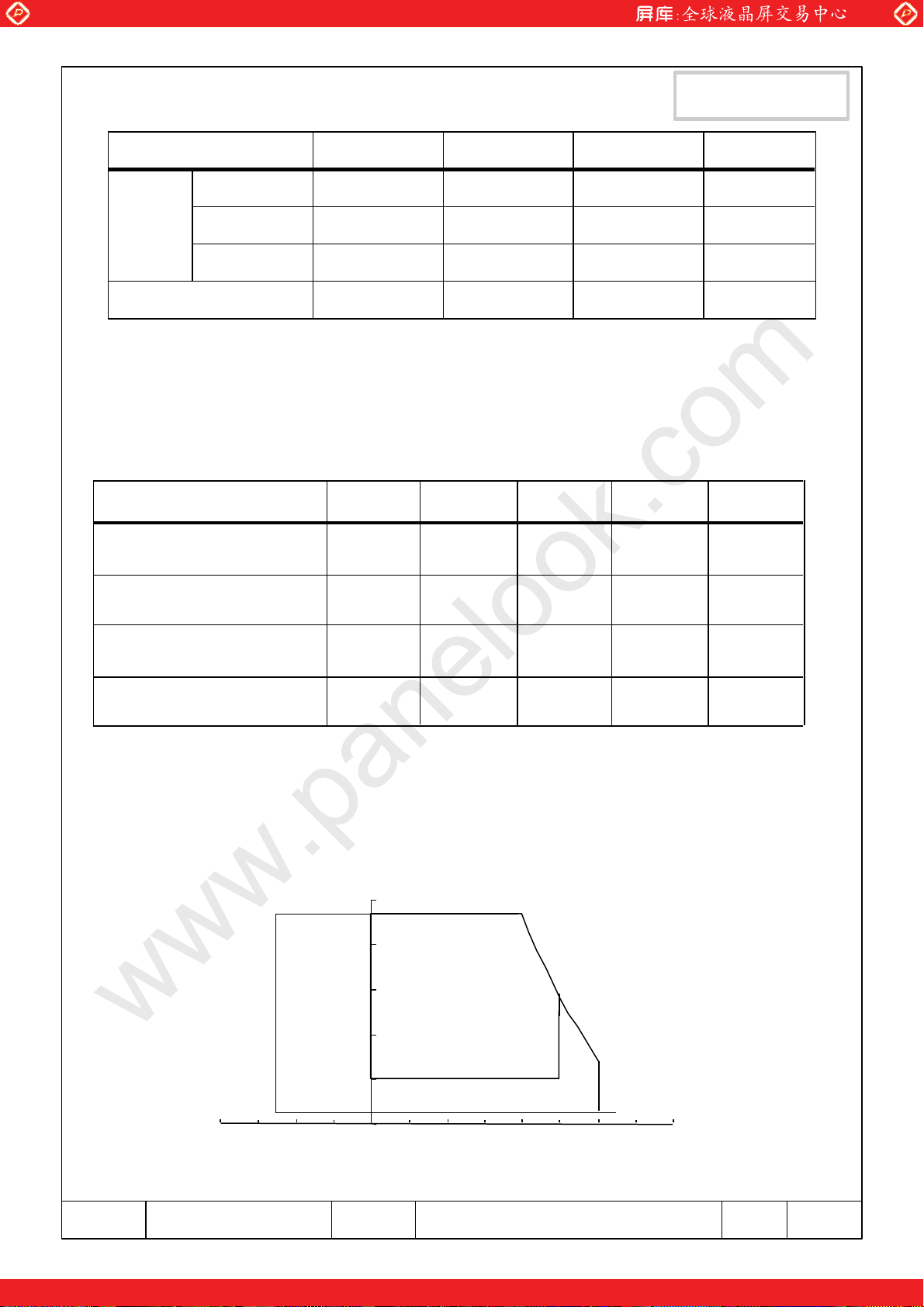
Note 1) Definition of Viewing Angle :
θ L
θL =90
o
x
6 O’ clock
direction
φL= 90
o
Note 2) Definition of Contrast Ratio (CR) :
CR1 + CR2 + CR3 + CR4 + CR5
CR =
φ L
5
Normal Line
o
θ = 0
φ = 0
,
φ H
Approval
o
θ R
12 O’ clock
y
direction
φH= 90
o
x’y’
o
=90
θ
R
POINTS : , , , , at FIGURE OF NOTE 6)
45 9
7
10
Note 3) Definition of Response time :
Display data
Optical
Response
White(TFT OFF)
100%
90%
Black(TFT ON)
TR
White(TFT OFF)
TF
10%
0%
Note 4) Definition of Average Luminance of White : measure the luminance of white at 5 points.
Average Luminance of White ( Y L,AVE )
Y
L4 + YL5 + YL7 + YL9 + YL10
Y L,AVE =
Time
5
POINTS : , 5 , , , at FIGURE OF NOTE 6)
45 9
7
10
Doc.No. Rev.No Page / 32LTN150PG-L02 804-A00-S-030919
One step solution for LCD / PDP / OLED panel application: Datasheet, inventory and accessory!
www.panelook.com
Page 9
Global LCD Panel Exchange Center
Note 5) After stabilizing and leaving the panel alone at a given temperature for 30 minutes, the measurement
should be executed. Measurement should be executed in a stable, windless,and dark room.
30 minutes after lighting the back-light. This should be measured in the center of screen.
Lamp current : 6.0 mA
Environment condition : Ta = 25 ± 2 °C
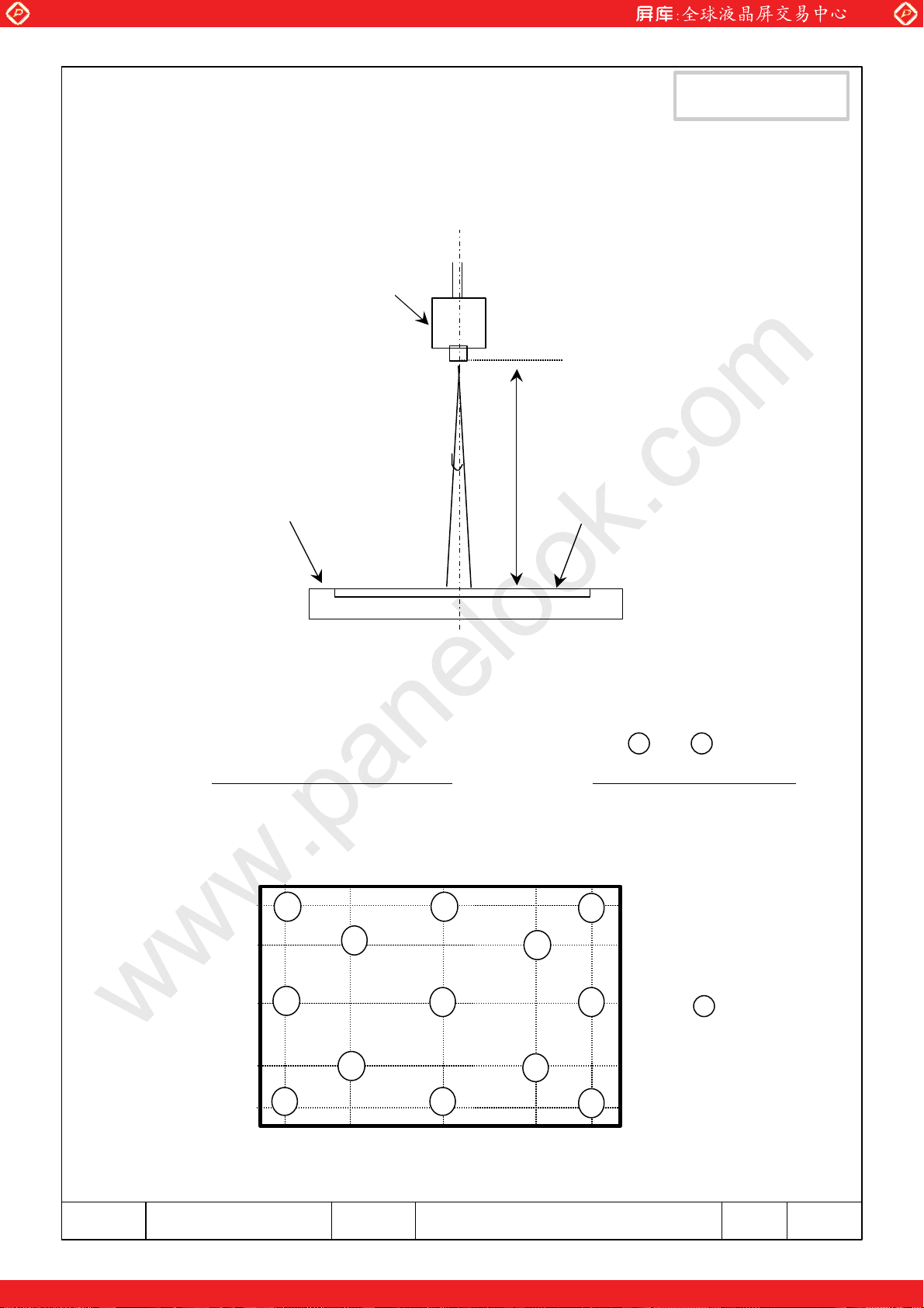
Photo detector
( TOPCON BM-5A)
www.panelook.com
Approval
Field = 2
TFT-LCD module
Optical characteristics measurement setup
Note 6) Definition of 13 points white variation (
δ L
Maximum luminance of 13 points
=
Minimum luminance of 13 points
45 979
13 12
256 512 768
o
Center of the screen
50 cm
LCD panel
δ
W ), CR variation( CVER ) [ ~ ]
δ C
R
=
11
113
Maximum CR of 13 points
Minimum C
45
R of 13 points
VIEW AREA
10
8
5
3
7
2
9
4
192
384
6
576
1
723
(lines)
: test point
Doc.No. Rev.No Page / 32LTN150PG-L02 904-A00-S-030919
One step solution for LCD / PDP / OLED panel application: Datasheet, inventory and accessory!
www.panelook.com
Page 10
Global LCD Panel Exchange Center
www.panelook.com
3. ELECTRICAL CHARACTERISTICS
3.1 TFT LCD MODULE
ITEM SYMBOL MIN TYP MAX UNIT NOTE
Voltage of Power Supply VDD 3.0 3.3 3.6 V
Differential Input
High
Voltage for LVDS
Receiver Threshold
Low
Vsync Frequency fv - 60 - Hz
Hsync Frequency f
Main Frequency f
Rush Current I
White
Current of
Power Supply
Mosaic (2),(3)*b
Max
Pattern
IH - - +100 mV
V
IL -100 - - mV
V
H - 63.98 - KHz
DCLK 42.7 54 85 MHz
RUSH - - 1.5 A (4)
- 430 - mA (2),(3)*a
DD - 450 - mA
I
-
550 600
mA
Approval
Ta=25 ± 2 º C
V
CM=+1.2V
(2),(3)*c
Note (1) Display data pins and timing signal pins should be connected.(GND=0V)
(2) f
V=60Hz, fDCLK =54MHZ, Vdd = 3.3V , DC Current.
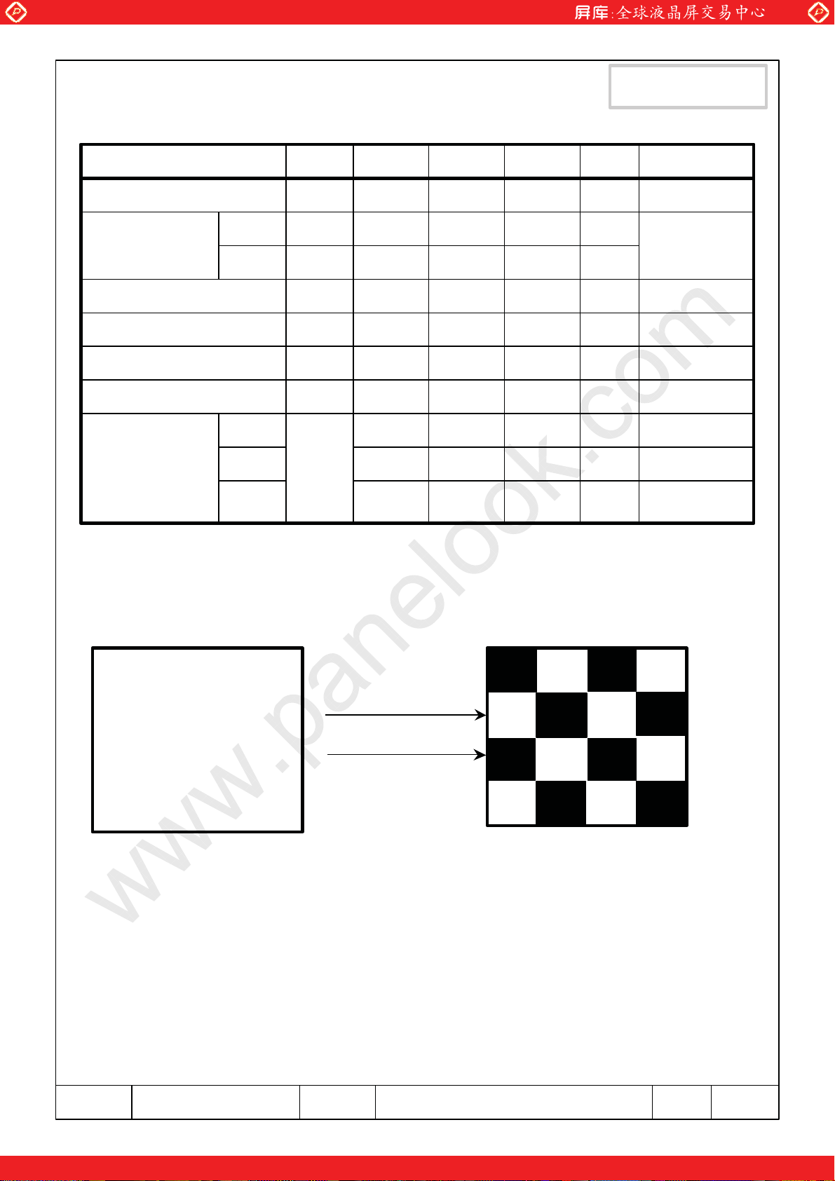
(3) Power dissipation pattern
*a) White Pattern *b) Mosaic Pattern
VIEW AREA
Display Brightest Gray Level
Display Darkest Gray Level
Doc.No. Rev.No Page / 32LTN150PG-L02 1004-A00-S-030919
One step solution for LCD / PDP / OLED panel application: Datasheet, inventory and accessory!
www.panelook.com
Page 11
Global LCD Panel Exchange Center
*c) Maximum Power pattern : 1dot vertical stripe
4) Rush current measurement condition
www.panelook.com
Approval
RGBRGBRGBRG
GBRGB RGB RG
R
R
GBRGB RGB RG
RGBRGBRGBRG
CONTROL SIGNAL
(HIGH to LOW)
3.3V
R1
47K
R2
1K
12V
V
R3
C3
1uF
DD rising time is 470us
47K
GND
C2
10000pF
0.1VDD
M1
2SK1059
M2
2SK1399
0.9VDD
FUSE
470us
VDD ( LCD INPUT)
C1
1uF
3.3V
Doc.No. Rev.No Page / 32LTN150PG-L02 1104-A00-S-030919
One step solution for LCD / PDP / OLED panel application: Datasheet, inventory and accessory!
www.panelook.com
Page 12
Global LCD Panel Exchange Center
www.panelook.com
mArms
rms
V
kHz
V
rms
V
rms
Approval
Ta=25 ± 2
NOTEUNITMAXTYPMINSYMB
IL=6.0mA655
25°C
0 °C
(5)
3.2 BACK-LIGHT UNIT
The backlight system is an edge - lighting type with a single CCFT ( Cold Cathode Fluorescent Tube ).
The characteristics of a single lamp are shown in the following tables.
INVERTER : Ambit / Sumida
ITEM
Lamp Current I
Lamp Voltage
Frequency
Power Consumption PL - (3)
Operating Life Time Hr 15,000 Hour- - (4)
Startup Voltage
Lamp Startup Time
Note) The waveform of the inverter output voltage must be area symmetric and the design of the inverter
must have specifications for the modularized lamp.
The performance of the backlight, for example life time or brightness, is much influenced by the
characteristics of the DC-AC inverter for the lamp. So all the parameters of an inverter should be carefully
designed so as not to produce too much leakage current from high-voltage output of the inverter.
When you design or order the inverter, please make sure that a poor lighting caused by the mismatch of
the backlight and the inverter(miss lighting, flicker, etc.) never occur. When you confirm it, the module
should be operated in the same condition as it is installed in your instrument.
L 2.0 6.0 7.0 (1)
VL
fL
VS
VS - - sec1
45 (2)
-W
-
60 80
4.0
1150
1380
o
C
Note (1) Lamp current is measured with a high frequency current meter as shown below.
HOT : BLUE
LCD
MODULE
(2) Lamp frequency may produce interference with horizontal synchronous frequency and this
may cause line flow on the display. Therefore lamp frequency should be detached from the
horizontal synchronous frequency and its harmonics as far as possible in order to avoid interference.
(3) refer to I
(4) Life time (Hr) of a lamp can be defined as the time in which it continues to operate under the
condition Ta = 25 ±2
1. When the brightness becomes 50% or lower than the original.
(5) The voltage above this value should be applied to the lamp for more than 1 second to startup
Otherwise the lamp may not be turned on.
L X VL to calculate.
o
C and IL = 6.0 mArms until one of the following event occurs.
1
2
No 2 Pin is V
COLD : WHITE
A
LOW.
INVERTER
Ambit / Sumida
Doc.No. Rev.No Page / 32LTN150PG-L02 1204-A00-S-030919
One step solution for LCD / PDP / OLED panel application: Datasheet, inventory and accessory!
www.panelook.com
Page 13
Global LCD Panel Exchange Center
3.3 INVERTER
Inverter : AMBIT/SUMIDA Ta = 25 ± 2°CTa = 25 ± 2°C
www.panelook.com
Approval
ITEM MIN
Input Voltage(Vin)
Open Circuit Voltage
PWM duty cycle
Optical
Efficiency
Electrical
Operating Frequency
PWM Frequency
Input Voltage Ripple - Vpp
Input Power Consumption
In-rush current
7.5 14.4
10 ±2
@SMB_DAT
FFH
20
-
-
-
TYP MAX
21.0
18001400
-
80
5545
210 Hz220200 Vin=14.4V
5.0
--
100
@SMB_DAT
00H
-
65
0.5
5.7
1.5
UNIT
mArms
Vrms
%
Nit/W--
%
kHz SMB_DAT=00H
W
A
After 30min turn on
at the center of LCD
Vin=14.4V @6.0mA(3)
Peak to peak value
NOTE
IL =6.0 mArms
Vin=14.4V
(1)
Iout=6.0mArms
Shutdown time
Start-up time
1.0-
--
1.4
0.1 (2)
Note
(1) Vin=14.4V, IL=6.0mA
(2) Inverter start-up time
(3) Efficiency should be calculated as below formulation.
Optical efficiency = output Brightness(nits) / Input power(watt)
Electrical efficiency = output power / input power
sec
sec
Doc.No. Rev.No Page / 32LTN150PG-L02 1304-A00-S-030919
One step solution for LCD / PDP / OLED panel application: Datasheet, inventory and accessory!
www.panelook.com
Page 14
Global LCD Panel Exchange Center
4. BLOCK DIAGRAM
4.1 TFT LCD Module
www.panelook.com
Approval
I2 C bus
Input-
Connector
FI-XB30S-HF10
or Compatible
LVDS
DC-DC
Converter
EDID
EEPROM
LVDS Input/RSDS Output
Timing Controller
Gamma
Generator
VCOM
Generator
SOURCE PCB
RSDS
Source
Driver
IC
15.0” SXGA+
TFT-LCD Panel
Gate Driver IC
Video Signal
Control Signal
VCOM
Gamma
DVDD
AVDD
Von/Voff
Doc.No. Rev.No Page / 32LTN150PG-L02 1404-A00-S-030919
One step solution for LCD / PDP / OLED panel application: Datasheet, inventory and accessory!
www.panelook.com
Page 15

Global LCD Panel Exchange Center
4.2 BACKLIGHT UNIT
Reflector
Note) The output of the inverter may change according to the material of the reflector.
www.panelook.com
LAMP
Approval
1
HOT BLUE
2
COLD WHITE
4.3 Inverter UNIT
- Input Connector : HONDA, LVC-D20SFYG
Data & CLK
DVdd
Input
Connector
AVdd
SMBUS
Controller
Driving
Controller
OVL & OCL
Detection
Transformer
Open lamp
Detection
Lamp
Connector
Doc.No. Rev.No Page / 32LTN150PG-L02 1504-A00-S-030919
One step solution for LCD / PDP / OLED panel application: Datasheet, inventory and accessory!
www.panelook.com
Page 16

Global LCD Panel Exchange Center
www.panelook.com
5. INPUT TERMINAL PIN ASSIGNMENT
5.1. Input Signal & Power LVDS, Connector : (JAE, FI-XB30SRL-HF11)
Approval
PIN NO SYMBOL POLARITY REMARK
1
2
3
4
5
6
7
8
9
10
11
12
13
14
Vss
VDD
VDD POWER SUPPLY +3.3V
VEEDID
BIST
CLKEDID N/A (DDC Clock)
DATAEDID N/A (DDC data)
O_RxIN0-
O_RxIN0+
Vss Ground
O_RxIN1-
O_RxIN1+
Vss Ground
O_RxIN2-
Ground
POWER SUPPLY +3.3V
N/A (DDC 3.3V Power)
Panel BIST control
LVDS Differential Data INPUT (Odd R0-R5,G0)
LVDS Differential Data INPUT (Odd R0-R5,G0)
LVDS Differential Data INPUT (Odd G1-G5,B0-B1)
LVDS Differential Data INPUT (Odd G1-G5,B0-B1)
LVDS Differential Data INPUT (Odd B1-B5,Sync,DE)
FUNCTION
Negative
Positive
Negative
Positive
Negative
15
16
17
18
19
20
21
22
23
24
25
26
27
28
29
O_RxIN2+
Vss Ground
O_RxCLK-
O_RxCLK+
Vss Ground
E_RxIN0-
E_RxIN0+
Vss
E_RxIN1-
E_RxIN1+
Vss Ground
E_RxIN2- LVDS Differential Data INPUT (Even B1-B5,Sync,DE)
E_RxIN2+
Vss Ground
E_RxCLK -
LVDS Differential Data INPUT (Odd B1-B5,Sync,DE)
LVDS Differential Data INPUT (Odd Clock)
LVDS Differential Data INPUT (Odd Clock)
LVDS Differential Data INPUT (Even R0-R5,G0)
LVDS Differential Data INPUT (Even R0-R5,G0)
Ground
LVDS Differential Data INPUT (Even G1-G5,B0-B1)
LVDS Differential Data INPUT (Even G1-G5,B0-B1)
LVDS Differential Data INPUT (Even B1-B5,Sync,DE)
LVDS Differential Data INPUT (Even Clock)
Positive
Negative
Positive
Negative
Positive
Negative
Positive
Negative
Positive
Negative
30
E_RxCLK +
LVDS Differential Data INPUT (Even Clock)
Positive
Doc.No. Rev.No Page / 32LTN150PG-L02 1604-A00-S-030919
One step solution for LCD / PDP / OLED panel application: Datasheet, inventory and accessory!
www.panelook.com
Page 17

Global LCD Panel Exchange Center
5.2 LVDS Interface : Transmitter DS90CF363 or Compatible
LVDS for Odd pixel
Pin No. Name RGB Signal Pin No. Name RGB Signal
44 TxIN0 RO0 12 TxIN11 GO5
45 TxIN1 RO1 13 TxIN12 BO0
47 TxIN2 RO2 15 TxIN13 BO1
48 TxIN3 RO3 16 TxIN14 BO2
1 TxIN4 RO4 18 TxIN15 BO3
3 TxIN5 RO5 19 TxIN16 BO4
www.panelook.com
Approval
4 TxIN6 GO0 20 TxIN17 BO5
6 TxIN7 GO1 22 TxIN18 Hsync
7 TxIN8 GO2 23 TxIN19 Vsync
9 TxIN9 GO3 25 TxIN20 DE
10 TxIN10 GO4 26 TxCLK IN Clock
LVDS for Even pixel
Pin No. Name RGB Signal Pin No. Name RGB Signal
44 TxIN0 RE0 12 TxIN11 GE5
45 TxIN1 RE1 13 TxIN12 BE0
47 TxIN2 RE2 15 TxIN13 BE1
48 TxIN3 RE3 16 TxIN14 BE2
1 TxIN4 RE4 18 TxIN15 BE3
3 TxIN5 RE5 19 TxIN16 BE4
4 TxIN6 GE0 20 TxIN17 BE5
6 TxIN7 GE1 22 TxIN18 Hsync
7 TxIN8 GE2 23 TxIN19 Vsync
9 TxIN9 GE3 25 TxIN20 DE
10 TxIN10 GE4 26 TxCLK IN Clock
Doc.No. Rev.No Page / 32LTN150PG-L02 1704-A00-S-030919
One step solution for LCD / PDP / OLED panel application: Datasheet, inventory and accessory!
www.panelook.com
Page 18

Global LCD Panel Exchange Center
Flat Link Interface
www.panelook.com
Approval
Graphics controller
36-bit
ODD RED0
ODD RED1
ODD RED2
ODD RED3
ODD RED4
ODD RED5
ODD GREEN0
ODD GREEN1
ODD GREEN2
ODD GREEN3
ODD GREEN4
ODD GREEN5
ODD BLUE0
ODD BLUE1
ODD BLUE2
ODD BLUE3
ODD BLUE4
ODD BLUE5
Hsync
Vsync
Enable
CLOCK
EVEN RED0
EVEN RED1
EVEN RED2
EVEN RED3
EVEN RED4
EVEN RED5
EVEN GREEN0
EVEN GREEN1
EVEN GREEN2
EVEN GREEN3
EVEN GREEN4
EVEN GREEN5
EVEN BLUE0
EVEN BLUE1
EVEN BLUE2
EVEN BLUE3
EVEN BLUE4
EVEN BLUE5
Hsync
Vsync
Enable
CLOCK
DS90CF363
or compatible
44
45
47
48
1
3
4
6
7
9
10
12
13
15
16
18
19
20
22
23
25
26
TxOUT0-
TxOUT0+
TxOUT1-
TxOUT1+
TxOUT2-
TxOUT2+
TxCLKOUT-
TxCLKOUT+
DS90CF363
or compatible
44
45
47
48
1
3
4
6
7
9
10
12
13
15
16
18
19
20
22
23
25
26
TxOUT0-
TxOUT0+
TxOUT1-
TxOUT1+
TxOUT2-
TxOUT2+
TxCLKOUT-
TxCLKOUT+
41
40
39
38
35
34
33
32
41
40
39
38
35
34
33
32
11
12
14
15
17
18
20
21
23
24
26
27
29
30
LVDS+I/F IC
8
100 Ω
9
100 Ω
100 Ω
100 Ω
100 Ω
100 Ω
100 Ω
100 Ω
O_RxIN0-
O_RxIN0+
O_RxIN1-
O_RxIN1+
RxIN2-
RxIN2+
RxCLK -
RxCLK+
E_RxIN0-
E_RxIN0+
E_RxIN1-
E_RxIN1+
E_RxIN2-
E_RxIN2+
E_RxCLK -
E_RxCLK +
Note : The LCD Module uses a 100ohm resistor between positive and negative lines of each
receiver input.
Doc.No. Rev.No Page / 32LTN150PG-L02 1804-A00-S-030919
One step solution for LCD / PDP / OLED panel application: Datasheet, inventory and accessory!
www.panelook.com
Page 19

Global LCD Panel Exchange Center
5.3 BACK LIGHT UNIT
www.panelook.com
Approval
Connector : JST BHSR - 02VS -1
Pin NO.
1
2
Symbol
HOT
COLD
Color
Blue
White
5.4 Timing Diagrams of LVDS For Transmission
TxCLK OUT
RxCLK IN
T/7
Function
High Voltage
Ground
T
Rx IN2
Rx IN1
RxOUT26 RxOUT25 RxOUT22RxOUT24 RxOUT21 RxOUT20 RxOUT19
DE
T/7
RxOUT18 RxOUT15 RxOUT13RxOUT14 RxOUT12 RxOUT9 RxOUT8
T/7
RxOUT7 RxOUT6 RxOUT3RxOUT4 RxOUT2 RxOUT1 RxOUT0
G0 R4R5 R2 R1 R0
Vsync B2Hsync B5 B3B4
G4B1 G 5B0 G3 G2 G1
R3
Doc.No. Rev.No Page / 32LTN150PG-L02 1904-A00-S-030919
One step solution for LCD / PDP / OLED panel application: Datasheet, inventory and accessory!
www.panelook.com
Page 20

Global LCD Panel Exchange Center
www.panelook.com
5.5 Input Signals, Basic Display Colors and Gray Scale of Each Color
DATA SIGNAL
RED GREEN BLUE
COLOR
GRAY
SCALE
OF
RED
DISPLAYCOLOR
R0 G0 B0 B5G5R5R2 G2 B2 B4G4R4R1 G1 B1 B3G3R3
BLACK
BLUE
GREEN
MAGENTA 1 1 1 1 1 1 0 0 0 0 0 0 1 1 1 1 1 1 -
YELLOW 1 1 1 1 1 1 1 1 1 1 1 1 0 0 0 0 0 0 -
WHITE 1 1 1 1 1 1 1 1 1 1 1 1 1 1 1 1 1 1 -
BLACK 0 0 0 0 0 0 0 0 0 0 0 0 0 0 0 0 0 0 R0
DARK
LIGHT
0 0 0 0 0 0 0 0 0 0 0 0 0 0 0 0 0 0 -
0 0 0 0 0 0 0 0 0 0 0 0 1 1 1 1 1 1 -
0 0 0 0 0 0 1 1 1 1 1 1 0 0 0 0 0 0 -
0 0 0 0 0 0 1 1 1 1 1 1 1 1 1 1 1 1 -CYAN
1 1 1 1 1 1 0 0 0 0 0 0 0 0 0 0 0 0 -RED
1 0 0 0 0 0 0 0 0 0 0 0 0 0 0 0 0 0 R1
0 1 0 0 0 0 0 0 0 0 0 0 0 0 0 0 0 0 R2
: : : : : : : : : : : : : : : : : :
: : : : : : : : : : : : : : : : : :
1 0 1 1 1 1 0 0 0 0 0 0 0 0 0 0 0 0 R61
0 1 1 1 1 1 0 0 0 0 0 0 0 0 0 0 0 0 R62
Approval
GRAY
SCALE
LEVEL
R3~R60
GRAY
SCALE
OF
GREEN
GRAY
SCALE
OF
BLUE
RED
BLACK 0 0 0 0 0 0 0 0 0 0 0 0 0 0 0 0 0 0 G0
DARK
LIGHT
GREEN
BLACK 0 0 0 0 0 0 0 0 0 0 0 0 0 0 0 0 0 0 B0
DARK
LIGHT
GREEN
1 1 1 1 1 1 0 0 0 0 0 0 0 0 0 0 0 0 R63
0 0 0 0 0 0 1 0 0 0 0 0 0 0 0 0 0 0 G1
0 0 0 0 0 0 0 1 0 0 0 0 0 0 0 0 0 0 G2
: : : : : : : : : : : : : : : : : :
: : : : : : : : : : : : : : : : : :
0 0 0 0 0 0 1 0 1 1 1 1 0 0 0 0 0 0 G61
0 0 0 0 0 0 0 1 1 1 1 1 0 0 0 0 0 0 G62
0 0 0 0 0 0 1 1 1 1 1 1 0 0 0 0 0 0 G63
0 0 0 0 0 0 0 0 0 0 0 0 1 0 0 0 0 0 B1
0 0 0 0 0 0 0 0 0 0 0 0 0 1 0 0 0 0 B2
: : : : : : : : : : : : : : : : : :
: : : : : : : : : : : : : : : : : :
0 0 0 0 0 0 0 0 0 0 0 0 1 0 1 1 1 1 B61
0 0 0 0 0 0 0 0 0 0 0 0 0 1 1 1 1 1 B62
0 0 0 0 0 0 0 0 0 0 0 0 1 1 1 1 1 1 B63
G3~G60
B3~B60
Note 1) Definition of gray :
Rn: Red gray, Gn: Green gray, Bn: Blue gray (n=gray level)
Note 2)Input signal: 0 =Low level voltage, 1=High level voltage
Doc.No. Rev.No Page / 32LTN150PG-L02 2004-A00-S-030919
One step solution for LCD / PDP / OLED panel application: Datasheet, inventory and accessory!
www.panelook.com
Page 21

Global LCD Panel Exchange Center
5.6 Pixel Format in the display
Pixel 1 Pixel 1400
www.panelook.com
Approval
Line 1
Line 1050
RGB RGB
RGB RGB
LTN150PG-L02 Panel
RGB RGB RGB RGB
Doc.No. Rev.No Page / 32LTN150PG-L02 2104-A00-S-030919
One step solution for LCD / PDP / OLED panel application: Datasheet, inventory and accessory!
www.panelook.com
Page 22

Global LCD Panel Exchange Center
6. INTERFACE TIMING
6.1 Timing Parameters
www.panelook.com
Approval
Signal Item Symbol MIN TYP MAX
Frame Frequency
Vertical Active
Display Term
One Line
Scanning Time
Horizontal Active
Display Term
Cycle
Display Period
Cycle
Display Period
6.2 Timing diagrams of interface signal
VD
T
T
TV
TVD
TH
THD
V
Unit
-- 1066 lines
-- 1050 lines
-- 844 clocks
- 700 clocks
-
Note
(1 )
DE
TH
DCLK
C
T
HD
T
DE
DATA
SIGNALS
Note : All input condition(level&timing) for SN75LVDS88 are the same with those of LPD11826 or compatible.
Valid display data ( 1024 pixel)
Doc.No. Rev.No Page / 32LTN150PG-L02 2204-A00-S-030919
One step solution for LCD / PDP / OLED panel application: Datasheet, inventory and accessory!
www.panelook.com
Page 23

Global LCD Panel Exchange Center
<
<
≤
≤
www.panelook.com
6.3 Power ON/OFF Sequence
Approval
: To prevent a latch-up or DC operation of the LCD module, the power on/off sequence
shall be as shown below.
Power Supply
V
DD
0V
0 <T1 ≤10 msec
0
T2 ≤50 msec
0
T3 ≤50 msec
400ms
T4
0 V
Signals
0.9 VDD 0.9 VDD
0.1 VDD
T1
T3
T2
VALID
Power On
Power Off
0.1 VDD
T4
Back-light
200 msec
T5
50% 50%
200 msec<T6
T5 T6
Power ON/OFF Sequence
T1 : Vdd rising time from 10% to 90%
T2 : The time from Vdd to valid data at power ON.
T3 : The time from valid data off to Vdd off at power Off.
T4 : Vdd off time for Windows restart
T5 : The time from valid data to B/L enable at power ON.
T6 : The time from valid data off to B/L disable at power Off.
NOTE.
(1) The supply voltage of the external system for the module input should be the same
as the definition of V
(2) Apply the lamp voltage within the LCD operation range. When the backlight turns on
before the LCD operation or the LCD turns off before the backlight turns off, the
display may momentarily become white.
(3) In case of V
DD = off level, please keep the level of input signals on the low or keep
a high impedance.
DD.
(4) T4 should be measured after the module has been fully discharged between power
off and on period.
(5) Interface signal shall not be kept at high impedance when the power is on.
Doc.No. Rev.No Page / 32LTN150PG-L02 2304-A00-S-030919
One step solution for LCD / PDP / OLED panel application: Datasheet, inventory and accessory!
www.panelook.com
Page 24

Global LCD Panel Exchange Center
www.panelook.com
One step solution for LCD / PDP / OLED panel application: Datasheet, inventory and accessory!
www.panelook.com
Page 25

Global LCD Panel Exchange Center
www.panelook.com
8. PACKING
1. CARTON(Internal Package)
(1) Packing Form
Corrugated Cardboard box and Corrupad form as shock absorber
(2) Packing Method
CUSHION CAP
Approval
PANEL
CUSHION PAD
Note 1)Total Weight : Approximately 9.0 kg
2) Acceptance number of piling : 10 sets
PACKING CASE
3) Carton size : 317(W)×286(D)×355(H)
4) MAX accumulation quantity : 5 cartons
Doc.No. Rev.No Page / 32LTN150PG-L02 2504-A00-S-030919
One step solution for LCD / PDP / OLED panel application: Datasheet, inventory and accessory!
www.panelook.com
Page 26

Global LCD Panel Exchange Center
www.panelook.com
Approval
No
1
2
3
4
Static electric protective sack 10
Packing case(Inner box)
included shock absorber
Part name Quantity
1 set
Pictorial marking 2 pics
Carton 1 set
9. MARKINGS & OTHERS
A nameplate bearing followed by is affixed to a shipped product at the
specified location on each product.
(1)Parts number : LTN150PG-L02
(2)Revision : One letter
(3)Control code : One letter
(4)Lot number : 4 H 3 A XXX XX X
Cell Position No.(In the one Glass)
Glass No.(In the one Lot)
Lot No.(Glass)
Month
Year(Note 1)
Product Code
Line
NOTE 1). This code indicating year is omitted in the products o f KIHENG site.
(5) Nameplate Indication
LTN150PG-L02
0315
4H3A000000 000
DP / N KR –0Y0813- 39793 - 0B0 - 00YF
REV.A00
80 mm
40 mm
Parts name : LTN150PG - L02
Lot number : 4H3A000000
Inspected work week : 0315
DP/N : Dell Part Number (“
0Y0813” is for 150PG-L02)
REV.A00 : Product Revision Code
Doc.No. Rev.No Page / 32LTN150PG-L02 2604-A00-S-030919
One step solution for LCD / PDP / OLED panel application: Datasheet, inventory and accessory!
www.panelook.com
Page 27

Global LCD Panel Exchange Center
This HIGH VOLTAGE CAUTION is carved in mold frame
www.panelook.com
Approval
HIGH VOLTAGE
CAUTION
RISK OF ELECTRIC SHOCK
DISCONNECT THE ELECTRIC
POWER BEFORE SERVICE
(6) Packing box attach
THIS COVER CONTAINS
FLUORESCENT LAMP.
PLEASE FOLLOW LOCAL
ORDINANCES OR
REGULATIONS FOR ITS DISPOSAL
70mm
0Y0813
10mm
High voltage
caution
(7) Packing box Marking : Samsung TFT-LCD Brand Name
Doc.No. Rev.No Page / 32LTN150PG-L02 2704-A00-S-030919
One step solution for LCD / PDP / OLED panel application: Datasheet, inventory and accessory!
www.panelook.com
Page 28

Global LCD Panel Exchange Center
www.panelook.com
10. GENERAL PRECAUTIONS
1. Handling
(a) When the module is assembled, It should be attached to the system firmly
using every mounting holes. Be careful not to twist and bend the modules.
(b) Refrain from strong mechanical shock and / or any force to the module. In addition to
damage, this may cause improper operation or damage to the module and CCFT backlight.
(c) Note that polarizers are very fragile and could be easily damaged. Do not press or scratch
the surface harder than a HB pencil lead.
(d) Wipe off water droplets or oil immediately. If you leave the droplets for a long time,
Staining and discoloration may occur.
(e) If the surface of the polarizer is dirty, clean it using some absorbent cotton or soft cloth.
(f) The desirable cleaners are water, IPA(Isoprophyl Alcohol) or Hexane.
Do not use Keptone type materials(ex. Acetone), Ethyl alcohol, Toluene, Ethyl acid or Methyl
chloride. It might permanent damage to the polarizer due to chemical reaction.
Approval
(g) If the liquid crystal material leaks from the panel, it should be kept away from the eyes or
mouth . In case of contact with hands, legs or clothes, it must be washed away thoroughly
with soap.
(h) Protect the module from static , it may cause damage to the C-MOS Gate Array IC.
(i) Use fingerstalls with soft gloves in order to keep display clean during the incoming
inspection and assembly process.
(j) Do not disassemble the module.
(k) Do not pull or fold the lamp wire.
(l) Do not adjust the variable resistor which is located on the back side.
(m) Protection film for polarizer on the module shall be slowly peeled off just before use so
that the electrostatic charge can be minimized.
(n) Pins of I/F connector shall not be touched directly with bare hands.
Doc.No. Rev.No Page / 32LTN150PG-L02 2804-A00-S-030919
One step solution for LCD / PDP / OLED panel application: Datasheet, inventory and accessory!
www.panelook.com
Page 29

Global LCD Panel Exchange Center
www.panelook.com
2. STORAGE
Approval
(a) Do not leave the module in high temperature, and high humidity for a long time.
It is highly recommended to store the module with temperature from 0 to 35°C and
relative humidity of less than 70%.
(b) Do not store the TFT-LCD module in direct sunlight.
(c) The module shall be stored in a dark place. It is prohibited to apply sunlight or fluorescent
light during the store.
3. OPERATION
(a) Do not connect,disconnect the module in the “ Power On” condition.
(b) Power supply should always be turned on/off by following item 6.3
“ Power on/off sequence “ .
(c) Module has high frequency circuits. Sufficient suppression to the electromagnetic
interference shall be done by system manufacturers. Grounding and shielding methods
may be important to minimize the interference.
(d) The cable between the backlight connector and its inverter power supply shall be a
minimized length and be connected directly . The longer cable between the backlight
and the inverter may cause lower luminance of lamp(CCFT) and may require higher
startup voltage(Vs).
4. OTHERS
(a) Ultra-violet ray filter is necessary for outdoor operation.
(b) Avoid condensation of water. It may result in improper operation or disconnection
of electrode.
(c) Do not exceed the absolute maximum rating value. ( the supply voltage variation, input
voltage variation, variation in part contents and environmental temperature, so on)
Otherwise the module may be damaged.
(d) If the module displays the same pattern continuously for a long period of time,it can be
the situation when the image “ sticks” to the screen.
(e) This module has its circuitry PCB’ s on the rear side and should be handled carefully in
order not to be stressed.
Doc.No. Rev.No Page / 32LTN150PG-L02 2904-A00-S-030919
One step solution for LCD / PDP / OLED panel application: Datasheet, inventory and accessory!
www.panelook.com
Page 30

Global LCD Panel Exchange Center
www.panelook.com
Appendix 1. EDID
Address Value ASCII
DEC NotesFUNCTION BI N
(HEX) HEX Data
00 00 00000000 0
01 FF 11111111 255
02 FF 11111111 255
03 FF 11111111 255
04 FF 11111111 255
05 FF 11111111 255
06 FF 11111111 255
07 00 00000000 0
08 4C 01001100 76 S
09 A3 10100011 163 C
0A
0B
0C 00 00000000 0
0D 00 00000000 0
0E 00 00000000 0
0F 00 00000000 0
10 Week of manufacture 00 00000000 0
11 Year of manufacture 0D 00001101 13 2003
12 EDID Structure Ver. 0 1 00000001 1 1
13 EDID revision # 03 00000011 3 3
14 Video input definition 80 10000000 128
15 Max H image size 1E 00011110 30 30
16 Max V image size 17 00010111 23 23
17 Display Gamma 78 01111000 120 2.2
18 Feature support 0A 00001010 10
19 Red/green low bits 87 10000111 135
1A Blue/white low bits F5 11110101 245
1B Red x/ high bits 94 10010100
1C Red y 57 01010111
1D Green x 4F 01001111
1E
1F Blue x 27 00100111
20 Blue y 27 00100111
21 White x 50 01010000
22 White y 54 01010100
23 Established timing 1 00 00000000 0
24 Established timing 2 00 00000000 0
25 Established timing 3 00 00000000 0
Header
ID Manufacturer Name
ID Product Code
32-bit serial no.
Green y 8C 10001100
50 01010000 80
47 01000111 71
148
140
87
79
39
39
80
84
or
0.580
0.340
0.310
0.550
0.155
0.155
0.313
0.329
Approval
EDID Header
3 character ID
E
"SEC"
P
G
"P"
"G"
2003
EDID Ver. 1.0
EDID Rev. 3
30.45cm
22.8375cm
Gamma 2.2
10000111
11110101
Red x 0.580=
1001010010
Red y 0.340=
0101011100
Green x 0.310=
0100111101
Green y 0.550=
1000110011
Blue x 0.155=
0010011111
Blue y 0.155=
0010011111
White x 0.315=
0101000001
White y 0.329=
0101010001
Doc.No. Rev.No Page / 32LTN150PG-L02 3004-A00-S-030919
One step solution for LCD / PDP / OLED panel application: Datasheet, inventory and accessory!
www.panelook.com
Page 31

Global LCD Panel Exchange Center
www.panelook.com
Address Value ASCII
DEC NotesFUNCTION BI N
(HEX) HEX Data
Approval
or
26 01 00000001 1
27 01 00000001 1
28 01 00000001 1
29 01 00000001 1
2A 01 00000001 1
2B 01 00000001 1
2C 01 00000001 1
2D 01 00000001 1
2E 01 00000001 1
2F 01 00000001 1
30 01 00000001 1
31 01 00000001 1
32 01 00000001 1
33 01 00000001 1
34 01 00000001 1
35 01 00000001 1
36 30 00110000 48 108
37 2A 00101010 42
38 78 01111000 120 1400
39 20 00100000 32 288
3A 51 01010001 81
3B 1A 00011010 26 1050
3C 10 00010000 16 16
3D 40 01000000 64
3E 30 00110000 48 48
3F 70 01110000 112 112
40
Standard timing #1
Standard timing #2
Standard timing #3
Standard timing #4 not used
Standard timing #5
Standard timing #6
Standard timing #7
Standard timing #8
Detailed timing/monitor
descriptor #1
14 00010100 20
1
4
not used
not used
not used
not used
not used
not used
not used
Main clock= 108 MHz
Hor active=700*2 pixels
Hor blanking=288 pixels
4bit : 4bit
Vertcal active=1050 lines
Vertical blanking=16 lines
4bit : 4bit
Hor sync. Offset=24 pixels
H sync. Width=56 pixels
V sync. Offset=1 lines
V sync. Width=4 lines
41 00
42 30 00110000 48 304
43 E4 11100100 228 228
44 10 00010000 16
45 00 00000000 0
46 00 00000000 0
47 19 00011001 25
48 00 00000000 0
49 00 00000000 0
4A 00 00000000 0
4B
4C 00 00000000 0
4D 00 00000000 0
4E 00 00000000 0
4F 00 00000000 0
Detailed timing/monitor
0F
00000000 0
00001111
15
2bit : 2bit :2bit :2bit
H image size= 304.5 mm(approx)
V image size = 228.375 mm(approx)
No Horizontal Border
No Vertical Border
Manufacturer Specified (Timing)
Value =HSPWmin / 2
Value =HSPWmax / 2
Value =Thbpmin /2
Doc.No. Rev.No Page / 32LTN150PG-L02 3104-A00-S-030919
One step solution for LCD / PDP / OLED panel application: Datasheet, inventory and accessory!
www.panelook.com
Page 32

Global LCD Panel Exchange Center
www.panelook.com
Address Value ASCII
DEC NotesFUNCTION BI N
(HEX) HEX Data
Approval
or
50 00 00000000 0
51 00 00000000 0
52 00 00000000 0
53 00 00000000 0
54 00 00000000 0
55 0F 00001111
56 F2 11110010
57 02 00000010
58 4B 01001011
59 00 00000000
5A 00 00000000 0
5B 00 00000000 0
5C 00 00000000 0
5D FE 11111110 254
5E 00 00000000 0
5F 59 01011001
60 30 00110000
61 38 00111000
62 31 00110001
63 33 00110011
64 03 00000011
65 31 00110001
66 35 00110101
67 30 00110000
68 50 01010000
69 47 01000111
6A 0A 00001010
6B 20 00100000 32 [ ]
6C 00 00000000 0
6D 00 00000000 0
6E 00 00000000 0
6F FE 11111110 254
70 00 00000000 0
71
72
73
74
75
76
77
78
79
7A
7B
7C
7D 20 00100000 32
7E Extension Flag 00 00000000 0
7F Checksum AF 10101111 175
descriptor #2
Detailed timing/monitor
descriptor #3
Detailed timing/monitor
descriptor #4
15
242
2
75
0
89 [Y]
48 [0]
56 [8]
49 [1]
51 [3]
3 3
49 [1]
53 [5]
48 [0]
80 [P]
71 [G]
10 [^]
CE 11001110 206
C6 11000110 198
BA 10111010 186
AB 10101011 171
95 10010101 149
77 01110111 119
4D 01001101 77
12 00010010 18
01 00000001 1
0A 00001010 10
20 00100000 32
20 00100000 32
Value =Thbpmax /2
Value =VSPWmin /2
Value =VSPWmax /2
Value =Tvbpmin / 2
Value =Tvbpmax / 2
Thpmin=value*2 + HA pixelclks
Thpmax= value*2 + HA pixelclks
Tvpmin=value*2 + VA lines
Tvpmax= value*2 + VA lines
Module revision
ASCII Data String Tag
Monitor Name Tag (ASCII)
Doc.No. Rev.No Page / 32LTN150PG-L02 3204-A00-S-030919
One step solution for LCD / PDP / OLED panel application: Datasheet, inventory and accessory!
www.panelook.com
Page 33

Global LCD Panel Exchange Center
Inverter Design Specification P2
www.panelook.com
Approval Inverter Specification for P2
SEC : LTN150XC-L01 / LTN150PG-L02
2003. 03. 25
REV. 0. 0
- Inverter Input Voltage Range : 7.5 ~ 21V
REV. 0.1
- Lamp Current
Max : 6.0(± 0.3)mA → 6.3(± 0.3)mA
Min : 1.8(± 0.3)mA →2.0(± 0.3)mA
2003. 04. 24
SAMSUNG ELECTRONICS Co. Ltd. AMLCD Division prepared by Y. S. Kwon
03-09-09 1
One step solution for LCD / PDP / OLED panel application: Datasheet, inventory and accessory!
www.panelook.com
Page 34

Global LCD Panel Exchange Center
www.panelook.com
Inverter Design Specification P2
1. General
This specification should be used as a guideline for designing the inverter used in P2 Program.
Brightness control method of inverter should be PWM(Burst) mode control.
1.1 Model
Type Samsung Part Number Supplier Part Number Remark
TFT_LCD
LTN150XC-L01
LTN150PG-L02
2. Specification
2.1 General electrical specification Referenced Panels: Samsung TFT-LCD
Item Minimum Typical Maximum Remarks
Input voltage(Vin) 7.5 V 14.4V 21.0 V
Open Circuit Voltage 1.4 k Vrms - 1.8kVrms
Lamp voltage - 6 5 5Vrms -
Lamp Current
2.0 ± 0.3
mArms
-
@ SMB_DAT
FFH
6.3± 0.3
mArms
@SMB_DAT
00H
Vin = 7.5 ~ 21.0V
Dimming Duty Cycle 10(± 2%) 100%
Efficiency
Optical 20nits/W - -
Electrical - 80% -
Operating Frequency 45 kHz 55kHz 65kHz
After 30min turn on at the center
of the LCD.
Vin = 14.4V, Iout=6.0mArms
PWM Frequency 210 ± 10Hz
Input Power
Vin = 14.4V, Iout = 6.0mArms
- - 5.7W
Consumption
SMB_DAT=00H
In-rush current - - 1.5A
Shutdown time 0.6sec 1.0sec 1.4sec
Start-up time 0.1sec
SAMSUNG ELECTRONICS Co. Ltd. AMLCD prepared by Y. S. Kwon
03-09-09 2
One step solution for LCD / PDP / OLED panel application: Datasheet, inventory and accessory!
www.panelook.com
Page 35

Global LCD Panel Exchange Center
www.panelook.com
Inverter Design Specification P2
2.2 Connectors
2.2.1 Backlight connector (CN1)
2.2.1.1 Backlight connector CN1 must be same as table 1.
Connector Maker Connector Part No. Remark
JST SM02B-BHSS-1-TB
2.2.1.2 Pin assignment
2.2.1.2.1 SM02B-BHSS-1-TB
Pin No Symbol Description Remark
1 HV Power supply for CCFL
2 RTN Return
2.2.2 Input connector(CN2)
It must be a HONDA, LVC-D20SFYG 20pin connector, and the pin assignment is ;
Input connector
Voltage Comments
HONDA LVC-D20SFYG
Pin Function
1 INV_SRC 7.5V to 21V
2 INV_SRC 7.5V to 21V
3 INV_SRC 7.5V to 21V
4 NC - No Connection
5 GND Ground
6 5VSUS 5V
7 5VALW 5V
8 GND Ground
This power rail should be used as a power rail to drive
the backlight DC-AC converter
This power rail should be used as a power rail to drive
the backlight DC-AC converter
This power rail should be used as a power rail to drive
the backlight DC-AC converter
This should be used as power source for the control
circuitry on the inverter
This should be used as power source that stores the
brightness/contrast values & the circuit that interfaces
with SMB_CLK & SMB_DAT
9 SMB_DAT
10 SMB_CLK
11 GND Ground
12 FPBACK
13 GND Ground
SMBus interface for sending brightness & contrast
information to the inverter/panel
SMBus interface for sending brightness & contrast
information to the inverter/panel
Control signal input into the inverter to turn the backlight
ON & OFF (1 - ON, 0 – OFF)
SAMSUNG ELECTRONICS Co. Ltd. AMLCD Division prepared by Y. S. Kwon
03-09-09 3
One step solution for LCD / PDP / OLED panel application: Datasheet, inventory and accessory!
www.panelook.com
Page 36

Global LCD Panel Exchange Center
www.panelook.com
Inverter Design Specification P2
14 LAMP_STAT Lamp Status, on(High)/off(Low), from control chip
15 ~ 20 NC No Connection
SAMSUNG ELECTRONICS Co. Ltd. AMLCD prepared by Y. S. Kwon
03-09-09 4
One step solution for LCD / PDP / OLED panel application: Datasheet, inventory and accessory!
www.panelook.com
Page 37

Global LCD Panel Exchange Center
www.panelook.com
Inverter Design Specification P2
2.2.3 SMBUS Address Definition
Table 9.8 SMBus address definition for brightness & contrast
Device Identifier Device Address Read/Write Bit
0 1 0 1 A2 A1 A0 R/W=0
Inverter SMBUS Address A2 A1 A0
Address = 58H 1 0 0
Recommend using Dallas Semiconductor DS1803 (Dual
digital potentiometer) or equivalent function IC.
Use Wiper 0 for contrast control & Wiper 1 for brightness
(Backlight) control in case DS1803.
2.2.4. Circuit Block Diagram
Input
Panel ID bit
Setting
DVdd
Data & Clock
SMBUS
Controller
AVdd
Driving
Controller
Transformer
CCFL
Connector
OVL & OCL
Detection
Open lamp
Detection
SAMSUNG ELECTRONICS Co. Ltd. AMLCD Division prepared by Y. S. Kwon
03-09-09 5
One step solution for LCD / PDP / OLED panel application: Datasheet, inventory and accessory!
www.panelook.com
Page 38

Global LCD Panel Exchange Center
www.panelook.com
Inverter Design Specification P2
3.0 Safety Requirement
Inverter must comply with UL1950 3
rd
edition, CSA22.2 No. 950-95, EN60950-1992 + A1 & A2 and other
applicable regulations.
The inverter has several safety critical components due to high voltage. See list and associated comments:
PWB : The PWB must be UL Recognized and have a 94V-1 or V-0 rating.
Transformer : Bobbin and other plastic parts must be UL Recognized and have appropriate temperature
ratings for the application. Plastic must have 94V-1 or V-0 Flame Rating.
High Voltage Capacitors : Must have adequate ratings for the application.
Fuse : Must be UL Listed with appropriate ratings for application.
Output Connector(s) : Must be UL Recognized. Must provide adequate spacing from pin to pin for high voltage.
Note) It is preferable that the inverter be a UL Recognized assembly. If assembly is not UL Approved, then a
CFM (Confirmation List of Material) must be provided with each shipment of inverters providing
manufacturer identification and material/part identification for each critical part.
4.0 Emissions Requirements
Inverter design must be such that is does not prevent host product from complying with CFR47-Part 15 Class B
Limits, CISPR-22 Class B Limits, and EN55022 Class B Limits. Consideration should be given to high frequency
signals, ringing on signals, filtering of ground and voltage lines, and use of good high frequency grounding
techniques.
5.0 Immunity Requirements
Inverter Design must be such that it does not prevent host product from complying with EN50082-1 Generic
Immunity Requirements for European Union. This includes ESD, EFT, FRI, Surge, Harmonics, and Flicker.
6.0 Reliability
Minimum MTBF: 10,000 Hrs min @ 25C +/- 1C, 60% RH.
7.0 Mechanical Spec.
7.1 Drawing - Refer to separate drawing.
Inverter Layout Drawing
Please see attached drawing
SAMSUNG ELECTRONICS Co. Ltd. AMLCD prepared by Y. S. Kwon
03-09-09 6
One step solution for LCD / PDP / OLED panel application: Datasheet, inventory and accessory!
www.panelook.com
Page 39

Global LCD Panel Exchange Center
www.panelook.com
Inverter Design Specification P2
Appendix A. Inverter Design Features
(Inverter design – checklist)
Following table outlines the desired features and design checklist of the inverter.
Item Feature Description
1 Soft-start Lamp should soft start.
Short/Open
2
detection
Over current
3
protection
Over voltage
4
Protection
Start-up time
5
Control
6 If dual conversion stage is used both stages shall synchronize
7 There is no indication that the inverter design must be tuned to the bulb.
8 Verify that Strike time and Strike voltage meet the Panel specification
9
10
11
12
13
14 Check stress factors on critical components (i.e. voltage and power ratings).
15
16
17
18
19
20
Lamp out (mechanical broken) detection should be provided.
Over current protection : Must be checked at all temperature/voltage extremes
Over voltage protection : Must be checked at all temperature/voltage extremes
And have a stable cut off point.
Good start-up transient response
The inverter board is designed with test nodes and an ICT fixture is in place to
Verify that all components are within the design tolerances.
Four corner testing (Voltage vs. Temperature) has been performed on several
Inverters using a lamp with components (i.e. BJT & Zener Diodes from different build lots
Four corner testing (min. & max.Voltage vs. Temperature) has been performed on several
Inverters not using a lamp with components (i.e. BJT & Zener Diodes) from different build
lots.
Efficiency should be measured – in side the panel and outside of the panel. Results should be
analyzed and circuit modified, if the difference between efficiencies is too great.
Test inverter over the operating temperature inside the panel. (Notebook operating temperature
ambient of 0 to 40 °C
Panel should be observed in all display modes to ensure that pattern interference is not present.
Look for this in the area of the panel that is closest to the bulb. This is sometimes termed as beat
frequencies problem.
Abnormal what if analysis must be performed. For e.g. what happens if a component opens,
shorts? The goal here is to make sure that failures do not result in safety issues.
Obtain drawings of key components, Transformer, inductor, ballast cap, valves, resonant cap etc.
Verify that none of the aforementioned is over stressed.
Check thermals, to ensure that hotspots are not present, such that the customer can feel heat
through the plastics, or display discoloration results.
Ensure that the inverter can not be heard (humming or clicking noises) and that control loop is
stable
EMI recommendation:
1.The GND on the inverter board should be connected to the display metal which should be
connected to the notebook system GND. This should be achieved through a secure mechanism
such as a screw, copper washer etc. and NOT using conducting foam or copper tape.
2.The ground of the inverter should also be positively connected to the GND on the source PCBs
on the panel.
The GND point should be physically close to the input connector of the inverter.
SAMSUNG ELECTRONICS Co. Ltd. AMLCD Division prepared by Y. S. Kwon
03-09-09 7
One step solution for LCD / PDP / OLED panel application: Datasheet, inventory and accessory!
www.panelook.com
Page 40

Global LCD Panel Exchange Center
www.panelook.com
Inverter Design Specification P2
SAMSUNG ELECTRONICS Co. Ltd. AMLCD prepared by Y. S. Kwon
03-09-09 8
One step solution for LCD / PDP / OLED panel application: Datasheet, inventory and accessory!
www.panelook.com
Page 41

Global LCD Panel Exchange Center
Inverter Design Specification P2
www.panelook.com
Appendix B. CCFL Specification
Our Backlight system is an edge-lighting type with single CCFT(Cold Cathode Fluorescent Tube)Lamp . The
characteristics of single lamp are shown in following table.
1. LTN150XC-L01/LTN150PG-L02
Items Symbol Min. Typ. Max. Unit Remark
Lamp current IL 2.0 6 .0 7.0 mArms Note1, 2
Lamp Voltage VL - 655 - Vrms +/-5% @ IL=6.0mA
Lamp power Pcfl - 3.93 - Watt @ I L=6. 0mA
Lamp frequency Fcfl 4 5 60 80 kHz Note 3
Kick-off Voltage Vs
Life time Hlife Hour Note4, @ IL=6.0mA
CCFL turn on time Ton - - 0.5 msec
- - 1150 Ta=25°C
- - 1380
Vrms
Ta=0°C
Note1. If CCFT lamp was flowed below minimum current, lamp become unstable for ignition.
And if the CCFT lamp was flowed over maximum current, lamp life time should be shorter than normal
condition.
Note2. At the condition of luminance YL= TBD cd/m2 on TFT-LCD Panel output.
Note3. Lamp frequency may produce interference with Horizontal synchronous frequency and this may cause beat on
the display. Therefore lamp driving frequency shall be detached as much as possible from the horizontal
synchronous frequency and its harmonics to avoid interference.
Note4. Lamp life time is defined as the time when either A or B occur in the continuous operation under the condition of
Ta=25°C and at maximum current.
A) Brightness becomes 50% of the original value.
B) Kick-off voltage at Ta=0°C exceeds maximum value.
SAMSUNG ELECTRONICS Co. Ltd. AMLCD Division prepared by Y. S. Kwon
03-09-09 9
One step solution for LCD / PDP / OLED panel application: Datasheet, inventory and accessory!
www.panelook.com
Page 42

Global LCD Panel Exchange Center
www.panelook.com
Inverter Design Specification P2
Appendix C. P2 Inverter Test Plan.
1. Functional Test Items
Check Items Split Condition
Output current
(Min, Max) &
Output deviation
Output Voltage
Input Power
Kick-off Voltage &
Operating freq.
Shutdown time
Turn-on time
Electrical Efficiency
Optical Performance
(Nits/W)
Stress Factor
Display pattern check
Acoustic noise
Temperature rise
Measurement
Input voltage
Vin=7. 5V, 14.4V, 21V
Temperature
°C, Ta=25°C, Ta=50°C
Ta=0
Output current
SMBUS_DAT=FFH and 00H
Temperature
°C, Ta=25°C, Ta=50°C
Ta=0
Output current
SMBUS_DAT=FFH and 00H
Temperature
Ta=0
°C, Ta=25°C, Ta=50°C
Temperature
°C , Ta=25°C Ta=50°C
Ta=0
Temperature
Ta=0
°C , Ta=25°C, Ta=50°C
Temperature
°C , Ta=25°C, Ta=50°C
Ta=0
Output current
6mA(00H)
Temperature
°C, Ta=25°C, Ta=50°C
Ta=0
Output current
SMBUS_DAT= 00H
Temperature
Ta=0
°C, Ta=25°C, Ta=50°C
Critical components
SEC standard test pattern
Humming & clicking noise
Power on 2 hours under 25±5°C
60±5°C, measure key component’ s
body temperature.
Quantity
5
5
5
5
5
5
5
5
5
5
5
5
All functional test will perform by inverter supplier and LCD manufacturer(SEC).
And both company should be correct test results.
Sample
Test
Condition
SMB_DAT=00H
SMB_DAT=FFH
Input voltage
Vin=7. 5V, 14.4V, 21V
Input voltage
Vin=7. 5V, 14.4V, 21V
Vin=14.4V, SMB_DAT=00H
No load condition
Vin=14.4V, SMB_DAT=00H
Open voltage detection
& shutdown time check
Vin=14.4V,
SMB_DAT=00H
Vin=14.4V,
SMB_DAT=00H
Vin=14.4V,
SMB_DAT=00H
Voltage and power rating
Vin=14.4V,
SMB_DAT=00H
Remark
SEC test
only
SEC test
only
SAMSUNG ELECTRONICS Co. Ltd. AMLCD prepared by Y. S. Kwon
03-09-09 10
One step solution for LCD / PDP / OLED panel application: Datasheet, inventory and accessory!
www.panelook.com
Page 43

Global LCD Panel Exchange Center
Inverter Design Specification P2
www.panelook.com
2. Reliability Test Items
No Items Test Condition
Power on at max. input with load.
1
High temp. operation
2 Low temp. operation
3 High temp. storage
4 Low temp. storage
5 Thermal Cycle
6 Power On/Off test
7 Signal On/Off test
8 Hot Start test
9 Cold Start test
10 PCB bending test PCB bending rate : 1mm max. 20
MTBF demo stress
11
Test
Vibration test
12
(Storage)
Operation at Ta=50°C, 500Hours
SMB_DAT=00H, 95%RH
Power on at min. input with load.
Operation at Ta=0°C,500hours
SMB_DAT=00H
Power off
High temperature 85°C, 500hours
Power off
Low temperature –20°C, 500hours
Power off storage
Ta=-20°C(30min) ⇔ Ta=60°C(30min)
100cycles
Max. input & min. input.
Power on full load(SMB_DAT= 00H)
10sec On/10sec Off, 30,000cycle
Signal HI(SMB_DAT=00H), 10sec
Signal Low(SMB_DAT=FFH), 10sec
Max. Vinput, Power on full load.
30,000cycle
After storage at Ta=50°C for 2hour,
Then power on at min. Vinput, max. Ioutput.
10times.
After storage at Ta=0°C for 2hour,
Then power on at min. Vinput, min. Ioutput.
10times
Power on at Ta=60°C
Max. input voltage, Full load operation
2G, 10~500Hz, 30min.
500Hz~10Hz, 30min .
Sample
size
20 Function test
20 Function test
10 Function test
10 Function test
20 Function test
10
each
10 Function test
10 Function test
10 Function test
100 MTBF
10 Function test
Check Point
Function test
Cosmetic
inspection
3. TEST Schedule
ITEM D+1W D+2W D+3W D+4W D+5W D+6W D+7W D+8W remark
Functional test
Reliability test
Long life test
SAMSUNG ELECTRONICS Co. Ltd. AMLCD Division prepared by Y. S. Kwon
03-09-09 11
One step solution for LCD / PDP / OLED panel application: Datasheet, inventory and accessory!
Test by SEC/Maker
Test by Maker, 500hours
Test by Maker, 1,000hours
www.panelook.com
Page 44

Global LCD Panel Exchange Center
www.panelook.com
Inverter Design Specification P2
SAMSUNG ELECTRONICS Co. Ltd. AMLCD prepared by Y. S. Kwon
03-09-09 12
One step solution for LCD / PDP / OLED panel application: Datasheet, inventory and accessory!
www.panelook.com
 Loading...