

Samsung K4R271869B-NCK8, K4R271869B-MCK8, K4R271869B-MCK7, K4R271869B-MCG6, K4R271669B-NCK8 Datasheet
...
Direct RDRAM
™
Page -1
K4R271669B/K4R441869B
Version 1.11 Oct. 2000
October 2000
Version 1.11
Direct RDRAM
TM
256K x 16/18 bit x 32s banks
128/144Mbit RDRAM(B-die)

Direct RDRAM
™
Page 0
K4R271669B/K4R441869B
Version 1.11 Oct. 2000
Change History
Version 1.11 ( October 2000) - Preliminary
* Based on the Rambus 1.11ver. 128/144Mbit(32s banks) RDRAM Datasheet.
Direct RDRAM
™
Page 1
K4R271669B/K4R441869B
Version 1.11 Oct. 2000
Overview
The Rambus Direct RDRAM™ is a general purpose highperformance memory device suitable for use in a broad
range of applications including computer memory, graphics,
video, and any other application where high bandwidth and
low latency are required.
The 128/144-Mbit Direct Rambus DRAMs (RDRAM) are
extremely high-speed CMOS DRAMs organized as 8M
words by 16 or 18 bits. The use of Rambus Signaling Level
(RSL) technology permits 600MHz to 800MHz transfer
rates while using conventional system and board design
technologies. Direct RDRAM devices are capable of
sustained data transfers at 1.25 ns per two bytes (10ns per
sixteen bytes).
The architecture of the Direct RDRAMs allows the highest
sustained bandwidth for multiple, simultaneous randomly
addressed memory transactions. The separate control and
data buses with independent row and column control yield
over 95% bus efficiency. The Direct RDRAM's 32 banks
support up to four simultaneous transactions.
System oriented features for mobile, graphics and large
memory systems include power management, byte masking,
and x18 organization. The two data bits in the x18 organization are general and can be used for additional storage and
bandwidth or for error correction.
Features
♦ Highest sustained bandwidth per DRAM device
- 1.6GB/s sustained data transfer rate
- Separate control and data buses for maximized
efficiency
- Separate row and column control buses for
easy scheduling and highest performance
- 32 banks: four transactions can take place simultaneously at full bandwidth data rates
♦ Low latency features
- Write buffer to reduce read latency
- 3 precharge mechanisms for controller flexibility
- Interleaved transactions
♦ Advanced power management:
- Direct RDRAM operates from a 2.5 volt supply
- Multiple low power states allows flexibility in power
consumption versus time to transition to active state
- Power-down self-refresh
♦ Organization: 1Kbyte pages and 32 banks, x 16/18
- x18 organization allows ECC configurations or
increased storage/bandwidth
- x16 organization for low cost applications
♦ Uses Rambus Signaling Level (RSL) for up to 800MHz
operation
The 128/144-Mbit Direct RDRAMs are offered in a CSP
horizontal package suitable for desktop as well as lowprofile add-in card and mobile applications.
Key Timing Parameters/Part Numbers
a.“32s” - 32 banks which use a “split” bank architecture.
b.“N” - normal package, “M” - mirrored package.
c.“C” - RDRAM core uses normal power self refresh.
Figure 1: Direct RDRAM CSP Package
Organization
Speed
Part Number
Bin
I/O
Freq.
MHz
t
RAC
(Row
Access
Time) ns
256Kx16x32sa-CK8 800 45
K4R271669B-Nb(M)CcK8
-CK7 711 45
K4R271669B-N(M)CK7
-CG6 600 53.3
K4R271669B-N(M)CG6
256Kx18x32sa-CK8 800 45
K4R441869B-N(M)CK8
-CK7 711 45
K4R441869B-N(M)CK7
-CG6 600 53.3
K4R441869B-N(M)CG6
a. Normal Package b. Mirrored Package
K4Rxxxx69B-Nxxx
SAMSUNG 050
M
K4Rxxxx69B-Mxxx
SAMSUNG 050
Direct RDRAM
™
Page 2
K4R271669B/K4R441869B
Version 1.11 Oct. 2000
Pinouts and Definitions
Center-Bonded Devices
These tables shows the pin assignments of the center-bonded
RDRAM package. The top table is for the normal package,
and bottom table is for the mirrored package. The mechanical dimensions of this package are shown in a later section.
Refer to Section "Center-Bonded uBGA Package" on page
18.
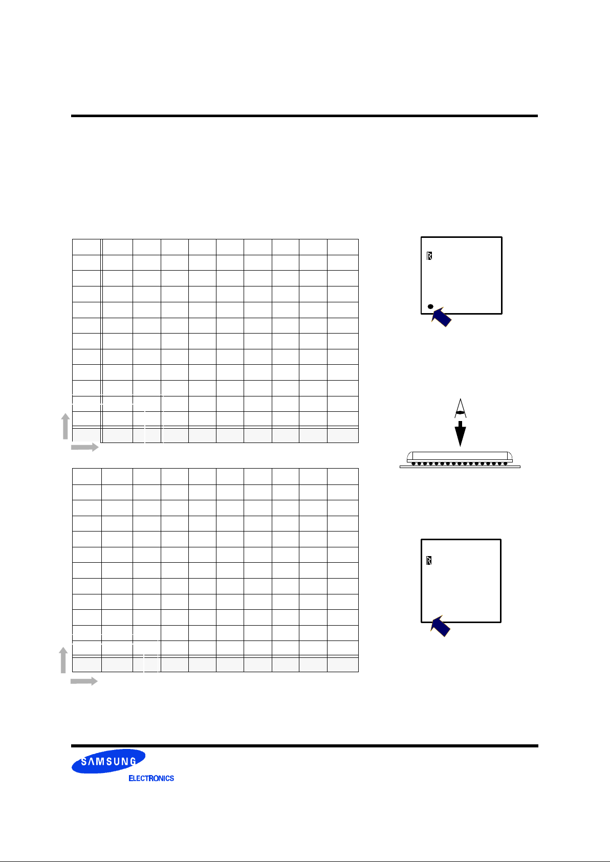
Table 1-1: a. Center-Bonded Device (top view for normal package)
12
GND VDD VDD GND
11
10
DQA7 DQA4 CFM CFMN RQ5 RQ3 DQB0 DQB4 DQB7
9
GND VDD GND GNDa VDD GND VDD VDD GND
8
CMD DQA5 DQA2 VDDa RQ6 RQ2 DQB1 DQB5 SIO1
7
6
5
SCK DQA6 DQA1 VREF RQ7 RQ1 DQB2 DQB6 SIO0
4
VCMOS GND VDD GND GND VDD GND GND VCMOS
3
DQA8* DQA3 DQA0 CTMN CTM RQ4 RQ0 DQB3 DQB8*
2
1
GND VDD VDD GND
A B C D E F G H J
Table 1-2: a. Center-Bonded Device (top view for mirrored package)
12
GND VDD VDD GND
11
10
DQA8* DQA3 DQA0 CTMN CTM RQ4 RQ0 DQB3 DQB8*
9
VCMOS GND VDD GND GND VDD GND GND VCMOS
8
SCK DQA6 DQA1 VREF RQ7 RQ1 DQB2 DQB6 SIO0
7
6
5
CMD DQA5 DQA2 VDDa RQ6 RQ2 DQB1 DQB5 SIO1
4
GND VDD GND GNDa VDD GND VDD VDD GND
3
DQA7 DQA4 CFM CFMN RQ5 RQ3 DQB0 DQB4 DQB7
2
1
GND VDD VDD GND
A B C D E F G H J
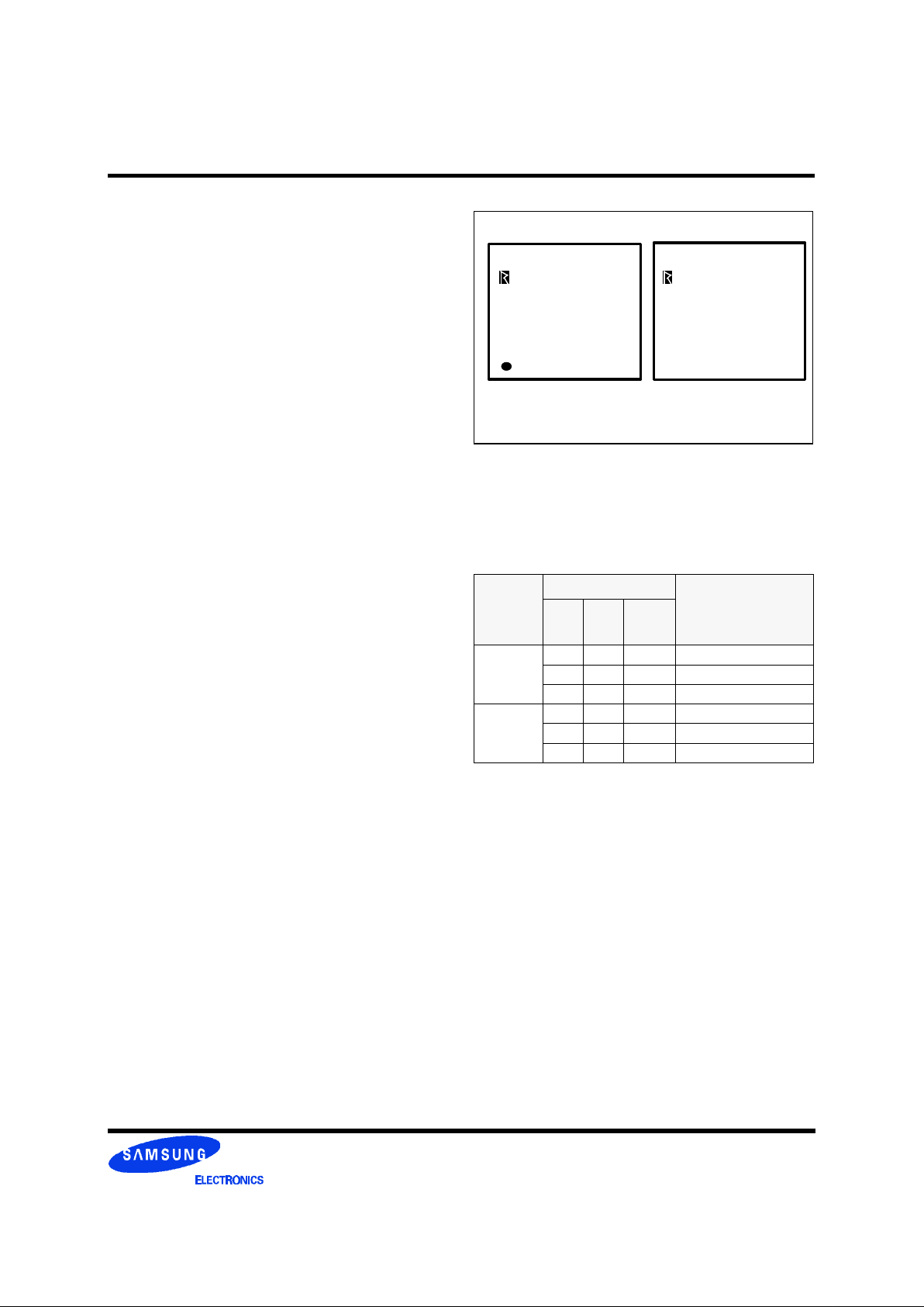
For normal package, pin #1(ROW 1, COL A) is
located at the A1 position on the top side and the A1
position is marked by the marker “•“.
For mirrored package, pin #1(ROW 1, COL A) is
located at the A1 postion on the top side and the A1
position is marked by the alphabet “M“.
Chip
Top View
* DQA8/DQB8 are just used for 144Mb RDRAM.
These two pins are NC(No Connection) in 128Mb
RDRAM.
b. Top marking example of normal package
b. Top marking example of mirrored package
COL
ROW
COL
ROW
K4Rxxxx69B-Nxxx
SAMSUNG 050
M
K4Rxxxx69B-Mxxx
SAMSUNG 050
Direct RDRAM
™
Page 3
K4R271669B/K4R441869B
Version 1.11 Oct. 2000
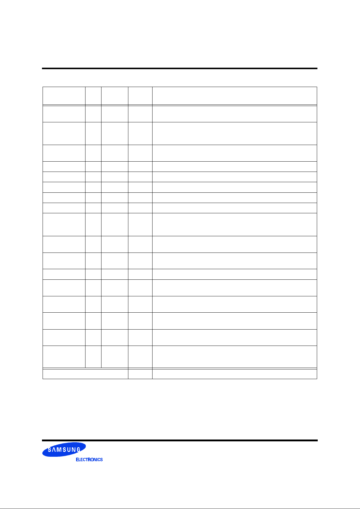
Table 2: Pin Description
Signal I/O Type
# of
Pins
Description
SIO1,SIO0 I/O CMOSa2 Serial input/output. Pins for reading from and writing to the control regis-
ters using a serial access protocol. Also used for power management.
CMD I CMOSa1 Command input. Pins used in conjunction with SIO0 and SIO1 for reading
from and writing to the control registers. Also used for power management.
SCK I CMOSa1 Serial clock input. Clock source used for reading from and writing to the
control registers
V
DD
10 Supply voltage for the RDRAM core and interface logic.
V
DDa
1 Supply voltage for the RDRAM analog circuitry.
V
CMOS
2 Supply voltage for CMOS input/output pins.
GND 13 Ground reference for RDRAM core and interface.
GNDa 1 Ground reference for RDRAM analog circuitry.
DQA8..DQA0 I/O RSL
b
9 Data byte A. Nine pins which carry a byte of read or write data between
the Channel and the RDRAM. DQA8 is not used (no connection) by
RDRAMs with a x16 organization.
CFM I RSL
b
1 Clock from master. Interface clock used for receiving RSL signals from
the Channel. Positive polarity.
CFMN I RSL
b
1 Clock from master. Interface clock used for receiving RSL signals from
the Channel. Negative polarity
V
REF
1 Logic threshold reference voltage for RSL signals
CTMN I RSL
b
1 Clock to master. Interface clock used for transmitting RSL signals to the
Channel. Negative polarity.
CTM I RSL
b
1 Clock to master. Interface clock used for transmitting RSL signals to the
Channel. Positive polarity.
RQ7..RQ5 or
ROW2..ROW0
I RSL
b
3 Row access control. Three pins containing control and address informa-
tion for row accesses.
RQ4..RQ0 or
COL4..COL0
I RSL
b
5 Column access control. Five pins containing control and address informa-
tion for column accesses.
DQB8..
DQB0
I/O RSL
b
9 Data byte B. Nine pins which carry a byte of read or write data between
the Channel and the RDRAM. DQB8 is not used (no connection) by
RDRAMs with a x16 organization.
Total pin count per package 62
a. All CMOS signals are high-true; a high voltage is a logic one and a low voltage is logic zero.
b. All RSL signals are low-true; a low voltage is a logic one and a high voltage is logic zero.
Direct RDRAM
™
Page 4
K4R271669B/K4R441869B
Version 1.11 Oct. 2000
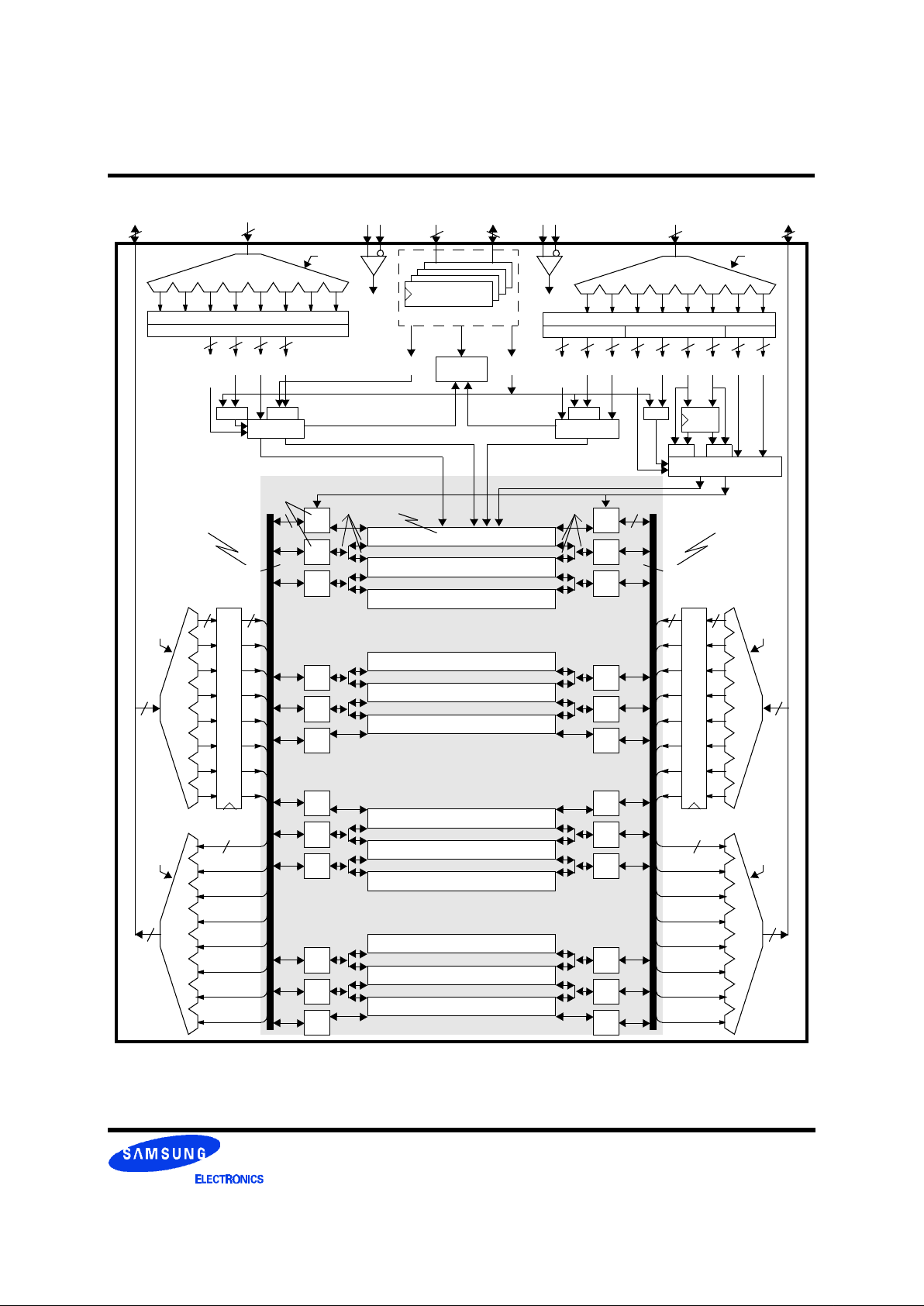
Figure 2: 128/144 Mbit(256K x16/18 x32s) Direct RDRAM Block Diagram
Bank 31
DQA8..DQA0
1:8 Demux8:1 Mux
Write Buffer
1:8 Demux
Write Buffer
8:1 Mux
Bank 30
Bank 29
Bank 18
Bank 17
Bank 16
Bank 15
Bank 14
Bank 13
Bank 1
Bank 0
SAmp
1/2
DQB8..DQB0
9
1:8 Demux
1:8 Demux
Packet Decode
95
3
ROW2..ROW0 COL4..COL0CTM CTMN CFM CFMN
2
SCK,CMD
RCLKTCLK
Control Registers
DCCOP CBC MAMBDXXOP BXDR RROP BR
886555556
95511
AV M S
Write
Buffer
Match
Match
Mux
Match
DEVID
512x64x144
Internal DQB Data Path
Column Decode & Mask
72
9
9
72
9
DM
REFR
Row Decode
Mux
ACT
RD, WR
Power Modes
DRAM Core
Mux
XOP Decode
PREX
PREC
9 99
9
72
9
9 9
PRER
COLX COLC COLM
2
SIO0,SIO1
Sense Amp
Internal DQA Data Path
Packet Decode
ROWA ROWR
RCLK RCLK
RCLKTCLK
RCLK TCLK
RQ7..RQ5 or
RQ4..RQ0 or
SAmp
0/1
SAmp
0
SAmp
14/15
SAmp
15
SAmp
13/14
SAmp
16/17
SAmp
17/18
SAmp
16
SAmp
29/30
SAmp
30/31
SAmp
31
32x72
SAmp
1/2
72
SAmp
0/1
SAmp
0
SAmp
14/15
SAmp
15
SAmp
13/14
SAmp
16/17
SAmp
17/18
SAmp
16
SAmp
29/30
SAmp
30/31
SAmp
31
32x72
32x72
Bank 2
•••
•••
•••
•••
•••
•••
 Loading...