


Samsung Electronics 3-1
3. Troubleshooting
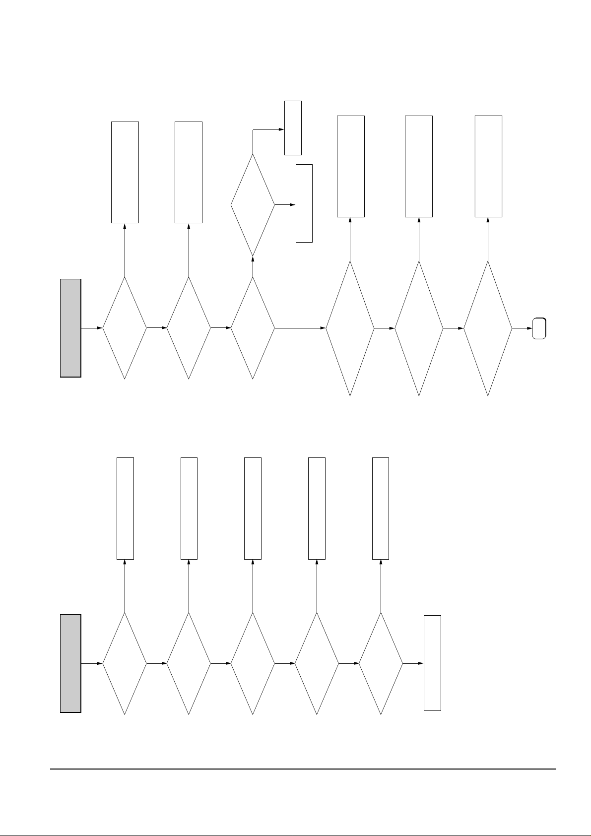
Loading error
PL11, PL13 voltage is O.K?
Check the power cable.
J4 (MAIN B/D)
Yes
No
Check the front cable.
J6 (MAIN B/D)
Check the 27M crystal.
MX1 (MAIN B/D)
R5 volage is 3.3V?
Yes
No
Clock signal on MR2?
Yes
No
Clock signal on R272,
R273, R274?
Check the RCKIO, U28.
Yes
No
Pulse signal on MR19,
R11, R12?
Check the MIC3, MIC4.
Yes
No
No disc in drive?
Retry without any disc.
Yes
No
Pulse signal on MIC1-8?
Check the EIC1 & resistors.
Yes
No
A
Endless pulse signal
on FIC1 - 13?
No
Yes
GND signal on MR20?
No
Yes
GND signal on FIC1 - 16?
No
Yes
GND signal on FR8?
Check the CIC5.
No
Yes
Check the U15 & resistors.
Check the U21.
Check the U21.
GND signal on FR7?
Check the CIC4.
No
Yes
GND signal on FR6?
Check the CIC1.
No
Yes
Replace the MIC1
A

Troubleshooting
3-2 Samsung Electronics
No Tray Open/Close
Turn off the power.
Shift down the front
door manually.
Open the drive tray manually
(using the drive switch)
Check the Drive power & Front
door power.
Tray open/close?
(Retry with no disc)
Retry with disc.
No
Yes
Loading error?
Check the Loading error procedure.
No
Yes
Tuner video input error
Normal 12C CLOCK
and DATA in JCN3-10,
11 (IO B/D)?
Normal 12C CLOCK
and DATA in TU1-10,
11 (IO B/D)?
Check the connection from
FIC1 (FRONT B/D)
Yes
No
Check the connection between
JCN3 and TU1 (IO B/D)
Check Powers in TU1 (IO B/D)
(pin13 : 5V Pin15 : 33V)
Check the connection between
TU1 and VIC1 (IO B/D)
Check the connection between
TU1 and TIC4 (IO B/D)
Check Sync separation part
(IO B/D) (TIC4, TQ1, TIC2)
Check the connection between
TIC2 (IO B/D) and FIC1 (FRONT B/D)
Yes
No
Normal CVBS signal
in TU1-21 (IO B/D)?
Yes
No
Normal CVBS signal
in VIC1-3 (IO B/D)?
Yes
No
Normal CVBS signal
in TIC4-1 (IO B/D)?
Yes
No
TR17 is High level (IO B/D)?
Yes
No
FIC1-33 is High level
(FRONT B/D)?
Yes
No
B

Troubleshooting
Samsung Electronics 3-3
Normal Video signal
in VIC1-4 (IO B/D)?
Yes
No
Normal Video data in
VIC1-81-90 (MAIN B/D)?
Yes
No
Normal Video data in
TIC2-64-71 (MAIN B/D)?
Normal Video data in
U21-201-208 (MAIN B/D)?
Yes
No
Normal clock in U21-200
(MAIN B/D)?
Yes
No
Yes
No
Normal digital signal
U21-68-178 (MAIN B/D)?
Yes
No
Replace the U21
H
Check the VIC1 (IO B/D)
(Pin6 = 'L' level)
Check the VIC1 (MAIN B/D)
(Clock, Power)
Check the TIC2 (MAIN B/D)
(Clock, Power)
Check the connection between
TIC2 and U21 (MAIN B/D)
Check the connection between
IC1 and U21 (MAIN B/D)
Check the connection between
MIC1 and U21 (MAIN B/D)
B
Tuner audio input error
Tuner video bypass is O.K?
Check the Tuner Video input
error procedure.
Yes
No
Repalce the TU1.
Check the TIC1 (IO B/D)
(Clock, Power)
Check the connection between
TIC1 and AIC1 (IO B/D)
Normal Audio signal in
TU1-18 (IO B/O)?
Yes
No
Normal Audio signal in
TIC1-36, 37 (IO B/O)?
Yes
No
Normal Audio signal in
AIC1-12, 1 (IO B/O)?
Yes
No
C

Troubleshooting
3-4 Samsung Electronics
Digital output error
(Playback)
Analog Audio output is O.K?
Check the L/R output
error procedure
Yes
No
Check U18
Check the connection between
U23 and AIC5
Check the Power of the
AIC5 pin 14 : 5V
Check the connection between
AIC5 and Jacks
Check the connection between
U18 and U23
Check the U23-1 -> 'H' state
Normal digital
data in U18-127
(MAIN B/D)?
Yes
No
Normal digital
data in U23-4
(MAIN B/D)?
Yes
No
Normal digital
data in AIC5-13 (IO B/D)?
Yes
No
Normal digital
data in AIC5-6 (IO B/D)?
Yes
No
Normal digital
data in AJ1, AJ2 (IO B/D)?
Yes
No
Check the cable
D
Digital output error
(Bypass)
Analog Audio output is O.K?
Go to the L/R output error
Yes
No
Check U21
Check the connection between
U21 and U23
Normal digital
data in U21-97
(MAIN B/D)?
Yes
No
Normal digital
data in U23-2
(MAIN B/D)?
Yes
No
D
Troubleshooting
Samsung Electronics 3-5
No Power (Standly LED off)
F01 is O.K?
Yes
No
D1 voltage is O.K?
Yes
No
IC1 drain(pin1)
voltage is O.K?
Yes
No
Voltage exists in IC1-5?
Yes
No
Pulse is O.K in IC1-5?
Yes
No
Check feed back
Replace fuse
Check C7
Check 2nd voltage
Check PR21, PR22, PR23, PR24
Replace IC1
Y/Pb/Pr(480p) output error
Normal digital data
output in U21-71-78
(MAIN B/D)?
Check the U21
Yes
No
Check RP12 and RP13
Check 27MHz oscillation
and change PIC5
Check PRP11, PRP12, PRP9,
PRP10, PRP3, PRP5, PR42, PR32,
PR39, PR40, PR27, PR26
Check the control pins
PIC6-96, 97, 54, 55, 56
Normal digital data
input in PIC5-137-144
(MAIN B/D)?
Yes
No
Normal digital data
input in PIC5-1, 158, 160
(MAIN B/D)?
Yes
No
Normal digital data
input in PIC3-2, 3, 4
(MAIN B/D)?
Yes
No
Normal digital data
output in PIC5-15~27(Pb), 28~41(Pr),
43~56(Y) (MAIN B/D)?
Yes
No
Normal digital data
output in PIC5-15~27(Pb), 28~41(Pr),
43~56(Y) (MAIN B/D)?
Yes
No
Normal digital data
output in PIC5-15~27(Pb), 28~41(Pr),
43~56(Y) (MAIN B/D)?
Yes
No
Check PR44, PR46, PR47
Check the MIC1
E

Troubleshooting
3-6 Samsung Electronics
Check cables
Check PRP8, PRP6, PRP7,
PRP4, PRP2, PRP1, PR41, PR34,
PR31, PR30, PR29
Check the pin of PIC1
12, 13 : 5V
37 : about 1.0V
Check connection between
PIC1 (MAIN B/D) and VIC5 (IO B/D)
Normal digital data
input in PIC1-39~48(Pb), 14~23(Pr),
1~10(Y) (MAIN B/D)?
Yes
No
Normal video signal
output in PIC1-28(Pb), 34(Pr),
32(Y) (MAIN B/D)?
Yes
No
Normal video signal
input in VIC5-4(Pb), 2(Pr),
7(Y) (IO B/D)?
Yes
No
Check connection between
VIC5(IO B/D) and RCA jacks
Check power of VIC5 (IO B/D)
Normal video signal
output in VIC5-13(Pb), 15(Pr),
20(Y) (IO B/D)?
Yes
No
Normal video signal
in RCA jacks (R-JACK B/D)?
Yes
No
E
L/R output error
Normal Z_SOUT is
input in U24-10?
Normal DA_SIN is
input in AIC6-6?
Check ZIVA 4.1 - 121 OUTPUT
Yes
No
Check U24-9 OUTPUT
Check ZIVA 4.1 - 125
(CD/VCD : 16.9344MHz,
DVD : 18.432MHz)
Check AIC8A peripheral circuit
Check FIC1-51 AMUTE
Check LO12 peripheral
soldering shot
Yes
No
Analog output of
AIC6-20, 21, 22, 23 is
normal?
Yes
No
AIC8-1, 7 OUTPUT
is normal?
Yes
No
Base terminal level
of AD3, AD4 are "L"?
Yes
No

Troubleshooting
Samsung Electronics 3-7
Input1 Bypass Error
Normal analog is input
in AIC1-11, 4?
Yes
No
AIC1 output is input
in HIC2-3, 5?
Yes
No
Analog output of
AIC2, AIC3 are normal?
Yes
No
ADC_SOUT is input
in U16-9, 10?
Yes
No
U15-DATX0 is normal?
Yes
No
Check U21 T_SOUT
Check R-JACK LIN1, RIN1
Check AIC1-3, 13
Check HIC2-1, 7 output
Check AIC4-21 output
Check U16-8 output
C
Input2 Bypass Error
Normal analog is input
in AIC1-5, 14?
Yes
No
AIC1 output is input
in HIC2-3, 5?
Yes
No
Analog output of
AIC2, AIC3 are normal?
Yes
No
ADC_SOUT is input
in U16-9, 10?
Yes
No
U15-DATX0 is normal?
Yes
No
Check U21 T_SOUT
Check R-JACK LIN2, RIN2
Check AIC1-3, 13
Check HIC2-1, 7 output
Check AIC4-21 output
Check U16-8 output

Troubleshooting
3-8 Samsung Electronics
Input3 Bypass Error
Normal analog is input
in AIC1-2, 15?
Yes
No
AIC1 output is input
in HIC2-3, 5?
Yes
No
Analog output of
AIC2, AIC3 are normal?
Yes
No
ADC_SOUT is input
in U16-9, 10?
Yes
No
U15-DATX0 is normal?
Yes
No
Check U21 T_SOUT
Check F-JACK LIN3, RIN3
Check AIC1-3, 13
Check HIC2-1, 7 output
Check AIC4-21 output
Check U16-8 output
CVBS Output Error
Check the PIXOUT[7..0] in
U21(TL750)
Check the soldering of VU2
Change VU2
Check the connection between
Pin2/3 in CON5 & Q1P11
Check the normal output
at pin 82 in U21
Normal VOUT[7..0] is
input in VU2?
Yes
No
Pin of & VDD3.3 in SAA7128(VU2)
has normal level?
Yes
No
27MHz clock input is normal
at pin 4 in VU2?
Yes
No
Check the normal output pin 11
in MIC9 & pin 184/185 in
MIC1(SH7709)
RSTAV is high state at
pin 40 in VU2?
Yes
No
Analog signals Output
normally at pin
30, 29, 27, 26, 24, in VU2?
Yes
No
Check the connection between
CON31 & JCN5
Analog signals are Input
normally at pin 2, 4, 6, 9, 11, 13
in MM1540(VIC3)?
Yes
No
F

Troubleshooting
Samsung Electronics 3-9
Power is normal at
pin 1, 28 in VIC3?
Yes
No
Pin 7, 8 in VIC3 is in
low state?
Yes
No
P-P Voltage level of pin
27 in VIC3 is 2V?
Yes
No
Video signal of about 1V
appears at output jack?
Yes
No
Check the RCA Cable
Check the Voltage is 8V
at pin 1 in JCN4
Check the connection between
JCN2 & CN2
Connect to High
Check the soldering of VIC3
Change VU2
G
F
S-Video Output Error
Analog signals Output
normally at pin of 23, 25
in VIC3?
Analog signals Output
normally appears at output
jack?
Yes
No
Yes
No
Check the RCA Cable
G
Check the connection between
JCN2 & CN2
Check the soldering of VIC3
Change VU2

Troubleshooting
3-10 Samsung Electronics
Y,Pr,Pb(480i) Output Error
Analog signals Output
normally at pin of 16, 18, 20
in VIC3?
Analog signals Output
normally appears at output
jack?
Yes
No
Yes
No
Check the RCA Cable
G
Check the connection between
JCN2 & CN2
Check the soldering of VIC3
Change VU2
Y,Pr,Pb(480i) Output Error
Analog signals Output
normally at pin of 16, 18, 20
in VIC3?
Analog signals Output
normally appears at output
jack?
Yes
No
Yes
No
Check the RCA Cable
G
Check the connection between
JCN2 & CN2
Check the soldering of VIC3
Change VU2

Troubleshooting
Samsung Electronics 3-11
CVBS Input Error (INPUT 2)
Analog signals Input
normally appears at
CV_IN 2 in R-Jack?
Analog signals are Input
normally at pin 12 in EMC
Filter(VF2)?
Analog signals are Input
normally at pin 20 in
SAA7114(VIC1)?
Analog signals Input
normally at pin of 5 in VIC2?
Analog signals Output
normally at pin of 4 in VIC2?
Yes
No
Yes
No
Yes
No
Yes
No
Yes
No
Check the RCA Cable
Check the connection between
JCN2 & CN2
Check the pin of 9, 10, 11 in
VIC2 is LOW
Check the connection between
CON31 & JCN5
Check the soldering of VF2
H
CVBS Input Error (INPUT 3)
Analog signals Input
normally appears at
CV_IN 3 in R-Jack?
Analog signals are Input
normally at pin 12 in EMC
Filter(VF2)?
Analog signals are Input
normally at pin 20 in
SAA7114(VIC1)?
Analog signals Input
normally at pin of 3 in VIC2?
Analog signals Output
normally at pin of 4 in VIC2?
Yes
No
Yes
No
Yes
No
Yes
No
Yes
No
Check the RCA Cable
Check the connection between
JCN7 & TCN1
Check the pin of 9, 10, 11 in
VIC2 is HIGH
Check the connection between
CON31 & JCN5
Check the soldering of VF2
H

Troubleshooting
3-12 Samsung Electronics
S-Video Input Error (INPUT 1)
Analog signals Input
normally appears at
CV_IN 1 in R-Jack?
Analog signals are Input
normally at pin 20 in
SAA7114(VIC1)?
Analog signals Input
normally at pin of
2, 4 in JCN1?
Analog signals are Input
normally at pin 15, 12, in
EMC Filter(VF1)?
Yes
No
Yes
No
Yes
No
Yes
No
Check the RCA Cable
Check the connection between
JCN1 & CN1
Check the connection between
CON31 & JCN5
Check the soldering of VF1
H
S-Video Input Error (INPUT 2)
Analog signals Input
normally appears at
CV_IN 2 in R-Jack?
Analog signals are Input
normally at pin 20, 16 in
SAA7114(VIC1)?
Analog signals Input
normally at pin of
12, 2 in VIC2?
Output signals at pin of
14, 15 are input signals at pin
of 12, 2 in VIC2?
Yes
No
Yes
No
Yes
No
Yes
No
Check the RCA Cable
Check the connection between
JCN1 & CN1
Check the pin of 9, 10, 11 in
VIC2 is LOW
Analog signals are Input
normally at pin 18, 15 in
EMC Filter(VF2)?
Yes
No
Check the connection between
CON31 & JCN5
Check the soldering of VF2
H

Troubleshooting
Samsung Electronics 3-13
S-Video Input Error (INPUT 3)
Analog signals Input
normally appears at
CV_IN 3 in F-Jack?
Analog signals are Input
normally at pin 20, 16 in
SAA7114(VIC1)?
Analog signals Input
normally at pin of
3 in VIC2?
Output signals at pin of
14, 15 are input signals at pin
of 13, 1 in VIC2?
Yes
No
Yes
No
Yes
No
Yes
No
Check the RCA Cable
Check the connection between
JCN7 & TCN1
Check the pin of 9, 10, 11 in
VIC2 is HIGH
Analog signals are Input
normally at pin 18, 15 in
EMC Filter(VF2)?
Yes
No
Check the connection between
CON31 & JCN5
Check the soldering of VF2
H

Troubleshooting
3-14 Samsung Electronics
MEMO
 Loading...