

Page 1
<MOSFET>
<Di>
<MOSFET and Di>
1.5V Drive Nch+SBD MOSFET
ES6U2
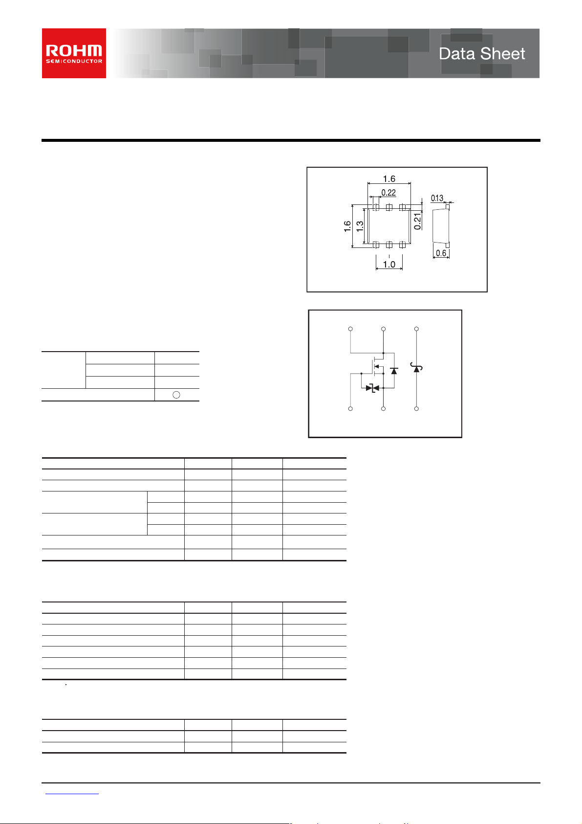
zStructure zDimensions (Unit : mm)
Silicon N-channel MOSFET /
Schottky barrier diode
zFeatures
1) Nch MOSFET and schottky barrier diode
are put in WEMT6 package.
2) High-speed switching, Low On-resistance.
3) Low voltage drive (1.5V drive).
4) Built-in Low VF schottky barrier diode.
zApplications zInner circuit
Switching
zPackage specifications
Type
ES6U2
Package
Code
Basic ordering unit (pieces)
Taping
T2R
8000
zAbsolute maximum ratings (Ta=25°C)
WEMT6
Abbriviated symbol : U02
(6)
∗1 ESD protection diode
∗2 Body diode
(1) (2)
(6) (5) (4)
(1) (2) (3)
(5)
∗2
∗1
(4)
(3)
(1)Gate
(2)Source
(3)Anode
(4)Cathode
(5)Drain
(6)Drain
Parameter
Drain-source voltage
Gate-source voltage
Drain current
Source current
(Body diode)
Continuous
Pulsed
Continuous
Pulsed
Channel temperature
Power dissipation W / ELEMENT0.7
∗1 Pw≤10µs, Duty cycle≤1%
∗2 Mounted on a ceramic board
Symbol
DSS
GSS
D
DP
S
SP
P
D
Limits Unit
20
±10
±1.5
∗1
±3.0
0.5
∗1
3.0
150
∗2
VV
VV
AI
AI
AI
AI
°CTch
Parameter
Repetitive peak reverse voltage
Reverse voltage
Forward current
Forward current surge peak
Junction temperature
Power dissipation W / ELEMENT
∗1 60Hz 1cyc.
∗2 Mounted on ceramic board
Symbol
RM
R
I
F
I
FSM
Tj
P
D
∗1
∗2
Limits Unit
25
20
0.5
2.0
150
VV
VV
A
A
°C
0.5
Parameter Symbol
Power dissipation
Range of storage temperature
∗ Mounted on a ceramic board
∗
D
Limits Unit
0.8
−55 to +150
W / TOTALP
°CTstg
www.rohm.com
1/5
c
○
2009 ROHM Co., Ltd. All rights reserved.
2009.12 - Rev.A
Page 2
<MOSFET>
<Body diode characteristics (Source-drain)>
<Di>
zElectrical characteristics (Ta=25°C)
Data Sheet ES6U2
Parameter Symbol
Gate-source leakage
Drain-source breakdown voltage
Zero gate voltage drain current
Gate threshold voltage
Static drain-source on-state
resistance
Forward transfer admittance
Input capacitance
Output capacitance
Reverse transfer capacitance
Turn-on delay time
Rise time
Turn-off delay time
Fall time
Total gate charge
Gate-source charge
Gate-drain charge
∗Pulsed
Parameter Symbol
∗Pulsed
I
V
(BR) DSS
I
V
GS (th)
R
DS (on)
C
C
C
t
d (on)
t
d (off)
Q
Q
V
Min.−Typ. Max.
GSS
−±10 µAVGS=±10V, VDS=0V
20 −−VI
DSS
−−1 µAV
0.3 − 1.0 V V
− 130 180 I
− 170 240 mΩ
∗
− 220 310 I
∗
1.6 −−SV
Y
fs
− 110 − pF V
iss
− 1815− pF V
oss
−
rss
∗
∗
t
r
∗
∗
t
f
∗
Q
g
∗
gs
∗
gd
5
−
5
−
20
−
3
−
1.8
−
0.3
−
0.3
−−nC
Min. Typ. Max.
∗
SD
−−1.2 V IS= 1.5A, VGS=0VForward voltage
Unit
= 1mA, VGS=0V
D
= 20V, VGS=0V
DS
= 10V, ID= 1mA
DS
= 1.5A, VGS= 4.5V
mΩ
D
= 1.5A, VGS= 2.5V
I
D
mΩ
= 0.8A, VGS= 1.8V
D
mΩ− 300 600 I
= 0.3A, VGS= 1.5V
D
= 10V, ID= 1.5A
DS
= 10V
DS
=0V
GS
− pF f=1MHz
− ns
− ns
− ns
− ns
− nC
− nC
VDD 10V
ID= 1A
GS
= 4.5V
V
L
10Ω
R
G
= 10Ω
R
V
10V, VGS= 4.5V
DD
ID= 1.5A, R
= 10Ω
R
G
Unit
Conditions
6.7Ω
L
Conditions
Parameter Symbol
Forward voltage
Reverse current
Min. Typ. Max.
F
R
I
−−
−−
−−
V
Unit
0.36 V
0.52 V
100
µA
= 0.1A
I
F
= 0.5A
I
F
= 20V
V
R
Conditions
www.rohm.com
2/5
c
○
2009 ROHM Co., Ltd. All rights reserved.
2009.12 - Rev.A
Page 3
V
V
V
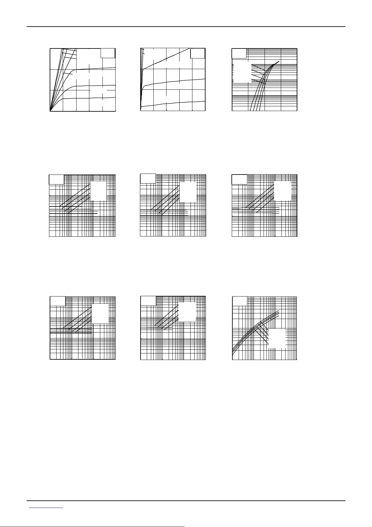
zElectrical characteristics curves
1.5
[A]
D
1
0.5
DRAIN CURRENT : I
0
0 0.2 0.4 0.6 0.8 1
VGS= 10
VGS= 4.5
VGS= 2.5
VGS= 1. 8V
VGS= 1.5V
VGS= 1.3V
VGS= 1. 2V
Ta=25°C
Pulsed
1.5
VGS= 4.5V
= 1.8V
V
GS
[A]
D
1
0.5
DRAIN CURRENT : I
0
0246810
VGS= 1. 5V
VGS= 1. 1V
VGS= 1.3V
Ta= 25°C
Pulsed
10
VDS= 10V
Pulsed
[A]
D
1
Ta= 125°C
Ta= 75°C
Ta= 25°C
Ta= - 25°C
0.1
DRAIN CURRENT : I
0.01
0.001
00.5 11.52
Data Sheet ES6U2
DR AIN-SOU RCE VOLTAGE : VDS[V] DR AIN-SOU RCE VOLTAGE : VDS[V]
Fi g.1 Typi cal Output C haract eris tics(Ⅰ) Fi g.2 T ypic al Output C haract eris tics(Ⅱ)
10000
Ta= 25°C
Pulsed
]
Ω
1000
(on)[m
DS
100
RESIST ANCE : R
STATIC DRAIN-SOURCE ON-STATE
10
0.01 0. 1 1 10
DRAIN-CURRENT : I
Fi g.4 Stati c Dr ain- Source On- State
Resi stance vs. D rain C urr ent(Ⅰ)
10000
VGS= 1. 8V
Pulsed
]
Ω
1000
(on)[m
DS
100
RESIST ANCE : R
STATIC DRAIN -SOUR CE ON- STATE
10
0.01 0.1 1 10
DRAIN-CURRENT : ID[A]
Fi g.7 Stati c Dr ain- Source On- State
Resistance vs. Dr ain Cur rent(Ⅳ)
VGS= 1.5V
= 1.8V
V
GS
V
= 2.5V
GS
= 4.5V
V
GS
[A]
D
Ta= 125°C
Ta= 75°C
Ta= 25°C
Ta= -25°C
10000
VGS= 4.5V
Pulsed
]
Ω
1000
(on) [m
DS
100
RESIST ANCE : R
STATIC DRAIN -SOUR CE ON- STATE
10
0.01 0.1 1 10
DRAIN-CURRENT : ID[A]
Fi g.5 Stat ic Dr ain- Source On- State
Resi stance vs. D rain C urr ent(Ⅱ)
10000
VGS= 1. 5V
Pulsed
]
Ω
1000
(on)[m
DS
100
RESIST ANCE : R
STATIC DRAIN -SOUR CE ON- STATE
10
0.01 0.1 1 10
DRAIN-CURRENT : ID[A]
Fi g.8 Stat ic Dr ain- Source On- State
Resi stance vs. D rain C urr ent(Ⅴ)
Ta= 125°C
Ta=75°C
Ta=25°C
Ta= -25°C
Ta= 125°C
Ta= 75°C
Ta= 25°C
Ta= -25°C
GATE- SOURCE VOLT AGE : VGS[V]
Fi g.3 T ypical Trans fer C haracter isti cs
10000
VGS= 2. 5V
Pulsed
]
Ω
1000
(on) [m
DS
100
RESIST ANCE : R
STATIC DRAIN -SOUR CE ON- STATE
10
0.01 0.1 1 10
DRAIN-CURRENT : ID[A]
Fi g.6 Stati c Dr ain- Source On- State
Resistance vs. Dr ain Cur rent(Ⅲ)
10
VDS= 10V
Pulsed
1
0.1
FOR WARD T RANSFER ADMITT ANCE : |Yfs | [S]
0.01 0.1 1 10
DRAIN-CURRENT : ID[A]
Fi g.9 F orward Tr ansfer Admittance
vs. Dr ain Curr ent
Ta=125°C
Ta=75°C
Ta=25°C
Ta= -25°C
Ta= -25°C
Ta=25°C
Ta=75°C
Ta=125°C
www.rohm.com
3/5
c
○
2009 ROHM Co., Ltd. All rights reserved.
2009.12 - Rev.A
Page 4
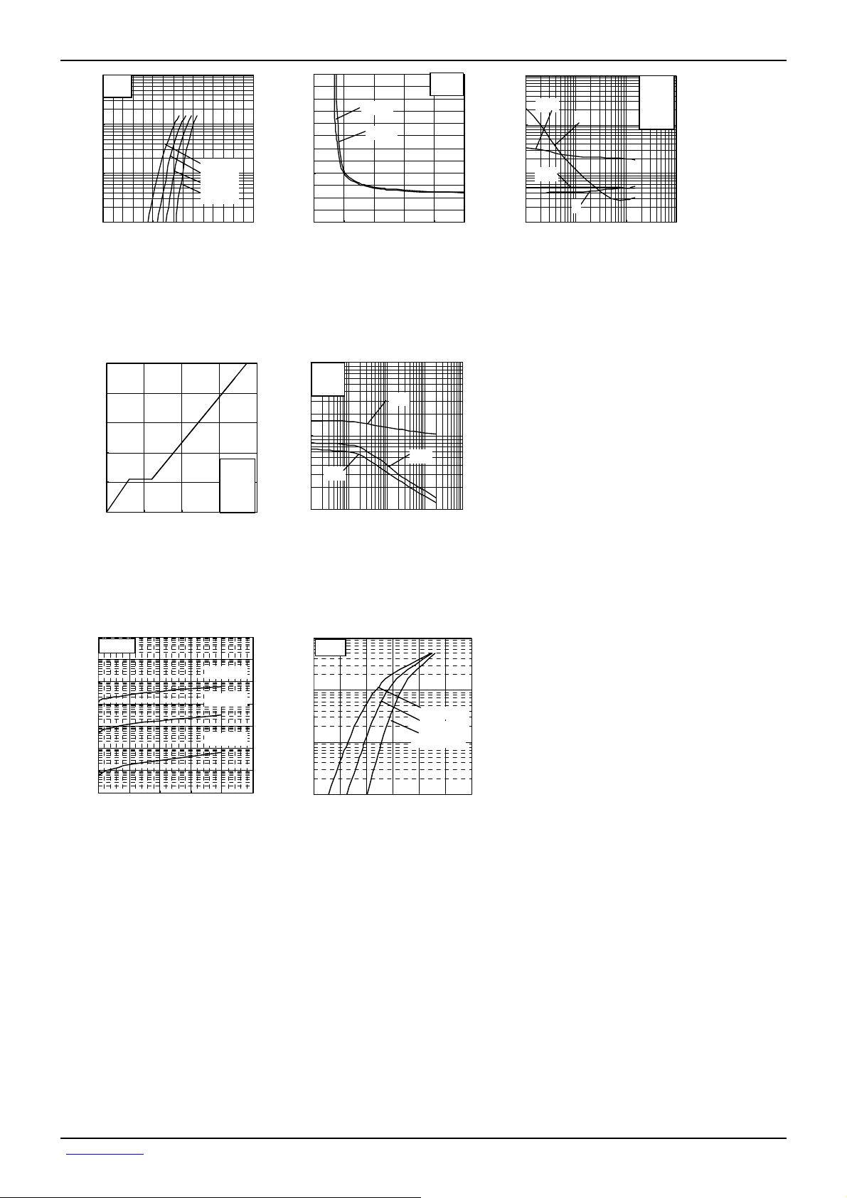
10
<Di>
VGS=0V
Pulsed
1
0.1
REVER SE DRAIN CURR ENT : Is [A]
0.01
0 0.5 1 1.5
SOURCE-DRAIN VOLTAGE : VSD [V]
Fi g.10 R evers e Drai n Curr ent
vs. Sours e-D rain Voltage
5
[V]
GS
4
3
2
1
GATE-SOU RCE VOLTAGE : V
0
00.511.52
TOTAL GATE CHARGE : Qg [nC] DRAIN-SOURCE VOLTAGE : VDS[V]
Fi g.13 D ynamic I nput Char acteri stic s Fi g.14 T ypical Capaci tance
100000
puls ed
10000
(A)
R
1000
100
10
1
REVERSE CURRENT : I
0.1
0.01
0 5 10 15 20 25
REVER SE VOLTAGE : VR[V]
Fig.1 Reverse Current vs. Reverse Voltage
Ta= 125°C
Ta= 75°C
Ta= 25°C
Ta= -25°C
Ta= 25°C
V
I
D
R
Pulsed
Ta = 75
Ta = 25
Ta= - 25
= 10V
DD
= 1. 5A
=10Ω
G
Data Sheet ES6U2
600
]
500
Ω
400
(ON)[m
DS
300
200
RESIST ANCE : R
100
STATIC DRAIN-SOURCE ON-STATE
0
0246810
Fi g.11 Stat ic D rain- Source On- State
Resis tance vs. Gate Source Voltag e
1000
Ta= 25°C
f=1MH z
V
GS
100
CAPACITANCE : C [pF]
10
0.01 0.1 1 10 100
1
pulsed
℃
℃
℃
(A)
F
0.1
0.01
FORWARD CURRENT : I
0.001
0 0.1 0. 2 0.3 0. 4 0.5 0.6
ID= 0. 8A
ID= 1.5A
GATE-SOU RCE VOLTAGE : VGS[V]
=0V
Crss
vs. Drain- Source Voltag e
FOR WARD VOLTAGE : V
Fi g.2 For ward C urrent vs. F orward Volt age
Ciss
Coss
Ta = 75
Ta = 25
Ta= - 25
Ta= 25°C
Pulsed
℃
℃
[V]
F
℃
1000
td(off)
t
100
10
td(on)
SWITC HING TIM E : t [ns]
1
0.01 0.1 1 10
f
t
r
DRAIN-CURRENT : ID[A]
Fi g.12 Swi tching Chara cteri stic s
Ta= 25°C
V
= 10V
DD
V
=4.5V
GS
=10Ω
R
G
Pulsed
www.rohm.com
4/5
c
○
2009 ROHM Co., Ltd. All rights reserved.
2009.12 - Rev.A
Page 5
F
it
%
V
V
F
it
S
FIg.2-2 Gate Charge Waveform
V
Data Sheet ES6U2
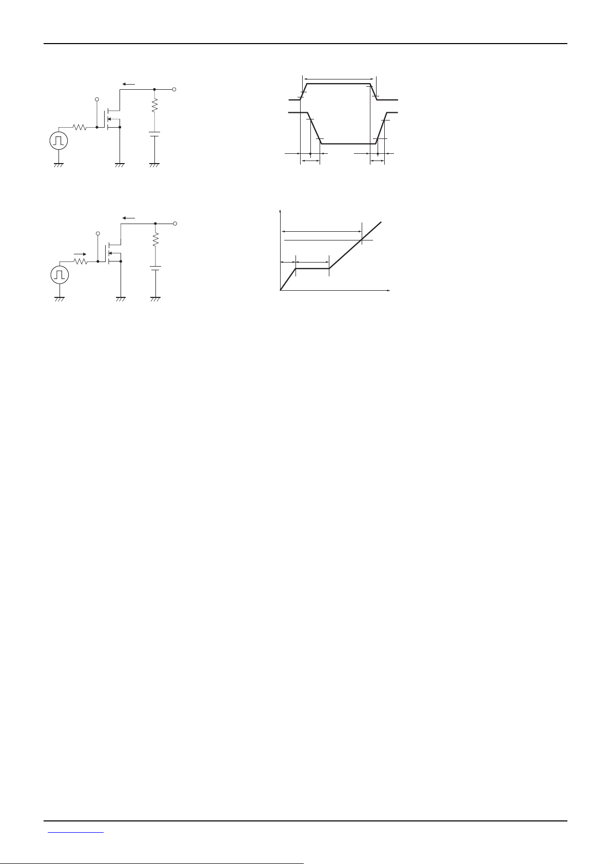
zMeasurement circuit
Pulse Width
D
V
GS
R
G
I
D.U.T.
V
DS
R
L
V
DD
ig.1-1 Switching Time Measurement Circu
50%
10%
GS
DS
t
d(on)
10%
t
on
Fig.1-2 Switching Waveforms
90%
t
r
90%
d(off)
t
t
50%
10
90%
tf
off
V
G
I
D
D.U.T.
I
G(Const.)
V
GS
R
G
ig.2-1 Gate Charge Measurement Circu
V
D
R
L
V
DD
GS
Q
gs
g
Q
Q
gd
Charge
zNotice
1. SBD has a large reverse leak current compared to other type of diode. Therefore; it would raise a junction temperature, and
increase a reverse power loss. Further rise of inside temperature would cause a thermal runaway.
This built-in SBD has low V
F characteristics and therefore, higher leak current. Please consider enough the surrounding
temperature, generating heat of MOSFET and the reverse current.
2. This product might cause chip aging and breakdown under the large electrified environment. Please consider to design ESD
protection circuit.
www.rohm.com
5/5
c
○
2009 ROHM Co., Ltd. All rights reserved.
2009.12 - Rev.A
Page 6

Notes
No copying or reproduction of this document, in part or in whole, is permitted without the
consent of ROHM Co.,Ltd.
The content specied herein is subject to change for improvement without notice.
The content specied herein is for the purpose of introducing ROHM's products (hereinafter
"Products"). If you wish to use any such Product, please be sure to refer to the specications,
which can be obtained from ROHM upon request.
Examples of application circuits, circuit constants and any other information contained herein
illustrate the standard usage and operations of the Products. The peripheral conditions must
be taken into account when designing circuits for mass production.
Great care was taken in ensuring the accuracy of the information specied in this document.
However, should you incur any damage arising from any inaccuracy or misprint of such
information, ROHM shall bear no responsibility for such damage.
The technical information specied herein is intended only to show the typical functions of and
examples of application circuits for the Products. ROHM does not grant you, explicitly or
implicitly, any license to use or exercise intellectual property or other rights held by ROHM and
other par ties. ROHM shall bear no responsibility whatsoever for any dispute arising from the
use of such technical information.
Notice
The Products specied in this document are intended to be used with general-use electronic
equipment or devices (such as audio visual equipment, ofce-automation equipment, communication devices, electronic appliances and amusement devices).
The Products specied in this document are not designed to be radiation tolerant.
While ROHM always makes efforts to enhance the quality and reliability of its Products, a
Product may fail or malfunction for a variety of reasons.
Please be sure to implement in your equipment using the Products safety measures to guard
against the possibility of physical injury, re or any other damage caused in the event of the
failure of any Product, such as derating, redundancy, re control and fail-safe designs. ROHM
shall bear no responsibility whatsoever for your use of any Product outside of the prescribed
scope or not in accordance with the instruction manual.
The Products are not designed or manufactured to be used with any equipment, device or
system which requires an extremely high level of reliability the failure or malfunction of which
may result in a direct threat to human life or create a risk of human injury (such as a medical
instrument, transportation equipment, aerospace machiner y, nuclear-reactor controller,
fuel-controller or other safety device). ROHM shall bear no responsibility in any way for use of
any of the Products for the above special purposes. If a Product is intended to be used for any
such special purpose, please contact a ROHM sales representative before purchasing.
If you intend to export or ship overseas any Product or technology specied herein that may
be controlled under the Foreign Exchange and the Foreign Trade Law, you will be required to
obtain a license or permit under the Law.
Thank you for your accessing to ROHM product informations.
More detail product informations and catalogs are available, please contact us.
ROHM Customer Support System
www.rohm.com
© 2009 ROHM Co., Ltd. All rights reserved.
http://www.rohm.com/contact/
R0039
A
 Loading...