


RT8208A/B
Programmable Output Voltage Single Synchronous
Buck Controller
General Description
The RT8208A/B is a constant-on-time PWM controller
which provides four resistor programmable DC output
voltages by controlling the G0 and G1 digital input. The
output voltage is programmable from 0.75V to 3.3V. The
RT8208A/B offers the lowest total solution cost in systems
where need output voltage slewing. The RT8208A/B
provides an automatic masking power good output during
output voltage transition.
The constant-on-time PWM control scheme handles wide
input/output ratios with ease and provides 100ns “instant-
on” response to load transient while maintaining a
relatively constant frequency. It provides the high efficiency,
excellent transient response, and DC output accuracy
needed for stepping down high voltage batteries to
generate low voltage CPU core, graphics, I/O and chipset
RAM supplies in notebook computers.
The RT8208A/B achieves high efficiency at a reduced cost
by eliminating the current sense resistor in traditional
current mode PWMs. Efficiency is further enhanced by
its ability to drive very large synchronous rectifier
MOSFETs. The buck conversion allows this device to
directly step down from high voltage batteries for the highest
possible efficiency. Additional features include soft-start,
under voltage protection, programmable over current
protection and non-overlapping gate drive. The RT8208A/
B is available in a WQFN-16L 3x3 package.
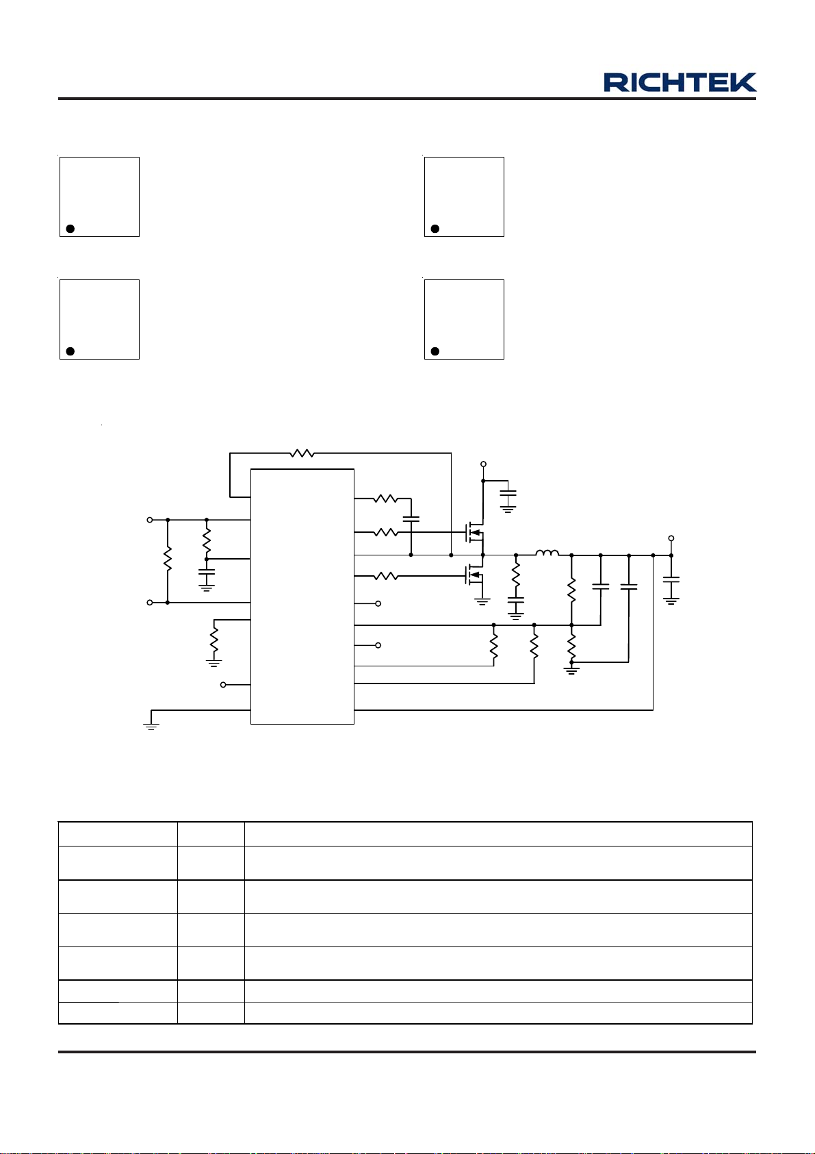
Pin Configurations
(TOP VIEW)
TON
EN/DEM
BOOT
G1
13141516
VOUT
VDD
FB
PGOOD
1
2
GND
3
4
D1G0D0
WQFN-16L 3x3
12
UGATE
11
PHASE
10
CS
17
9
VDDP
8765
LGATE
Features
zz
z Ultra-High Efficiency
zz
zz
z Resistor Progra mma ble Output Voltage from 0.75V
zz
to 3.3V with Integrated Transition Support
zz
z Quick Load Step Response within 100ns
zz
zz
z 1% V
zz
zz
z 4.5V to 26V Battery Input Range
zz
zz
z Resistor Programmable Frequency
zz
zz
z Integrated Bootstrap Switch
zz
zz
z Resistor Programmable Positive Current Limit by
zz
Low Side R
zz
z Negative Current Limiter
zz
zz
z Voltage Transient Overshoot Eliminator*
zz
zz
z Over Voltage Protection
zz
zz
z Under Voltage Protection
zz
zz
z 4 Steps Current Limit During Soft-Start
zz
zz
z Power Good Indicator
zz
zz
z RoHS Compliant and Halogen Free
zz
* Paten Pending
Accuracy over Line and Load
FB
Sense (Lossless Limit)
DS(ON)
Applications
z Notebook Computers
z System Power Supplies
z I/O Supplies
z Programmable-Output Power Supplies
Ordering Information
RT8208
Package Type
QW : WQFN-16L 3x3 (W-Type)
Lead Plating System
G : Green (Halogen Free and Pb Free)
Z : ECO (Ecological Element with
Halogen Free and Pb free)
Turn-on D0/D1 MOSFET
A : G0/G1 High
Note :
Richtek products are :
` RoHS compliant and compatible with the current require-
ments of IPC/JEDEC J-STD-020.
` Suitable for use in SnPb or Pb-free soldering processes.
B : G0/G1 Low
DS8208A/B-04 May 2011 www.richtek.com
1
RT8208A/B
Marking Information
RT8208AGQW
FF= : Product Code
FF=YM
DNN
YMDNN : Date Code
RT8208BGQW
FG=YM
DNN
FG= : Product Code
YMDNN : Date Code
RT8208AZQW
FF : Product Code
FF YM
YMDNN : Date Code
DNN
Typical Application Circuit
R
2
RT8208A/B
1
6
T
O
N
9
V
D
D
2
4
0
5
d
)
P
D
V
D
O
P
G
O
C
S
EN/DEM
D
N
G
D
D
P
D
V
1
R
1
0
2
R
1
0
0
k
2
C
1
µ
F
D
O
G
O
P
D
/
M
C
C
1
E
7
(
p
x
1
6
R
1
8
k
1
M
E
o
e
s
d
P
a
RT8208BZQW
FG : Product Code
FG YM
YMDNN : Date Code
DNN
3
0
5
k
4
R
0
1
B
G
U
P
H
L
G
V
3
O
O
T
C
5
R
0
1
2
A
T
E
1
1
A
S
E
R
1
8
A
T
E
0
7
G
F
B
G
D
D
O
U
T
G
0
3
1
4
G
1
5
1
6
0
1
3
0
1
.
0
B
S
C
1
0
1
V
N
I
4
5
.
o
t
V
2
6
V
4
C
1
0
µ
F
1
µ
F
1
9
Q
B
S
C
1
1
9
N
0
3
S
L
1
1
µ
H
R
Q
N
0
3
S
7
2
C
7
R
1
1
*
R
8
1
2
k
R
R
9
1
2
*
6
0
k
V
=
0
9
.
V
T
U
O
C
C
5
*
C
6
*
1
2
2
0
µ
F
*
O
p
:
a
o
l
i
n
t
Functional Pin Description
Pin No. Pin Name Pin Function
1 VOUT
2 VDD
3 FB
4 PGOOD
5 D1 Drain of the internal MOSFET which is controlled by G1.
6 D0 Drain of the internal MOSFET which is controlled by G0.
2
Output Voltage Pin. Connect to the output of PWM converter. VOUT is an input of
the PWM controller.
Analog supply voltage input for the internal analog integrated circuit. Bypass to
GND with a 1μF ceramic capacitor.
Feedback Input Pin. Connect FB to a resistor voltage divider from VOUT to GND
to adjust output voltage from 0.75V to 3.3V
Power good signal open-drain output of PWM converter. This pin will be pulled
high when the output voltage is within the target range.
To be continued
DS8208A/B-04 May 2011www.richtek.com

Pin No. Pin Name Pin Function
7 G0
8 LGATE
9 VDDP
10 CS
11 PHASE
12 UGATE
13 BOOT
14 G1
15 EN/DEM
16 TON
17 (Exposed pad) GND
Control Input Pin for the D0 MOSFET. A logic high for RT8208A and low for
RT8208B turn on the D0 MOSFET on, pulling D0 to the ground.
Low side N-MOSFET gate driver output for PWM. This pin swings between GND
and VDDP.
VDDP is the gate driver supply for external MOSFETs. Bypass to GND with a 1μF
ceramic capacitor.
Over Current Trip Point Set Input. Connect a resistor from this pin to signal ground
to set threshold for both over c urrent and negative over current limit.
The UGATE High Side Gate Driver Return. Also serves as anode of over current
comparator.
High side N-MOSFET floating gate driver output for the PWM converter. This pin
swings between PHASE and BOOT.
Boost Capacitor Connec tion for PWM Converter. Connect to an external ceramic
capacitor to PHASE.
Control Input Pin for the D1 MOSFET. A logic high for RT8208A and low for
RT8208B turn on the D1 MOSFET on, pulling D1 to the ground.
Enable/Diode Emulation Mode Control Input. Connect to VDD for diode–emulation
mode, connect to GND for shutdown and floating the pin for CCM mode.
On Time/Frequency Adjustment Pin. Connect to PHASE through a resistor. TON is
an input for the PWM controller.
The exposed pad must be soldered to a large PCB and connected to GND for
maximum power dissipation.
Function Block Diagram
RT8208A/B
VOUT
TON
FB
SS
(internal)
125% V
70% V
Blanking Signal
Counter
EN
G0, G1
-
GM
+
0.75V V
REF
REF
TRIG
On-time
Compute
1-SHOT
REF
+
-
+
-
90% V
SS Timer
OV
UV
REF
+
R
Latch
SQ
R
Latch
SQ
+
Thermal
Shutdown
G0 G1 D0 D1
Control
Logic
R
QS
Min. T
OFF
QTRIG
1-SHOT
Diode
Emulation
BOOT
DRV
DRV
10µA
+
+
-
GM
-
UGATE
PHASE
VDDP
LGATE
GND
CS
VDD
PGOOD
EN
DS8208A/B-04 May 2011 www.richtek.com
3

RT8208A/B
Absolute Maximum Ratings (Note 1)
z BOOT to GND -------------------------------------------------------------------------------------------------------------- −0.3V to 38V
z BOOT to PHASE ---------------------------------------------------------------------------------------------------------- −0.3V to 6V
z PHASE to GND
DC----------------------------------------------------------------------------------------------------------------------------- –0.3V to 32V
< 20ns ----------------------------------------------------------------------------------------------------------------------- −8V to 38V
z UGATE to PHASE
DC----------------------------------------------------------------------------------------------------------------------------- –0.3V to 6V
< 20ns ----------------------------------------------------------------------------------------------------------------------- −5V to 7.5V
z LGATE to GND
DC----------------------------------------------------------------------------------------------------------------------------- –0.3V to 6
< 20ns ----------------------------------------------------------------------------------------------------------------------- −2.5V to 7.5V
z VDD, VDDP, VOUT, EN/DEM, FB, PGOOD, TON to GND------------------------------------------------------- −0.3V to 6V
z CS to GND ------------------------------------------------------------------------------------------------------------------ −0.3V to 6V
z Power Dissipation, P
WQFN−16L 3x3 ------------------------------------------------------------------------------------------------------------ 1.471W
z Package Thermal Resistance (Note 2)
WQFN−16L 3x3, θJA------------------------------------------------------------------------------------------------------ 68°C/W
WQFN−16L 3x3, θJC------------------------------------------------------------------------------------------------------ 7.5°C/W
z Lead Temperature (Soldering, 10 sec.) ------------------------------------------------------------------------------- 260°C
z Junction Temperature ----------------------------------------------------------------------------------------------------- 150°C
z Storage Temperature Range -------------------------------------------------------------------------------------------- −65°C to 150°C
z ESD Susceptibility (Note 3)
HBM (Human Body Mode) ---------------------------------------------------------------------------------------------- 2kV
MM (Machine Mode) ------------------------------------------------------------------------------------------------------ 200V
@ T
D
= 25°C
A
Recommended Operating Conditions (Note 4)
z Input Voltage, V
z Supply Voltage, V
z Junction Temperature Range-------------------------------------------------------------------------------------------- −40°C to 125°C
z Ambient Temperature Range--------------------------------------------------------------------------------------------
---------------------------------------------------------------------------------------------------------- 4.5V to 26V
IN
, V
DD
---------------------------------------------------------------------------------------------- 4.5V to 5.5V
DDP
−40°C to 85°C
Electrical Characteristics
(V
= 15V, V
IN
PWM Con tro ll e r
Quiescent Supply Current IQ VDD + VDDP, VFB = 0.8V -- -- 1250 μA
Shutdown Current I
FB Reference Voltage V
FB Input Bias Current VFB = 0.75V −1 0.1 1 μA
Output Voltage Range V
4
= V
DD
= 5V, TA = 25°C, unless otherwise specified)
DDP
Parameter Symbol Test Conditions Min Typ Max Unit
SHDN
VDD = 4.5V to 5.5V 0.742 0.750 0.758 V
REF
0.75 -- 3.3 V
OUT
EN/DEM = GND −10 −1 --
VDD + V
-- 1 10
DDP
μA
To be continued
DS8208A/B-04 May 2011www.richtek.com

RT8208A/B
Parameter Symbol Test Conditions Min Typ Max Unit
D0 Pull-Down Resistance D0 to GND, G0 = 5V -- 10 -- Ω
D1 Pull-Down Resistance D1 to GND, G1 = 5V -- 10 --
PHASE
= 250kΩ
TON
= 12V, V
On-Time
V
R
= 2.5V,
OUT
336 420 504 ns
Minimum Off-Time 250 400 550 ns
VOUT Shutdown Discharge
Resistance
EN/D EM = GND -- 20 -- Ω
Curren t Sens ing
Current Limiter Source Current CS to GND 9 10 11 μA
Current Comparator Offset −10 -- 10 mV
Zero Crossing Threshold PHASE to GND, EN/DEM = 5V −10 -- 5 mV
Fault Protection
Ω
Current Limit (Threshold)
GND to PHASE, V
= 200mV 190 200 210
CS
mV
Current Limit Setting Range CS to GND 50 -- 200 mV
Output UV Threshold UVP Detection 60 70 80 %
GND to PHASE, VCS = 50mV 40 50 60
OVP Threshold V
FB_OVP
OVP Detection 120 125 130 %
OV Fault Delay FB forced above OV threshold -- 20 -- μs
VDD Under Voltage Lockout
Threshold
Current Limit Step Duration at
Soft-Start
Rising edge, PWM disabled below
this level
Hysteresis -- 80 -- mV
Each step -- 128 -- clks
4.1 4.3 4.5 V
UVP Blanking Time From EN signal going high -- 512 -- clks
Thermal Shutdown T
-- 155 -- °C
SH DN
Thermal Shutdown Hysteresis -- 10 -- °C
Dri ver On-Resis ta nce
UGATE Drive Source R
UGATE Drive Sink R
LGATE Drive Source R
LGATE Drive Sink R
UGATE Gate Driver Source/Sink
Current
LGATE Gate Driver Source
Current
UGATEsr
UGATEsk
LGATEsr
LGATEsk
LGATE forced to 2.5V -- 1 -- A
BOOT to PHASE = 5V -- 2 5 Ω
BOOT to PHASE = 5V -- 1 5
Ω
LGATE, High State -- 1 5 Ω
LGATE, Low State -- 0.5 2.5
UGATE to PHASE = 2.5V,
BOOT to PHASE = 5V
-- 1 -- A
Ω
LGATE Gate Driver Sink Current LGATE forced to 2.5V -- 3 -- A
Dead Time
LGATE Rising (Phase = 1.5V) -- 30 --
ns
UGATE Rising -- 30 --
Internal Boost Charging Switch
On-Resistance
VDDP to BOOT, 10mA -- -- 80 Ω
To be continued
DS8208A/B-04 May 2011 www.richtek.com
5

RT8208A/B
Parameter Symbol Test Conditions Min Typ Max Unit
Logic I/O
EN/DEM Low -- -- 0.8
EN/DEM Logic Input Voltage
EN/DEM H igh 2.9 -- --
V
EN/DEM Floating -- 2 --
G0 Logic Input Voltage
G0 Low -- -- 0.8
V
G0 High 2 -- --
G1 Logic Input Voltage
G1 Low -- -- 0.8
V
G1 High 2 -- --
EN/DEM = VDD -- 1 5
EN/DEM = 0 −5 1 -- Logic Input Current
μA
G0 = G1 = VDD or GND −1 -- 5
PGOOD
with respec t to Referenc e,
V
FB
PGOOD from Low to High
with respec t to Referenc e,
V
FB
PGOOD from High to Low
87 90 93
-- 125 --
%
PGOOD T hreshold
Hysteresis -- 3 --
Fault Propagation Delay
Output Low Voltage I
Falling edge, FB forced be low PGOOD
trip thr eshold
= 1mA -- -- 0.4 V
SINK
-- 2.5 -- μs
Leakage Current High state, forced to 5V -- -- 1 μA
Note 1. Stresses listed as the above “Absolute Maximum Ratings” may cause permanent damage to the device. These are for
stress ratings. Functional operation of the device at these or any other conditions beyond those indicated in the
operational sections of the specifications is not implied. Exposure to absolute maximum rating conditions for extended
periods may remain possibility to affect device reliability.
Note 2. θ
Note 3. Devices are ESD sensitive. Handling precaution is recommended.
Note 4. The device is not guaranteed to function outside its operating conditions.
is measured in the natural convection at TA = 25°C on a four layers high effective thermal conductivity test board of
JA
JEDEC 51-7 thermal measurement standard. The case point of θ
is on the expose pad for the package.
JC
DS8208A/B-04 May 2011www.richtek.com
6
Typical Operating Characteristics
RT8208A/B
1.8V Efficiency vs. Load Current
100
90
DEM
80
70
60
50
40
Efficiency (%)
30
20
10
0
0.001 0.01 0.1 1 10
CCM
VIN = 10V, V
EN = VDD / Floating
OUT
Load Current (A)
1.8V Efficiency vs. Load Current
100
90
80
70
60
50
40
Efficiency (%)
30
20
10
0
DEM
CCM
VIN = 15V, V
EN = VDD / Floating
0.001 0.01 0.1 1 10
OUT
Loan Current (A)
= 1.8V
= 1.8V
Switching Frequency vs. Output Current
450
VIN = 15V, V
400
CCM
350
300
250
200
150
100
Switching Frequency (kHz) 1
50
0
0.001 0.01 0.1 1 10
= 1.8V, EN = VDD / Floating
OUT
DEM
Load Current (A)
Switching Frequency vs. Output Current
450
VIN = 15V, V
400
CCM
350
300
250
200
150
100
Switching Frequency (kHz) 1
50
0
0.001 0.01 0.1 1 10
= 1.8V, EN = VDD / Floating
OUT
Load Current (A)
DEM
1.8V Efficiency vs. Load Current
100
90
80
70
60
50
40
Efficiency (%)
30
20
10
DEM
CCM
VIN = 19V, V
EN = VDD / Floating
0
0.001 0.01 0.1 1 10
OUT
Load Current (A)
= 1.8V
Switching Frequency vs. Output Current
450
VIN = 19V, V
400
350
300
250
200
150
100
Switching Frequency (kHz) 1
CCM
50
0
0.001 0.01 0.1 1 10
= 1.8V, EN = VDD / Floating
OUT
Load Current (A)
DEM
DS8208A/B-04 May 2011 www.richtek.com
7

RT8208A/B
Shutdown Input Current (μA) 1
V
OUT
(1V/Div)
Shutdown Input Current vs. Input Voltage
1
0.8
0.6
0.4
0.2
EN = GND, No Load
0
7 9 11 13 15 17 19 21 23 25
Input Voltage (V)
Power On From EN (CCM)
V
OUT
(100mV/Div)
I
OUT
(10A/Div)
UGATE
(20V/Div)
LGATE
(5V/Div)
V
OUT
(1V/Div)
0.9V Load Transient Response
VIN = 12V, EN = Floating, CCM Mode, V
Time (25μs/Div)
OUT
Power On From EN (DEM)
= 0.9V
UGATE
(10V/Div)
EN
(2V/Div)
PGOOD
(5V/Div)
V
OUT
(500mV/Div)
UGATE
(10V/Div)
LGATE
(5V/Div)
EN = Floating, VIN = 12V
V
= 0.9V, No Load
OUT
Time (400μs/Div)
OVP Waveforms
VIN = 12V, V
OUT
EN = VDD (DEM Mode)
= 0.9V, Load
UGATE
(10V/Div)
EN
(5V/Div)
PGOOD
(5V/Div)
V
OUT
(500mV/Div)
I
L
(10A/Div)
UGATE
(20V/Div)
LGATE
(5V/Div)
EN = VDD ,VIN = 12V
V
= 0.9V, No Load
OUT
Time (400μs/Div)
UVP Waveforms
VIN = 12V, V
No Load, EN = Floating
(CCM Mode)
OUT
= 0.9V
Time (40μs/Div)
Time (20μs/Div)
DS8208A/B-04 May 2011www.richtek.com
8

V
OUT
(1V/Div)
G1
(5V/Div)
V
Up Transient (No Load)
OUT
VIN = 12V, EN = Floating
(CCM Mode)
V
OUT
= 0.9V to 1.5V
V
OUT
(1V/Div)
G1
(5V/Div)
RT8208A/B
V
Up Transient (Load=10A)
OUT
VIN = 12V, EN = Floating
(CCM Mode)
V
OUT
= 0.9V to 1.5V
UGATE
(20V/Div)
LGATE
(5V/Div)
V
OUT
(1V/Div)
G1
(5V/Div)
UGATE
(20V/Div)
LGATE
(5V/Div)
Time (20μs/Div)
V
Down Transient (No Load)
OUT
VIN = 12V, EN = Floating
(CCM Mode)
V
OUT
RT8208A
= 1.5V to 0.9V
RT8208A
UGATE
(20V/Div)
LGATE
(5V/Div)
V
OUT
(1V/Div)
G1
(5V/Div)
UGATE
(20V/Div)
LGATE
(5V/Div)
Time (20μs/Div)
V
Down Transient (Load=10A)
OUT
VIN = 12V, EN = Floating
(CCM Mode)
V
OUT
RT8208A
= 1.5V to 0.9V
RT8208A
Time (20μs/Div)
Time (20μs/Div)
DS8208A/B-04 May 2011 www.richtek.com
9

RT8208A/B
Application Information
The RT8208A/B is a constant-on-time PWM controller
which provides four resistor-programmable DC output
voltages by controlling the G0 and G1 digital input. The
output voltage is programmable from 0.75V to 3.3V. The
constant on-time PWM control scheme handles wide input/
output rations with ease and providing 100ns “instant-on”
response to load steps while maintaining a relatively
constant operating frequency and inductor operating point
over a wide range of input voltages. The topology
circumvents the poor load transient timing problems of
fixed-frequency current mode PWMs while avoiding the
problems caused by widely varying switching frequencies
in conventional constant-on-time and constant off-time
PWM schemes. The DRVTM mode PWM modulator is
specifically designed to have better noise immunity for
such a single output application.
PWM Operation
The Mach ResponseTM, DRVTM mode controller relies on
the output filter capacitor’s effective series resistance
(ESR) to act as a current-sense resistor, so the output
ripple voltage provides the PWM ramp signal. Refer to the
function diagrams of the RT8208A/B, the synchronous
high-side MOSFET is turned on at the beginning of each
cycle. After the internal one-shot timer expires, the
MOSFET is turned off. The pulse width of this one shot is
determined by the converter’ s input and output voltages
to keep the frequency fairly constant over the input voltage
range. Another one-shot sets a minimum off-time (400ns
typ.).
On-Time Control (tON)
The on-time one-shot comparator has two inputs. One
input monitors the output voltage, while the other input
samples the input voltage and converts it to a current.
This input voltage proportional current is used to charge
an internal on-time capacitor. The on-time is the time
required for the voltage on this capacitor to charge from
zero volts to VOUT, thereby making the on-time of the
high-side switch directly proportional to output voltage and
inversely proportional to input voltage. The implementation
results in a nearly constant switching frequency without
the need of a clock generator.
tON = 9.6p x R
TON
x (V
+ 0.1) / (VIN − 0.3) + 50ns
OUT
Although this equation provides a good approximation to
start with, the accuracy depends on each design and
selection of the high side MOSFET.
And then the switching frequency (f) is:
f =
R
×
Vt
IN
ON
is a resistor connected from the PHASE to TON pin.
TON
OUT
V
Mode Selection (EN) Operation
The EN pin enables the supply. When EN/DEM is tied to
VDD, the controller is enabled and operates in diode-
emulation mode. When the EN pin is floating, the
RT8208A/B will operate in forced-CCM mode.
Diode-Emulation Mode (EN = High)
In diode-emulation mode, the RT8208A/B automatically
reduces switching frequency at light-load conditions to
maintain high efficiency. This reduction of frequency is
achieved smoothly and without increasing VOUT ripple or
load regulation. As the output current decreases from
heavy-load condition, the inductor current is also reduced,
and eventually comes to the point that its valley touches
zero current, which is the boundary between continuous
conduction and discontinuous conduction modes. By
emulating the behavior of diodes, the low side MOSFET
allows only partial of negative current when the inductor
freewheeling current reach negative. As the load current
is further decreased, it takes longer and longer to discharge
the output capacitor to the level than requires the next
“ON” cycle. The on-time is kept the same as that in the
heavy-load condition. In reverse, when the output current
increases from light load to heavy load, the switching
frequency increases to the preset value as the inductor
current reaches the continuous condition. The transition
load point to the light-load operation can be calculated as
follows (Figure 1) :
LOAD ON
2L
−
(V V )
IN OUT
≈×
I t
where tON is On-time.
10
DS8208A/B-04 May 2011www.richtek.com
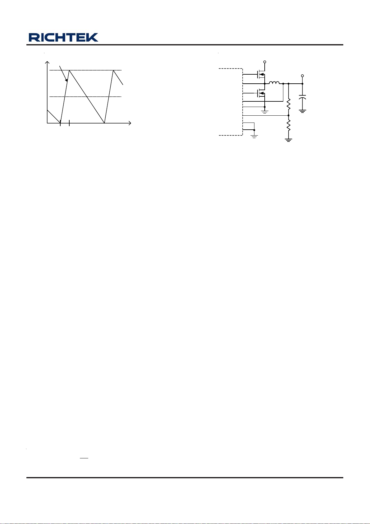
RT8208A/B
I
L
Slope = (VIN -V
0
t
ON
OUT
) / L
i
L, peak
i
Load
= i
t
L, peak
/ 2
UGATE
PHASE
LGATE
VOUT
GND
FB
G0
G1
V
IN
V
OUT
R1
R2
Figure 1. Boundary Condition of CCM/DEM
The switching waveforms may appear noisy and
Figure 2. Setting V
with a Resistor Divider
OUT
asynchronous when light loading causes diode-emulation
operation, but this is a normal operating condition that
results in high light-load efficiency. Trade-offs in DEM noise
vs. light-load efficiency is made by varying the inductor
value. Generally, low inductor values produce a broader
efficiency vs. load curve, while higher values result in higher
full-load efficiency (assuming that the coil resistance
remains fixed) and less output voltage ripple. The
disadvantages for using higher inductor values include
larger physical size and degraded load-transient response
(especially at low input voltage levels).
Output V oltage Transition Control
The RT8208A/B provides two digital control input G0 and
G1 to allow selection among four output voltages. The
output voltage is regulated by comparing the FB pin
(connected to VOUT via an external resistor divider) to
the internal 0.75V reference. The G0 and G1 digital input
control the gate of internal respective MOSFET whose
drain is connected to D0 and D1 respectively. Using Gx,
the user controls whether Dx is grounded or open, which
then controls the resistor divider ratio for V
OUT
. A logic
high signal on Gx will connect Dx to ground.
Forced-CCM Mode (EN = floating)
When the Gx input changes state, this change quickly
The low noise, forced-CCM mode (EN=floating) disables
causes three actions:
the zero-crossing comparator, which controls the low side
switch on-time. This causes the low side gate drive
waveform to become the complement of the high side
gate-drive waveform. This in turn causes the inductor
current to reverse at light loads as the PWM loop to
maintain a duty ratio VOUT/VIN. The benefit of forced-
CCM mode is to keep the switching frequency fairly
constant, but it comes at a cost: The no-load battery
current can be up to 10mA to 40mA, depending on the
external MOSFETs.
Output V oltage Setting (FB)
The output voltage can be adjusted from 0.75V to 3.3V by
setting the feedback resistor R1 and R2, see Figure 2.
With G0 and G1 in low state, the output voltage is at the
lowest value. Choose R2 to be approximately 20kΩ, and
1. D0 changes state.
2. The power good PGOOD output is temporarily latched
into its present state. This prevents chattering or false
tripping while V
moves to the new level.
OUT
3. When the Gx changes state whether DEM is set or
not, then enter the PWM mode and counts 32 clock
cycles. For the duration of 32 clock cycles, the OVP
and UVP function is masked. This behavior allows the
output to slew down to the new level without tripping
the OVP or UVP function when the Gx change causes
rapid change of Dx, which in turns cause a rapid change
at FB.
Output voltage is regulated through the FB pin via resistors
R1 through R4 as shown in Figure 3.
solve for R1 using the equation :
R1
⎛⎞
V = V 1+
OUT REF
where V
DS8208A/B-04 May 2011 www.richtek.com
×
⎜⎟
R2
⎝⎠
is 0.75V in typical.
REF
11

RT8208A/B
V
D0
D1
R3
R4
FB
GND
G1
G0
TON
Control
Logic
0.75V
Figure 3. Output Voltage Selection By G0 and G1 Input
OUT
R1
R2
G1
G0
Control
Logic
D0
D1
FB
GND
R4
R3
R1
R2
V
OUT
The following table shows the equations for VOUT as a
function of digital control input G0 and G1.
RT8208 A RT8208B
Output Voltage Equation
G0 G1 G0 G1
0 0 1 1
1 0 0 1
0 1 1 0
1 1 0 0
Note that the R
DS(ON)
V = x 0.75R2
OUT
V = x 0.75
OUT
V = x 0.75
OUT
V = x 0.75
OUT
of the internal MOSFET is in series
R1+R2
R1+(R2//R3)
(R2//R3)
R1+(R2//R4)
(R2//R4)
R1+(R2//R3//R4)
(R2//R3//R4)
with external resistor, which adds typically 10Ω in series.
Output Voltage Transition Operation
The digital input control pin Gx allows VOUT to transition
to both higher and lower values. For a down transition, the
rapid change Gx from high to low as sudden release either
of external resistors (R3 or R4) will cause FB to go above
the 0.75V threshold. At this time, the LGATE will drive
high to turn on the low side MOSFET and draw current
from the output capacitor via the inductor. LGATE will
remain on until FB falls to 0.75V, at which point a normal
UGATE switching cycle begins, see Figure4. For a down
transition, the low side MOSFET stays on before FB
reaches to 0.75V, thus the negative inductor current will
be increased. If the negative current is too large to trigger
NOCP, the low side MOSFET is turned off which can avoid
too much negative current to damage component. Refer
to the Negative Over Current Limit section for a full
description.
Gx
GND
FB
LGATE
UGATE
Initial
V
V
OUT
OUT
Final
V
OUT
Figure 4. Output Voltage Down Transition
Gx
GND
FB
UGATE
LGATE
V
OUT
Minimum
off-time
FB
Threshold
Final V
Initial V
OUT
OUT
Figure 5. Output Voltage Up Transition
12
DS8208A/B-04 May 2011www.richtek.com

RT8208A/B
)
μ
For an up transition (from lower to higher VOUT) as shown
in Figure5, the Gx change affects Dx and causes FB to
drop below the 0.75V trip point. This quickly trips the FB
comparator regardless of whether DEM is active or not,
generating an UGATE on-time and a subsequent LGATE
will be turned on. At the end of the minimum off-time
(400ns), if FB is still below 0.75V then another UGATE
on-time is started. This sequence continues until the FB
pin exceeds 0.75V.
Gx
GND
FB
UGATE
LGATE
V
OUT
Minimum
off-time
FB
Threshold
Final V
Initial V
OUT
OUT
Figure 6. Output Voltage Up Transition
with Overshooting
If the VOUT change is significant, there can be several
consecutive cycle of UGATE on-time followed by minimum
LGATE time. This can cause a rapid increase in inductor
current: typically it takes only a few switching cycles for
inductor current to rise up to the current limit. At some
point the FB voltage will rise up to the 0.75V reference
and the UGATE pulses will cease, but the inductor’ s LI
energy must then flow into the output capacitor. This can
create a significant overshoot as shown in Figure6.
The overshooting can be approximated by the following
equation, where ICL is the current limit, V
desired set point for the final voltage, L is in μH and C
FINAL
is the
OUT
is in μF.
2
⎛⎞
×
IL
CL
V = ( ) + V
MAX FIANL
⎜⎟
⎜⎟
C
OUT
⎝⎠
2
The Overshoot eliminator (Patent Pending) prevents output
voltage overshooting after rapid changes of Gx. This results
in a gradual change from V
OUT(INITIAL)
to V
prevents the buildup of high inductor current and reducing
overshoot.
Current Limit Setting (OCP)
RT8208A/B has cycle-by-cycle current limiting control.
The current limit circuit employs a unique “valley” current
sensing algorithm. If the magnitude of the current sense
signal at CS is above the current limit threshold, the PWM
is not allowed to initiate a new cycle (Figure 7).in order to
provide both good accuracy and a cost effective solution,
the RT8208A/B supports temperature compensated
MOSFET R
sensing. The CS pin should be
DS(ON)
connected to GND through the trip voltage setting resistor,
RCS. The CS terminal source 10μA ICS current, and the
trip level is set to the CS trip voltage, VCS as in the following
equation.
V(mV) = R(k) x 10A
CS CS
Ω
(
Inductor current is monitored by the voltage between the
PGND pin and the PHASE pin. So the PHASE pin should
be connected to the drain terminal of the low-side
MOSFET. ICS has temperature coefficient to compensate
the temperature dependency of the R
. PGND is used
DS(ON)
as the positive current sensing node. So PGND should
be connected to the source terminal of the bottom
MOSFET.
As the comparison is done during the OFF state, V
sets the valley level of the inductor current. Thus, the
load current at over current threshold, I
2
LOAD_OC
calculated as follows ;
CS Ripple
I = +
LOAD_OC
V
CS
= +
R2Lf V
DS(ON) IN
VI
R2
DS(ON)
−×
VV V
()
1
××
IN OUT OUT
×
In an over current condition, the current to the load exceeds
the current to the output capacitor thus the output voltage
tends to fall. Eventually, it crosses the under-voltage
protection threshold and shutdown.
OUT(FINAL)
, can be
and
CS
DS8208A/B-04 May 2011 www.richtek.com
13

RT8208A/B
I
L
I
L, peak
I
Load
I
LIM
0
t
Figure 7. “Valley” Current Limit
Negative Over Current Limit (CCM Mode Only)
The RT8208A/B also supports cycle-by-cycle negative over
current limiting in CCM Mode only. The over-current limit
is set to be negative but is the same absolute value as
the positive over current limit. If output voltage continues
to rising, the low side MOSEFT stays on, thus inductor
current is reduced and reverses direction after it reaches
zero. When there is too much negative current in the
inductor, the low side MOSFET is turned off and the current
flows to VIN through the body diode of the high side
MOSFET. Because this protection limits current to
discharge the output capacitor, output voltage tends to
rise, eventually hitting the over-voltage protection threshold
and shutdown. In order to prevent false OVP from triggering,
the low side MOSFET is turned on again 400ns after it is
turned off. If the device hits the negative over-current
threshold again before output voltage is discharged to the
target level, the low side MOSFET is turned off and process
repeats. It ensures maximum allowable discharge
capability when output voltage continues to rise. On the
other hand, if the output is discharged to the target level
before negative current threshold is reached, the low side
MOSFET is turned off, the high side MOSFET is then
turn on, and the device resumes normal operation.
MOSFET Gate Driver (UGATE, LGA TE)
The high-side driver is designed to drive high current, low
R
N-MOSFET(s). When configured as a floating
DS(ON)
driver, 5V bias voltage is delivered from VDDP supply. The
average drive current is proportional to the gate charge at
VGS = 5V times switching frequency. The instantaneous
drive current is supplied by the flying capacitor between
BOOT and PHASE pins. A dead time to prevent shoot
through is internally generated between high-side
MOSFET off to low side MOSFET on, and low-side
MOSFET off to high side MOSFET on. The low-side driver
is designed to drive high current, low R
N-MOSFETs.
DS(ON)
The internal pull-down transistor that drives LGATE low is
robust, with a 0.6Ω typical on resistance. A 5V bias voltage
is delivered from VDDP supply. The instantaneous drive
current is supplied by the flying capacitor between VDDP
and PGND.
For high current applications, some combinations of high
and low side MOSFETs might be encountered that will
cause excessive gate-drain coupling, which can lead to
efficiency-killing, EMI-producing shoot-through currents.
This is often remedied by adding a resistor in series with
BOOT, which increases the turn-on time of the high-side
MOSFET without degrading the turn-off time (Figure 8).
V
IN
BOOT
UGATE
PHASE
R
Figure 8. Reducing the UGATE Rise Time
Power Good Output (PGOOD)
The power good output is an open-drain output and requires
a pull-up resistor. When the output voltage is 25% above
or 10% below its set voltage, PGOOD will be pulled low. It
is held low until the output voltage returns to within these
tolerances once more. In soft-start, PGOOD is actively
held low and is allowed to transition high until soft-start is
over and the output reaches 93% of its set voltage. There
is a 2.5μs delay built into PGOOD circuitry to prevent
false transition.
When Gx changes state, PGOOD is immediately latched
into its present state for 32 clock cycle while VOUT and
FB are changed to the new level. After that the latch will
be disabled.
14
DS8208A/B-04 May 2011www.richtek.com

RT8208A/B
)
POR, UVLO and Soft-Start
Power On Reset (POR) occurs when VDD rises above to
approximately 4.3V. after POR is triggered. And then, the
RT8208A/B will reset the fault latch and prepare the PWM
for operation. Below 4.1V (MIN), the VDD under voltage
lockout (UVLO) circuitry inhibits switching by keeping
UGATE and LGATE low. A built-in soft-start is used to
prevent surge current from power supply input after EN is
enabled. The maximum allowed current limit is segmented
in 4 steps: 25%, 50%, 75% and 100% during this period,
each step is 128 UGATE clks. The current limit steps can
eliminate the V
folded-back in the soft-start duration.
OUT
Output Over Voltage Protection (OVP)
The output voltage can be continuously monitored for over
voltage protection. When the output voltage exceeds 25%
of the its set voltage threshold, over voltage protection is
triggered and the low side MOSFET is latched on. This
activates the low side MOSFET to discharge the output
capacitor. The RT8208A/B is latched once OVP is
triggered and can only be released by VDD or EN power
on reset. There is 20μs delay built into the over voltage
protection circuit to prevent false transitions.
When Gx changes state, the OVP function is masked for
32 clock cycle while VOUT and FB are changed to the
new level. After that the mask will be disabled.
Output Under Voltage Protection (UVP)
The output voltage can be continuously monitored for under
voltage protection. When the output voltage is less than
70% of its set voltage threshold, under voltage protection
is triggered and then both UGATE and LGATE gate drivers
are forced low. In order to remove the residual charge on
the output capacitor during the under voltage period, if
PHASE is greater than 1V, the LGATE is forced high until
PHASE is lower than 1V. There is 2.5μs delay built into
the under voltage protection circuit to prevent false
transitions. During soft-start, the UVP blanking time is
512 UGATE clks.
When Gx changes state, the UVP function is masked for
32 clock cycle while VOUT and FB change to the new
level, after which the mask is disable.
Output Inductor Selection
The switching frequency (on-time) and operating point (%
ripple or LIR) determine the inductor value as follows :
L =
×
LI
IR LOAD(MAX)
×−
TVV
(
ON IN OUT
Where LIR is the ratio of peak-to-peak ripple current to the
maximum average inductor current. Find a low-pass
inductor having the lowest possible DC resistance that
fits in the allowed dimensions. Ferrite cores are often the
best choice, although powdered iron is inexpensive and
can work well at 200kHz. The core must be large enough
and not to saturate at the peak inductor current (I
⎡⎤
L
⎛⎞
IR
I = I + I
PEAK LOAD(MAX) LOAD(MAX)
⎢⎥
⎣⎦
×
⎜⎟
2
⎝⎠
PEAK
) :
Output Capacitor Selection
The output filter capacitor must have low enough Equivalent
Series Resistance (ESR) to meet output ripple and load-
transient requirements, yet have high enough ESR to
satisfy stability requirements. The output capacitance
must also be high enough to absorb the inductor energy
while transiting from full-load to no-load conditions without
tripping the overvoltage fault latch.
Although Mach ResponseTM DRVTM dual ramp valley mode
provides many advantages such as ease-of-use, minimum
external component configuration, and extremely short
response time, due to not employing an error amplifier in
the loop, a sufficient feedback signal needs to be provided
by an external circuit to reduce the jitter level. The required
signal level is approximately 15mV at the comparing point.
This generates V
Ripple
= (V
/ 0.75) x 15mV at the output
OUT
node. The output capacitor ESR should meet this
requirement.
Output Capacitor Stability
Stability is determined by the value of the ESR zero relative
to the switching frequency. The point of instability is given
by the following equation :
f =
ESR
1
××
π
2 ESR C 4
OUT
f
SW
≤
Do not put high value ceramic capacitors directly across
the outputs without taking precautions to ensure stability.
DS8208A/B-04 May 2011 www.richtek.com
15

RT8208A/B
Large ceramic capacitors can have a high-ESR zero
frequency and cause erratic and unstable operation.
However, it is easy to add sufficient series resistance by
placing the capacitors a couple of inches downstream from
the inductor and connecting VOUT or FB divider close to
the inductor. There are two related but distinct ways
including double-pulsing and feedback loop instability to
identify the unstable operation. Double-pulsing occurs due
to noise on the output or because the ESR is too low that
there is not enough voltage ramp in the output voltage
signal. This “fools” the error comparator into triggering a
new cycle immediately after 400ns minimum off-time
period has expired. Double-pulsing is more annoying than
harmful, resulting in nothing worse than increased output
ripple. However, it may indicate the possible presence of
loop instability, which is caused by insufficient ESR. Loop
instability can result in oscillation at the output after line
or load perturbations that can trip the over voltage
protection latch or cause the output voltage to fall below
the tolerance limit. The easiest method for stability
checking is to apply a very zero-to-max load transient
and carefully observe the output-voltage-ripple envelope
for overshoot and ringing. It helps to simultaneously monitor
the inductor current with AC probe. Do not allow more
than one ringing cycle after the initial step-response under-
or over-shoot.
standard JEDEC 51-7 four layers thermal test board. The
maximum power dissipation at TA = 25°C can be calculated
by following formula :
P
= (125°C − 25°C)/(68°C/W) = 1.471W for
D(MAX)
WQFN-16L 3x3 package
The maximum power dissipation depends on operating
ambient temperature for fixed T
and thermal
J(MAX)
resistance θJA. For RT8208A/B package, the Figure 9 of
derating curve allows the designer to see the effect of
rising ambient temperature on the maximum power
allowed.
1.8
1.6
1.4
1.2
1.0
0.8
0.6
0.4
0.2
Maximum Power Dissipation (W) 1
0.0
0 25 50 75 100 125
Ambient Temperature (°C)
Four Layers PCB
Figure 9. Derating Curve for RT8208A/B Package
Thermal Considerations
For continuous operation, do not exceed absolute
maximum operation junction temperature. The maximum
power dissipation depends on the thermal resistance of
IC package, PCB layout, the rate of surroundings airflow
and temperature difference between junction to ambient.
The maximum power dissipation can be calculated by
following formula :
P
Where T
temperature, T
D(MAX)
= (T
− TA) / θ
J(MAX)
is the maximum operation junction
J(MAX)
is the ambient temperature and the θ
A
JA
JA
the junction to ambient thermal resistance.
For recommended operating conditions specification of
the RT8208A/B, the maximum junction temperature of
the die is 125°C. The junction to ambient thermal
resistance θJA is layout dependent. For WQFN-16L 3x3
packages, the thermal resistance θJA is 68°C/W on the
16
Layout Considerations
Layout is very important in high frequency switching
converter design. If designed improperly, the PCB could
radiate excessive noise and contribute to the converter
instability.
For best performance of the RT8208A/B, the following
guidelines should be strictly followed.
` Connect an RC low pass filter from VDDP to VDD, 1μF
and 10Ω are recommended. Place the filter capacitor
close to the IC.
` Keep current limit setting network as close as possible
is
to the IC. Routing of the network should be kept away
from to high voltage switching nodes to prevent it from
coupling.
` Connections from the drivers to the respective gate of
the high side or the low side MOSFET should be as
short as possible to reduce stray inductance.
DS8208A/B-04 May 2011www.richtek.com

` All sensitive analog traces and components such as
VOUT, FB, GND, EN/DEM, PGOOD, OC, VDD, and
TON should be placed away from high voltage switching
nodes such as PHASE, LGATE, UGATE, or BOOT
nodes to prevent it from coupling. Use internal layer(s)
as ground plane(s) and shield the feedback trace from
power traces and components.
` Current sense connections must always be made using
Kelvin connections to ensure an accurate signal, with
the current limit resistor located at the device.
` Power sections should connect directly to ground
plane(s) using multiple vias as required for current
handling (including the chip power ground connections).
Power components should be placed to minimize loops
and reduce losses.
RT8208A/B
DS8208A/B-04 May 2011 www.richtek.com
17
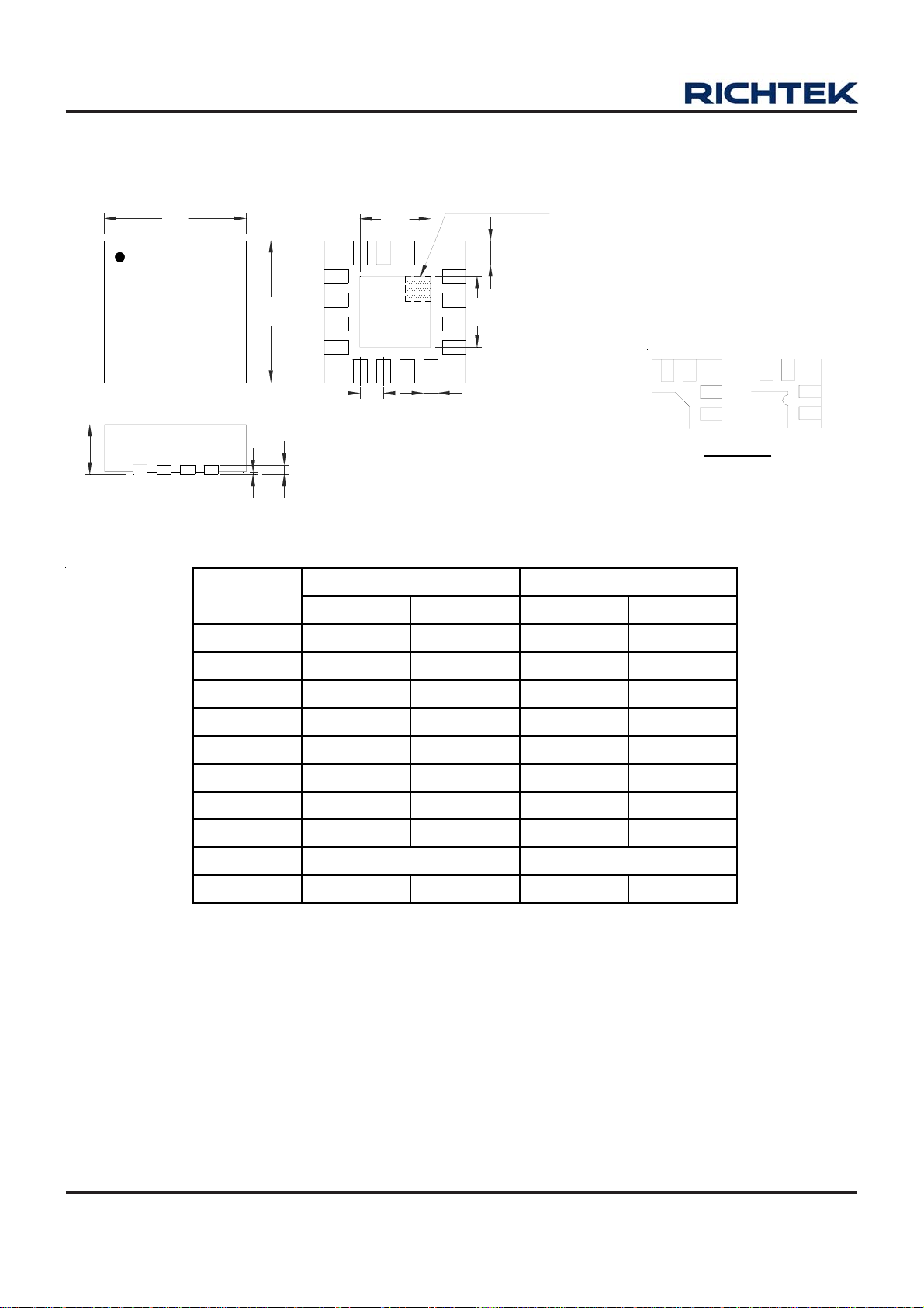
RT8208A/B
Outline Dimension
D
D2
L
SEE DETAIL A
1
E
e
A
A3
A1
E2
1
b
2
1
2
DETAIL A
Pin #1 ID and Tie Bar Mark Options
Note : The configuration of the Pin #1 identifier is optional,
but must be located within the zone indicated.
Dimensions In Millimeters Dimensions In Inches
Symbol
Min Max Min Max
A 0.700 0.800 0.028 0.031
A1 0.000 0.050 0.000 0.002
A3 0.175 0.250 0.007 0.010
b 0.180 0.300 0.007 0.012
D 2.950 3.050 0.116 0.120
D2 1.300 1.750 0.051 0.069
E 2.950 3.050 0.116 0.120
E2 1.300 1.750 0.051 0.069
e 0.500 0.020
L 0.350 0.450
Richtek Technology Corporation
Headquarter
5F, No. 20, Taiyuen Street, Chupei City
Hsinchu, Taiwan, R.O.C.
Tel: (8863)5526789 Fax: (8863)5526611
0.014 0.018
W-Type 16L QFN 3x3 Package
Richtek Technology Corporation
Taipei Office (Marketing)
5F, No. 95, Minchiuan Road, Hsintien City
Taipei County, Taiwan, R.O.C.
Tel: (8862)86672399 Fax: (8862)86672377
Email: marketing@richtek.com
Information that is provided by Richtek Technology Corporation is believed to be accurate and reliable. Richtek reserves the right to make any change in circuit
design, specification or other related things if necessary without notice at any time. No third party intellectual property infringement of the applications should be
guaranteed by users when integrating Richtek products into any application. No legal responsibility for any said applications is assumed by Richtek.
DS8208A/B-04 May 2011www.richtek.com
18

 Loading...