


RT8207
Complete DDRII/DDRIII Memory Power Supply Controller
General Description
The RT8207 provides a complete power supply for both
DDRII/DDRIII memory systems. It integrates a
synchronous PWM buck controller with a 3A sink/source
tracking linear regulator and a buffered low noise reference.
The PWM controller provides the high efficiency, excellent
transient response, and high DC output accuracy needed
for stepping down high-voltage batteries to generate low
voltage chipset RAM supplies in notebook computers.
The constant-on-time PWM control scheme handles wide
input/output voltage ratios with ease and provides 100ns
“instant-on” response to load transients while maintaining
a relatively constant switching frequency.
The RT8207 achieves high efficiency at a reduced cost
by eliminating the current-sense resistor found in
traditional current-mode PWMs. Efficiency is further
enhanced by its ability to drive very large synchronous
rectifier MOSFETs. The buck conversion allows this device
to directly step down high-voltage batteries for the highest
possible efficiency.
The 3A sink/source LDO maintains fast transient response
only requiring 20μF of ceramic output capacitance. In
addition, the LDO supply input is available externally to
significantly reduce the total power losses. The RT8207
supports all of the sleep state controls placing VTT at
High-Z in S3 and discharging VDDQ, VTT and VTTREF
(soft-off) in S4/S5.
Features
zz
PWM Controller
z
zz
``
` Resistor Progra mmable Current Limit by Low-Side
``
R
``
` Quick Load-Step Response within 100ns
``
``
` 1% V
``
``
` Fixed 1.8V (DDRII), 1.5V (DDRIII) or Adjustable
``
DS(ON)
OUT
Sense
Accuracy Over Line and Load
0.75V to 3.3V Output Range
``
` Battery Input Range 2.5V to 26V
``
``
` Resistor Programmable Frequency
``
``
` Over/Under Voltage Protection
``
``
` 4 Steps Current Limit During Soft-Start
``
``
` Drives Large Synchronous-Re ctifier FETs
``
``
` Power-Good Indicator
``
zz
z 3A LDO (VTT), Buffered Reference (VTTREF)
zz
``
` Capable to Sink and Source Up to 3A
``
``
` LDO Input Available to Optimize Power Losses
``
``
` Requires Only 20
``
``
` Buffered Low Noise 10mA VTTREF Output
``
``
` Accuracy
``
``
` Supports High-Z in S3 and Soft-Off in S4/S5
``
zz
z RoHS Compliant and Halogen Free
zz
±±
±20mV for Both VTTREF and VTT
±±
μμ
μF Ceramic Output Capacitor
μμ
Applications
z DDRII/DDRIII Memory Power Supplies
z Notebook Computers
z SSTL18, SSTL15 and HSTL Bus Termination
The RT8207 has all of the protection features including
thermal shutdown and is available in the WQFN-24L 4x4
Pin Configurations
(TOP VIEW)
package.
UGATE
BOOT
21 20 1924 2223
S3
FB
PHASE
25
S5
LGATE
18
17
16
15
14
13
TON
PGND
NC
CS
VDDP
VDD
PGOOD
VTT
Ordering Information
RT8207
Package Type
QW : WQFN-24L 4x4 (W-Type)
Lead Plating System
Note :
Richtek products are :
` RoHS compliant and compatible with the current require-
G : Green (Halogen Free and Pb Free)
VTTGND
VTTSNS
GND
MODE
VTTREF
DEM
VLDOIN
1
2
3
GND
4
5
6
78910 1211
NC
VDDQ
WQFN-24L 4x4
ments of IPC/JEDEC J-STD-020.
` Suitable for use in SnPb or Pb-free soldering processes.
DS8207-07 March 2011 www.richtek.com
1
RT8207
Marking Information
For marking information, contact our sales representative
directly or through a Richtek distributor located in your
area.
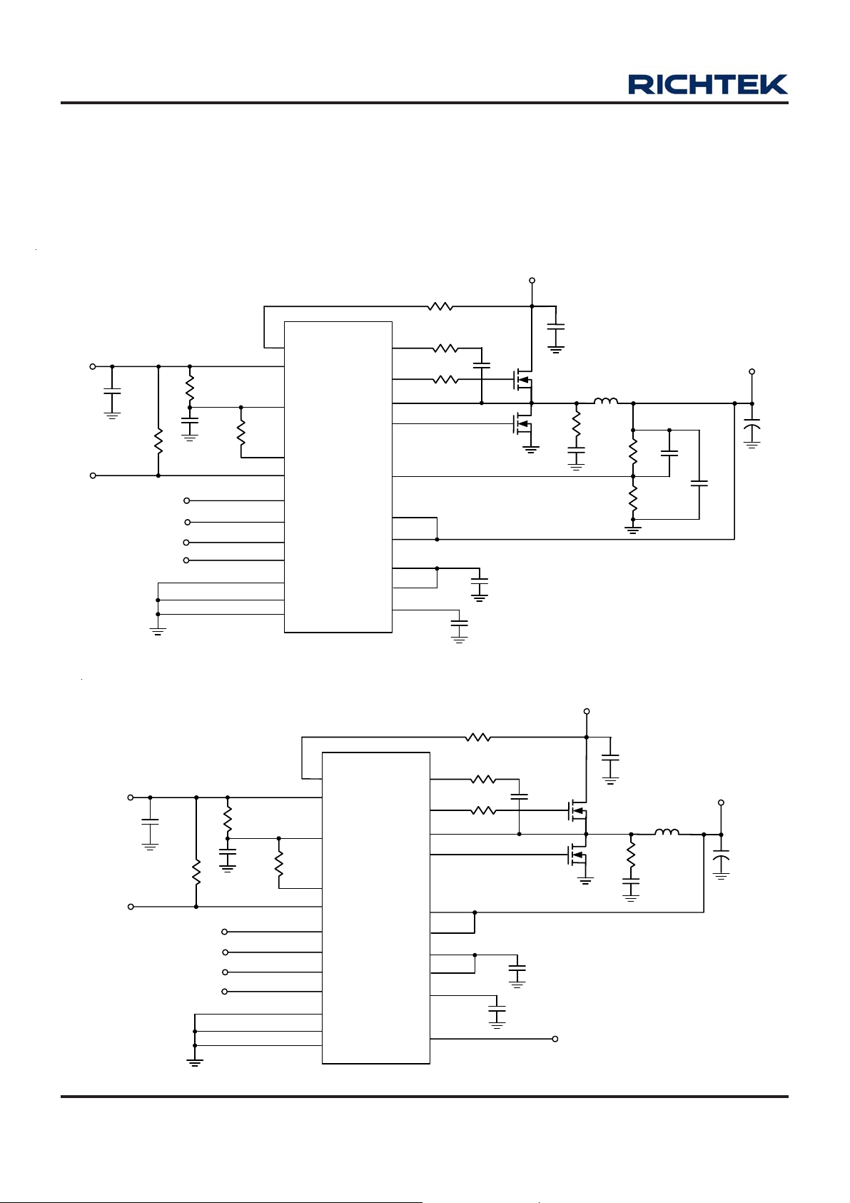
Typical Application Circuit
1
2
1
D
P
V
D
V
5
D
P
O
O
G
V
T
T
1
C
F
µ
1
2
R
k
0
0
1
V
T
/
T
R
E
C
F
o
n
V
D
C
D
Q
o
n
D
s
i
c
h
r
a
g
e
M
o
C
C
D
E
/
M
1
R
.
1
5
2
C
F
µ
1
o
l
r
t
o
l
r
t
d
e
M
3
E
p
x
o
,
s
e
d
5
1
4
3
R
.
6
5
k
1
6
1
3
1
0
1
1
4
6
P
a
d
(
2
5
)
1
8
1
R
T
O
N
V
D
D
P
D
D
V
S
C
D
O
O
G
P
S
3
S5
MODE
DEM
D
N
G
PGND
VTTGND
V
I
N
2
5
.
o
2
t
6
V
R
4
6
2
0
k
R
T
8
2
0
7
2
B
U
G
P
H
L
G
L
V
V
V
T
T
V
T
T
2
O
O
T
2
1
T
A
E
2
0
A
S
E
1
9
T
E
A
9
F
B
2
3
D
O
I
N
8
D
Q
D
2
4
T
T
V
2
N
S
S
5
R
E
F
5
0
6
R
B
C
4
0
1
.
µ
F
0
Q
S
C
2
0
2
3
N
0
3
5
C
8
1
0
µ
C
3
3
3
n
F
V
C
9
1
0
µ
F
x
3
V
V
D
D
Q
1
2
.
Q
1
B
C
0
S
9
L
1
1
µ
4
N
0
3
x
F
2
H
5
R
7
R
5
C
8
C
6
R
1
6
k
C
9
0
k
9
0
.
V
C
7
2
0
2
µ
F
1
µ
F
Figure A. Adjustable Voltage Regulator
V
I
N
2
5
V
.
2
V
o
t
6
R
4
6
2
0
k
C
R
T
8
R
2
0
2
1
T
O
N
5
P
D
D
V
V
5
O
D
O
G
P
V
T
T
1
C
F
µ
1
2
R
k
0
0
1
T
T
R
V
/
D
C
F
o
E
V
D
D
Q
C
o
s
i
c
e
h
g
a
r
M
C
C
D
/
M
R
1
5
.
1
2
C
F
µ
1
n
o
l
t
r
o
n
l
t
r
o
e
d
E
M
,
3
E
x
p
s
o
e
1
V
D
D
4
1
D
V
D
3
R
k
.
6
5
1
6
S
C
3
1
O
G
P
1
0
S
3
1
1
S5
4
MODE
6
DEM
a
d
d
P
2
)
5
(
8
1
1
D
N
G
PGND
VTTGND
7
2
B
P
G
U
H
P
L
G
D
O
V
V
L
T
T
V
T
T
V
2
O
O
T
2
1
A
T
E
2
0
A
S
E
1
9
A
T
E
8
D
D
Q
2
3
N
D
O
I
2
4
V
T
T
2
S
N
S
5
R
E
F
9
F
B
5
0
R
6
C
4
1
0
µ
.
F
0
2
B
S
3
Q
C
0
2
3
N
0
3
5
C
7
1
µ
0
x
F
2
C
3
3
n
F
D
V
D
P
N
G
f
D
8
1
0
µ
x
F
2
V
D
V
D
Q
1
8
V
.
5
V
.
1
Q
1
B
S
C
0
9
L
1
µ
H
4
3
N
0
D
o
f
r
D
o
r
D
1
5
R
7
C
5
I
D
R
I
I
I
I
R
/
C
6
2
2
0
µ
F
Figure B. Fixed Voltage Regulator
DS8207-07 March 2011www.richtek.com
2

Function Block Diagram
TRIG
GM
+
On-time
Compute
1-SHOT
+
-
VDDQ
TON
Comp
-
+
RT8207
R
PWM
QS
DRV
BOOT
UGATE
FB
VDD
S5
S3
MODE
115% V
70% V
Discharge
Mode
Select
V
REF
REF
REF
0.75V
+
-
-
+
SS Timer
90% V
PWM
OV
UV
Latch
S1 Q
Latch
S1 Q
REF
Thermal
Shutdown
Min. T
OFF
QTRIG
1-SHOT
DRV
Diode
-
+
+
-
+
-
Emulation
+
-
+
-
-
+
-
GM
+
VDD
10µA
PHASE
VDDP
LGATE
PGND
CS
DEM
PGOOD
VTTREF
VLDOIN
VTT
VTTSNS
GND
110% V
90% V
VTTREF
VTTREF
-
+
-
+
VTTGND
DS8207-07 March 2011 www.richtek.com
3
RT8207
Functional Pin Description
Pin No. Pin Name Pin Function
1 VTTGND Power Ground for the VTT_LDO.
2 VT T SNS
3,
25 (Exposed Pad)
4 MODE
5 VTTREF VTTREF Buffered Reference Output.
6 DE M
7, 17 NC No Internal Connection.
8 VD DQ
9 FB
10 S3 S3 Signal Input.
11 S5 S5 Signal Input
12 TON
13 PGOOD
14 VDD Supply Input for the Analog Supply.
15 VDDP Supply Input for the Low Gate Driver.
16 CS
18 PGND Power Ground for Low-Side MOSFET.
19 LGATE Low-Side Gate Driver Output for VDDQ.
20 PHASE
21 UGATE High-Side Gate Driver Output for VDDQ.
GND
Voltage Sense Input for the VTT_LDO. Connect to the terminal of the VTT_LDO
output capacitor
Analog Ground. The exposed pad must be soldered to a large PCB and
connected to GND for maximum power dissipation.
Output Discharge Mode Setting Pin. Connect to VDDQ for tracking discharge.
Connect to GND for non-tracking discharge. Connect to VDD for no discharge.
Diode-Emulation Mode Enable Pin. Connect to VDD will enable diode-emulation
mode. Connect to GND will always operate in forced CCM mode.
VDDQ Reference Input for VTT and VTTREF. Discharge current sinking terminal
for VDDQ non-tracking discharge. Output voltage feedback input for VDDQ
output if FB pin is connected to VDD or GND
VDDQ Output Setting Pin. Connect to GND for DDRIII (V
supply. The pin should be connect to VDD for DDRII (V
or be connected to a resistive voltage divider from VDDQ to GND to adjust the
output of PWM from 0.75V to 3.3V.
The pin is used to set the UGATE on time through a pull-up resistor connecting to
.
V
IN
Power-Good Open-Drain Output. This pin will be in HIGH state when VDDQ
output voltage is within the target range.
Current Limit Threshold Setting Input. Connect this pin to VDD through the
voltage setting resistor.
External Inductor Connection for VDDQ and it behaves as the current sense
comparator input for Low-Side MOSFET R
DS(ON)
DDQ
sensing.
= 1.5V) power
DDQ
= 1.8V) power supply
22 BOOT Boost Flying Capacitor Connection for VDDQ.
23 VLDOIN Power Supply for the VTT_LDO.
24 VTT Power Output for the VTT_LDO
DS8207-07 March 2011www.richtek.com
4
RT8207
Absolute Maximum Ratings (Note 1)
z Input Voltage, TON to GND ---------------------------------------------------------------------------------------------- –0.3V to 32V
z BOOT to GND -------------------------------------------------------------------------------------------------------------- –0.3V to 38V
z PHASE to GND
DC----------------------------------------------------------------------------------------------------------------------------- −0.3V to 32V
<20ns ------------------------------------------------------------------------------------------------------------------------ −8V to 38V
z PHASE to BOOT ---------------------------------------------------------------------------------------------------------- –6V to 0.3V
z VDD, VDDP, CS, MODE, S3, S5, VTTSNS, VDDQ, DEM to GND -------------------------------------------- –0.3V to 6V
z VTTREF, VTT, VLDOIN, FB, PGOOD to GND ---------------------------------------------------------------------- –0.3V to 6V
z UGATE to PHASE
DC----------------------------------------------------------------------------------------------------------------------------- −0.3V to 6V
<20ns ------------------------------------------------------------------------------------------------------------------------ −5V to 7.5V
z LGATE to GND
DC----------------------------------------------------------------------------------------------------------------------------- −0.3V to 6V
<20ns ------------------------------------------------------------------------------------------------------------------------ −2.5V to 7.5V
z PGND, VTTGND to GND ------------------------------------------------------------------------------------------------- –0.3V to 0.3V
z Power Dissipation, P
WQFN-24L 4x4 ----------------------------------------------------------------------------------------------------------- 1.923W
z Package Thermal Resistance (Note 2)
WQFN-24L 4x4, θJA------------------------------------------------------------------------------------------------------- 52°C/W
WQFN-24L 4x4, θJC------------------------------------------------------------------------------------------------------ 7°C/W
z Junction Temperature ----------------------------------------------------------------------------------------------------- 150°C
z Lead Temperature (Soldering, 10 sec.) ------------------------------------------------------------------------------- 260°C
z Storage Temperature Range -------------------------------------------------------------------------------------------- –65°C to 150°C
z ESD Susceptibility (Note 3)
HBM (Human Body Mode) ---------------------------------------------------------------------------------------------- 2kV
MM (Machine Mode) ------------------------------------------------------------------------------------------------------ 200V
@ TA = 25°C
D
Recommended Operating Conditions (Note 4)
z Input Voltage, V
z Control Voltage, V
z Junction Temperature Range-------------------------------------------------------------------------------------------- −40°C to 125°C
z Ambient Temperature Range-------------------------------------------------------------------------------------------- −40°C to 85°C
---------------------------------------------------------------------------------------------------------- 2.5V to 26V
IN
, VDD---------------------------------------------------------------------------------------------- 4.5V to 5.5V
DDP
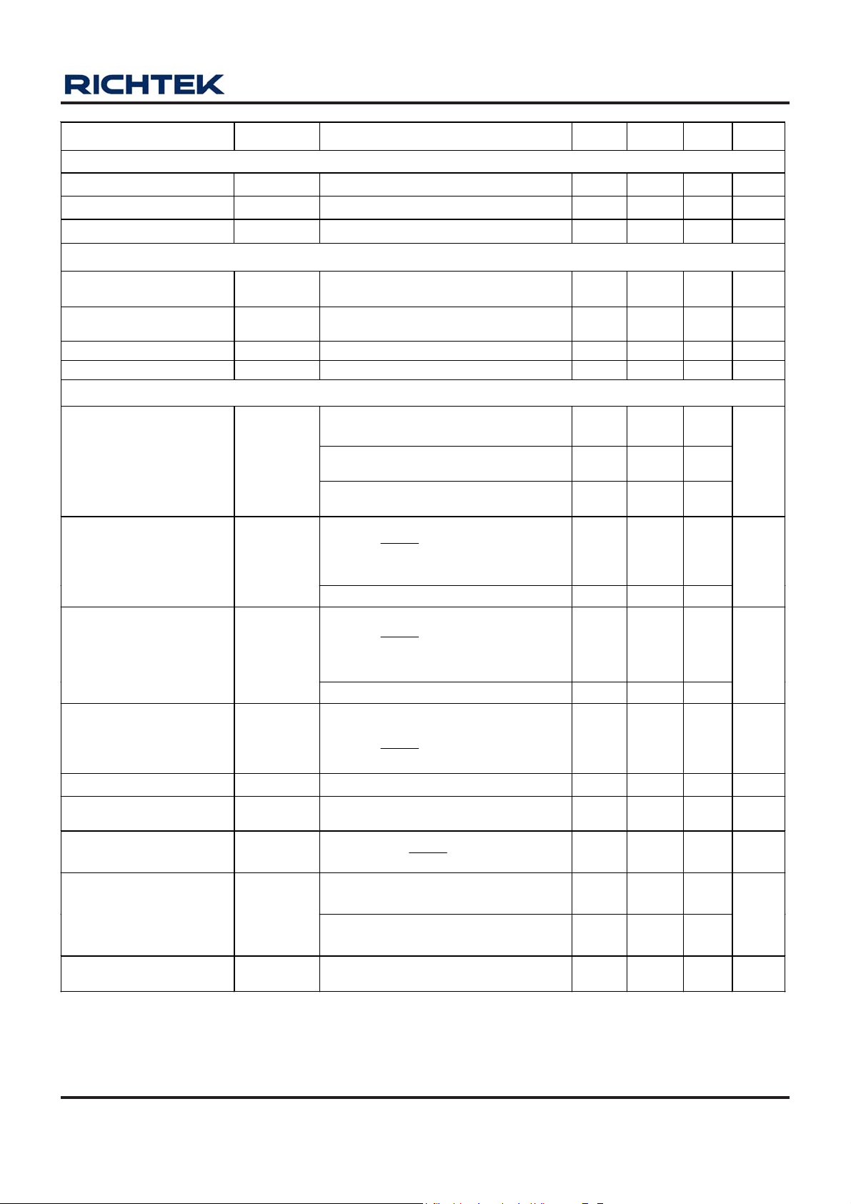
Electrical Characteristics
(V
= V
DD
= 5V, V
DDP
Parameter Symbol Test Conditions Min Typ Max Unit
PWM Controller
Quiescent Supply Current
(VDD + VDDP)
TON Operating Current R
I
I
DS8207-07 March 2011 www.richtek.com
BIAS Current VS5 = VS3 = 5V, VTT = No Load -- 1 -- μA
VLDOIN
Standby Current V
VLDOIN
= 15V, DEM = V
IN
, R
DD
= 1MΩ, T
TON
= 25°C, unless otherwise specified)
A
FB forced above the regulation point,
= 5V, V
V
S5
= 1MΩ -- 15 -- μA
TON
= 5V, VS3= 0, VTT = No Load -- 0.1 10 μA
S5
S3
= 0V
-- 470 1000 μA
To be continued
5
RT8207
Parameter Symbol Test Conditions Min Typ Max Unit
Shutdown current
= VS3 = 0V)
(V
S5
FB Reference Voltage V
Fixed VDDQ Output Voltage
V
TON -- 0.1 5
S3/S5/DEM = 0V −1 0.1 1
I
VDD = 4.5V to 5.5V 0.742 0.75 0.758 V
REF
FB = GND -- 1.5 --
FB = V
+ V
DD
VLDOIN
-- 0.1 10
DDP
μA
-- 0.1 1
-- 1.8 --
DD
V
FB Input Bias Current FB = 0.75V −1 0.1 1 μA
VDDQ Voltage Range 0.75 -- 3.3 V
On-Time, VIN = 15V R
= 1MΩ 267 334 401 ns
TON
Minimum Off-Time 250 400 550 ns
VDDQ Input Resistanc e -- 100 -- kΩ
VDDQ Shutdown Discharge
Resistance
V
= GND -- 15 -- Ω
S5
Curr ent Sensin g
CS Sink Current VCS > 4.5V, After UV Blank Time 9 10 11 μA
Current Comparator Offset GND − PHASE −15 -- 15 mV
Zero Crossing Threshold PHASE − GND, DEM = 5V −10 -- 5 mV
Fault Protection
Current Lim it (Pos itive)
GN D − PHASE, RCS = 5kΩ 35 50 65 mV
GN D − PHASE, R
= 20kΩ 170 200 230 mV
CS
Output UV Threshold 60 70 80 %
OVP Threshold
With respect to error comparator
threshold
10 15 20 %
OV Fault Delay FB forced above OV threshold -- 20 -- μs
VDDP Under voltage Lockout
Threshold
Rising edge, hysteresis = 20mV,
PWM disabled below this level
3.9 4.2 4.5 V
Current Limit Step Time at Soft Start Each step -- 128 -- clks
UV Blank Time From S5 signal going high -- 512 -- clks
Thermal Shutdown Hysteresis = 10°C -- 165 -- °C
Driver On-Resistance
UGATE Gate Driver (pull up) (BOOT − PHASE) forced to 5V -- 2 4 Ω
UGATE Gate Driver (sink) (BOOT − PHASE) forced to 5V -- 1 3 Ω
LGATE Gate Driver (pull up) LGATE, High State (source) -- 2.5 6 Ω
LGATE Gate Driver (pull down) LGATE, Low State (sink) -- 0.6 1.5 Ω
UGATE Gate Driver Source/Sink
Current
UGATE forced to 2.5V,
(BOOT − PHASE ) forced to 5V
-- 1 -- A
LGATE Gate Driver Source Current LGATE Forced to 2.5V -- 1 -- A
LGATE Gate Driver Sink Current LGATE Forced to 2.5V -- 3 -- A
Dead Time
LGATE Rising (PHASE = 1.5V) -- 40 --
UGATE Rising -- 40 --
Internal boost charging switch on
resistance
VDDP to BOOT, 10mA -- -- 80 Ω
To be continued
DS8207-07 March 2011www.richtek.com
6
ns
RT8207
Parameter Symbol Test Conditions Min Typ Max Unit
Logic I/O
Logic Input Low Voltage S3, S5, DEM Low -- -- 0.8 V
Logic Input High Voltage S3, S5, DEM High 2 -- -- V
Logic Input Current S3/S5/DEM = VDD/GND −1 0 1 μA
PGOOD (upper side t hreshold decid e by OV threshold)
Trip Threshold (falling)
Fault Propagation Delay
Output Low Voltage I
Leakage Current High state, forced to 5.0V -- -- 1 μA
VTT LDO TA = 25°C, Unless Otherwise specification
VTT Output Tolerance V
VTT Source Current Limit I
VTT Sink Current Limit I
VTT Leakage Current I
VTTFB Leakage Current I
VTT Discharge Current I
VTTREF Output Voltage V
VDDQ/2, VTTREF Output
Voltage Tolerance
VTTREF Source Current
Limit
VTTTOL
VTTOCLSRC
VTTOCLSNK
VTTLK
VTTSNSLK
DSCHRG
VTTREF
V
VTTREFTOL
I
VTTREFOCL
Measured at FB, with respect to
reference, no load. Hysteresis = 3%
Falling edge, FB forced below
PGOOD trip threshold
= 1mA -- -- 0.4 V
SINK
V
= V
DDQ
⏐I
⏐= 0A
VTT
V
= V
DDQ
⏐I
⏐ = 1A
VTT
= V
V
DDQ
⏐I
⏐= 2A,
VTT
VTT = 0.95
⎛⎞
⎜⎟
⎝⎠
LDOIN
LDOIN
LDOIN
V
DDQ
2
= 1.5V/1.8V,
= 1.5V/1.8V,
= 1.5V/1.8V,
×
,
−13 −10 −7 %
-- 2.5 -- μs
−20 -- +20
−30 -- +30
−40 -- +40
3 -- 6
PGOOD = High
VTT = 0V -- 2 --
VTT = 1.05
V
DDQ
⎛⎞
⎜⎟
⎝⎠
×
2
3 -- 6
PGOOD = High
VTT = VDDQ -- 2 -S5 = 5V, S3 = 0V,
VTT =
I
SINK
V
DDQ
S5 = S3 = 0V
V =
VTTREF
V
LDOIN
⏐I
VTTRE F
V
LDOIN
⏐I
VTTRE F
V
VTTRE F
V
⎛⎞
DDQ
⎜⎟
⎝⎠
2
= 1mA −1 -- 1 μA
= 0V, VTT = 0.5V,
V
⎛⎞
DDQ
⎜⎟
⎝⎠
= V
DDQ
-- 0.9/0.75 -- V
2
= 1.5V,
⏐ < 10mA
= V
DDQ
= 1.8V,
⏐ < 10mA
= 0V 10 40 80 mA
−10 -- 10 μA
10 30 -- mA
−15 -- +15
−18 -- +18
mV
A
A
mV
DS8207-07 March 2011 www.richtek.com
7

RT8207
Note 1. Stresses beyond those listed under “Absolute Maximum Ratings” may cause permanent damage to the device.
These are stress ratings only, and functional operation of the device at these or any other conditions beyond those
indicated in the operational sections of the specifications is not implied. Exposure to absolute maximum rating
conditions for extended periods may affect device reliability.
Note 2. θ
Note 3. Devices are ESD sensitive. Handling precaution is recommended.
Note 4. The device is not guaranteed to function outside its operating conditions.
is measured in the natural convection at TA = 25°C on a high effective 4 layers thermal conductivity test board of
JA
JEDEC 51-7 thermal measurement standard. The case point of θ
is on the expose pad for the WQFN package.
JC
DS8207-07 March 2011www.richtek.com
8

Typical Operating Characteristics
RT8207
VDDQ Efficiency v s . Output Current
100
DDRII
90
80
70
60
50
40
Efficiency (%)
30
20
10
0
0.001 0.01 0.1 1 10
DEM
PWM
VIN = 8V, V
S3 = GND, S5 = V
DDQ
Output Current (A)
VDDQ Efficiency vs. Output Current
100
DDRII
90
80
70
60
50
40
Efficiency (%)
30
20
10
0
0.001 0.01 0.1 1 10
DEM
Output Current (A)
PWM
VIN = 20V, V
S3 = GND, S5 = V
DDQ
= 1.8V,
DDP
= 1.8V,
DDP
VDDQ Efficiency vs. Output Current
100
DDRII
90
80
70
60
50
40
Efficiency (%)
30
20
10
0
0.001 0.01 0.1 1 10
DEM
PWM
VIN = 12V, V
S3 = GND, S5 = V
DDQ
Output Current (A)
VDDQ Efficiency vs. Output Current
100
DDRIII
90
80
70
60
50
40
Efficiency (%)
30
20
10
0
0.001 0.01 0.1 1 10
DEM
PWM
Output Current (A)
VIN = 8V, V
S3 = GND, S5 = V
DDQ
= 1.8V,
DDP
= 1.5V,
DDP
VDDQ Efficiency vs. Output Current
100
DDRIII
90
80
70
60
50
40
Efficiency (%)
30
20
10
0
0.001 0.01 0.1 1 10
DEM
PWM
Output Current (A)
VIN = 12V, V
S3 = GND, S5 = V
DDQ
Efficiency (%)
= 1.5V,
DDP
VDDQ Efficiency vs. Output Current
100
DDRIII
90
80
70
60
50
40
30
20
10
0
0.001 0.01 0.1 1 10
DEM
Output Current (A)
PWM
VIN = 20V, V
S3 = GND, S5 = V
DDQ
= 1.5V,
DDP
DS8207-07 March 2011 www.richtek.com
9

RT8207
Switching Frequency vs. Output Current
450
DDRII, VIN = 8V, V
400
350
300
250
200
150
100
Switching Frequency (kHz)
50
0
0.001 0.01 0.1 1 10
= 1.8V, S3 = GND, S5 = V
DDQ
PWM
DEM
Output Current (A)
Switching Frequency vs. Output Current
450
VIN = 20V, V
DDRII
400
350
300
250
200
150
100
Switching Frequency (kHz)
50
0
0.001 0.01 0.1 1 10
= 1.8V, S3 = GND, S5 = V
DDQ
PWM
DEM
Output Current (A)
DDP
DDP
Switching Frequency v s . Output Current
450
DDRII, VIN = 12V, V
400
350
300
250
200
150
100
Switching Frequency (kHz)
50
0
0.001 0.01 0.1 1 10
PWM
= 1.8V, S3 = GND, S5 = V
DDQ
DEM
Output Current (A)
Switching Frequency vs. Output Current
450
DDRIII, VIN = 8V, V
400
350
300
250
200
150
100
Switching Frequency (kHz)
50
0
0.001 0.01 0.1 1 10
PWM
= 1.5V, S3 = GND, S5 = V
DDQ
DEM
Output Current (A)
DDP
DDP
10
Switching Frequency vs. Output Current
450
VIN = 12V, V
DDRIII
400
350
300
250
200
150
100
Switching Frequency (kHz)
50
0
0.001 0.01 0.1 1 10
= 1.5V, S3 = GND, S5 = V
DDQ
PWM
DEM
Output Current (A)
DDP
Switching Frequency vs. Output Current
450
VIN = 20V, V
DDRIII
400
350
300
250
200
150
100
Switching Frequency (kHz)
50
0
0.001 0.01 0.1 1 10
= 1.5V, S3 = GND, S5 = V
DDQ
PWM
DEM
Output Current (A)
DS8207-07 March 2011www.richtek.com
DDP

RT8207
Output Voltage(V)
VDDQ O utp ut Vo l tage vs. Output Current
1.845
1.840
1.835
1.830
1.825
Output Voltage (V)
1.820
1.815
DDRII, VIN = 12V, V
DEM
PWM
0.001 0.01 0.1 1 10
= 1.8V, S3 = GND, S5 = V
DDQ
Output Current (A)
VTT Output Voltage vs. Output Current
0.9130
0.9125
0.9120
0.9115
0.9110
0.9105
0.9100
0.9095
DDRII, VIN = 12V, V
= 1.8V, S3 = S5 = V
DDQ
DDP
DDP
VDDQ Output Voltage vs. Output Current
Output Voltage (V)
1.540
1.535
1.530
1.525
1.520
1.515
DDRIII, VIN = 12V, V
DEM
PWM
0.001 0.01 0.1 1 10
= 1.5V, S3 = GND, S5 = V
DDQ
Output Current (A)
VTT Output Voltage vs. Output Current
0.7635
0.7630
0.7625
0.7620
0.7615
0.7610
Output Voltage (V)
0.7605
DDRIII, VIN = 12V, V
= 1.5V, S3 = S5 = V
DDQ
DDP
DDP
0.9090
-2 -1.6 -1.2 -0.8 -0.4 0 0.4 0.8 1.2 1.6 2
Output Current (A)
VTTREF Output Voltage vs. Output Current
Output Voltage (V)
0.918
0.916
0.914
0.912
0.910
0.908
0.906
0.904
0.902
DDRII, VIN = 12V, V
-10-8-6-4-2 0 2 4 6 810
= 1.8V, S3 = S5 = V
DDQ
Output Current (mA)
DDP
0.7600
-2 -1.6 -1.2 -0.8 -0.4 0 0.4 0.8 1.2 1.6 2
Output Current (A)
VTTREF Output Voltage vs. Output Current
Output Voltage (V)
0.768
0.766
0.764
0.762
0.760
0.758
0.756
0.754
DDRIII, VIN = 12V, V
-10-8-6-4-20246810
= 1.5V, S3 = S5 = V
DDQ
Output Current (mA)
DDP
DS8207-07 March 2011 www.richtek.com
11

RT8207
Standby Current vs. Input Voltage
390
No Load, DEM = 5V, S3 = S5 = 5V
380
370
360
350
Standby Current (uA)
340
330
7 9 11 13 15 17 19 21 23 25
Input Voltage (V)
VDDQ Voltage vs. Temperature
1.800
1.796
1.792
Shutdown Current vs. Input Voltage
3.0
No Load, DEM = 5V, S3 = S5 = GND
2.5
2.0
1.5
1.0
Shutdown Current (uA)
0.5
0.0
7 9 11 13 15 17 19 21 23 25
Input Voltage (V)
VDDQ Voltage vs. Temperature
1.538
1.534
1.530
1.526
1.788
VDDQ Voltage (V)
1.784
1.780
V
DDQ
(2V/Div)
V
TT
(1V/Div)
S5
(5V/Div)
PGOOD
(5V/Div)
DDRII, VIN = 12V, V
-40 -25 -10 5 20 35 50 65 80 95 110 125
= 1.8V, S3 = GDN, S5 = V
DDQ
Temperature
(°C)
DDP
VDDQ and VTT Start Up
VIN = 12V, V
No Load
= 1.8V, DEM = 5V, S3 = S5 = 5V
DDQ
Time (400μs/Div)
1.522
1.518
VDDQ Voltage (V)
1.514
1.510
V
DDQ
(1V/Div)
Inductor
Current
(10A/Div)
UGATE
(20V/Div)
LGATE
(5V/Div)
DDRIII, VIN = 12V, V
-40 -25 -10 5 20 35 50 65 80 95 110 125
= 1.5V, S3 = GDN, S5 = V
DDQ
Temperature
(°C)
DDP
VDDQ Start Up
VIN = 12V, V
DEM = 5V, S3 = GND
S5 = 5V, I
LOAD
DDQ
= 10A
= 1.8V
Time (1ms/Div)
12
DS8207-07 March 2011www.richtek.com

RT8207
V
DDQ
(2V/Div)
V
TT
(1V/Div)
V
TTREF
(1V/Div)
S5
(10V/Div)
V
DDQ_ac
(50mV/Div)
Shutdown
VIN = 12V, DEM = 5V, S3 = S5 = 5V, MODE = V
Time (200μs/Div)
No Load, Tracking Mode
VDDQ Load Transient Response
DDRII, VIN = 12V, V
I
= 1A to 10A, S3 = GND, S5 = 5V
LOAD
= 1.8V, DEM = 5V,
DDQ
DDQ
V
DDQ
(2V/Div)
V
TT
(1V/Div)
V
TTREF
(1V/Div)
S5
(10V/Div)
V
DDQ_ac
(50mV/Div)
Shutdown
VIN = 12V, DEM = 5V, S3 = S5 = 5V, MODE = GND
Time (2ms/Div)
Non-Tracking Mode
No Load
VDDQ Load Transient Response
DDRIII, VIN = 12V, V
I
= 1A to 10A, S3 = GND, S5 = 5V
LOAD
= 1.5V, DEM = 5V,
DDQ
Inductor
Current
(10A/Div)
UGATE
(20V/Div)
LGATE
(10V/Div)
V
TT_ac
(50mV/Div)
V
TTREF_ac
(20mV/Div)
I
LOAD
(2A/Div)
Time (20μs/Div)
VTT Load Transient Response
DDRII, VIN = 12V, V
I
= −2A to 2A, S3 = S5 = 5V
LOAD
= 1.8V, DEM = 5V,
DDQ
Inductor
Current
(10A/Div)
UGATE
(20V/Div)
LGATE
(10V/Div)
V
TT_ac
(20mV/Div)
V
TTREF_ac
(20mV/Div)
I
LOAD
(2A/Div)
Time (20μs/Div)
VTT Load Transient Response
DDRIII, VIN = 12V, V
I
= −2A to 2A, S3 = S5 = 5V
LOAD
= 1.5V, DEM = 5V,
DDQ
Time (500μs/Div)
Time (500μs/Div)
DS8207-07 March 2011 www.richtek.com
13

RT8207
V
DDQ
(1V/Div)
UGATE
(10V/Div)
LGATE
(5V/Div)
OVP
VIN = 12V, DEM = 5V, S3 = GND, S5 = 5V
No Load
Time (40μs/Div)
V
DDQ
(2V/Div)
Inductor
Current
(10A/Div)
UGATE
(20V/Div)
LGATE
(5V/Div)
UVP
VIN = 12V, DEM = 5V, S3 = GND, S5 = 5V
No Load
Time (20μs/Div)
14
DS8207-07 March 2011www.richtek.com

Application Information
)
RT8207
The RT8207 PWM controller provides the high efficiency,
excellent transient response, and high DC output accuracy
needed for stepping down high-voltage batteries to
generate low-voltage chipset RAM supplies in notebook
computers. Richtek's Mach ResponseTM technology is
specifically designed for providing 100ns “instant-on”
response to load steps while maintaining a relatively
required for the voltage on this capacitor to charge from
zero volts to VDDQ, thereby making the on-time of the
high-side switch directly proportional to output voltage and
inversely proportional to input voltage. The implementation
results in a nearly constant switching frequency without
the need of a clock generator.
TON = 3.85p x R
TON
x V
DDQ
/ (V
− 0.5)
IN
constant operating frequency and inductor operating point
over a wide range of input voltages. The topology
circumvents the poor load-transient timing problems of
fixed-frequency current-mode PWMs while avoiding the
problems caused by widely varying switching frequencies
And then the switching frequency is :
f = V
R
/ (V
DDQ
is a resistor connected from the input supply (VIN)
TON
x TON)
IN
to the TON pin.
in conventional constant-on-time and constant- off-time
PWM schemes. The DRVTM mode PWM modulator is
specifically designed to have better noise immunity for
such a single output application.
The 3A sink/source LDO maintains fast transient response
only requiring 20μF of ceramic output capacitance. In
addition, the LDO supply input is available externally to
significantly reduce the total power losses. The RT8207
Mode Selection (DEM) Operation
The DEM pin enables the supply. When the DEM pin is
connected to VDD, the controller will be enabled and
operated in diode-emulation mode. When the DEM pin is
connected to GND, the RT8207 will operate in forced-CCM
mode.
Diode-Emulation Mode (DEM = V DDP)
supports all of the sleep state controls placing VTT at
high-Z in S3 and discharging VDDQ, VTT and VTTREF
(soft-off) in S4/S5.
In diode-emulation mode, the RT8207 automatically
reduces switching frequency at light-load conditions to
maintain high efficiency. This reduction of the frequency
PWM Operation
The Mach Response
TM
DRVTM mode controller relies on
,
the output filter capacitor's effective series resistance
(ESR) to act as a current-sense resistor, so the output
ripple voltage provides the PWM ramp signal. Refer to the
function diagrams of the RT8207, the synchronous high-
side MOSFET will be tuned on at the beginning of each
cycle. After the internal one-shot timer expires, the
MOSFET will be turned off. The pulse width of this one
shot is determined by the converter's input and output
voltages to keep the frequency fairly constant over the
input voltage range. Another one-shot sets a minimum
off-time (400ns typ.).
is achieved smoothly and without increasing VDDQ ripple
or load regulation. As the output current decreases from
heavy-load condition, the inductor current will also be
reduced, and eventually comes to the point that its valley
touches zero current, which is the boundary between
continuous conduction and discontinuous conduction
modes. By emulating the behavior of diodes, the low-side
MOSFET allows only partial of negative current when the
inductor freewheeling current reaches negative. As the load
current is further decreased, it takes longer time to
discharge the output capacitor to the level than requires
the next “ON” cycle. The on-time is kept the same as
that in the heavy-load condition. In reverse, when the
output current increases from light load to heavy load, the
On-Time Control (TON)
The on-time one-shot comparator has two inputs. One
input looks at the output voltage, while the other input
samples the input voltage and converts it into a current.
This input voltage-proportional current is used to charge
an internal on-time capacitor. The on-time is the time
DS8207-07 March 2011 www.richtek.com
switching frequency increases to the preset value as the
inductor current reaches the continuous conducting
condition. The transition load point to the light-load
operation can be calculated as follows (Figure 1) :
−
VV
(
IN DDQ
IT
LOAD(SKIP) ON
where T
≈×
is On-time.
ON
2L
15

RT8207
I
L
Slope = (VIN - V
DDQ
) / L
i
L, peak
i
Load
= i
L, peak
/ 2
I
L
I
L, peak
I
Load
I
LIM
0
t
ON
t
Figure 1. Boundary condition of CCM/DCM
The switching waveforms may appear noisy and
asynchronous when light loading causes diode-emulation
operation, but this is a normal operating condition that
results in high light-load efficiency. Trade-offs in DEM noise
vs. light-load efficiency are made by varying the inductor
value. Generally, low inductor values produce a broader
efficiency vs. load curve, while higher values result in higher
full-load efficiency (assuming that the coil resistance
remains fixed) and less output voltage ripple. The
disadvantages for using higher inductor values include
larger physical size and degrades load-transient response
(especially at low input-voltage levels).
Forced-CCM Mode (DEM = GND)
The low-noise, Forced-CCM mode (DEM = GND) disables
the zero-crossing comparator, which controls the low-side
switch on-time. This causes the low-side gate-drive
waveform to become the complement of the high-side gate-
drive waveform. This in turn causes the inductor current
to reverse at light loads as the PWM loop maintains a
duty ratio of V
DDQ/VIN
. The benefit of Forced-CCM mode
is to keep the switching frequency fairly constant, but it
comes at a cost : The no-load battery current can be up
to 10mA to 40mA, depending on the external MOSFETs.
Current-Limit Setting for V DDQ (CS)
The RT8207 provides cycle-by-cycle current limiting
control. The current-limit circuit employs a unique “valley”
current sensing algorithm. If the magnitude of the current-
sense signal at the PHASE pin is above the current-limit
threshold, the PWM is not allowed to initiate a new cycle
(Figure 2). The actual peak current is greater than the
current-limit threshold by an amount equal to the inductor
ripple current. Therefore, the exact current-limit
characteristic and maximum load capability are a function
of the sense resistance, inductor value, and battery and
output voltage.
16
0
t
Figure 2. “valley” Current -Limit
The RT8207 uses the on-resistance of the synchronous
rectifier as the current-sense element. Use the worse-
case maximum value for R
from the MOSFET
DS(ON)
datasheet, and add a margin of 0.5%/°C for the rise in
R
The R
the current limit threshold. The resistor R
with temperature.
DS(ON)
setting resistor between CS pin and VDD sets
ILIM
is connected
ILIM
to a 10μA current source from the CS pin. When the voltage
drop across the low-side MOSFET equals the voltage
across the R
setting resistor, positive current limit will
ILIM
be activated. The high-side MOSFET will not be turned
on until the voltage drop across the MOSFET falls below
the current limit threshold.
Choose a current limit setting resistor by following
equation :
R
= I
ILIM
x R
LIM
DS(ON)
/ 10μA
Carefully observe the PC board layout guidelines to ensure
that noise and DC errors do not corrupt the current-sense
signal seen by the PHASE pin and PGND.
Current Protection for VTT
The LDO has an internally fixed constant over-current
limiting of 4.5A while operating at normal condition. This
over-current point is reduced to 2A before the output
voltage comes within 5% of its set voltage or goes outside
of 10% of its set voltage.
MOSFET Gate Driver (UGATE, LGA TE)
The high-side driver is designed to drive high-current, low
R
N-MOSFET(s). When configured as a floating driver,
DS(ON)
the 5V bias voltage will be delivered from the VDDP supply.
The average drive current is proportional to the gate charge
at VGS = 5V times switching frequency. The instantaneous
drive current is supplied by the flying capacitor between
BOOT and PHASE pins.
DS8207-07 March 2011www.richtek.com

RT8207
A dead time to prevent shoot through is internally
generated between high-side MOSFET off to low-side
MOSFET on, and low-side MOSFET off to high-side
MOSFET on.
The low-side driver is designed to drive high current, low
R
N-MOSFET(s). The internal pull-down transistor
DS(ON)
that drives LGATE low is robust, with a 0.4Ω typical on-
resistance. A 5V bias voltage is delivered from VDDP
supply. The instantaneous drive current is supplied by the
flying capacitor between VDDP and PGND.
For high-current applications, some combinations of high-
and low-side MOSFETs might be encountered that will
cause excessive gate-drain coupling, which can lead to
efficiency-killing, EMI-producing shoot-through currents.
This is often remedied by adding a resistor in series with
the BOOT pin, which increases the turn-on time of the
high-side MOSFET without degrading the turn-off time
(Figure 3).
V
IN
BOOT
UGATE
PHASE
+5V
10
Figure 3. Reducing the UGATE Rise Time
Power-Good Output (PGOOD)
The power good output is an open-drain output and requires
a pull-up resistor. When the output voltage is 15% above
or 10% below its set voltage, PGOOD will be pulled low.
It is held low until the output voltage returns to within
these tolerances once more. In soft start, the PGOOD
pin will be actively held low and is allowed to transition
high until soft start is over and the output reaches 93% of
its set voltage. There is a 2.5μs delay built into PGOOD
circuitry to prevent the false transition.
UVLO Protection
The RT8207 has a VDDP supply under-voltage lockout
protection (UVLO). When the VDDP voltage is lower than
4.3V (typ.), VDDQ, VTT and VTTREF will be shut off. This
is a non-latch protection.
Soft-Start
A build-in soft-start of VDDQ is used to prevent surge
current from power supply input after S5 is enabled. The
maximum allowed current limit is segmented in 4 steps:
25%, 50%, 75% and 100% and each step duration is 128
cycles. The current limit steps can minimize the VDDQ
folded-back in the soft-start duration when the fixed or
adjustable output is determined by the RT8207.
The soft-start function of the VTT is achieved by the current
clamp. The current limit threshold is also changed in two
stages using an internal power-good signal dedicated for
LDO. During VTT is below the power-good threshold, the
current limit level is 2A. This allows the output capacitors
to be charged with low and constant current that gives
linear ramp up of the output. When the output comes up
to the good state, the over-current limit is released to
4.5A.
Output Over voltage Protection (OVP)
The output voltage can be continuously monitored for over
voltage protection. When over voltage protection is
enabled, if the output exceeds 15% of its set voltage
threshold, over voltage protection will be triggered and the
LGATE low-side gate drivers will be forced high. This
activates the low-side MOSFET switch, which rapidly
discharges the output capacitor and reduces the input
voltage.
The RT8207 will be latched once the OVP is triggered
and can only be released by VDD power-on reset or S5.
There is a 20μs delay built into the over voltage protection
circuit to prevent false transitions.
Note that LGATE latching high causes the output voltage
to dip slightly negative when energy has been previously
stored in the LC tank circuit. For loads that cannot tolerate
a negative voltage, place a power Schottky diode across
the output to act as a reverse polarity clamp.
If the over voltage condition is caused by a short in high-
side switch, turning the low-side MOSFET on 100%
creates an electrical short between the battery and GND,
blowing the fuse and disconnecting the battery from the
output.
Output Under voltage Protection (UVP)
The output voltage can be continuously monitored for under
DS8207-07 March 2011 www.richtek.com
17

RT8207
V
voltage protection. When the under voltage protection is
enabled, if the output is less than 70% of its set voltage
threshold, the under voltage protection is triggered, then
both UGATE and LGATE gate drivers are forced low while
entering soft-discharge mode. During soft-start, the UVP
will be blanked around 512 cycles.
Thermal Protection
The RT8207 monitors the temperature of itself. If the
temperature exceeds the threshold value, +165°C (typ.),
the PWM output, VTTREF and VTT will be shut off. The
RT8207 is latched once the thermal shutdown is triggered
and can only be released by VDD power-on reset or S5.
Output V oltage Setting (FB)
The RT8207 can be used for both of DDR2 (VDDQ = 1.8V)
and DDR3 (VDDQ = 1.5V) power supply and it adjustable
output voltage (0.75V < VDDQ < 3.3V) by connecting FB
pin as shown in Table 1.
Table 1. FB and Output Voltage Setting
FB VDDQ (V)
VDD 1.8 V
GND 1.5 V
FB
Resistors
Adjustable V
TT REF and
VTT
/2 DDR2
DDQ
/2 DDR3
DDQ
/2
DDQ
NOTE
0.75V < V
< 3.3V
DDQ
VTT Linear Regulator and VTTREF
RT8207 integrates high performance low-dropout linear
regulator that is capable of sourcing and sinking current
up to 3A (VDDQ>= 1.8V). This VTT linear regulator
employs ultimate fast response feedback loop so that
small ceramic capacitors are enough to keep tracking the
VTTREF within 40mV at all conditions including fast load
transient. To achieve tight regulation with minimum effect
of wiring resistance, a remote sensing terminal, VTTSNS,
should be connected to the positive node of the VTT output
capacitor(s) as a separate trace from the VTT pin. For
stable operation, total capacitance of the VTT output
terminal can be equal to or greater than 20μF. It is
recommended to attach two 10μF ceramic capacitors in
parallel to minimize the effect of ESR and ESL. If ESR of
the output capacitor is greater than 2mΩ, insert an RC
filter between the output and VTTSNS input to achieve
loop stability. The RC filter time constant should be almost
the same or slightly lower than the time constant made
by the output capacitor and its ESR. The VTTREF block
consists of on-chip 1/2 divider, LPF and buffer. This regulator
also has sink and source capability up to 10mA. Bypass
VTTREF to GND by a 33nF ceramic capacitor for stable
operation.
Outputs Management by S3 and S5 Control
Connect a resistor voltage-divider at the FB between
VDDQ and GND to adjust the respective output voltage
between 0.75V and 3.3V (Figure 4). Choose R2 to be
approximately 10kΩ and solve for R1 using the equation
as follows :
⎡⎤
R1
VV1
=×+
DDQ REF
where V
is 0.75V (typ.).
REF
⎛⎞
⎢⎥
⎜⎟
R2
⎝⎠
⎣⎦
V
IN
UGATE
PHASE
LGATE
VDDQ
FB
GND
R1
R2
V
DDQ
Figure 4. Setting VDDQ with a Resistor-Divider
In DDRII/DDRIII memory applications, it is important to
keep VDDQ always higher than VTT/VTTREF including
both start-up and shutdown. The RT8207 provides this
management by simply connecting both S3 and S5
terminals to the sleep-mode signals such as SLP_S3 and
SLP_S5 in notebook PC system. All of VDDQ, VTTREF
and VTT are turned on at S0 state (S3 = S5 = high). In S3
state (S3 = low, S5 = high), VDDQ and VTTREF voltages
are kept on while VTT is turned off and left at high
impedance (high-Z) state. The VTT output is floated and
does not sink or source current in this state. In S4/S5
states (S3 = S5 = low), all of the three outputs are
disabled. Outputs are discharged to ground according to
the discharge mode selected by the MODE pin (see VDDQ
and VTT Discharge Control section). Each state code
represents as follows; S0 = full ON, S3 = suspend to
RAM (STR), S4 = suspend to disk (STD), S5 = soft OFF.
(See Table 2)
DS8207-07 March 2011www.richtek.com
18

RT8207
Table 2. S3 and S5 Truth Table
STATE S3 S5 VDDQ
S0 Hi Hi On
S3 Lo Hi On
S4/S5 Lo Lo
Off
(Discharge)
STATE VTTREF VTT
S0 On On
S3 On Off (Hi-Z)
S4/S5
Off
(Discharge)
Off
(Discharge)
V DDQ a nd VTT Discharge Control (MODE)
The RT8207 discharge VDDQ, VTTREF and VTT outputs
during S3 and S5 are both low. There are two different
discharge modes. The discharge mode can be set by
connecting MODE pin as shown in Table 3.
Table 3. Discharge Selection
MODE Discharge Mode
VDD N o discharge
VDDQ Tracking discharge
GND Non-tracking discharge
When in tracking discharge mode, the RT8207 discharges
outputs through the internal VTT regulator transistors and
VTT output tracks half of VDDQ voltage during this
discharge. Note that VDDQ discharge current flows via
VLDOIN to VTTGND, thus VLDOIN must be connected to
VDDQ in this mode. The internal LDO can handle up to
3A and can be dischargeed quickly. After VDDQ is
discharged down to 0.15V, the terminal LDO will be turned
off and the operation mode will be changed to the non-
tracking discharge mode.
When in non-tracking discharge mode, the RT8207
discharges outputs using internal MOSFETs which are
connected to VDDQ and VTT. The current capability of
these MOSFETs are limited to discharge slowly. Note that
VDDQ discharge current flows from VDDQ to GND in this
mode. In case of no discharge mode, the RT8207 does
not discharge output charge at all.
Output Inductor Selection
The switching frequency (on-time) and operating point (%
ripple or LIR) determine the inductor value as follows :
×−
T(VV)
ON IN DDQ
=
L
×
LI
IR LOAD(MAX)
where LIR is the ratio of the peak to peak ripple current to
the average inductor current.
Find a low-loss inductor having the lowest possible DC
resistance that fits in the allotted dimensions. Ferrite cores
are often the best choice, although powdered iron is
inexpensive and can work well at 200kHz. The core must
be large enough to prevent it from saturating at the peak
inductor current (I
I
= I
PEAK
LOAD(MAX)
) :
PEAK
+ [(LIR / 2) x I
LOAD(MAX)
]
This inductor ripple current also impacts transient-response
performance, especially at low VIN−VDDQ differences.
Low inductor values allow the inductor current to slew
faster, replenishing charge removed from the output filter
capacitors by a sudden load step. The peak amplitude of
the output transient (V
transient. The V
SAG
) is also a function of the output
SAG
is also features a function of the
maximum duty factor, which can be calculated from the
on-time and minimum off-time :
V
SAG
(I ) L (T T )
=
××××−×+
2C V V T V T T
OUT DDQ IN ON DDQ ON OFF(MIN)
Δ××+
Where minimum off-time (T
2
LOAD ON OFF(MIN)
⎡⎤
⎣⎦
OFF(MIN)
)=400ns(typical).
()
Output Capacitor Selection
The output filter capacitor must have low enough ESR to
meet output ripple and load-transient requirements, yet
have high enough ESR to satisfy stability requirements.
Also, the capacitance value must be high enough to
absorb the inductor energy going from a full-load to no-
load condition without tripping the OVP circuit.
For CPU core voltage converters and other applications
where the output is subject to violent load transients, the
output capacitor's size depends on how much ESR is
needed to prevent the output from dipping too low under a
load transient. Ignoring the sag due to finite capacitance:
V
≤
I
LOAD(MAX)
P-P
ESR
In non-CPU applications, the output capacitor's size
depends on how much ESR is needed to maintain an
acceptable level of output voltage ripple :
V
ESR
≤
where V
LI
P-P
×
IR LOAD(MAX)
is the peak-to-peak output voltage ripple.
P-P
DS8207-07 March 2011 www.richtek.com
19

RT8207
Organic semiconductor capacitor(s) or specialty polymer
capacitor(s) are recommended.
For low input-to-output voltage differentials (VIN/VDDQ
< 2), additional output capacitance is required to maintain
stability and good efficiency in ultrasonic mode.
The amount of overshoot due to stored inductor energy
can be calculated as :
2
V
SOAR
where I
(I ) L
PEAK
=
××
2C V
is the peak inductor current.
PEAK
×
OUT DDQ
Output Capacitor Stability
Stability is determined by the value of the ESR zero relative
to the switching frequency. The point of instability is given
by the following equation :
=≤
f
ESR
×× ×
2 ESR C 4
1f
π
OUT
SW
Do not put high-value ceramic capacitors directly across
the outputs without taking precautions to ensure stability.
Large ceramic capacitors can have a high- ESR zero
frequency and cause erratic, unstable operation. However,
it is easy to add enough series resistance by placing the
capacitors a couple of inches downstream from the
inductor and connecting VDDQ or the FB divider close to
the inductor.
Unstable operation manifests itself in two related and
distinctly different ways: double-pulsing and feedback loop
instability.
Double-pulsing occurs due to noise on the output or
because the ESR is so low that there is not enough voltage
ramp in the output voltage signal. This “fools” the error
comparator into triggering a new cycle immediately after
the 400ns minimum off-time period has expired. Double-
pulsing is more annoying than harmful, resulting in nothing
worse than increased output ripple. However, it may
indicate the possible presence of loop instability, which
is caused by insufficient ESR.
The easiest method for checking stability is to apply a
very fast zero-to-max load transient and carefully observe
the output-voltage-ripple envelope for overshoot and ringing.
It helps to simultaneously monitor the inductor current
with an AC current probe. Do not allow more than one
cycle of ringing after the initial step-response under- or
over-shoot.
Thermal Considerations
For continuous operation, do not exceed absolute
maximum operation junction temperature. The maximum
power dissipation depends on the thermal resistance of
IC package, PCB layout, the rate of surroundings airflow
and temperature difference between junction to ambient.
The maximum power dissipation can be calculated by
following formula :
P
Where T
temperature, T
D(MAX)
= ( T
J(MAX)
- TA ) / θ
J(MAX)
JA
is the maximum operation junction
is the ambient temperature and the θ
A
JA
the junction to ambient thermal resistance.
For recommended operating conditions specification of
RT8207, the maximum junction temperature is 125°C. The
junction to ambient thermal resistance θJA is layout
dependent. For WQFN-24L 4x4 packages, the thermal
resistance θJA is 54°C/W on the standard JEDEC 51-7
four layers thermal test board. The maximum power
dissipation at T
= 25°C can be calculated by following
A
formula :
P
= (125°C − 25°C) / (52°C/W) = 1.923W for
D(MAX)
WQFN-24L 4x4 packages
The maximum power dissipation depends on operating
ambient temperature for fixed T
and thermal
J(MAX)
resistance θJA. For RT8207 packages, the Figure 5 of
derating curves allows the designer to see the effect of
rising ambient temperature on the maximum power
allowed.
is
Loop instability can result in oscillations at the output
after line or load perturbations that can trip the over-voltage
protection latch or cause the output voltage to fall below
the tolerance limit.
20
DS8207-07 March 2011www.richtek.com

RT8207
2.0
1.8
1.6
1.4
1.2
1.0
0.8
0.6
0.4
0.2
Maximum Power Dissipation (W)
0.0
0 25 50 75 100 125
WQFN-24L 4x4
Four Layers PCB
Ambient Temperature (°C)
Figure 5. Derating Curves for RT8207 Packages
Layout Considerations
Layout is very important in high frequency switching
converter design. If the IC is designed improperly, the PCB
could radiate excessive noise and contribute to the
converter instability. Certain points must be considered
before starting a layout for the RT8207.
` The output capacitor for VTT should be placed close to
the pin with short and wide connection in order to avoid
additional ESR and/or ESL of the trace.
` VTTSNS should be connected to the positive node of
VTT output capacitor(s) as a separate trace from the high
current power line and is strongly recommended to avoid
additional ESR and/or ESL. If it is needed to sense the
voltage of the point of the load, it is recommended to
attach the output capacitor(s) at that point. Also, it is
recommended to minimize any additional ESR and/or
ESL of ground trace between GND pin and the output
capacitor(s).
` Current sense connections must always be made using
Kelvin connections to ensure an accurate signal, with
the current limit resistor located at the device.
` Power sections should connect directly to ground
plane(s) using multiple vias as required for current handling
(including the chip power ground connections). Power
components should be placed to minimize loops and
reduce losses.
` Connect an RC low-pass filter from VDDP to VDD, 1μF
and 5.1Ω are recommended. Place the filter capacitor
close to the IC.
` Keep current limit setting network as close as possible
to the IC. Routing of the network should avoid coupling
to high-voltage switching node.
` Connections from the drivers to the respective gate of
the high-side or the low-side MOSFET should be as short
as possible to reduce stray inductance.
` All sensitive analog traces and components such as
VDDQ, FB, PGND, DEM, PGOOD, CS, VDD, and TON
should be placed away from high-voltage switching nodes
such as PHASE, LGATE, UGATE, or BOOT nodes to
avoid coupling. Use internal layer(s) as ground plane(s)
and shield the feedback trace from power traces and
components.
` VLDOIN should be connected to VDDQ output with short
and wide trace. If different power source is used for
VLDOIN, an input bypass capacitor should be placed to
the pin as close as possible with short and wide trace.
DS8207-07 March 2011 www.richtek.com
21

RT8207
Outline Dimension
D
E
A
A3
A1
D2
SEE DETAIL A
L
1
E2
1
2
be
Pin #1 ID and Tie Bar Mark Options
DETAIL A
Note : The configuration of the Pin #1 identifier is optional,
1
2
but must be located within the zone indicated.
Dimensions In Millimeters Dimensions In Inches
Symbol
Min Max Min Max
A 0.700 0.800 0.028 0.031
A1 0.000 0.050 0.000 0.002
A3 0.175 0.250 0.007 0.010
b 0.180 0.300 0.007 0.012
D 3.950 4.050 0.156 0.159
D2 2.300 2.750 0.091 0.108
E 3.950 4.050 0.156 0.159
E2 2.300 2.750 0.091 0.108
e 0.500 0.020
L 0.350 0.450
Richtek Technology Corporation
Headquarter
5F, No. 20, Taiyuen Street, Chupei City
Hsinchu, Taiwan, R.O.C.
Tel: (8863)5526789 Fax: (8863)5526611
0.014 0.018
W-Type 24L QFN 4x4 Package
Richtek Technology Corporation
Taipei Office (Marketing)
5F, No. 95, Minchiuan Road, Hsintien City
Taipei County, Taiwan, R.O.C.
Tel: (8862)86672399 Fax: (8862)86672377
Email: marketing@richtek.com
Information that is provided by Richtek Technology Corporation is believed to be accurate and reliable. Richtek reserves the right to make any change in circuit
design, specification or other related things if necessary without notice at any time. No third party intellectual property infringement of the applications should be
guaranteed by users when integrating Richtek products into any application. No legal responsibility for any said applications is assumed by Richtek.
DS8207-07 March 2011www.richtek.com
22

 Loading...