

Page 1

Motherboard
User Manual
MB5241
Feb. 2009 (Revision A)
P/N: 1230B0059901
Page 2

Copyright Notice
All rights, including copyright, in the content of this manual are owned or controlled by IESC and
protected by the Taiwan and international copyright act.
No one may, transmit, adapt, assign, compile, rent, sale, change, copy, reproduce, distribute,
publish, display, broadcast, or use in any way the content of this manual, in whole or in part, for
any other purpose whatsoever without the prior written permission of IESC.
Trademarks
All product names or brands mentioned herein are the trademarks of IESC, its subsidiaries or
other respective owners in Taiwan, United States and other countries.
Disclaimer
This manual provides the information in relation to the set-up and installation of the product
herein. Nothing herein may be construed as granting any right or license relating to any
intellectual property rights of this manual or product. Unless otherwise provided in the Purchase
and Sale Agreement for this product, manufacturer and distributor of this product will not be
liable whatsoever relating to the distribution and/or use of this product. In addition, manufacturer
and distributor of this product hereby specifically disclaim any express or implied warranties of
merchantability, fitness for a particular purpose, or non-infringement of third party rights in
connection with this product.
Manufacturer of this product may have the right to change specifications and product
descriptions at any time without notice.
Page 3
Page 4

Contents
About This Manual ........................................................................................................................i
Conventions.................................................................................................................................i
Safety Symbols...........................................................................................................................ii
Safety Precautions.....................................................................................................................iii
Operation Safety .................................................................................................................... iii
Electrical Safety...................................................................................................................... iii
Battery Replacement Safety................................................................................................... iv
Laser Peripherals or Devices Safety.......................................................................................v
Intended Application Uses.......................................................................................................v
Site Selection ..........................................................................................................................v
Tools Required ........................................................................................................................v
Regulatory and Integration Information......................................................................................vi
Regulatory Compliance Identification Numbers...................................................................... vi
Product Regulatory Compliance.............................................................................................vi
1 Introduction ........................................................................................................................1-1
1.1 Audience Assumptions..................................................................................................1-1
1.2 Manual Organization.....................................................................................................1-1
1.3 Product Features...........................................................................................................1-2
1.4 Motherboard Layout......................................................................................................1-4
1.4.1 Connectors and Component Locations..................................................................1-4
1.4.2 Back Panel Connectors..........................................................................................1-6
1.5 System LED Information ...............................................................................................1-7
1.5.1 Back Panel LED Information..................................................................................1-7
1.5.2 Front Panel LED Information.................................................................................. 1-8
2 Hardware Operations.........................................................................................................2-1
2.1 Before You Start ............................................................................................................2-1
2.2 Screw Holes..................................................................................................................2-2
2.3 System Battery..............................................................................................................2-3
2.3.1 To remove the system battery................................................................................2-4
2.3.2 To install the system battery...................................................................................2-4
2.4 Processor......................................................................................................................2-5
2.4.1 To remove the heat sink.........................................................................................2-6
2.4.2 To install the heat sink............................................................................................2-7
2.4.3 To remove the processor........................................................................................2-7
2.4.4 To install the processor ..........................................................................................2-9
2.5 System Memory..........................................................................................................2-10
2.5.1 To remove a DIMM...............................................................................................2-14
2.5.2 To install a DIMM..................................................................................................2-14
Page 5

2.6 Management Engine Function Discovery Jumper.......................................................2-15
3 Connectors .........................................................................................................................3-1
3.1 Power Connectors (J1, J14, J11) ..................................................................................3-1
3.1.1 Main Power Connector (J1) ...................................................................................3-1
3.1.2 Processor Power Connector (J14)......................................................................... 3-2
3.1.3 System Memory Power Connector (J11)................................................................3-3
3.2 Front Panel Connector (J29).........................................................................................3-4
3.3 Internal USB Port (J44).................................................................................................3-5
3.4 USB Internal Connector (J52).......................................................................................3-6
3.5 Chassis Intrusion Connector (J39)................................................................................ 3-7
3.6 IPMB Connector (J64) ...................................................................................................3-8
3.7 Front Panel VGA Connector (J40).................................................................................3-9
3.8 D-sub VGA Port (J54)..................................................................................................3-10
3.9 Serial Port (J55) ..........................................................................................................3-11
3.10 Keyboard and Mouse Ports (J51, J50)........................................................................3-12
3.11 Two Rear Dual USB Ports (J48, J49)..........................................................................3-14
3.12 Front Panel USB Connector (J37)...............................................................................3-15
3.13 I2C (SMBus) Signal Connector for Power Supply (J25)...............................................3-16
3.14 Dual NIC Connector (RJ45) (J47) ...............................................................................3-17
3.15 Management Port (RJ45) (J53)...................................................................................3-18
3.16 System Fan Connector (J12) ......................................................................................3-19
3.17 SATA ODD Connector (J43)........................................................................................3-20
3.18 Mini-SAS Connectors (J34, J28).................................................................................3-21
3.19 Management Engine Function Discovery Jumper Setting (J30)..................................3-22
4 BIOS Setup..........................................................................................................................4-1
4.1 BIOS Setup Utility..........................................................................................................4-1
4.2 Entering the BIOS Setup Utility.....................................................................................4-2
4.3 Keyboard Command Bar...............................................................................................4-3
4.4 BIOS Updates ...............................................................................................................4-5
4.4.1 BIOS Requirements...............................................................................................4-5
4.4.2 ROM Flash.............................................................................................................4-6
4.4.3 BMC Flash .............................................................................................................4-7
Appendix China RoHS Regulations ..........................................................................................I
Page 6

List of Figures
Figure 1-1 Motherboard Overview .....................................................................................1-2
Figure 1-2 Connectors and Component Locations ............................................................1-5
Figure 1-3 Back Panel Connectors....................................................................................1-6
Figure 1-4 Back Panel LEDs..............................................................................................1-7
Figure 2-1 Screws Placement............................................................................................2-2
Figure 2-2 System Battery Location...................................................................................2-3
Figure 2-3 Lifting the System Battery out of the Holder.....................................................2-4
Figure 2-4 Putting the System Battery into the Holder.......................................................2-4
Figure 2-5 Location of Processors.....................................................................................2-5
Figure 2-6 Removing the Heat Sink...................................................................................2-6
Figure 2-11 Positioning the Heat Sink to Allow Airflow.......................................................2-7
Figure 2-7 Opening the Load Plate....................................................................................2-7
Figure 2-8 Lifting the Processor out of the Socket.............................................................2-8
Figure 2-9 Placing on the PnP Cap....................................................................................2-8
Figure 2-10 Locking the Load Lever ..................................................................................2-8
Figure 2-11 Pointing the Golden Corner toward the Socket...............................................2-9
Figure 2-12 Location of the System Memories ................................................................2-10
Figure 2-13 Lifting the DIMM out of the Socket................................................................2-14
Figure 2-14 Pressing the Retaining Clips Outward..........................................................2-14
Figure 2-15 Inserting the DIMM into the Socket...............................................................2-15
Figure 2-16 Management Engine Function Discovery Jumper Location..........................2-15
Figure 3-1 Main Power Connector.....................................................................................3-1
Figure 3-2 Processor Power Connector.............................................................................3-2
Figure 3-3 System Memory Power Connector...................................................................3-3
Figure 3-4 Front Panel Connector ..................................................................................... 3-4
Figure 3-5 Internal USB Port..............................................................................................3-5
Figure 3-6 USB Internal Connector....................................................................................3-6
Figure 3-7 Chassis Intrusion Connector.............................................................................3-7
Figure 3-8 IPMB Connector...............................................................................................3-8
Figure 3-9 Front Panel VGA Connector.............................................................................3-9
Figure 3-10 D-sub VGA Port............................................................................................3-10
Figure 3-11 Serial Port.....................................................................................................3-11
Figure 3-12 Keyboard Port...............................................................................................3-12
Figure 3-13 Mouse Port...................................................................................................3-13
Figure 3-14 Two Rear Dual USB Ports............................................................................3-14
Figure 3-15 Front Panel USB Connector.........................................................................3-15
Figure 3-16 I2C (SMBus) Signal Connector for Power Supply.........................................3-16
Figure 3-17 Dual NIC Connector (RJ45)..........................................................................3-17
Figure 3-18 Management Port (RJ45) .............................................................................3-18
Figure 3-19 System Fan Connector.................................................................................3-19
Figure 3-20 SATA ODD Connector..................................................................................3-20
Page 7

Figure 3-21 Mini-SAS Connector.....................................................................................3-21
Figure 3-22 Management Engine Function Discovery Jumper........................................3-22
List of Tables
Table i Product Safety Requirements...................................................................................vi
Table ii European Union EMC Requirements...................................................................... vii
Table 1-1 Manual Introduction............................................................................................1-1
Table 1-2 Product Features................................................................................................1-2
Table 1-3 Back Panel LED Information ..............................................................................1-7
Table 2-1 DIMM Socket Location.....................................................................................2-11
Table 2-2 Unbuffered DIMM Installation Option for 1P Configuration...............................2-12
Table 2-3 Registered DIMM Installation Option for 1P Configuration...............................2-12
Table 2-4 Unbuffered DIMM Installation Option for 2P Configuration...............................2-13
Table 2-5 Registered DIMM Installation Option for 2P Configuration...............................2-13
Table 3-1 Main Power Connector Pin Definition.................................................................3-2
Table 3-2 Processor Power Connector Pin Definition ........................................................3-2
Table 3-3 System Memory Power Connector Pin Definition...............................................3-3
Table 3-4 Front Panel Connector Pin Definition.................................................................3-4
Table 3-5 Internal USB Port Pin Definition .........................................................................3-5
Table 3-6 USB Internal Connector Pin Definition ...............................................................3-6
Table 3-7 Chassis Intrusion Connector Pin Definition ........................................................3-7
Table 3-8 IPMB Connector Pin Definition...........................................................................3-8
Table 3-9 Front Panel VGA Connector Pin Definition.........................................................3-9
Table 3-10 D-sub VGA Port Pin Definition........................................................................3-10
Table 3-11 Serial Port Pin Definition.................................................................................3-11
Table 3-12 Keyboard Port Pin Definition ..........................................................................3-12
Table 3-13 Mouse Port Pin Definition...............................................................................3-13
Table 3-14 Rear Dual USB Port 1 Pin Definition (J48).....................................................3-14
Table 3-15 Rear Dual USB Port 2 Pin Definition (J49).....................................................3-15
Table 3-16 Front Panel USB Connector Pin Definition.....................................................3-16
Table 3-17 I2C (SMBus) Signal Connector for Power Supply Pin Definition.....................3-16
Table 3-18 Dual NIC Connector (RJ45) Pin Definition .....................................................3-17
Table 3-19 Management Port (RJ45) Pin Definition.........................................................3-18
Table 3-20 System Fan Connector Pin Definition ............................................................3-19
Table 3-21 SATA ODD Connector Pin Definition..............................................................3-20
Table 3-22 Mini-SAS Connector Pin Definition.................................................................3-21
Table 3-23 Management Engine Function Discovery Jumper Function...........................3-22
Table 4-1 BIOS Setup Utility Screen Description ...............................................................4-2
Table 4-2 Keyboard Command Bar Description.................................................................4-3
Table 4-3 BIOS Requirements Description ........................................................................4-5
Page 8

Conventions
Safety Symbols
Safety Precautions
Regulatory and Integration Information
About This Manual
Page 9
About This Manual
1230B0059901
i
About This Manual
Conventions
To make sure that you perform certain tasks properly, take note of the following symbols used
throughout this manual.
Warning:
Information to prevent injury to yourself when trying to complete a
task.
Caution:
Information to prevent damage to the components when trying to
complete a task.
Important:
Information that you must follow to complete a task.
Note:
Tips and information to aid in completing a task.
Page 10

About This Manual
1230B0059901
ii
Safety Symbols
Before troubleshooting, you must be familiar with the safety information listed below. In order to
avoid any potential hazards, the following symbols may be placed on some components of the
server.
The shape and the color of symbols shown below are mainly for your reference. Please take the
actual shipment as standard.
Indicates the potential hazard of energy circuits or electric shock. To reduce the
risk of injury from electric hazards, do not open this enclosure.
Warning: Any surface or area of the equipment marked with this symbol
indicates the presence of electric shock hazards. The enclosed area contains no
operator serviceable parts.
Indicates the potential hazard of electric shock. The enclosed area contains no
user of field serviceable parts. Do not open for any reason.
Warning: To reduce the risk of injury from electric shock hazards, do not open
this enclosure.
Indicates the presence of a hot surface or hot component.
Warning: To reduce the risk of injury from a hot component, allow the surface
to cool before touching it.
Any RJ45 receptacle marked with this symbol indicates a network interface
connection.
Warning: To reduce the risk of electric shock, fire, or damage to the equipment,
do not plug telephone or telecommunications connectors into this receptacle.
This symbol, on power supplies or systems, indicates that the equipment is
supplied by multiple sources of power.
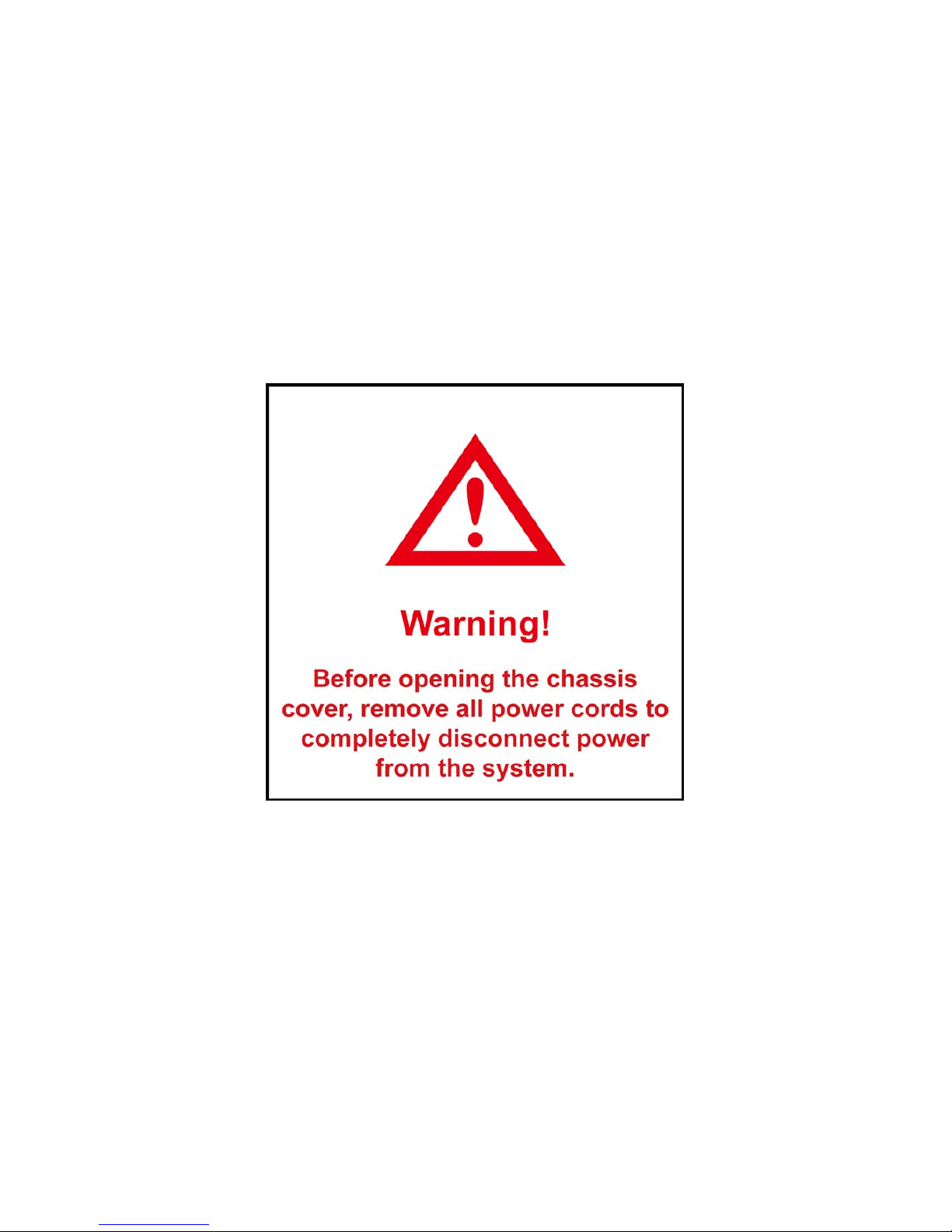
Warning: To reduce the risk of injury from electric shock, remove all power
cords to completely disconnect power from the system.
Weight in kg
Weight in lb
This symbol indicates that the component exceeds the recommended weight for
one individual to handle safely.
Warning: To reduce the risk of personal injury or damage to the equipment,
observe local occupational health and safety requirements and guidelines for
manual material handling.
Page 11

About This Manual
1230B0059901
iii
Safety Precautions
Observe the following safety precautions when you are connecting or disconnecting any device.
Regarding the standards of workstation regulations, do not place the server in the visual
field of the user, because of the glossy front of the case.
The product is non-consumer product and for profession technical person used only.
Operation Safety
Any operation on this server must be conducted by certified or experienced engineers.
Before operating your server, carefully read all the manuals included with the server
package.
Before using the server, make sure that all cables are correctly connected and power cords
are not damaged. If any damage is detected, contact your dealer as soon as possible.
To avoid short circuits, keep paper clips, screws, and staples away from connectors, slots,
sockets and circuitry.
Before opening the chassis panels, make sure all power cords are unplugged.
Avoid dust, humidity, and extreme temperatures; place the server on a stable surface.
If the power supply is broken, do not try to fix it by yourself. Contact an authorized dealer.
It is recommended that you wear gloves when assembling or disassembling the server to
protect from cuts and scrapes.
When the server is powered on, heat sinks and the surfaces of certain IC devices may be
hot. Do not touch them. Check whether the fans are functioning properly.
Make sure the four plastic feet are turned outward before setting the chassis down.
Electrical Safety
Before installing or removing signal cables, ensure that the power cords for the system unit
and all attached devices are unplugged.
To prevent electric shock hazard, disconnect the power cable from the electrical outlet
before relocating the system.
When adding or removing any additional devices to or from the system, ensure that the
power cords for those devices are unplugged before the signal cables are connected. If
possible, disconnect all power cords from the existing system before you add a device.
Use one hand, when possible, to connect or disconnect signal cables to prevent a possible
shock from touching two surfaces with different electrical potentials.
Page 12

About This Manual
1230B0059901
iv
This product is equipped with a three-wire power cable and plug for user safety. Use the
power cable with a properly grounded electrical outlet to avoid electric shock.
Motherboards, adapters, and disk drives are sensitive to static electricity discharge. These
devices are wrapped in antistatic bags to prevent this damage. Take the following precautions:
If you have an antistatic wrist strap available, use it while handling the device.
Do not remove the device from the antistatic bag until you are ready to install the device in
the system unit.
With the device still in its antistatic bag, touch it to a metal frame of the system.
Grasp cards and boards by the edges. Hold drives by the frame. Avoid touching the solder
joints or pins.
If you need to lay the device down while it is out of the antistatic bag. Lay it on the antistatic
bag. Before picking it up again, touch the antistatic bag and the metal frame of the system
unit at the same time.
Handle the devices carefully to prevent permanent damage.
Battery Replacement Safety
This server is provided with an internal Lithium battery or battery pack. There is a danger of
explosion and risk of personal injury if the battery is incorrectly replaced or mistreated.
For more information about battery replacement or proper disposal, contact an authorized reseller
or your authorized service provider.
This server contains an internal Lithium Manganese Dioxide, or a Vanadium Pentoxide, or an
alkaline battery pack. There is risk of fire and burns if the battery pack is not handled properly. To
reduce the risk of personal injury:
Do not attempt to recharge the battery.
Do not expose to temperatures higher than 70°C.
Do not disassemble, crush, puncture, shorten external contacts, or dispose in fire or water.
Replace only with the spare parts designated for this product.
Batteries should not be littered along with the general household waste. Please use the public
collection system or return them to the supplier.
Page 13

About This Manual
1230B0059901
v
Laser Peripherals or Devices Safety
To avoid risk of radiation exposure and/or personal injury:
Do not open the enclosure of any laser peripheral or device.
Laser peripherals or devices are not user serviceable.
Return to manufacturer for servicing.
Intended Application Uses
This product was evaluated as Information Technology Equipment (ITE), which may be installed in
offices, schools, computer rooms, and similar commercial type locations. The suitability of this
product for other product categories and environments (such as medical, industrial, residential,
alarm systems, and test equipment), other than an ITE application, may require further evaluation.
Site Selection
The system is designed to operate in a typical office environment. Choose a site that is:
Clean, dry, and free of airborne particles (other than normal room dust).
Well-ventilated and away from sources of heat including direct sunlight and radiators.
Away from sources of vibration or physical shock.
Isolated from strong electromagnetic fields produced by electrical devices.
In regions that are susceptible to electrical storms, we recommend you plug your system
into a surge suppresser and disconnect telecommunication lines to your modem during an
electrical storm.
Provided with a properly grounded wall outlet.
Provided with sufficient space to access the power supply cord(s), because they serve as
the product's main power.
Tools Required
A cross screwdriver or a flat screwdriver is needed to install or remove the components in the
server.
Page 14

About This Manual
1230B0059901
vi
Regulatory and Integration Information
Regulatory Compliance Identification Numbers
For the purpose of regulatory compliance certifications and identification, this motherboard is
assigned a serial number. This server serial number can be found on the product label, along with
the required approval markings and information. When requesting certification information for this
product, always refer to this serial number. This serial number should not be confused with the
marketing name or model number.
Product Regulatory Compliance
Worldwide Safety approvals can be supplied according to the requirements from Marketing or
Customer.
Product Safety Compliance
The motherboard complies with the following safety requirements:
Table i Product Safety Requirements
IEC 60950-1 Safety of Information Technology Equipment
EN 60950-1 Safety of Information Technology Equipment Including Electrical Business
Equipment, European Committee for Electrotechnical Standardization
(CENELEC)
UL 60950-1 Safety of Information Technology Equipment
UL 94 Tests for Flammability of Plastic Materials for Parts in Devices &
Appliances
GB4943 Safety of Information Technology Equipment
Product EMC Compliance
This product has been tested and verified to comply with the following electromagnetic
compatibility (EMC) regulations.
Communications Commission Notice
Part 15 of the Federal Communications Commission (FCC) Rules and Regulations has
established Radio Frequency (RF) emission limits to provide an interference-free radio frequency
spectrum. Many electronic devices, including computers, generate RF energy incidental to their
intended function and are, therefore, covered by these rules. These rules place computers and
related peripheral devices into two classes, A and B, depending upon their intended installation.
Class A devices are those that may reasonably be expected to be installed in a business or
commercial environment. Class B devices are those that may reasonably be expected to be
Page 15

About This Manual
1230B0059901
vii
installed in a residential environment (for example, personal computers). The FCC requires
devices in both classes to bear a label indicating the interference potential of the device as well as
additional operating instructions for the user.
The rating label on the device shows which class (A or B) the equipment falls into. Class A devices
do not have an FCC logo or FCC ID on the label. Class B devices have an FCC logo or FCC ID on
the label. Once the class of the device is determined, refer to the following corresponding
statement.
Class A Equipment
This equipment has been tested and found to comply with the limits for a Class A digital device,
pursuant to Part 15 of the FCC Rules. These limits are designed to provide reasonable protection
against harmful interference when the equipment is operated in a commercial environment. This
equipment generates, uses, and can radiate radio frequency energy and, if not installed and used
in accordance with the instructions, may cause harmful interference to radio communications.
Operation of this equipment in a residential area is likely to cause harmful interference, in which
case the user will be required to correct the interference at personal expense.
Declaration of Conformity for Products Marked with the FCC Logo—United States Only
This device complies with Part 15 of the FCC Rules Operation and is subject to the following two
conditions: (1) this device may not cause harmful interference, and (2) this device must accept any
interference received, including interference that may cause undesired operation.
For questions regarding your product, please contact the supplier.
To identify this product, refer to the Part, Series, or Model number found on the product.
European Union Notice
Products with the CE Marking comply with both the EMC Directive (89/336/EEC) and the
Low-Voltage Directive (73/23/EEC) issued by the Commission of the European Community.
Compliance with these directives implies conformity to the following European Norms (in brackets
are the equivalent international standards):
Table ii European Union EMC Requirements
EN55022 (CISPR 22) Electromagnetic Interference
EN55024 (IEC61000-4-2,3,4,5,6,8,11) Electromagnetic Immunity
EN61000-3-2 (IEC61000-3-2) Power Line Harmonics
EN61000-3-3 (IEC61000-3-3) Power Line Flicker
Page 16

About This Manual
1230B0059901
viii
Canadian Notice (Avis Canadien)
Class A Equipment
Japanese Notice
Taiwanese Notice
Page 17

Audience Assumptions
Manual Organization
Product Features
Motherboard Layout
System LED Information
Chapter 1
Introduction
Page 18

Introduction
1230B0059901
1-1
1 Introduction
1.1 Audience Assumptions
This document is for the person who installs, administers, and troubleshoots servers and
storage systems. IESC assumes you are qualified in the servicing of computer equipment and
trained in recognizing hazards in products with hazardous energy levels.
1.2 Manual Organization
This manual introduces the motherboard along with the hardware information and how to
replace the hardware. This manual is generally organized as follows:
Table 1-1 Manual Introduction
Introduction
General motherboard introduction and LED information.
Hardware Operations
The operation of the components on the motherboard, such as
system battery , processor, system memory, and so forth.
Connectors
Necessary information such as the locations and functions of the
connectors on the motherboard.
BIOS Setup
BIOS setup information.
Appendix
China RoHS Regulations information
Page 19
Introduction
1230B0059901
1-2
1.3 Product Features
This chapter provides the detailed features for processor, system memory, onboard LAN, D-sub
VGA, I/O and PCI with pictures for your reference.
Figure 1-1 Motherboard Overview
This motherboard dimension is designed for 12” x 17”. The motherboard is configured to use
Intel
®
5220 and Intel® 82801JIR chipset. It supports dual Intel® Nehalem-EP processors with
Intel
®
QuickPath Interconnect to accelerate even the most complicated server tasks. The
following highlights are the main features of the motherboard. For additional information, refer to
this user manual.
Table 1-2 Product Features
Processor
Intel
®
Nehalem-EP
Located on FCLGA 1366-pin socket
Chipset
Intel
®
5220
Intel
®
82801JIR
System Memory
18 240-pin DIMM vertical sockets
Supports unbuffered or registered DDR3 1066/1333MHz DIMMs
Supports up to 96GB (by Quad Rank RDIMM 12*8GB), or
144GB (by Dual Rank RDIMM 18*8GB) memory
Onboard LAN
Dual Gigabit Ethernet RJ45 port
Intel
®
82576 network controller
10/100/1000Mbps
Page 20
Introduction
1230B0059901
1-3
Management NIC: dedicate 10/100Mbps integrated in BCM5221
Onboard VGA
ASpeed AST2050
16MB DDR2 display memory
Integrated Super I/O
Winbond W83627HG controller
Supports 1 fast UART 16550 serial port, 1 PS/2 keyboard port,
and 1 PS/2 mouse port
Expansion Slot
2 expansion slots support:
Riser card for 1U Chassis with 1 slot.
1 PCI-E 2.0 slot (PCI-E 2.0 x16 speed with x16 slot)
1 PCI-E 2.0 slot (PCI-E 2.0 x8 speed with x8 slot)
Riser card for 2U Chassis with 3 or 2 slots.
2 PCI-E 2.0 slot (PCI-E 2.0 x8 speed with x16 slot) and 1
PCI-E 2.0 slot (PCI-E 2.0 x4 speed with x8 slot)
1 PCI-E 2.0 slot (PCI-E 2.0 x8 speed with x8 slot) and 1
PCI-E 2.0 slot (PCI-E 2.0 x2 speed with x4 slot)
Daughter Card
See Appendix A in the System User Manual
Expansion slot refers to the slot on the riser card. For more information, please see
System User Manual.
Page 21

Introduction
1230B0059901
1-4
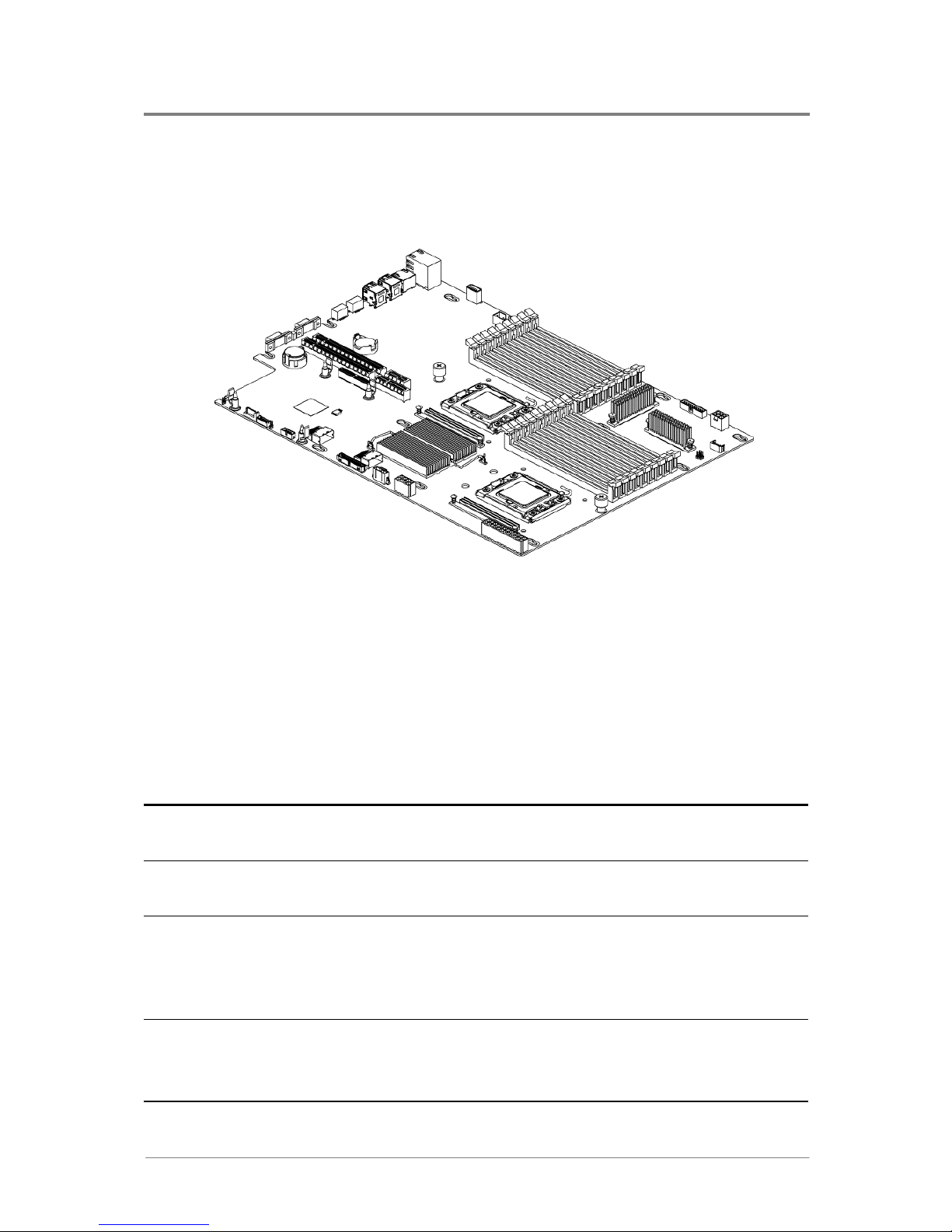
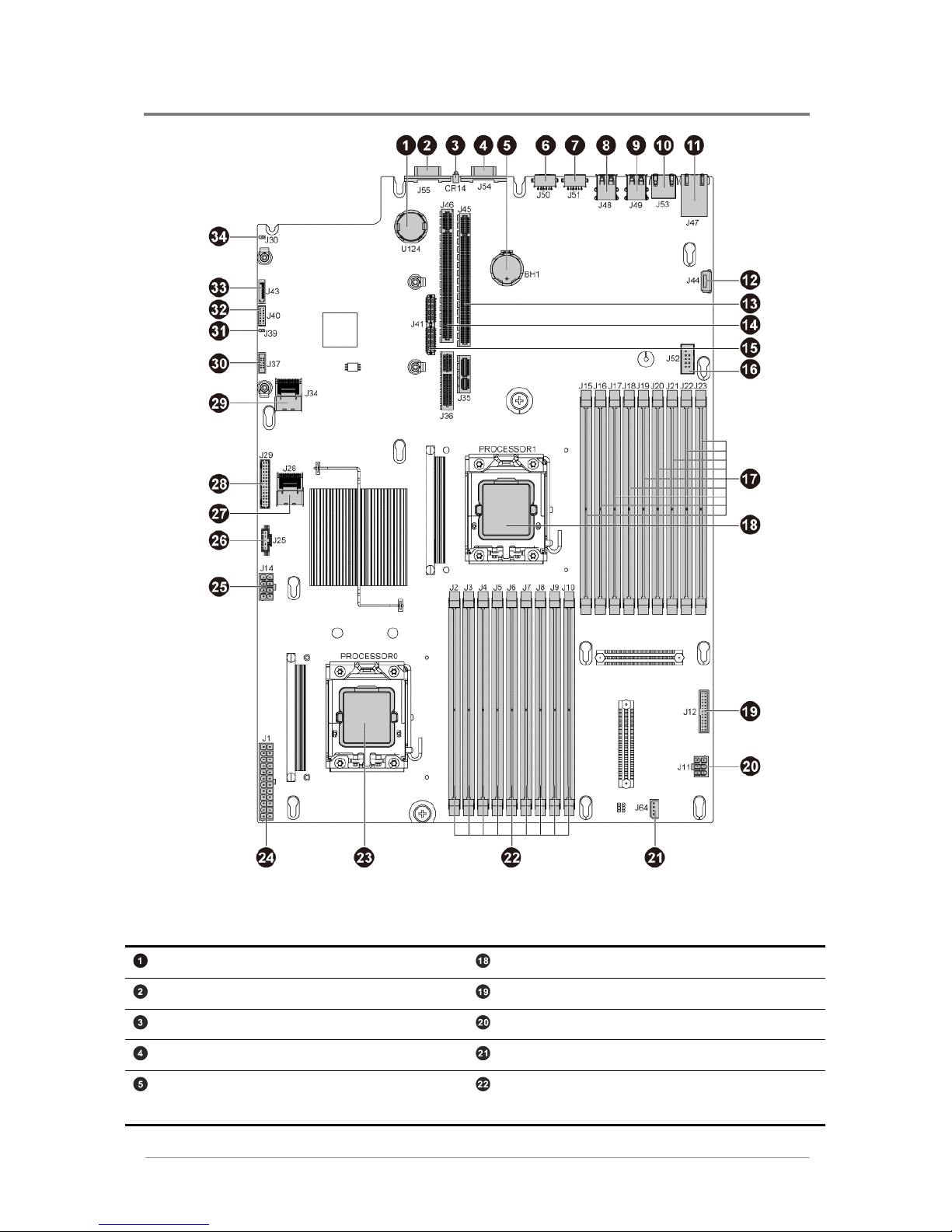
1.4 Motherboard Layout
The layout of the motherboard is shown below. Each connector and major component is
identified by the number.
1.4.1 Connectors and Component Locations
The words printed on the real motherboard to mark the processors are “CPU0” and
“CPU1”. Here just for consistency, the processors are marked with
“PROCESSOR0” and “PROCESSOR1” in the picture below.
Page 22
Introduction
1230B0059901
1-5
Figure 1-2 Connectors and Component Locations
I-button Socket (U124) Processor 1 (CPU1)
Serial Port (J55) System Fan Connector (J12)
ID (UID) LED (CR14) System Memory Power Connector (J11)
D-sub VGA Port (J54) IPMB Connector (J64)
System Battery (BH1) DIMM Sockets for Processor 0 (J2, J3, J4,
J5, J6, J7, J8, J9, J10)
Page 23
Introduction
1230B0059901
1-6
PS/2 Mouse Port (J50) Processor 0 (CPU0)
PS/2 Keyboard Port (J51) Main Power Connector (J1)
Rear Dual USB Port 1 (J48) Processor Power Connector (J14)
Rear Dual USB Port 2 (J49) I2C (SMBus) Signal Connector for Power
Supply (J25)
Management Port (RJ45) (J53) Mini-SAS Connector 2 (SATAII 4-5) (J28)
Dual NIC Connector (RJ45) (J47) Front Panel Connector (J29)
Internal USB Port (J44) Mini-SAS Connector 1 (SATAII 0-3) (J34)
Expansion Slot 2 (J45, J35) Front Panel USB Connector (J37)
Expansion Slot 1 (J46, J36) Chassis Intrusion Connector (J39)
PCI-E Daughter Card Connector (J41) Front Panel VGA Connector (J40)
USB Internal Connector (J52) SATA ODD Connector (J43)
DIMM Sockets for Processor 1 (J15, J16,
J17, J18, J19, J20, J21, J22, J23)
Management Engine Function Discovery
Jumper (J30)
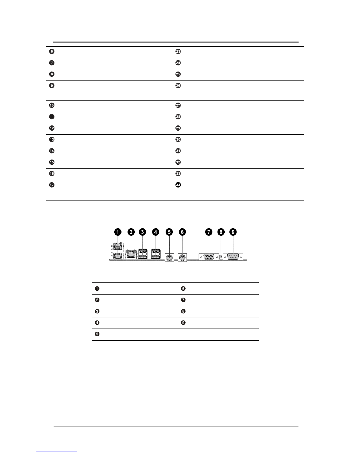
1.4.2 Back Panel Connectors
Figure 1-3 Back Panel Connectors
Dual NIC Connector (RJ45) PS/2 Mouse Port
Management Port (RJ45) D-sub VGA Port
Rear Dual USB Port 2 ID LED
Rear Dual USB Port 1 Serial Port
PS/2 Keyboard Port
Page 24
Introduction
1230B0059901
1-7
1.5 System LED Information
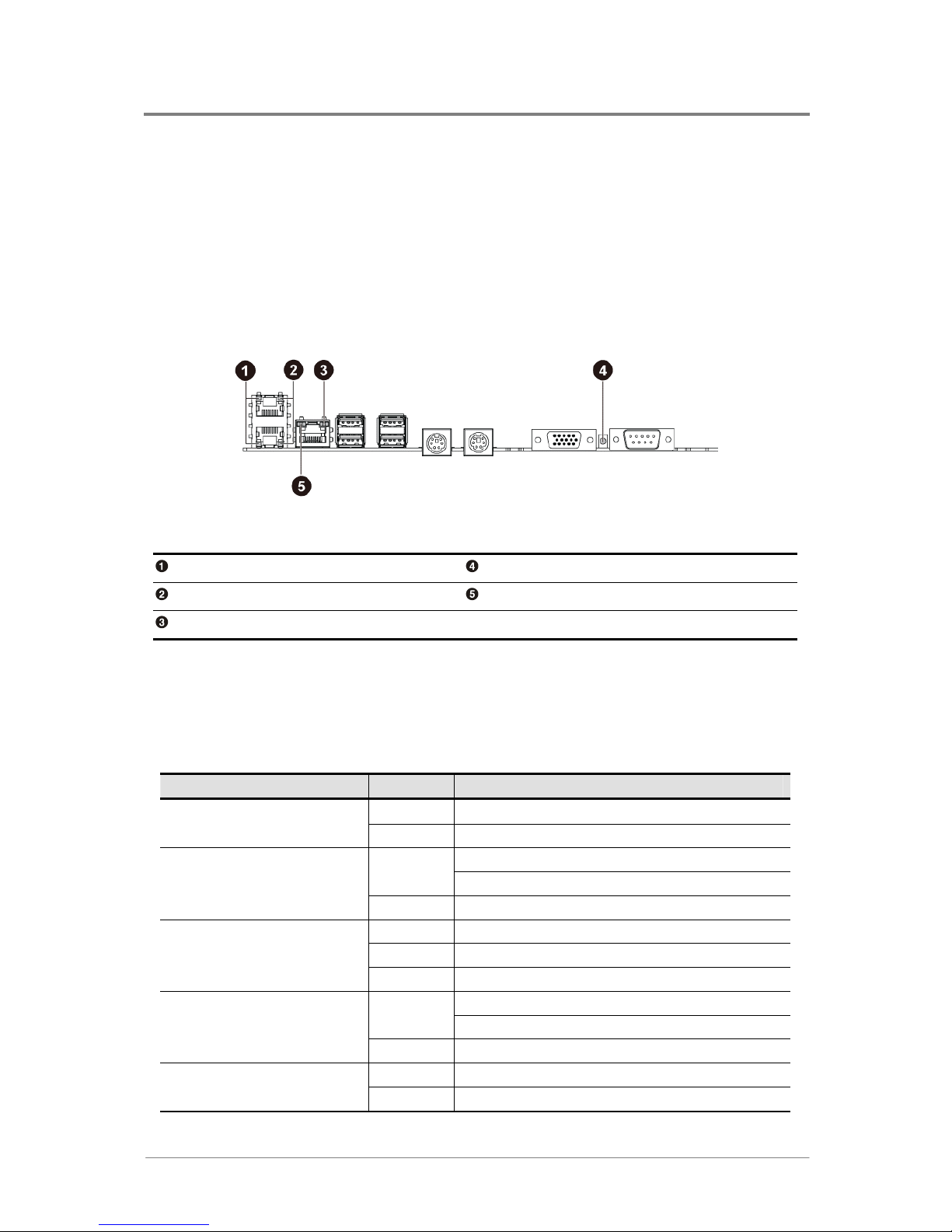
1.5.1 Back Panel LED Information
The back panel LED information displays details regarding the NIC LEDs, management port
LEDs and ID LED. Each NIC connector contains two LEDs that show the status of network
activity, link and speed.
Figure 1-4 Back Panel LEDs
NIC Link/Activity LED ID LED
NIC Speed LED Link/Activity LED of Management Port
Speed LED of Management Port
The detailed back panel LED information is shown below:
Table 1-3 Back Panel LED Information
Type of LED Color Status
Blue
On/Blinking: Chassis Identify
ID LED
−
Off: Disabled
On: Linking on
Green
Blinking: (At 1Hz rate) Accessing
NIC Link/Activity LED
−
Off: No link
Amber
On: Linking at 1Gbps speed
Green
On: Linking at 100Mbps speed
NIC Speed LED
−
Off: Linking at 10Mbps speed
On: Linking on
Green
Blinking: (At 1Hz rate) Accessing
Link/Activity LED of
Management Port
− Off: No link
Green
On: Linking at 100Mbps speed
Speed LED of
Management Port
−
Off: No connection/Linking at 10Mbps speed
Page 25

Introduction
1230B0059901
1-8
1.5.2 Front Panel LED Information
For the front panel LED information, please respectively refer to the 1U and 2U System User
Manual.
When the link/activity LED of management port is green and the speed LED of
management port is off, it means the speed LED is linking at 10Mbps; when both
the link/activity LED of management port and the speed LED of management port
are off, it means no connection for the management port.
Page 26

Before You Start
Screw Holes
System Battery
Processor
System Memory
Management Engine Function Discovery Jumper
Chapter 2
Hardware Operations
Page 27
Hardware Operations
1230B0059901
2-1
2 Hardware Operations
This chapter provides the detailed information and replacement steps for motherboard, including
system battery, processor and system memory.
2.1 Before You Start
Take note of the following precautions before you remove or install any components on the
motherboard.
The server does not completely power off when the front panel power button is pressed. The
button toggles server power between On and Hiberation. In Hiberation, the server removes
power from most electronics and drives, while portions of the power supply and some internal
circuitry remain active. To completely remove all power supplies from the system, disconnect
the power cords from the server.
Moving the Power On/Off switch to the Off position does not completely remove
system power. Some portions of the power supply and some internal circuitry remain
active. Disconnect all power cords from the server to remove all power from the
system.
To power off the server, please refer to “2.1.1 Power Off” in the System User Manual.
The components shown in this chapter are mainly for your reference. Please take
the actual shipment as standard.
To reduce the risk of injury from electric shock, remove the power cord to completely
disconnect power from the system.
Page 28

Hardware Operations
1230B0059901
2-2
2.2 Screw Holes
The motherboard is designed with totally thirteen locking tab holes and two thumbscrews as the
picture shows.
Figure 2-1 Screws Placement
Locking Tab Hole
Thumbscrew
Do not overly tighten the thumbscrews. Doing so may damage the motherboard.
Page 29

Hardware Operations
1230B0059901
2-3
2.3 System Battery
The location of system battery is shown below:
Figure 2-2 System Battery Location
Reminder
Before you remove or install the system battery, please follow the steps below:
Step 1:
Make sure the server is not turned on or connected to the AC power. To power off
the server, see “2.1.1 Power Off” in the System User Manual.
Step 2:
Remove the chassis cover. To remove the cover, see “2.2 Chassis Cover” in the
System User Manual.
Page 30
Hardware Operations
1230B0059901
2-4
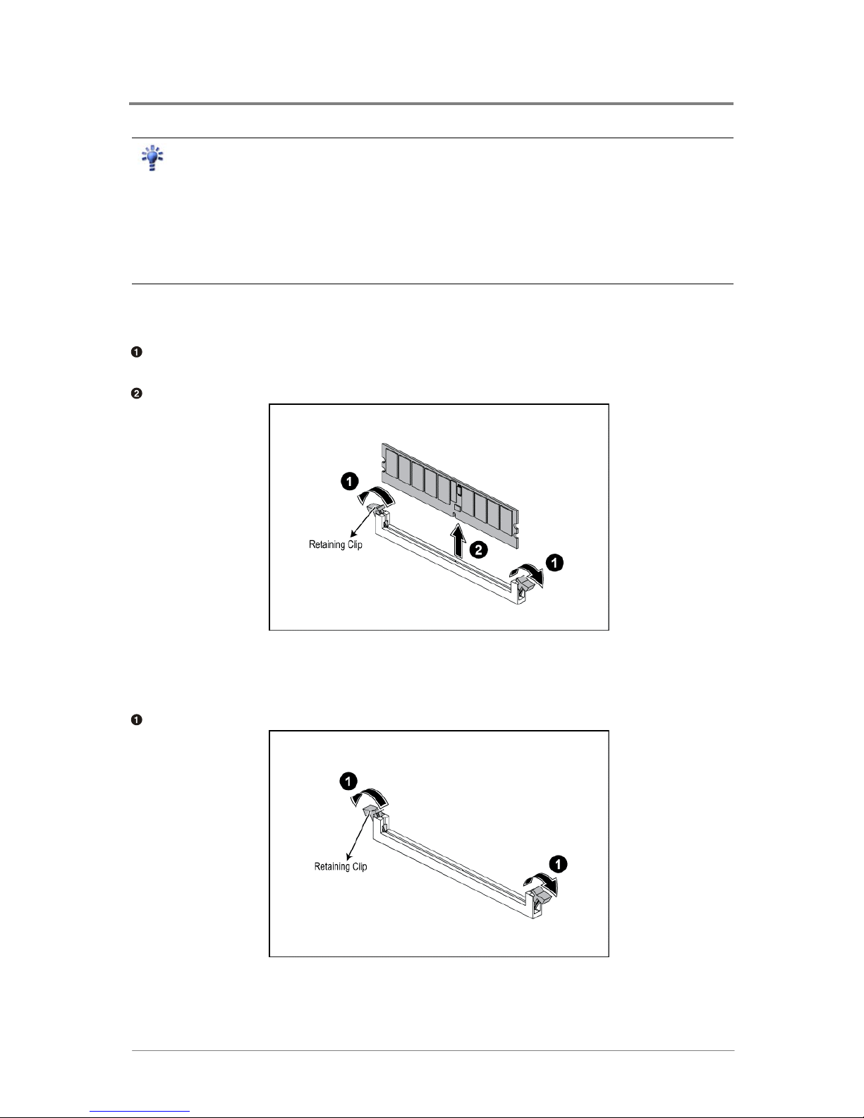
2.3.1 To remove the system battery
Squeeze the metal clamp.
Meanwhile, lift the system battery out of the holder.
Figure 2-3 Lifting the System Battery out of the Holder
2.3.2 To install the system battery
Slide one edge of the system battery under the holder’s lip with the positive side up. Push the
other edge down until the metal clamp snaps over the other edge of the system battery.
Figure 2-4 Putting the System Battery into the Holder
Page 31

Hardware Operations
1230B0059901
2-5
2.4 Processor
The motherboard supports dual Intel® Nehalem-EP processors. With two LGA 1366-pin sockets,
the system can be configured to either single or dual processors system.
The location of processors on the motherboard is shown below:
Figure 2-5 Location of Processors
Processor 0
Processor 1
You can install single or dual processors on the motherboard according to your own needs.
1. If SINGLE processor is intended, you must install the processor on the processor 0 socket,
please refer to the figure above.
2. If install DUAL processors, use the same type of processor running at the same frequency.
Page 32

Hardware Operations
1230B0059901
2-6
Reminder
Before you remove or install the heat sink or processor, please follow the steps below:
Step 1:
Make sure the server is not turned on or connected to the AC power. To power off
the server, see “2.1.1 Power Off” in the System User Manual.
Step 2:
Remove the chassis cover. To remove the cover, see “2.2 Chassis Cover” in the
System User Manual.
2.4.1 To remove the heat sink
Release the four screws.
Lift the heat sink up from the installed processor.
Figure 2-6 Removing the Heat Sink
Page 33

Hardware Operations
1230B0059901
2-7
2.4.2 To install the heat sink
Reverse the steps above to install the heat sink. When installing the heat sink, make sure to
position it in the direction where the ends of the heat sink fins face the front and back of the
chassis, as shown in the picture below, to allow proper airflow:
Figure 2-7 Positioning the Heat Sink to Allow Airflow
Before you put the heat sink on top of the installed processor, please do not forget to
check if the grease is complete on bottom of the heat sink.
2.4.3 To remove the processor
Unlock the load lever and lift it up.
Open the load plate.
Figure 2-8 Opening the Load Plate
Page 34
Hardware Operations
1230B0059901
2-8
Lift the processor out of the socket.
Figure 2-9 Lifting the Processor out of the Socket
Place the PnP cap onto the load plate.
Figure 2-10 Placing on the PnP Cap
Close the load plate.
Lock the load lever.
Figure 2-11 Locking the Load Lever
Page 35

Hardware Operations
1230B0059901
2-9
2.4.4 To install the processor
Reverse the steps above to install the processor. However, when inserting the processor into
the socket, make sure that the golden corner on the processor is pointed toward the socket as
picture shows:
Figure 2-12 Pointing the Golden Corner toward the Socket
When the processor is in place, press it firmly on the socket while you push
down the socket lever to secure the processor. The lever clicks on the socket
indicating that it is locked.
The processor fits only in one orientation. Do not force the processor into the
socket to avoid bending the pins and damaging the processor. If the processor
does not fit completely, check its orientation or check for bent pins.
Page 36

Hardware Operations
1230B0059901
2-10
2.5 System Memory
The motherboard supports eighteen unbuffered or registered DDR3 1066/1333MHz DIMMs to
provide up to 96GB or 144GB.
The location of DIMM sockets on the motherboard is shown below:
Figure 2-13 Location of the System Memories
There are eighteen DIMMs on the motherboard to support the processor 0 and processor 1. The
DIMM sequence of eighteen DIMM sockets is respectively shown below. When you insert the
DIMM(s), you have to always start with DIMM0 CH_A.
Page 37
Hardware Operations
1230B0059901
2-11
Table 2-1 DIMM Socket Location
Page 38

Hardware Operations
1230B0059901
2-12
For the installation options of each DIMM socket, please refer to the following table:
If only install one SINGLE processor, please refer to the following table to install the DIMMs.
Table 2-2 Unbuffered DIMM Installation Option for 1P Configuration
DIMM 2 DIMM 1 DIMM 0 DIMM2 DIMM1 DIMM 0 DIMM 2 DIMM
1
DIMM
0
DIMM Processor
CH_A CH_B CH_C
1 Processor 0 √
3 Processor 0 √ √ √
6 Processor 0 √ √ √ √ √ √
Table 2-3 Registered DIMM Installation Option for 1P Configuration
DIMM 2 DIMM 1 DIMM 0 DIMM2 DIMM1 DIMM 0 DIMM 2 DIMM
1
DIMM
0
DIMM Processor
CH_A CH_B CH_C
1 Processor 0 √
3 Processor 0 √ √ √
6 Processor 0 √ √ √ √ √ √
9 Processor 0 √ √ √ √ √ √ √ √ √
Page 39
Hardware Operations
1230B0059901
2-13
If install DUAL processors, please refer to the following table to install the DIMMs.
Table 2-4 Unbuffered DIMM Installation Option for 2P Configuration
DIMM 2 DIMM 1 DIMM 0 DIMM2 DIMM1 DIMM 0 DIMM 2 DIMM
1
DIMM
0
DIMM Processor
CH_A CH_B CH_C
Processor 0 √
2
Processor 1 √
Processor 0 √ √ √
6
Processor 1 √ √ √
Processor 0 √ √ √ √ √ √
12
Processor 1 √ √ √ √ √ √
Table 2-5 Registered DIMM Installation Option for 2P Configuration
DIMM 2 DIMM 1 DIMM 0 DIMM2 DIMM1 DIMM 0 DIMM 2 DIMM
1
DIMM
0
DIMM Processor
CH_A CH_B CH_C
Processor 0 √
2
Processor 1 √
Processor 0 √ √ √
6
Processor 1 √ √ √
Processor 0 √ √ √ √ √ √
12
Processor 1 √ √ √ √ √ √
Processor 0 √ √ √ √ √ √ √ √ √
18
Processor 1 √ √ √ √ √ √ √ √ √
The empty DIMM socket is marked as “”.
For the best performance, all the DIMMs installed must be at the same speed,
capacity and from the identical manufacturer.
Page 40
Hardware Operations
1230B0059901
2-14
Reminder
Before you remove or install any DIMMs, please follow the steps below:
Step 1:
Make sure the server is not turned on or connected to the AC power. To power off
the server, see “2.1.1 Power Off” in the System User Manual.
Step 2:
Remove the chassis cover. To remove the cover, see “2.2 Chassis Cover” in the
System User Manual.
2.5.1 To remove a DIMM
Unlock a DIMM socket by pressing the retaining clips outward. This action releases the
module and partially lifts it out of the socket.
Lift out the DIMM.
Figure 2-14 Lifting the DIMM out of the Socket
2.5.2 To install a DIMM
Unlock a DIMM socket by pressing the retaining clips outward.
Figure 2-15 Pressing the Retaining Clips Outward
Page 41

Hardware Operations
1230B0059901
2-15
Align the notch on the DIMM to the break on the socket. Carefully insert the DIMM into the
socket until the retaining clips snap back in place.
Figure 2-16 Inserting the DIMM into the Socket
DIMMs fit in only one direction. DO NOT force a DIMM into the socket to avoid
damaging the DIMM.
2.6 Management Engine Function Discovery Jumper
The motherboard involves one management engine function discovery jumper. The
management engine function discovery jumper is a two pin jumper (refer to “3.18 Management
Engine Function Discovery Jumper Setting”).
The location of management engine function discovery jumper on the motherboard is shown
below:
Figure 2-17 Management Engine Function Discovery Jumper Location
Page 42

Power Connectors
Front Panel Connector
Internal USB Port
USB Internal Connector
Chassis Intrusion Connector
IPMB Connector
Front Panel VGA Connector
D-sub VGA Port
Serial Port
Keyboard and Mouse Ports
Two Rear Dual USB Ports
Front Panel USB Connector
I
2
C (SMBus) Signal Connector for Power Supply
Dual NIC Connector (RJ45)
Management Port (RJ45)
System Fan Connector
SATA ODD Connector
Mini-SAS Connectors
Management Engine Function Discovery Jumper Setting
Chapter 3
Connectors and ME Function Discovery Jumper
Page 43

Connectors
1230B0059901
3-1
3 Connectors
The locations of all the connectors described in this chapter are shown in “1.4.1 Connectors
and Component Locations”.
“Key” stands for foolproof feature; “NC” stands for unused.
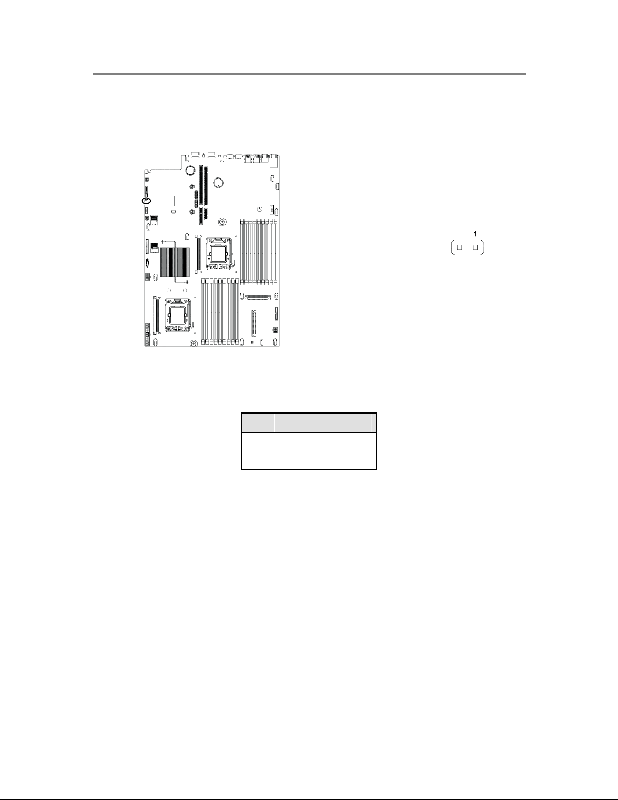
3.1 Power Connectors (J1, J14, J11)
The main power supply connection is obtained using the 24-pin connector.
The processor power supply connection is obtained using the 8-pin connector.
The system memory power supply connection is obtained using the 6-pin connector.
3.1.1 Main Power Connector (J1)
The 24-pin main power connector and the pin definition are shown below:
Figure 3-1 Main Power Connector
Page 44

Connectors
1230B0059901
3-2
Table 3-1 Main Power Connector Pin Definition
Signal Name Pin Pin Signal Name
+3.3V 1 13 +3.3V
+3.3V 2 14 -12V
Ground 3 15 Ground
+5V 4 16 DC_ON (Soft On/Off)
Ground 5 17 Ground
+5V 6 18 Ground
Ground 7 19 Ground
Power Good 8 20 NC
Stand By +5V 9 21 +5V
+12V 10 22 +5V
+12V 11 23 +5V
+3.3V 12 24 Ground
3.1.2 Processor Power Connector (J14)
The 8-pin processor power connector and the pin definition are shown below:
Figure 3-2 Processor Power Connector
Table 3-2 Processor Power Connector Pin Definition
Signal Name Pin Pin Signal Name
Ground 1 5 +12VA
Ground 2 6 +12VA
Ground 3 7 +12VB
Ground 4 8 +12VB
Page 45

Connectors
1230B0059901
3-3
The server will not boot if the 12V processor power connector is not attached to
the motherboard.
3.1.3 System Memory Power Connector (J11)
The 6-pin system memory power connector and the pin definition are shown below:
Figure 3-3 System Memory Power Connector
Table 3-3 System Memory Power Connector Pin Definition
Signal Name Pin Pin Signal Name
Ground 1 4 +12VD
Ground 2 5 Ground
Ground 3 6 Ground
Page 46

Connectors
1230B0059901
3-4
3.2 Front Panel Connector (J29)
The 30-pin front panel connector and the pin definition are shown below:
Figure 3-4 Front Panel Connector
Table 3-4 Front Panel Connector Pin Definition
Signal Name Pin Pin Signal Name
LED_POWER_BLINK 1 2 +3.3V_STBY
LED_HD_ACT_N 3 4 LED_FAIN_FAIL_N
LED_PF_UID_N 5 6 LED_SYS_HLTH_N
+5V_STBY 7 8 LED_NIC1_YELLOW_N
BTN_FP_PWR_N 9 10 LED_NIC2_YELLOW_N
BTN_FP_RST_N 11 12 LED_NIC1_ACT_BUF_N
BTN_FP_NMI_N 13 14 FP_I2C_SCL2
+5V 15 16 FP_I2C_SDA2
+5V 17 18 LED_NIC2_ACT_BUF_N
Ground 19 20 BTN_FP_UID_N
FP_I2C_SCL1 21 22 SYS_ID1
FP_I2C_SDA1 23 24 SYS_ID3
Ground 25 26 FP_I2C_ALERT_N
SYS_ID0 27 28 +3.3V_STBY
SYS_ID2 29 30 +5V
Page 47

Connectors
1230B0059901
3-5
3.3 Internal USB Port (J44)
The 4-pin internal USB port and the pin definition are shown below:
Figure 3-5 Internal USB Port
Table 3-5 Internal USB Port Pin Definition
Pin Signal Name
1 +5V_USB6_L
2 USB6_SB_L_DN
3 USB6_SB_L_DP
4 Ground
Page 48

Connectors
1230B0059901
3-6
3.4 USB Internal Connector (J52)
The 10-pin USB internal connector and the pin definition are shown below:
Figure 3-6 USB Internal Connector
Table 3-6 USB Internal Connector Pin Definition
Signal Name Pin Pin Signal Name
+5V_USB910_L 1 2 +5V_USB910_L
USB10_SB_L_DN 3 4 USB9_SB_L_DN
USB10_SB_L_DP 5 6 USB9_SB_L_DP
Ground 7 8 Ground
10 NC
Page 49
Connectors
1230B0059901
3-7
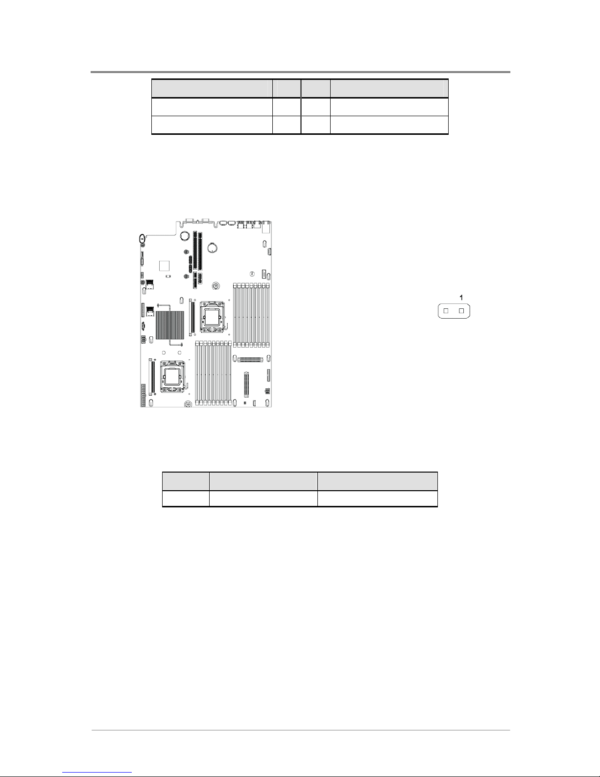
3.5 Chassis Intrusion Connector (J39)
The 2-pin chassis intrusion connector and the pin definition are shown below:
Figure 3-7 Chassis Intrusion Connector
Table 3-7 Chassis Intrusion Connector Pin Definition
Pin Signal Name
1 Intrusion Signal
2 Ground
Page 50

Connectors
1230B0059901
3-8
3.6 IPMB Connector (J64)
The 4-pin IPMB connector and the pin definition are shown below:
Figure 3-8 IPMB Connector
Table 3-8 IPMB Connector Pin Definition
Pin Signal Name
1 BMC_SDA7_+5V_IPMB
2 Ground
3 BMC_SCL7_+5V_IPMB
4 +5V_AUX
Page 51

Connectors
1230B0059901
3-9
3.7 Front Panel VGA Connector (J40)
The 14-pin front panel VGA connector and the pin definition are shown below:
Figure 3-9 Front Panel VGA Connector
Table 3-9 Front Panel VGA Connector Pin Definition
Signal Name Pin Pin Signal Name
RED 1 8 Horizontal Sync
Ground 2 9 Ground
GREEN 3 10 Vertical Sync
Ground 4 11 Ground
BLUE 5 12 SCL
Ground 6 13 SDA
Front VGA Use 7 14 Ground
Page 52

Connectors
1230B0059901
3-10
3.8 D-sub VGA Port (J54)
The 15-pin D-sub VGA port and the pin definition are shown below:
Figure 3-10 D-sub VGA Port
Table 3-10 D-sub VGA Port Pin Definition
Pin Signal Name
1 RED
2 GREEN
3 BLUE
4 NC
5 Ground
6 Ground
7 Ground
8 Ground
9 +5V
10 Ground
11 NC
12 SDA
13 Horizontal Sync
14 Vertical Sync
15 SCL
Page 53

Connectors
1230B0059901
3-11
3.9 Serial Port (J55)
The motherboard has one 9-pin serial port connector. The 9-pin serial port and the pin definition
are shown below:
Figure 3-11 Serial Port
Table 3-11 Serial Port Pin Definition
Pin Signal Name
1 DCD
2 RXDATA
3 TXDATA
4 DTR
5 Ground
6 DSR
7 RTS
8 CTS
9 RI
Page 54

Connectors
1230B0059901
3-12
3.10 Keyboard and Mouse Ports (J51, J50)
PS/2 keyboard and mouse ports are located on the back panel. The +5V lines to these ports are
protected with a PolySwitch* circuit that, like a self-healing fuse, reestablishes the connection
after an overcurrent condition is removed.
The PS/2 keyboard port and the pin definitions are shown below:
Figure 3-12 Keyboard Port
Table 3-12 Keyboard Port Pin Definition
Pin Signal Name
1 Keyboard Data
2 NC
3 Ground
4 +5V
5 Keyboard Clock
6 NC
Page 55
Connectors
1230B0059901
3-13
The PS/2 mouse port and the pin definition are shown below:
Figure 3-13 Mouse Port
Table 3-13 Mouse Port Pin Definition
Pin Signal Name
1 Mouse Data
2 NC
3 Ground
4 +5V
5 Mouse Clock
6 NC
The power to the server should be turned off before a keyboard or mouse is connected or
disconnected.
The keyboard and mouse controller contains the AMI keyboard and mouse controller code,
provides the keyboard and mouse control functions, and supports password protection for
power-on/reset. A power-on/reset password can be specified in the BIOS Setup program.
Page 56
Connectors
1230B0059901
3-14
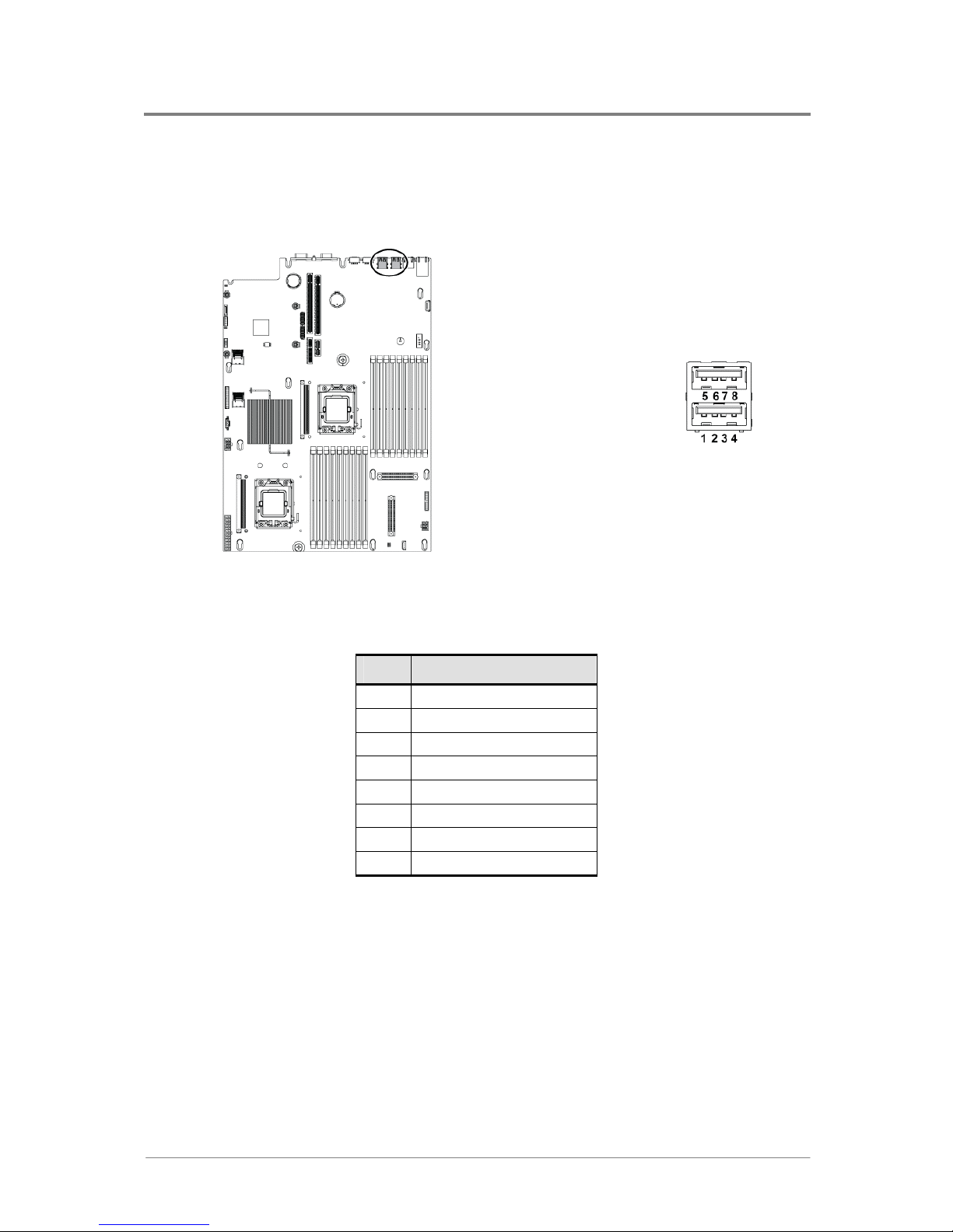
3.11 Two Rear Dual USB Ports (J48, J49)
The motherboard supports two rear dual USB ports. The rear dual USB port and the pin
definition are shown below:
Figure 3-14 Two Rear Dual USB Ports
Table 3-14 Rear Dual USB Port 1 Pin Definition (J48)
Pin Signal Name
1 +5V_USB34_L
2 USB4_SB_L_DN
3 USB4_SB_L_DP
4 Ground
5 +5V_USB34_L
6 USB3_SB_L_DN
7 USB3_SB_L_DP
8 Ground
Page 57

Connectors
1230B0059901
3-15
Table 3-15 Rear Dual USB Port 2 Pin Definition (J49)
Pin Signal Name
1 +5V_USB57_L
2 USB5_SB_L_DN
3 USB5_SB_L_DP
4 Ground
5 +5V_USB57_L
6 USB7_SB_L_DN
7 USB7_SB_L_DP
8 Ground
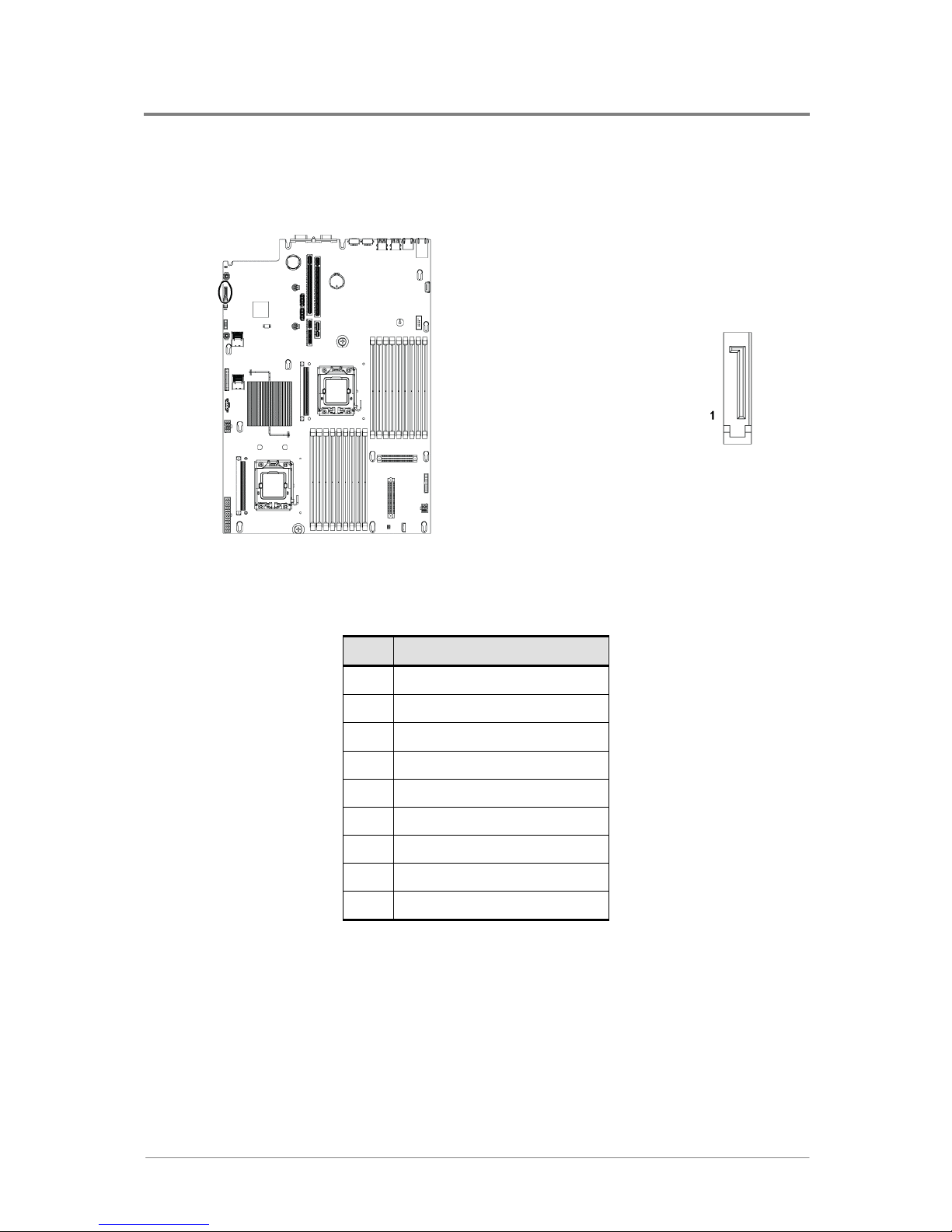
3.12 Front Panel USB Connector (J37)
A header on the motherboard provides an option to support one additional 10-pin USB
connector.
The 10-pin front panel USB connector and the pin definition are shown below:
Figure 3-15 Front Panel USB Connector
Page 58
Connectors
1230B0059901
3-16
Table 3-16 Front Panel USB Connector Pin Definition
Signal Name Pin Pin Signal Name
+5V_USB01 1 2 +5V_USB01
Ground 3 4 Ground
USB_IO0_DN 5 6 USB_IO1_DN
USB_IO0_DP 7 8 USB_IO1_DP
Ground 9 10 Ground
USB ports may be assigned as needed.
3.13 I2C (SMBus) Signal Connector for Power Supply (J25)
The 5-pin I2C (SMBus) signal connector for power supply and the pin definition are shown
below:
Figure 3-16 I
2
C (SMBus) Signal Connector for Power Supply
Table 3-17 I
2
C (SMBus) Signal Connector for Power Supply Pin Definition
Pin Signal Name
1 I2C SCL
2 I2C SDA
3 I2C Alert
4 Ground
5 +3.3V
Page 59
Connectors
1230B0059901
3-17
3.14 Dual NIC Connector (RJ45) (J47)
The motherboard supports a dual NIC connector (RJ45). The dual NIC connector is shown
below:
Figure 3-17 Dual NIC Connector (RJ45)
Table 3-18 Dual NIC Connector (RJ45) Pin Definition
Pin Signal Name
1 NIC_TX1+
2 NIC_TX13 NIC_RX1+
4 NIC_TX2+
5 NIC_TX26 NIC_RX17 NIC_RX2+
8 NIC_RX2-
Page 60

Connectors
1230B0059901
3-18
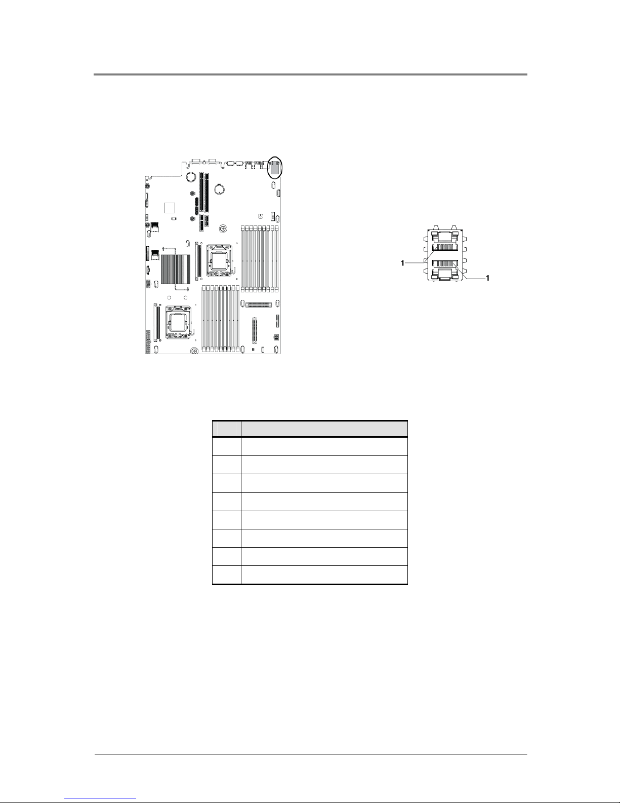
3.15 Management Port (RJ45) (J53)
The motherboard supports one management port (RJ45). The management port and the pin
definition are shown below:
Figure 3-18 Management Port (RJ45)
Table 3-19 Management Port (RJ45) Pin Definition
Pin Signal Name
1 Ethernet 10/100 Transmit+
2 Ethernet 10/100 Transmit3 Ethernet 10/100 Receive+
4 Unused
5 Unused
6 Ethernet 10/100 Receive7 Unused
8 Unused
9 N/A
10 N/A
11 Ground
12 Ground
13 SPEED LED+
14 SPEED LED15 LINKUP/ACTIVITY LED+
16 LINKUP/ACTIVITY LED-
Page 61

Connectors
1230B0059901
3-19
3.16 System Fan Connector (J12)
The 26-pin system fan connector and the pin definition are shown below:
Figure 3-19 System Fan Connector
Table 3-20 System Fan Connector Pin Definition
Signal Name Pin Pin Signal Name
FAN_BMC_TACH8 1 2 +3.3V_STBY
FAN_BMC_TACH7 3 4 FAN_CNTR_BUF_PWM1
FAN_BMC_TACH6 5 6 FAN_CNTR_BUF_PWM2
+3.3V 7 8 FAN_CNTR_BUF_PWM3
FAN_BMC_TACH4 9 10 FAN_CNTR_BUF_PWM4
FAN_BMC_TACH5 11 12 FAN_CNTR_BUF_PWM5
FAN_BMC_TACH3 13 14 Ground
FAN_BMC_TACH2 15 16 FAN_CNTR_BUF_PWM6
FAN_BMC_TACH1 17 18 I2C_SCL_FAN_CNTR_R
Ground 19 20 I2C_SDA_FAN_CNTR_R
FAN_BMC_TACH12 21 22 I2C_ALERT_FAN_N
FAN_BMC_TACH11 23 24 FAN_BMC_TACH9
FAN_BMC_TACH10 25 26 +5V
Page 62
Connectors
1230B0059901
3-20
3.17 SATA ODD Connector (J43)
The SATA ODD connector and the pin definition are shown below:
Figure 3-20 SATA ODD Connector
Table 3-21 SATA ODD Connector Pin Definition
Pin Signal Name
1 Ground
2 SATA_TX_C_DP
3 SATA_TX_C_DN
4 Ground
5 SATA_RX_C_DN
6 SATA_RX_C_DP
7 Ground
8 Ground
9 Ground
Page 63

Connectors
1230B0059901
3-21
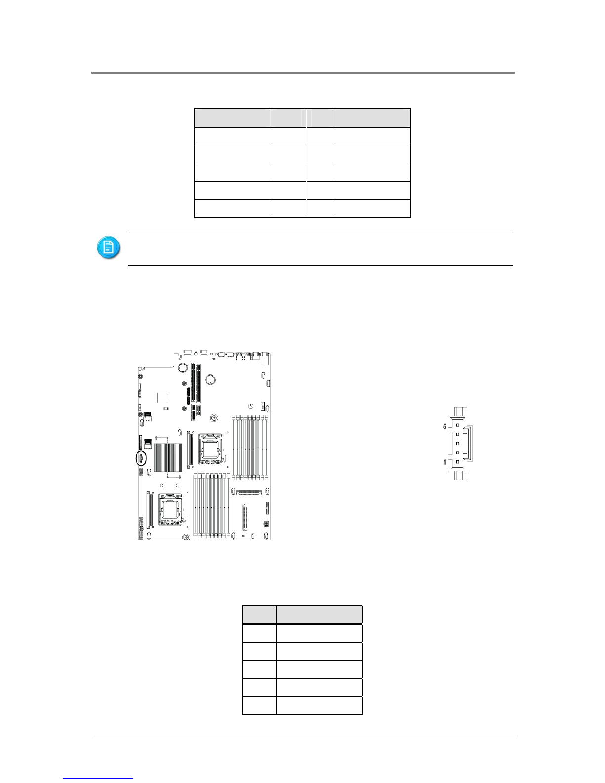
3.18 Mini-SAS Connectors (J34, J28)
The Mini-SAS connectors and the pin definition are shown below:
Figure 3-21 Mini-SAS Connector
Table 3-22 Mini-SAS Connector Pin Definition
Signal Name Pin Pin Signal Name
Ground B1 A1 Ground
SATA_TX1_C_DP B2 A2 SATA_RX1_C_DP
SATA_TX1_C_DN B3 A3 SATA_RX1_C_DN
Ground B4 A4 Ground
SATA_TX2_C_DP B5 A5 SATA_RX2_C_DP
SATA_TX2_C_DN B6 A6 SATA_RX2_C_DN
Ground B7 A7 Ground
SB_SATA_SCLK B8 A8 Key
SB_SATA_SLOAD B9 A9 Ground
Ground B10 A10 SB_SATA_SDO0
Ground B11 A11 SB_SATA_SDO1
Ground B12 A12 Ground
SATA_TX3_C_DP B13 A13 SATA_RX3_C_DP
SATA_TX3_C_DN B14 A14 SATA_RX3_C_DN
Ground B15 A15 Ground
SATA_TX4_C_DP B16 A16 SATA_RX4_C_DP
Page 64
Connectors
1230B0059901
3-22
Signal Name Pin Pin Signal Name
SATA_TX4_C_DN B17 A17 SATA_RX4_C_DN
Ground B18 A18 Ground
3.19 Management Engine Function Discovery Jumper Setting (J30)
The function of management engine function discovery jumper installed on motherboard is
shown below:
Figure 3-22 Management Engine Function Discovery Jumper
Table 3-23 Management Engine Function Discovery Jumper Function
Jumper Open Short
Pin 1-2 Normal (Default) ME_Disable
Page 65

BIOS Setup Utility
Entering the BIOS Setup Utility
Keyboard Command Bard
BIOS Updates
Chapter 4
BIOS Setup
Page 66

BIOS Setup
1230B0059901
4-1
4 BIOS Setup
This section describes the BIOS Setup Utility options. You can run BIOS Setup with or without
an operating system being present. Onboard devices are configured with the BIOS Setup utility
that is embedded in flash ROM.
The configuration utilities allow you to modify the CMOS RAM and NVRAM. The actual
hardware configuration is accomplished by the BIOS POST routines and the BIOS Plug-N-Play
auto-configuration manager. The configuration utilities update a checksum for both areas, so
potential data corruption is detected by the BIOS before the hardware configuration is saved. If
the data is corrupted, the BIOS requests that the user reconfigure the system and reboot.
Because the BIOS code is the most often changed part of the motherboard design,
the BIOS information described in this section may be a little different compared to
the actual BIOS that contained in your motherboard.
4.1 BIOS Setup Utility
This section describes the ROM-resident setup utility that provides the means to configure the
platform. The BIOS Setup utility is part of the system BIOS and allows limited control over
onboard resources.
The user can disable embedded PCI devices through the setup menus. When these devices are
disabled through setup, their resources are freed.
The following embedded devices can be disabled through setup menus, making them invisible
to a plug-and-play operating system that scans the PCI bus:
Onboard NIC 1 and NIC 2 embedded in Intel
®
82576
Onboard ASpeed AST2050 VGA
Page 67
BIOS Setup
1230B0059901
4-2
The BIOS options described in this section may or may not be present in
pre-production versions of the system BIOS. This section describes the BIOS utility
as it is planned to be at production and is subject to change. Option locations, in a
given menu of the BIOS Setup utility as described in this section, may be different
from those observed on any one pre-production version of the system BIOS.
The BIOS Setup utility screen is divided into four functional areas.
Table 4-1 BIOS Setup Utility Screen Description
Functional Area Description
Keyboard Command
Bar
Located at the bottom of the right screen or as
part of the help screen. This bar displays the
keyboard commands supported by the setup
utility
Menu Selection Bar
Located at the top of the screen. Displays the
various major menu selections available to the
user. The Server Setup utility major menus are:
Main Menu, Advanced Menu, Boot Menu,
Security Menu and Exit Menu
Options Menu
Each Option Menu occupies the left and center
sections of the screen. Each menu contains a set
of features. Selecting certain features within a
major Option Menu drops you into sub-menus
Item Specific Help
Screen
An item-specific Help screen is located at the
upside of the right side of the screen
4.2 Entering the BIOS Setup Utility
During the BIOS POST operation, the user is prompted to use the Del function key to enter
Setup as follows:
Press <Del> to run SETUP.
Press <Esc> to enter Diagnostic Messages. Then, press <F11> again to enter BBS POPUP.
A few seconds might pass before Setup is entered. This is the result of POST completing test
and initialization functions that must be completed before Setup can be entered. When Setup is
entered, the Main Menu options page is displayed.
Page 68
BIOS Setup
1230B0059901
4-3
4.3 Keyboard Command Bar
The right portion of the Setup screen provides a list of commands that are used to navigate
through the Setup utility. These commands are displayed at all times.
Each menu page contains a number of configurable options and/or informational fields.
Depending on the level of security in affect, configurable options may or may not be changed. If
an option cannot be changed due to the security level, its selection field is made inaccessible.
The Keyboard Command Bar supports the following:
Table 4-2 Keyboard Command Bar Description
Key Option Description
Enter
Execute
Command
The Enter key is used to activate sub-menus when the selected
feature is a sub-menu, or to display a pick list if a selected
option has a value field, or to select a sub-field for multi-valued
features like time and date. If a pick list is displayed, the Enter
key will undo the pick list, and allow another selection in the
parent menu.
ESC Exit
The ESC key provides a mechanism for backing out of any field.
This key will undo the pressing of the Enter key. When the ESC
key is pressed while editing any field or selecting features of a
menu, the parent me nu is r e-e nt ere d.
When the ESC key is pressed in any sub-menu, the parent
menu is re-entered. When the ESC key is pressed in any major
menu, the exit confirmation window is displayed and the user is
asked whether changes can be discarded. If “No” is selected
and the Enter key is pressed, or if the ESC key is pressed, the
user is returned to where they were before ESC was pressed
without affecting any existing settings. If “Yes” is selected and
the Enter key is pressed, Setup is exited and the BIOS
continues with POST.
↑
Select
Item
The up arrow is used to select the previous value in a pick list,
or the previous options in a menu item's option list. The selected
item must then be activated by pressing the Enter key.
↓
Select
Item
The down arrow is used to select the next value in a menu
item’s option list, or a value field’s pick list. The selected item
must then be activated by pressing the Enter key.
Page 69

BIOS Setup
1230B0059901
4-4
Key Option Description
← →
Select
Menu
The left and right arrow keys are used to move between the
major menu pages. The keys have no affect if a sub-menu or
pick list is displayed.
Tab
Select
Field
The Tab key is used to move between fields. For example, Tab
can be used to move from hours to minutes in the time item in
the main menu.
-
Change
Value
The minus key on the keypad is used to change the value of the
current item to the previous value. This key scrolls through the
values in the associated pick list without displaying the full list.
+
Change
Value
The plus key on the keypad is used to change the value of the
current menu item to the next value. This key scrolls through the
values in the associated pick list without displaying the full list.
On 106-key Japanese keyboards, the plus key has a different
scan code than the plus key on the other keyboard, but will
have the same effect
F9
Load
Optimal
Defaults
Pressing F9 causes the following to appear:
Setup Confirmation
Load Optimal Defaults?
[OK] [Cancel]
If “OK” is selected and the Enter key is pressed, all Setup fields
are set to their default values. If “Cancel” is selected and the
Enter key is pressed, or if the ESC key is pressed, the user is
returned to where they were before F9 was pressed without
affecting any existing field values.
Page 70

BIOS Setup
1230B0059901
4-5
Key Option Description
F10
Save and
Exit
Pressing F10 causes the following message to appear:
Setup Confirmation
Save Configuration changes and exit setup?
[OK] [Cancel]
If “OK” is selected and the Enter key is pressed, all changes are
saved and Setup is exited. If “Cancel” is selected and the Enter
key is pressed, or the ESC key is pressed, the user is returned
to where they were before F10 wa s pre ssed w ithou t a ffecting
any existing values.
4.4 BIOS Updates
4.4.1 BIOS Requirements
Table 4-3 BIOS Requirements Description
Utilities File Name Description
Flash BIOS Image
Under DOS
AFUDOS.EXE
ROM image file
FBB.BAT
AMIBIOS Flash Utility &
ROM image
Flash BIOS Image
Under Windows
AFUWIN.EXE
AMIBIOS Flash Utility &
ROM image
Recovery Mode AMIBOOT.ROM ROM image
Page 71

BIOS Setup
1230B0059901
4-6
4.4.2 ROM Flash
Update under DOS prompt
Copy AFUDOS.EXE, FBB.BAT and RomFileName.rom (ROM image) to bootable
storage.
Plug the bootable storage (ex: USB disk) and boot to DOS prompt (no HIMEM).
Specify the flash method depend on if Boot Block is needed to be updated.
FBB.BAT 1: Updates BIOS without Boot Block.
FBB.BAT 2: Updates BIOS with Boot Block.
Restart system & load BIOS default value.
Update under WinPE
Copy AFUWIN.EXE, UCORESYS.SYS, UCOREW64.SYS, and RomFileName.rom
(ROM image file) to the same directory.
Boot to WinPE and execute FBBWIN.BAT.
Restart system & load BIOS default value.
Recovery Mode
Prepare USB Disk on Key (or Floppy disk/CD-ROM) for recovery.
1) Format USB Disk on Key with FAT16/FAT32 format.
2) Copy RomFileName.rom and rename it to AMIBOOT.ROM.
Recovery method:
1) Press <Ctrl> + <Home> to invoke recovery function during POST.
2) Damage the ROM image, which will cause the system to enter recovery mode and update
the system ROM without the boot block.
3) Insert or plug-in the recovery media with the AMIBOOT.ROM file.
4) Power on system and wait for recovery process complete.
5) Restart system & load BIOS default.
Page 72

BIOS Setup
1230B0059901
4-7
4.4.3 BMC Flash
Update under DOS prompt
Copy rom.ima, KCSFLASH.EXE, F.BAT and RELEASE NOTE.doc to the bootable
storage (ex: USB).
Plug the bootable storage and boot to DOS prompt (no HIMEM).
Run F.bat to flash the BMC firmware.
BMC would be reset automatically after upgrade finished.
BMC Activate LED would be blinked after reset finished
Page 73

A
ppendix
China RoHS Regulations
Page 74
Appendix
1230B0059901
I
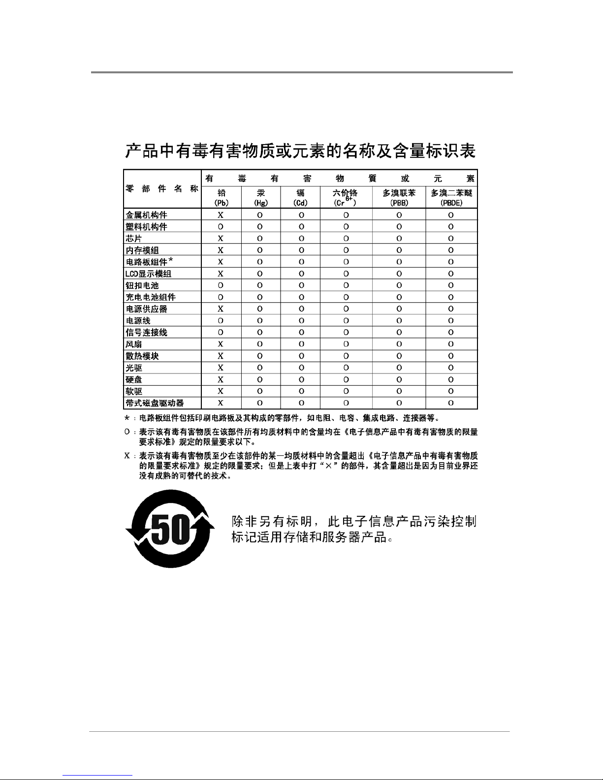
Appendix China RoHS Regulations
Appendix Figure I China RoHS Regulations
 Loading...