

Radio Shack TRS-80, TRS-80 4P Gate Array, 26-1080 Service Manual

•
ervlce
CUSTOM MANUFACTURED IN U.S.A. BY RADIO SHACK, A DIVISION OF TANDY CORPORATION

TRS-80"' Model 4Pi4P Gate Array Service Manual
Copyright" 1984 Tandy Corporation
All Rights Reserved.
Reproduction or use, without express written permission from Tandy Corporation. of any
in
portion of this manual is prohibited. While reasonable efforts have been taken
preparation of this manual to assure its accuracy, Tandy Corporation assumes no liability
resulting from any errors or omissions
contained herein.
in
this manual, or from the use of the information
the
TABLE OF CONTENTS
SECTION I
1.1
1.2
1.3
SECTION
2.1
2.2
2.3
2.4
2.5
SECTION
3.1
3.2
3.3
3.4
3.5
3.6
3.7
3.8
3.9
3.10
SECTION
Introduction. . . . . . . . . . . . . . . . . . . . . . . . . . . . . . . . . . . . . . . . . . . . . . . . . . . . . . . . . . . . . . . . . . . . . . . 1
SystemOverview
Optionai Features. . . . . . . . . . . . . . . . . . . . . . . . . . . . . . . . . . . . . . . . . . . . . . . . . .. . . . . . . . . . . . . . . . 3
System BlockDiagram. . . . . . . . . . . . . . . . . . . . . . . . . . . . . . . . . . . . . . . . . . . . . . . . . . . . . . . . . . . . . . 5
II
Specifications . . . . . . . . . . . . . . . . . . .. . . . . . . . . . . . . . . . . . . . . . . . . . . . . . . . . . . . . . . . . . . . . . . . . . 7
Microprocessor. . . . . . . . . . . . . . . . . . . . . . . . . . . . . . . . . . . . . . . . . . . . .. . . .. . . .. . . . . . . . . . . . . . .
Peripheral Interfaces. . . . . . . . . . . . . . . . . . . . . . . . . . . . . . . . . . . . . . . . . . . . . . . . . . . . . . . . . . . . . . . . 9
PowerRequirements 9
OperatingTemperature 9
Dimensions . . . . . . . . . . . . . . . . . . . . . . . . . . . . . . . . . . . . . . . . . . . . . . . . . . . . . . . . . . . . . . . . . . . . . . . 9
Disassembly/Assembly
III
Case
Internal Rear Mounting Plate.... . . . . . . . . . . . . . . . . . . . . . . .... . . . . . . . . . . . . . . . . . . . . . . . . ...13
FrontBezel. . . . . .
Top
Cover/Power
CathodeRayTube
CRTSweepBoard
Main Logic PCB. .. . . . . . . . . . . . . . . . . . . . . . . . . . . . . . . . . . . . . . . . . . . . . . . . . . . . . . . . . . . . . . . ...14
KeyboardAssembly . . . . . . . . . . . . . . . . . . . . . . . . . . . . . . . . . . . . . . . . . . . . . . . . . . . . . . . . . . . . . ...14
DiskDriveAssembly. . . . . . . . . . . . . . . . . . . . . . . . . . . . . . .... . . . .
Control Module .. . . . . . . . . . . . . . . . . . . . . . . . . . . . . . . 15
IV
Maintenance/Troubleshooting (general suggestions, reference
to section below for specific troubleshooting hints) . . . . . . . . . . . . . . . . . . . . .. . . . . . . . . . . . . . .
..
.. . . . . . . . . . . . . . . . . . . . . . . . . . . . . . . . . . . . . . . . . . . . . . . . . . . . . . . . . . . . . . . 3
..
.. . . . .... . . . . . . . . . . . . . . . . . . . . . . .....
Supply....
. . . . . .... . . . . .... . . . . . . .... . . . . . . . . . . . . .... . . . . . . . . .....
. . . . . . . . . . . . . .
.. ..
.. ......
.. ..... . . . . ...13
. .
.. ..
11
13
13
14
14
. . . . . ...15
..
17
9
SECTION V
5.1
5.1.1
5.1.2
5.1.3
5.1.4
5.1.5
5.1.6
5.1.7
5.1.8
5.1.9
5.1.10
5.1.11
5.1.12
5.1.13
5.1.14
5.1.15
5.1.16
5.1.17
5.2
5.2.1
5.2.2
5.2.3
4P
Theory of Operation . . . . . . .... . . . . . . . . . . . . . . . . . . . . . . . . . . . . . . . . . . . . . . .
CPU Theory ofOperation
Introduction. . . . . . . . . . . . . . . . . . . . . . . . . . . . . . . . . . . . . . . . . . . . . . . . . . . . . . . . . . . . . . . . . . . . ...23
ResetCircuit .. . . . . . . . . . . . . . . . . . . . . . . . . . . . . . . . . . . . . . . . . . . . . . . . . . . ...23
CPU............................................................................
SystemTiming. . . . . . . . . . . . . .. . . . . . . . . . . . . . . . . . . . . . . . . . . . . . . . . . . . . . . . . . . . . . . . .
AddressDecode . . . . . . . . . . .... . . . . . . . . . . . . . . . . . . . . ..... . . . . . . . . . ..... . . .. . . . . . . .
ROM.......................................................................
RAM
VideoCircuit
Keyboard... . . . . . . . . . . . . . . . . . . . . . . . . . . .... . . . . . . . . . . . . . . ..... . . . . . . . . . . . . . . . . . . .
Real Time Clock . . . . . . . . . . . . . . . . . . . . . . . . .. . . . . .... . . . . .
LinePrinterPort. . . . . .... . . . . . . .... . . . . . . . . . . . . ..... . . . .... . . . . . . . . . . . . . . . . . . . . . . .
GraphicsPort. . . . . . . . . . . . . . . . . . . . . . . . . . . . . . . . . . . . . . . . . . . . . . . . . . . . . . . . . . . . . . . . . . . ...57
Sound
I/OBusPort
FDCCircuit 59
RS-232CCircuit 64
Troubleshooting (specific)
Schematic8000192 . . . . . . . . . . . . . . . . . . . . . . . . . . . . . . . . . . . . . . . . . . . . . . . . . . . . . . . . . . . . . . .
PCBArt(1700254)
Parts List, PCB Assembly .. . . . . . . . . . . . . . . . . . . . . . . . . . . . . . . . . . . . . . . . . . . . . ...79
4P Gate Array Theory of Operation . . . . .... . . .... . . . . . . . . . . . . . . . . . . . . . . . . . . . . . . . . .
CPU Theory of Operation
Introduction. . . . . . . . . . . . . . . . . . . . . . . . . . . . . . . . . . . . . . . . . . . . . . . . . . . . . . . . . . . . . . . . . .
ResetCircuit .. . . . . . . . . . . . . . . . . . . . . . . . . . . . . . . . . . . . . . . . . . . ...85
C~
.. ..
. . . . . . . . . . . . . . . . . . . . . .
····
.. ..
. . . . . ...21
...
..
..
..
.. ..
·····85
23
23
23
26
26
37
51
53
53
53
57
57
66
67
75
85
85
85
5.2.4
5.2.5
5.2.6
5.2.7
5.2.8
5.2.9
5.2.10
5.2.11
5.2.12
5.2.13
5.2.14
5.2.15
5.2.16
5.2.17
5.3
5.4
5.4.1
5.4.2
5.4.3
5.4.4
5.4.5
5.4.6
5.4.7
5.5
5.5.1
5.5.2
5.5.3
5.6
5.6.1
SystemTiming. . . . . . . . . . . . . . . . . . . . . . . . . . . . . . . . . . . . . . . . . . . . . . . . . . . . . . . . . . . . . . . . . . .
_AddressDecode . . . . . . .... . . . . . . .... . . . . .... . . . . . . .... . . . . . . . . . . . . . . . . . . . . . . . . . . 87
ROM 87
RAM 98
VideoCircuit 112
Keyboard . . . . . . . . . . . . . . . . . . . . . . . . . . . . . . . . . . . . . . . . . . . . . . . . . . . . . . . . . . . . . . . . . . . . . . .
..
RealTime Clock . . . . . . . . .
Line PrinterPort
GraphicsPort 118
. . . . . . . . . . . . . . . . . . . . . . . . . .... . . . . . . . . . . . . . .... . . . . . . . ...114
_.. . . . . . . . . . . . . . . . . . . . . . . . . . . . . . . . . . . . . . .
.. ..
..
85
..
114
. ...114
Sound 118
110
Bus Port 118
FDCCircuit 120
RS-232CCircuit 124
Troubleshooting(specific) 126
Schematic8000192
Art (1700254) _ 134
PCB
Parts List, PCB Assembly . . . . .
Mini-Disk Drives
PowerSupplyAssembly 143
PowerSupplyDescription .. . . . . . . . . . . . . . . . .
Technical Specifications 147
Theoryof Operation . . . . . . . . . . . . . . . . . . . . . . . . . . . . . . . . . . . . . . . . . . . . . . . . . . . . . . . . . . . . . .
TroubleshootingChart
Testingand Adjustments
Schematic 8000164, 65W Power Supply 8790049
Component Layout, 65W Power Supply 8790049 . . . . . . . . . . . . . . . . . . . . . . . . . . . . . . . . . . . . ...163
Circuit Trace, 65W Power Supply 8790049 . . . . . . . . . . . . . . . . . . . . . . . . . . . . . . . . . . . . . . . . . . .
Parts List, 65W Power Supply 8790049
CRTDisplay
Specifications
Adjustmentprocedures
Theoryof Operation . . . . . . . . . . . . . . . . . . . . . . . . . . . . . . . . . . . . . . . . . . . . . . . . . . . . . . . . . . . . . ...174
Schematic 23533 (BIW) and 23757 (Green) 179
Parts list 8790612 (BIW) and 8790613 (Green)
Options 189
GraphicsBoard 189
(Tan
_ 127
..
. . . . .... . . . . . . . . . . . . . . . . . . . . . . . . ......137
don TM-50) 143
..
. . . .... . . . . . . . . . . . . . . . . . . . . . . . . . . ......143
..
148
_.. . . . . . . . . . . . . . . . . . . . . . . . . . . . . . . . . . . . . . . . . . . . . ...158
_ " 159
161
..
164
_ " 165
_........
_
. _ 169
_ 169
171
181
SECTION
ADDENDA
A.
VI
Exploded View/Parts
CaseAssembly . 202
Main ChassisAssembly
DiskDriveAssembly 206
KeyboardAssembly
Tandon Operating and Service Manual,
Lists.
. . . . . . . . 199
_ _ _ 204
_. . _ 208
TM50-1 and TM50-2 5-1/4" Flexible Disk Drives
MODEL 4P/4P GATE ARRAY
HARDWARE
SECTION I
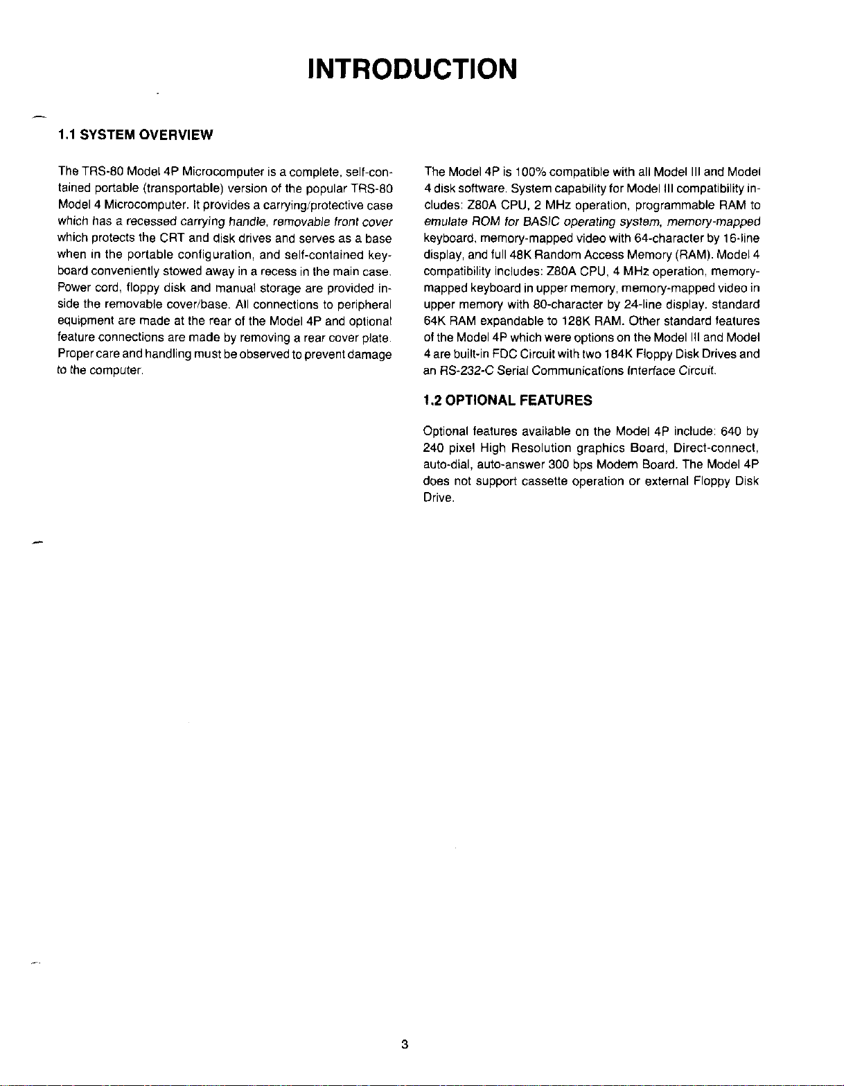
INTRODUCTION
INTRODUCTION
1.1
SYSTEM OVERVIEW
The
TRS-SO
tained portable (transportable) version of the popular
Model 4 Microcomputer.Itprovides a carrying/protective case
which
which protects the CRT and disk drives and serves as a base
when in the portable configuration, and self-contained key-
board
Power cord, floppy disk and manual storage are provided in-
side
the
equipment are made at the rear of the Model 4P and optional
feature
Proper care and handling must be observed to prevent damage
to
the
Model4P
hasarecessed
conveniently
removable
connections
computer.
Microcomputerisa complete, self-con-
carrying
stowed
cover/base.
are
handle,
awayina
madebyremovingarear
removable
recessinthe
All
connectionstoperipheral
front
main
cover
TRS-SO
cover
case.
plate.
The Model 4Pis100% compatible with all Model
4 disk software. System capability for Model III compatibility includes:
emulate ROM
keyboard, memory-mapped video with 64-character by 16-line
display, and full
compatibility includes:
mapped keyboard
upper memory with SO-character by 24-line display, standard
64K
of the Model4P which were options on the Model
4 are built-in FDC Circuit with two
an
ZSOA
CPU, 2 MHz operation, programmable RAM to
lor
BASIC operating system, memory-mapped
4SK
Random Access Memory (RAM). Model 4
ZSOA
CPU, 4 MHz operation, memory-
in
upper memory, memory-mapped video in
RAM
expandable to 12SK RAM. Other standard teatures
lS4K
Floppy Disk Drives and
RS-232-C Serial Communications Interface Circuit.
III
and Model
III
and Model
1.2 OPTIONAL FEATURES
Optional features available on the Model 4P include: 640 by
240 pixel High Resolution graphics Board, Direct-connect,
auto-dial, auto-answer 300 bps Modem Board. The Model 4P
does not support cassette operation
Drive.
or
external Floppy Disk
3
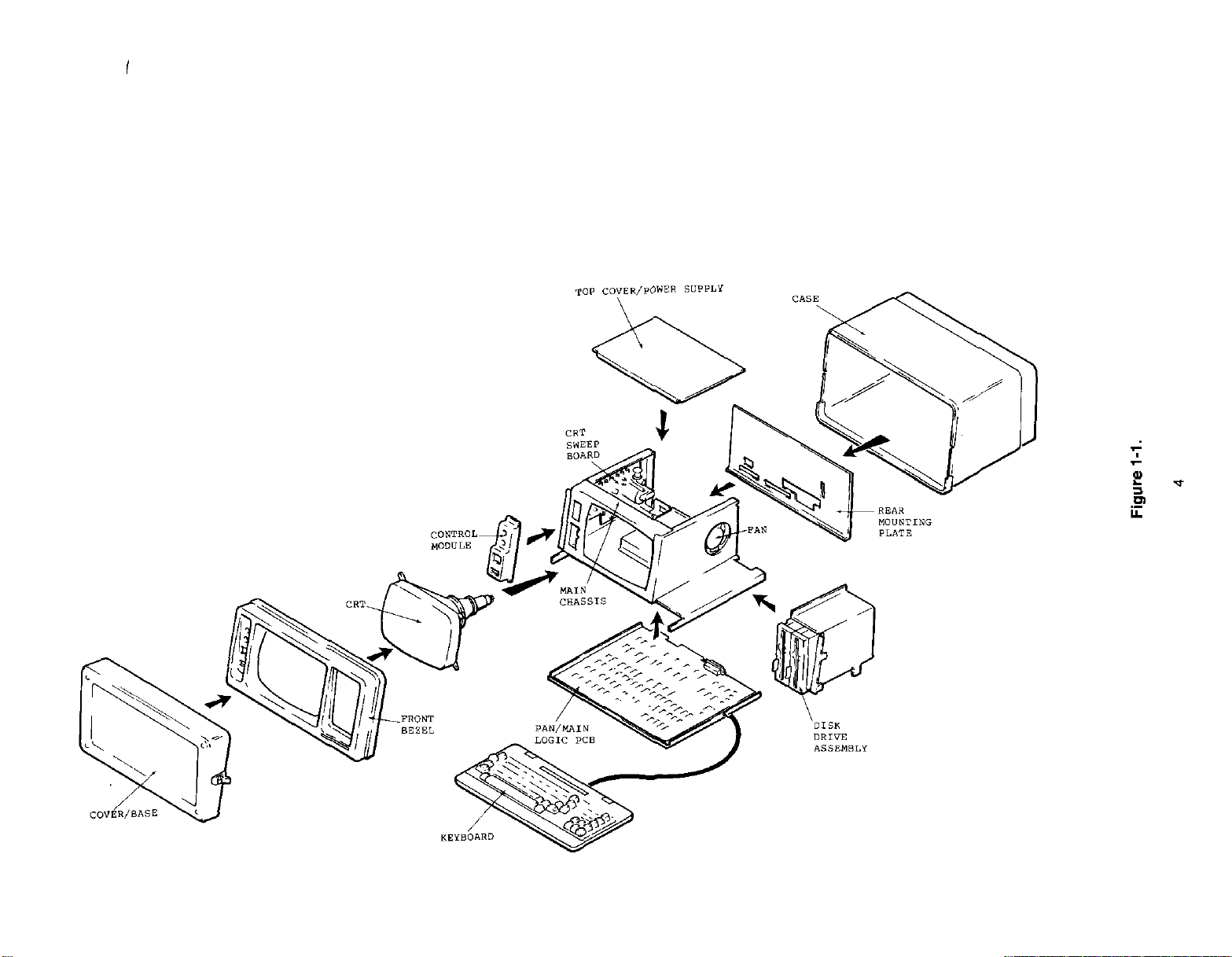
TOP
COVER/POWER
,~
SUPPLY
CASE
~"
COVER/BASE
CONTROL
MODULE
,"
~~j'"
1>1
11
~~MAIN
FRONT
BEZEL
KEYBOARD
CRT
SWEEP
BOARD
1'l/$
lJ
Uo
CHASSIS
PAN/MAIN
LOGIC
PCB
~
DISK
DRIVE
ASSEMBLY
REAR
MOUNTING
PLATE
~
~
ii:
,
l!!
:::>
Dl
"
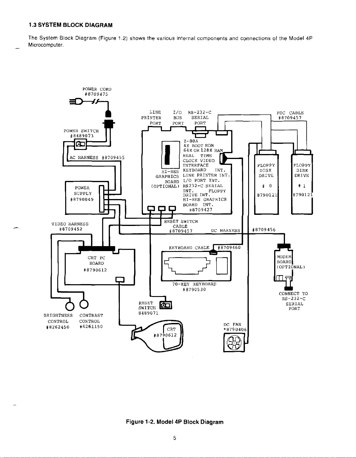
1.3 SYSTEM BLOCK DIAGRAM
The System Block Diagram (Figure 1.2) shows the various internal components and connections of the Model 4P
Microcomputer.
POWER
CORD
#8709475
50---4'
#8709455
POWER
SUPPLY
#8790049
VIDEO HARNESS
#8709452
CRT
PC
BOARD
iB790612
LINE
PRINTER
PORT
GRAPHICS
(OPTIONAL)
I/O
BUS
PORT
~~8~~OT
64KOR128K
REAL
[J
HI
BOARD
RESET
CLOCK
INTERFACE
- RES KEYBOARD
LINE
r/o
RS232-c
INT.
DRIVE
HI-RES
BOARD
SWITCH
CABLE
#8709457
KEYBOARD
RS-232-C
SERIAL
PORT
TIME
VIDEO
PRINTER
PORT
INT.
INT.
#8709427
CABLE
ROM
RAM
INT.
INT.
INT.
SERIAL
FLOPPY
GRAPHICS
DC
HARNESS
#8709460
FOC
CABLE
#8709457
..
__
..
FLOPPY
DISK
DRIVE
# 0
8790121
#8709456
FLOPPY
DISK
DRIVE
# 1
8790121
BRIGHTNESS
CONTROL
#8262450
CONTRAST
CONTROL
#8261150
RESET
SWITCH
8489071
#87D
70-KEY
E1
KEYBOARD
iB790530
Figure 1-2. Model4PBlock
5
Diagram
DC
FAN
*8790406
CONNECT
RS-232-c
SERIAL
PORT
TO

SECTION
II
SPECIFICATIONS
7
SPECIFICATIONS
2.1
MICROPROCESSOR: 4 MHz Z80A, 8-bit CPU
Memory:
Keyboard:
Video Display:
Floppy Disk Drives:
64K RAM bytes, expandable
70-key standard typewnter keyboard, including 12-key numeric entry keypad. Special keys include
BREAK, CTRL, CAPS, CLEAR, plus three programmable special function keys (F1, F2, and F3).
High-resolution
Model
III
and lower case ASCII characters, with descenders, 96 special characters, 64 alternate characters,
64 graphics characters, plus reverse video of
Two built-in single-sided, double-density
184K bytes. Data transfer rate
2.2 PERIPHERAL INTERFACES
Standard:
Optional:
I/O BUS for connection of hard disk and other peripherals.
Serial Interface (RS-232-C port) One RS-232-C Serial Communications
asynchronous
4P.
Parallel
Model4P.
640 x 240 High-Resolution graphics board
to
128K bytes 4K boot ROM, 2K video memory
9"
black and white display monitor with 64 or 32 characters per line by 16 lines
mode and 80 or 40 characters per line by 24 linesinModel 4/4P mode. Displays upper
all
ASCII alpha-numeric characters.
5-114"
thin-line floppy disk drives. Each drive stores up to
is
250K bits per second.
Interface port which allows
and
Printer
synchronous
Interface
transmission.
Connectiontoa
line
Mates
printer
with
via
08-25
the
connectoronbackofthe
34-pin
connectoronthe
Model
backofthe
in
Auto-answer Modem (300 baud)
2.3 POWER REQUIREMENTS
105-130 Vac, 60 Hz
240 Vac, 50 Hz (Australian)
220 Vac, 50 Hz (European)
Grounded Outlet
Maximum
Typical Current Drain: 1.5 Amperes
Current
Drain:
1.7
Amperes
2.4 OPERATING TEMPERATURE: 55 to 80
2.5 DIMENSIONS: 9.3" H x 16.5" W x 13.25"
0
F (13 to2TC)
D,
261bs carrying weight.
9
SECTION III
DISASSEMBLY/ASSEMBLY
11
DISASSEMBLY/ASSEMBLY
3.1
OVERVIEW AND CASE
The
Model4Pismodularinconstructioninthatitcanbedisas-
sembledinmajor
cover. These major component blocks include the disk drives,
the power supply, main CPU board, the CRT display, and the
monitor
additional diskettes, and operating manual can be stored
convenient recessesinthe removable
cover/base provides protection for the CRT and disk drives during
sitionofthe
The cover/baseisheld in place with snap locksoneach side.
These
vent
unsnap the lock and release the catch from the main assembly
latch. The following procedures are noted in sequential order
requiredtoprovide
parts
are
instructions.
1.
board.
transport.Italso serves as the baseinthe non-operating po-
locks
accidental
removal
noted.
The main
cover
which
removed.
These include theACpower cord, printer cable, I/O port
connector, and RS-232-C connector. The printer cable and
I/O port connectors are edge card type connectors
ercise
component
Accessory
computer.
are
positive
openingofthe
accesstosomeofthe
does
not
require
For
reassemblyofunit,
assembiy
allows
accesstoall
Remove
careintheir
removal.
blocks
after
removalofthe
components
action
cover/base.Toremove,
previous
of the Model 4P has a removable
all
connectionstothe
suchasthe
front
cover/base. This
withaprotective
components.
steps.
Those
reverse
orderofdisassembly
internal
components
rearofthe
power
bosstopre-
merely
which
case
cord,
Some
do
when
unit.
- ex-
side of the unit. With the rear of the unit toward you, two of
in
these screws are located at the left just
Drive Assembly and accessibie from the left side of the
chassis
the rear of the chassis assembly.
3.
in
Six other screws are located around the outside edges of
the rear mounting plate. Remove the plate and set
for reassembly.
assembly.
The
twoonthe
right
front of the Disk
are
accessible
it
from
aside
3.3 FRONT BEZEL
1.
The
front
bezel
canberemoved
and
rear
mounting
Paragraphs
2.
Pull the brightness and contrast knobs off the pots from the
front.
3.
The
rear
mounting
bezel·mounting
flanges of the metal chassis. The other two screws are located to the right of the metal partition separating the Disk
Drives from the CRT section of the unit. Access to these
two screws is with a long shank 1/4" nutdriver above and
below the fan assembly.
4.
Once
these
six
setitaside
prevent
for
scratchingormarring
plate
3.1
and 3.2.
plate
screws.
screws
are
reassembly. Exercise
have
removal
Four
screws
removed,
the
from
the
unit
been
removedasnoted
allows
accesstothe
attachtothe
remove
careinhandling
surface.
after
the
the
outside
bezel
case
in
six
and
to
2.
Place the unit Bezel/CRT face-downona soft surtace to
prevent damage to the CRT.
3.
The
caseisheldinplace
screws
from
either
sideofthe
To
gain
accesstothe
end of the carrying handle and then lift the handle from its
recess.
under the handle assembly. These two screws attach the
handle assembly as well
4.
scratching or damaging the cover.
The
final
two
mounting plate.
After removing all six screws, lift the cover off the computer
and
setitaside
for
with
last
two
case
mounting
as
the case to the ',nternal rear
reassembly.
six
screws.
caseatthe
screws,
press
screws
Exercise
Remove
frontofthe
downonone
are
caretoprevent
3.2 INTERNAL REAR MOUNTING PLATE
1.
Remove the case from the unitasnotedinParagraph
2.
The
rear
mounting
case carrying handle and protection for the CRT. There are
ten
mounting
metal chassis of the computer. Four screws (Item53on
exploded viewp.144, twooneach side) mount the handle
support (Item
plate
servestoprovide
screws
16) and are accessible from the
which
attach
this
platetothe
mounting
two
unit.
accessible
3.1
for
the
main
LH
and
RH
3.4 TOP COVER/POWER SUPPLY
1.
The Power Supply for the Model 4P is locatedonthe un-
dersideofthe
minal plate as notedinParagraphs
DISK
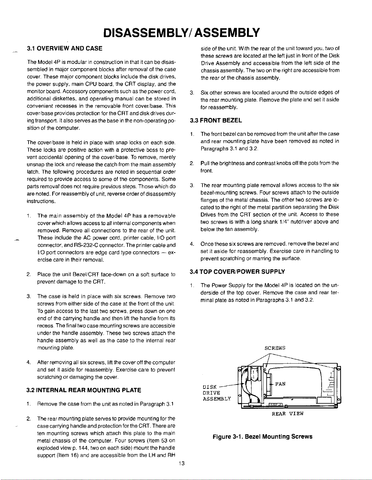
_-----rTI
top
cover.
DRIVE
ASSEMBLY
Figure 3-1. Bezel Mounting Screws
13
Remove
SCREWS
FAN
REAR
the
3.1
VIEW
case
and
and 3.2.
rear
ter-
2.
The
coverisattachedtothe
Remove these screws and then flip the cover to the right.
A
convenient
supply while workingonother modulesisto reattach the
cover/power
ing the assembly to rest above the disk drive assembly.
3.
The power supply is attached to the top cover with four
screws.
supply at the left and then four screws to remove the supply
completely from the unit.
arrangement
supplytothe
Remove
the
metal
for
chassis
connectors
chassis
storing
with
the
two
with
screws,
attachedtothe
cover/power
six
screws.
allow-
power
6.
Remove
CRT which attachitto the metal chassis. Carefully slide the
CRT out of the chassis through the front.
the
four
screws
and
washer
from
the
frontofthe
3.6 SWEEP BOARD
The CRT Sweep Boardisaccessible after the Ci;lT IS removed
from the unit.
with four screws.
and
the
reassembly.
Itismounted to the left side of the metal chassis
An
insulated plate is located between the PCB
metal chassis. Make
sure
this
plateisin
place
on
4.
When reassembling, ensure that the mylar insulatorispositioned between the power supply and the top cover to
provide
3.5 CATHODE
The CRT is mechanically attached to the metal chassis with
four
screws
1.
Remove
supply as notedinParagraphs 3.1, 3.2, 3.3, and 3.4. This
allows access to the connections
2.
Disconnect the deflection yoke cable from the CRT
board.
3.
Disconnect the connectoronthe rear of the CRT neck
which
The anode of the CRT may have a high voitage charge.
Before removing the high voltage (anode) iead, discharge
the CRT as follows to prevent a serious shock. Connect
one end of a wire to a known good ground and the other
end of the wire to the metal shaft of
screwdriver.
cup and touch it to the clip holding the high voltage lead.
4.
Disconnect the high voltage lead by inserting a grounded
screwdriver
press the clip and pull the wire tree.
5.
Disconnect fhe ground wire (fastenedatthe splice) to the
CRT neck connector PCB.
proper
insulation.
RAY
TUBE
which
are
accessible
the
case
rear
is
attached to a smallPCboard.
Insert
the
under
the
from
terminal
cover,
WARNING
screwdriver
cup.
Use
the
frontofthe
and
top
cover/power
on
the CRT.
an
insulated-handle
blade
under
the
the
screwdrivertocom-
unit.
PC
suction
3.7 MAIN LOGIC PCB
The main logic PCB is a large board nested inside a metal pan
at
the
bottomofthe
assembly, remove unit parts as notedinParagraphs
3.2.
Itisnot necessary to remove the power supply assembly,
or the CRT and associated PCB. Remove
rear of the unit. These include the Modem connector, I/O port
edge-card connector, printer edge-card connector, and floppy
disk edge-card connector.
1.
There
are
mounting pan which attach the pan to the metal chassis.
Remove
movedasa
2.
At
the front of the board, remove the four connectorsatthe
left front of the board. These include the reset, video,
power
connectors,
3.
Nine screws attach the main logic PCB to the metal pan.
The board is spaced away from the pan with raised bosses
stamped into the pan.
main
four
screws
these
screws
sUbassembly
metal
chassis.Togain
on each
and
the
board
from
the
andagrounding
accesstothis
all
connectorsatthe
side
of the metal PCB
and
pan
chassis.
wire.
3.1
and
canbere-
and
3.8 KEYBOARD ASSEMBLY
1.
The keyboard assembly is attached to the Main Logic PCB
with a connector located at the right rear of the board. The
PCB must be removed from the pan to allow this connector
to be removed. Therefore, disassembly procedures for the
main PCB must be followed.
2.
The keyboard assemblyisdisassembled by removing the
7 mounting screws from the underside of the assembly.
Oneofthese
should be takeninremoving this strip so thatitis
or punctured.
screwsisunderacork
non-skid
strip
not ripped
and
care
CAUTION:
If
the CRT is dropped,itmay implode.Toavoid this kind of
accident, carefully support the CRT when removing
the chassis. Do not handle the CRT by the neck
may cause the tube to break and cause
perso"al injury.
it
as
from
this
14
3.
Remove the top cover, lift the keyboard PCB from its positioning
bosses,
and
then
remove
the
connector.
keyboard
4.Ifthe cable assembly requires replacement, feed the connector through the opening
stall a tiewrap around the cable just before the insulation
sleeve.
This
servesasa
keyboard is reassembled. Ensure that this t',ewrap is in the
recess
between
bosses on the bottom of the case.
the
openinginthe
in
the keyboard base, then in-
strain
relief
for
the
cable
case
and
the
when
the
clamping
MOUNTING
SCREWS
DISK DRIVE
SU
BASSEMBLY
5.
Also ensure thatonreassembly the PCBisproperly positioned on the bosses of the base before attaching the top
cover.
Figure 3·2, Keyboard Cable Strain Relief
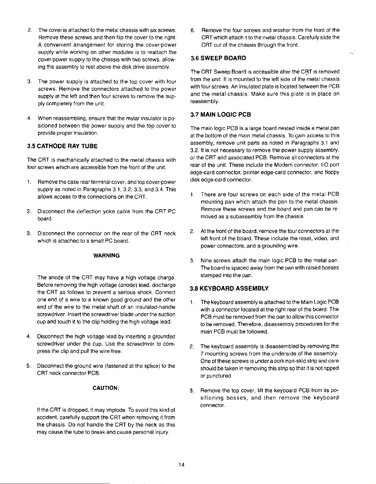
3,9
DISK DRIVE ASSEMBLY
The
disk drive assembly contains two floppy disk drives. it must
be
removed as asubassembly to the main metal chassis before
the
mounting
screws
for
the
drives
themselves
are
accessible.
•
o 0
BOTTOM PAN
o
Figure 3·3, Disk Drive Assembly
RH
Side View
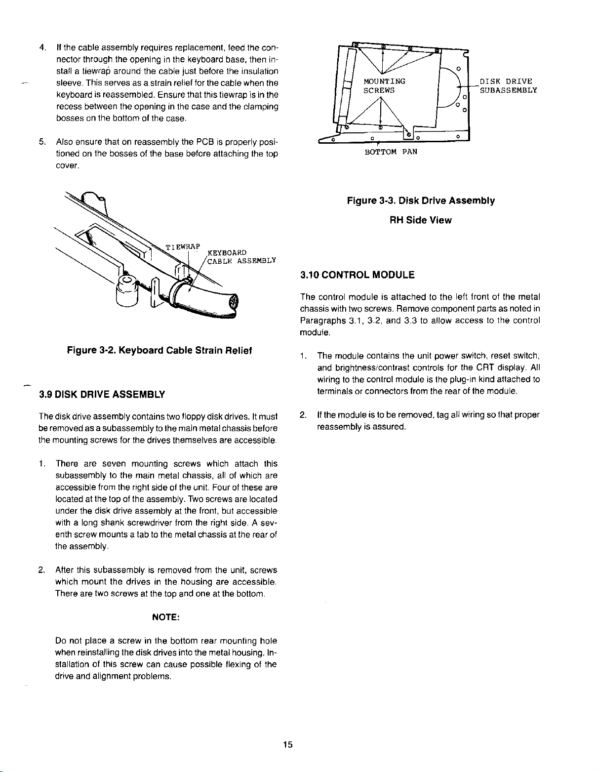
3,10 CONTROL MODULE
The control module is attached to the left front of the metal
chassis
Paragraphs 3.1, 3.2, and 3.3 to allow access to the control
module.
1.
2.Ifthe module is to be removed, tag all wiring so that proper
with
two
screws.
The module contains the unit power switch, reset switch,
and brightness/contrast controls for the CRT display. All
wiring to the control module is the plug-in kind attached to
terminalsorconnectors
Remove
from
component
the
rearofthe
partsasnoted
module.
reassemblyisassured.
in
1.
There are seven mounting screws
subassembly to the main metal chassis, all of which are
accessible from the right side of the unit. Four of these are
located at the top of the assembly.
under the disk drive assembly at the front, but accessible
with a long shank screwdriver from the right side. A
enth screw mounts a tab to the metal chassis at the rear of
the assembly.
2.
After this subassembly is removed from the unit, screws
which
mount the drivesinthe housing are accessible.
There are two screws at the top and one at the bottom.
NOTE:
Do not place a screw in the bottom rear mounting hole
when reinstalling the disk drives into the metai housing. installation of this screw can cause possible flexing of the
drive and alignment problems.
which
Two
screws are located
attach
this
sev-
15
0
o
@
@
II
I !
Irr
0
FRONT REAR
BRIGHTNESS
CONTRAST
POWER
ON/OFF
RESE'r
BRN
BRN
.....
-I.L~
BLU
t-~~~-'9I
Ii-=:-':~~-e
~BLK
o
--ft--,Y
II
B
LU
YlEL.'1
CRT
BOARD
Figure 3-4. Control Module
16
SECTION IV
MAINTENANCE/TROUBLESHOOTING
17

4.1
INTRODUCTION
MAINTENANCE/TROUBLESHOOTING
This sectionisa general guide for use by service personnel.
contains the Maintenance and Troubleshooting procedures
necessary to help isolate the problem area to a faulty board or
sUbsystem. After board or subsystem has been identified, refer
to
specific
section
for
more
detailed
troubleshooting
information.
Refer to the schematics and the theory of operation during
maintenance and troubleshooting for specific checkpoints and
testing.
4.2 MAINTENANCE
The oniy part of the Model 4P that requires maintenanceisthe
two Floppy Disk Drives. Periodical cleaning of the Read/Write
Heads
are
recommendedtoassure
other maintenanceoralignments required, refer to Section 5.3
Mini-Disk Drives Maintenance Checks and Adjustments.
error-free
operation.
For
4.3 TROUBLESHOOTING
Please be sure that the powercord is properly connected to
power before starting troubleshooting.
1.
Turn
Model 4P
light indicator
2.
RecheckACpower and power cord.Ifokay go to3,if bad
"ON"
by toggling power switch.Ifpower
is
on then go to4,if not, go to
2.
AC
replaceorrepair.
3.
Checkpower switch and bulb.Ifokay go to 1,ifbad repiace
power switch or bulb.
4.
Wait a few seconds for CRT to warm
and contrast at the front of consoie.
on go to
5.
Check p'Jwer switch.Ifokay go to6,if bad replace.
9,
if not go to
5.
up.
Adjust brightness
If
video display comes
all
It
10.
Does message "Close the Floppy Drive Door And Try
Again" appear?
11. Does message "The Floppy Disk Drive
appear?
12.
Does message "CRC Error,
Disk" appear?
13.
Does message "Seek Error, Try Again Or Use Another
Disk" appear?
14.
Does any other message appear?Ifyes then refer to Appendix B Startup Error Messages in Introduction to Your
Disk System TRS-80 Model 4P, if not then go to
15.
Insert Write Protected Diskette with TRSDOS
into Drive
4P boot up to TRSDOS Logo and prompt for date?
then go to 18, if not then go to 16.
16. Does message "The Floppy Disk Drive
appear?
Try
17.
18.
19. This indicates a hardware failure of Floppy Disk intertace
to boot again or use another diskette.Ifokay go to 18.
if still same message then go to 19.
pears, go to
This indicates that the problem area existsonthe Main
Logic CPU Board. Refer to Section 5.1.17
Board TroUbleshooting for more detailed troubleshooting
procedures.
or Floppy Disk Drive. Refer to Section 5.1.17 or 5.2.17
CPU
Board Troubleshooting or Section 5.3 Mini-Disk Drive
Maintenance Checks or Adjustments.
If
yes, go to 17, if not go to 11.
Is
If
yes then go to 19, if not go to 12.
Try
Again Or Use Another
If
yes then go to 19,ifnot go to 13.
If
yes then go to 19, if not go to 14.
0,
close door and toggle RESET Switch. Does
Is
If
yes then go to 17, if not then go to 10.
If
anothermessage ap-
9.
Not Available"
5.
6.1.1
or later
If
yes
Not Ready" still
or
5.2.17 CPU
6.
Check forACpower at input to power supply.Ifokay go to
7,
if bad replaceorrepairACwiring harness.
7.
Check power supply for correct output voltages. (Refer to
Power Supply Section 5.4.)
Power Supply Troubleshooting 5.3.4.
8.
Check for video and sync signais from Main Logic Board
J9. (Refer to CPU Board Section and Schematic.)Ifokay
refer to CRT Display Adjustment Section 5.5.2, if bad refer
to CPU Board Troubleshooting Section 5.1.17 or 5.2.17.
9.
Does message "The Floppy Disk DriveIsNot Ready" appear?
If
yes go to 15, if not go to 10.
If
okay go to8,if bad refer to
at
19
SECTION V
4P THEORY OF OPERATION
21

4P THEORY OF OPERATION
5.1
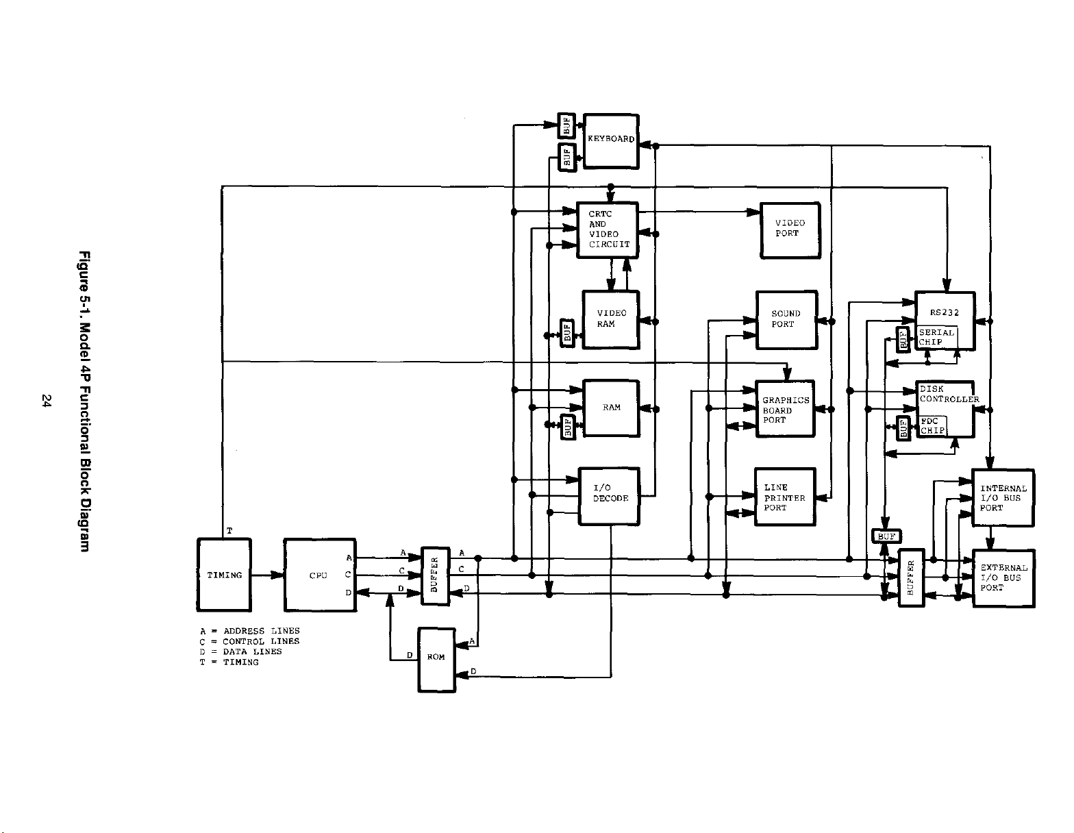
CPU THEORY OF OPERATION
5.1.1
Introduction
Containedinthe following paragraphsisa description of the
component parts of the Model4P CPU.
ical
operational
locatedonthe Main CPU board inside the case housing. Refer
to
Section 3 for disassembly/assembly procedures.
functionsofthe
5.1.2 Reset Circuit
Itisdivided into the log-
computer.
All
components
are
(pin 9 of U126).IfFASTisa logic low, the 20.2752 MHzisdivided by 10 which generates a 2.2752 MHz signal
logic high, the 20.2752 MHz
4.05504 MHz signal. The CPU clock (PCLK)
active
pull-up
circuit
which
rise and fall times required by the Z80A. U126. the 16R6A
generates
low the PCLK output to short cycle or generate a low or high
pulse
RefertoSystem Timing Fig. 5-2.
under
all
symmetrical
110
nanoseconds
is
divided by 5 which generates a
generates a
output
signals
which
ful15-volt
and
the
ZaOA
If
is
fed through
swing
also
does
also
FASTisa
an
with
fast
PAL.
not
al-
requires.
The Model 4P reset circuit provides the neccessary reset
pulsestoall
and C218 provide a time constant which holds the input of
low during power-up. This allows power to be stable to
cuits before the
C218 charges to a logic high, the output of
input of a retriggerable one-shot mullivibrator
a pulse with
reset switch is pressed on the front panel, this discharges C218
and
holds the input of
release of the switch, C218 again charges up, triggering
andU1to
circuits
during
powerupand
RESEr
an
approximate width of70microsecs. When the
reset
the
and RESET signals are applied. When
U121
low until the switch is released.
microcomputer.
reset
operations.
U121
(Ul).Uloutputs
R25
U121
all
cir-
triggers the
On
U121
5.1.3 CPU
The central processing unit (CPU) of the Model 4P microcomputer
is
a Z80A microprocessor. The Z80A is capaqle of run-
ning in either 2 MHz
functionsofthe
(AO-A
15), data lines
/RO,
/WR, /MREQ, and /RFSH). The address lines
are
buffered to other ICs through two 74LS244s (U68 and U26)
which are enabled all the time with their enables pulled to GNO.
The control lines are buffered to other ICs through a 74F04
(U86). The data lines
tionaI74LS245 (U71) which
rection
is
controlled by BUSOIW.
or
4 MHz mode. The CPU controls all
microcomputer
(00-07),
(00-07)
is
through
and control lines
are buffered through a bi-direcenabled by BUSEW and the di-
useofits
address
(lMl,
lines
/IOREQ,
(AO-A
15)
5.1.4 System Timing
The
main
timing
referenceofthe
ception of the FOC circuit, comes from a 20.2752 MHz Crystal
Oscillator (Y1). This reference
ating all necessary timing for the CPU, video circuit, and
232-C circuit. The output of the crystal oscillatorisfiltered by a
ferrifte bead (FB5), 470 ohm resistor (R46), and a
pacitor (C242). After being filtered,
PAL
(Programmable Array Logic), whereitis divided by 2 to
generate a 10.1376 MHz signal (10M) for the
play. U126 divides the 20.2752 MHz
MHz signal (RS232CLK) for the baud rate generator
232-C circuit. The
can
be
either 2 or 4 MHz dependingonthe state of
CPU
clockisalso generated by U126 which
microcomputer,
is
divided and used for gener-
itisfed into U126, a 16R6A
by
4 to generate a 5.0688
64X16
with
the
68pfca-
video dis-
in
the RS-
FAST
ex-
RS-
input
5.1.4.1 Video Timing
The video timing is controlled by a 1
bit synchronous counter U128 (74LS161). These two ICs generate all the necessary timing signals for the four video modes:
64x16,
nals
clock, the 10.1376 MHz signal (10M),isgeneratedbyU126 and
is
ence clock
a Phase Locked Loop (PLL) circuit and
and 40 x24modes. The PLL circuit consists of U147 (74LS93),
U148 (NE564 PLL), and U149 (74LS90). The original 20.2752
MHz clock
1.2672 MHz signal. The output of U147 is reduced
by
coupledtothe reference input of U148 by C227.
The PLL (NE564)isadjusted to oscillate at 12.672 MHz by the
luning capacitor C231. This 12.672 MHz clock
by
whioh is fed to a second input of U148. The two 1.2672 MHz
signals
12.672 MHz output soitis
clock.
MOOSEL and
video mode.
U127 and MOOSEL controls the single or double character
width mode. Refer to the following chart for selecting each
video
32 x 16,80x 24, and 40 x 24.
are
required
used by the64x 16 and32x 16 modes. The second refer-
is
the voltage divider network R27 and R28 and the output
10 through U149 to generate a second 1.2672 MHz signal
are
mode.
8064'
for
the
four
a 12.672 MHz (12M) signal whichisgenerated by
is
divided by16through U147 which generates a
compared
8064'
internallytothe
synchronized with the 20.2752 MHz
8064'
signals are used to select the desired
controls which reference clockisused by
MOOSEL
o
o
1
1
'This
is the state to be wriften to latch U89. Signalisinverted
before being input to U127.
OL8
PAL
(U127) and a four-
Two
reference clock sig-
video modes. One reference
is
usedbythe 80 x
in
is
then divided
PLL
whereitcorrects
Video Mode
o
1
o
1
64 x 16
32 x 16
80
x24
40
x 24
amplitude
the
24
is
23
...
'"
cEo
"
c:
~
CD
'!'
-
;;:
0
Co
!2.
...
"tI
c:
"
:::l
"
-
0"
:::l
!!!.
III
0"
,..
"
9-
..
IC
~
..
3
T
TIMING
-
A = ADDRESS
C::CONTROL
D::DATA
T
'"
TIMING
LINES
LINES
LINES
CPU
~
...
-
*'
~
CRTC
AND
VIDEO
CIRCUIT
~
VIDEO
PORT
f
RS232
SERIAL
~
CHIP
• t
DISK
:::TROLLE~
a:
CHIP
~
..
"t
INTERNAL
I/a
BUS
~
-A
~
~
~
~
~
~
-
EXTERNAL
*
I/O
BUS
PORT
~
VIDEO
RAM
..
-
SOUND
PORT
•
rti
t
..
GRAPHICS
BOARD
PORT
I-
~
RAM
..
Kt
I/O
DECODE
f-
..--
r--
A
C
0
C
0
........E..
~
~
~
~
~
~
.....
r--
ROM
A
C
0
~
0
LINE
•
PRINTER
PORT PORT
...
i-
Qm
2jJ MC,
<0126
<0126
(U126
<0126
(U
"T1
.co
c:
~
U1
~
1Il
"
~
'"
co
-
3
-i
3°
oj'
lC
126
<012~·~~N
PSET
(U126
PCLK
<0126
2jJI
PIN
2jJM
PIN
1jJM
PIN
1jJS
PIN
5S
PIN
(FAST)
PIN
(FAST)
PIN
1,2)
12)
16)
J I 1 I 1 I 1 I I I , L
15)J
14)
I I 1 I I
13>J
J I
IS)
..Jr--------...,
19)
I I I I I I I I
I I I
1~
----'1
....11
I I
I I
I~---
PSET
<0126
PCLK
(U126
RS232CLK
U126
(FAST)
PIN
(FAST)
PIN
PIN
lS)J
19)
-l
J-----....,
17)
I
I
I
.......JI
~
I 1 _
Ir----
I~---
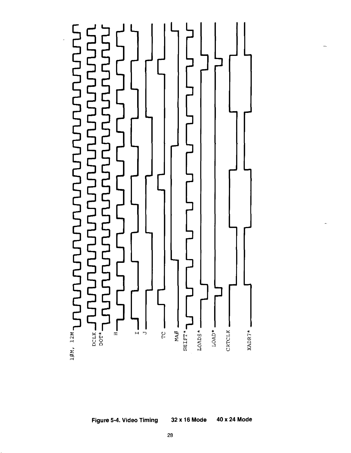
DCLK, the reference clock selected,isoutput from U127. DCLK
is
fed
back
info
U127
tor
internal
fedtothe clock inpui of U128 (74LS161). U128 is configured to
preload with a count of g each time
generates a signal output of TC (128 pin 15) that occurs at the
every character time of video output.
start of
erate LOADS' (Load Shift Register). QA and QC of U128 are
used to generate
proper timing for the four video modes. QA, QB, and
are referred to as
reference
ing, Figs. 5-3 and 5-4 for timing reference.
timingsofHires
SHIFr,
H,I,and J are fed to the Graphics Port J7 for
graphics
riming
reference
it
reaches a count ofO.This
XADR7", CRTCLK and LOAD' for
video.
RefertoVideo
andisalso
TCisusedtogen-
QC
which
Tim-
5.1.5 Address Decode
The Address Decode section will be divided into two subsections: Memory Map decoding and Port Map decoding.
The Model 4P Boot ROM contains all the code necessary to
initialize hardware, detect options selecled from
read a sector from a hard disk or floppy, and load a copy of the
Model III ROM-Image (as mentioned) into the lower 14K of
RAM.
The
firmwareisdivided
Hardware
Keyboard Scanner
Control
Floppy and Hard Disk
Disk Directory Searcher
File Loader
Error Handler and Displayer
RS-232 Boot
Diagnostic Package
into
Initialization
the
Driver
following
the keyboard.
routines:
5.1.5.1 Memory Map Decoding
Memory Map Decoding is accomplished by a 16L8
Four
memory
with the Model
PAL
(U110)isusedinconjunction with U109 for the memory
map control which also controls page mapping of the 32K RAM
pages. Refer to Memory Maps below.
map
modes
are
available
III
and Model 4 microcomputers. A second 16L8
which
PAL
are
compatible
(U1
09).
5.1.5.2 Port Map Decoding
Port Map Decodingisaccomplished by three 74LS138s (U87,
U88,
and U107). These ICs decode the low order address
A7)
from the CPU and decode the port being selected. The
signal from U108 enables U87 which allows the CPU to read
our
from a selected port and the
ables U88 which allows the CPU to write to the selected port.
U1
07 only decodes the address and the IN" and
are ANDed with the
gener~ted
signal, also from U108, en-
our
signals.
(AO-
IN'
signals
5.1.6 ROM
The Model 4P contains only a 4K x 8 Boot ROM (U70). This
ROMisused only to boot up a Disk Operating System into the
RAM
memory.IfModel III operation or DOS is required, then
RAM
the
age of the Model
tem program called MODEL A/III is supplied with the Madej 4P
to
power-up, the Boot ROMisselected and mapped into location
OOOO-OFFFH.
Boot ROM must be mapped out by OUTing to port 9CH with
set orbyselecting Memory Map modes 2 or3.In
RAMiswrite enabled for the
mapped where Boot ROM
ecuting out
from location 0000-37FFH must be loaded with an im-
III
or 4 ROM code and then executed. A sys-
provide the ROM image for proper Model
If the Boot ROM is not required after boot
fuII14K. This allows the RAM area
is
located to be writtentowhile ex-
of
the Boot ROM. Refer to Memory Maps.
III
operation. On
up,
the
DO
Mode 1 the
Theory of Operation
This
section
ROM. Normally, the ROM is not addressable by normal use.
However,
fixed calling locations and these may be used by operating systems that are booting.
On
a power-up or RESET condition, the Z80's program counter
is set to address 0
ory map of the systemisset to ModeO.(See Memory Map for
details.) This will cause the Z80 to fetch instructions trom the
boot ROM.
The Initialization section of the Boot ROM now performs these
describes
there
are
several
and
the
operationofvarious
the
routines
boot
that
ROM
routinesinthe
are
available
through
issWitched-in. The mem-
functions:
1.
Disables maskable and non-maskable interrupts
2.
Interrupt mode 1isselected
3.
Programs the CRT Controller
4.
Initializes the boot ROM control areasinRAM.
5.
Sets up a stack pointer
6.
Issues a Force Interrupt to the Floppy Disk Controller
to
abort
any
current
7.
Sets the system clock to 4mhz
8.
Sets the screen to 64 x 16
9,
Disables reverse video and the alternate character
sets
10.
Tests for < . > key being
11.
Clears all 2K of video memory
* This
is
a special test.Ifthe
is
control
ROM. All
Scanner.
transferredtothe diagnostic packageinthe
other
keys
activity
<'
are
scanned
pressed'
:>
is
being pressed, then
via
the
Keyboard
26

:>:
N
.-i
lSt
.-i
:>:
:<:
-<
U
Q
"
E-<
0
Q
"
"
r..
""'
H
p::
til
0
til
Q
<t:
-<
p::
,.,
H
""'
~
lSt
U
"
~
0
-<
~
-<
U
E-<
cr;
u
"
r-
cr;
~
:><
Figure 5·3. Video Timing 64 x16Mode
27
80x24
Mode
:E
N H
H
:E
H
""
r,
'"
uO
Q Q
~
Eo<
'"
H
Figure 5-4. Video Timing
U
Eo<
<l:
""
:E
32x16
28
~
Eo<
0<
H
Ul H
'"
Mode
~
~
Q
(JJ
Q
<l:
0
<l:
0
H
40x
H
'"
U
Eo<
~
U
24 Mode
~
r-
~
Q
<l:
><
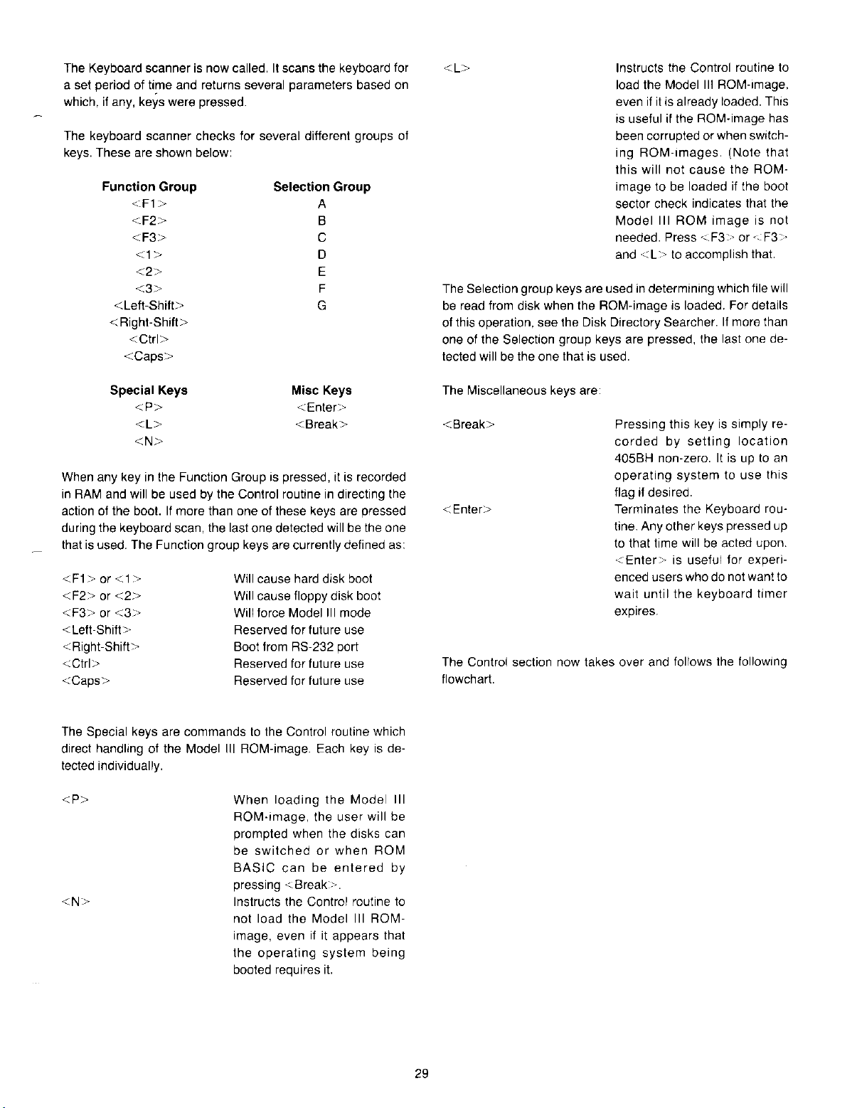
The Keyboard scannerisnow called. It scans the keyboard for
a set period of
which,
if
The keyboard scanner checks for several different groups of
keys. These are shown below:
Function
ti:ne and returns several parameters based on
any, keys were pressed.
Group
<F1>
Selection
A
<F2>
<F3>
<1>
C
D
<2>
<3>
<Left-Shift>
<Right-Shift>
G
Group
B
E
F
<Gtrl>
<Caps>
<L>
The Selection group keys are used in determining which file will
be
read from disk when the ROM-image is loaded. For details
of this operation, see the Disk Directory Searcher. If more than
one of the Selection group keys are pressed, the last one detected will
be
the one that is used.
Instructs the Control routine to
load the Model
even if it is already loaded.
IS
useful if the ROM-image has
been corrupted or when switching
ROM-Images.
this
will
image to be loaded if the boot
sector check indicates that the
Model
needed. Press
and
III
<L>
III
ROM-Image,
(Note that
not
cause
the ROM-
ROM
imageisnot
<F3>or<F3'
to accomplish that.
ThiS
Special
When any key
in
RAM and will be used by the Control routineindirecting the
action of the boot.
during the keyboard scan, the last one detected will be the one
that
is
used. The Function group keys are currently defined as:
<F1>or<1>
<F2>or<2>
<F3>or<3>
<Left-Shift>
<Right-Shift>
<Gtrl>
<Caps>
The Special keys are commands
direct handling of the Model
tected individually.
<p>
<N>
Keys
<p>
<L>
<N>
in
the Function Group is pressed, itisrecorded
If
more than one of these keys are pressed
Will cause hard disk boot
Will cause floppy disk boot
Will force Model
Reserved for future use
Boot from RS-232 port
Reserved for future use
Reserved for future use
III
ROM-image. Each keyisde-
When
ROM-image,
prompted when the disks can
be
BASIC
pressing
Instructs the Control routine to
not
image, even
the
booted requires it.
Misc
Keys
<Enter>
<Break>
III
mode
to
the Control routine which
loading
switched
can
load
operating
the
the
user
or
when
be
entered
<Break--,
the
Model III ROM-
if
it appears that
system
Model
will be
ROM
being
III
by
The Miscellaneous keys are:
is
<Break>
<Enter>
The Control section now takes over and follows the following
flowchart.
Pressing this key
corded
405BH non-zero.Itis
operating
flag If desired.
Terminates the Keyboard rou·
tine. Any other keys pressed up
to that time will
<Enter>
enced users who do not want to
wait
expires.
by
setting
systemtouse
is useful for experi-
until
the
simply re-
location
up to an
be
acted upon.
keyboard
this
timer
29
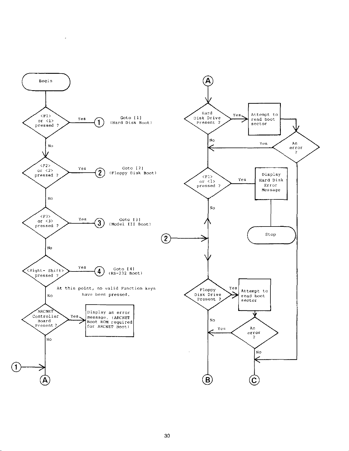
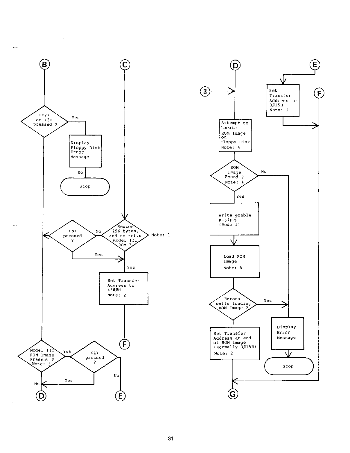
Begin
A
1
A
30
B
B
c
D
<F2>
or
<2>
pressed?
Yes
Display
Floppy
Error
Message
<N>
pressed
?
No
Stop
Disk
No
Yes
256
and
Sector
no
Model
ROM
bytes,
ref.s
?
Yes
III
Note:
Set
Transfer
Address
3~l5H
Note:
Attempt
locate
ROM
on
Floppy
Note:
Found
Note:
Write-enable
~-37FFH
(Mode
1
Load
Image
Note:
Image
ROM
Image
to
Disk
4
No
?
4
Yes
1)
ROM
5
to
2
F
No
D
Set
Transfer
<L>
pressed
?
Address
43~~H
Note:
2
®
to
Errors
while
ROM
Set
Transfer
Address
of
ROM
(Normally
Note:
loading
Image
at
Image
2
?
end
3~15H)
Yes
Display
Error
Message
Stop
No
~
Yes
":"::':""
__
---.J
E
G
31
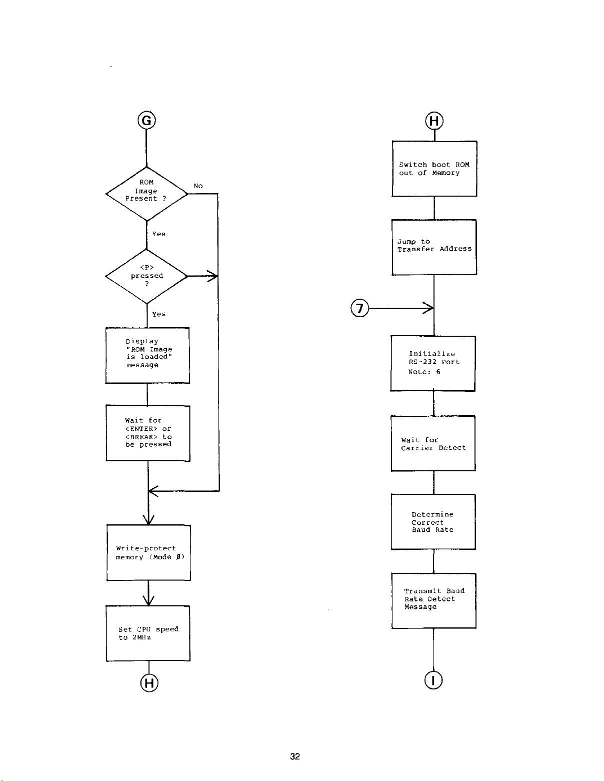
G
ROM
Image
Present
~
boot
Switch
out
of
No
?
ROM
Memory
<p>
pressed
?
Display
II
ROM
Image
is
loaded
message
Waitfor
<ENTER>
<BREAK>
be
pressed
Yes
Jump
to
.....
,
tiali
6
foe
Determine
Correct
Baud
Rate
Address
ze
Port
Detect
Transfer
7
II
or
to
Ini
RS-232
Note:
Wait
Carrier
Write-protect
memory
Set
to
CPU
2MHz
(Mode
H
speed
0)
Transmit
Rate
Message
Detect
Baud
I
32
Wait
Sync
(FFH)
for
Byte
Packages that do not reference the Model III ROMinthe
boot sector can still cause the Model
loaded by coding a
It
does not have to be executable.Atthe same time, Model
4 packages
CDxxOO
must
take care that thereisno
somewhereinthe boot sector.
III ROM image to be
sequence
bytesinthe boot sector that could be mis-interpreted to be
a reference to the Boot ROM. An example of this would be
sequence
06CDOEOO,
which is a LD B,OCDH and a LD
C,O.Ifthe boot sector cannot be changed, then the user
must press the
to inform the ROM that the disk contains a Model
age which needs the Model
<F3>
key each time the systemisstarted
III
ROM-image.
III
pack-
of
Load
program
from
RS-232
Notes:
An
error
Transfer
control
to
address
recei
?
ved
Yes
Display
transmit
and
error
(1)Ifthe boot sector was not 256 bytesinlength, thenitis
sumed to be a Model III package, and the ROM-image will
be needed. If the sector is 256 bytes
sector
is
scanned for the sequence
the first byte of a
ZBO
unconditional subroutine call. The
in
length, then the
CDxxOOH.
TheCDis
next byte can have any value. The third byte is tested
against a zero. What this check does is test for any references
to
the first 256 bytes of memory. All Radio Shack
Model
III
operating systems, and many other packages all
reference the ROM at some point during the boot sector.
Most boot sectors will display a message
not be loaded.Tosave
Model
III
ROM calls to display the message. Several
space, these routines use the
if
the system can-
calls have their entry pointsinthe first 256 bytes of memory, and these references are detected by the boot ROM.
as-
ROM
(2)Ifyou are loading a Model 4 operating system, then the
boot ROM will always transfer control to the first byte of the
boot sector, which is
III
operating system or about to use Model
at
4300H.Ifyou are loading a Model
III
ROM BASIC,
then the transfer address is 3015H. This is the address of
ajump
vectorinthe
"C"
ROM of the Model III ROM image,
and this will cause the system to behave exactly like a
Model III.
If
the ROM-image file that is loaded has a differ-
ent transfer address, then that address will be used when
loading
is
complete.Ifthe imageisalready present,itwill
use 3015H.
(3)
Two
different tests are done to insure that the Model III
ROM image
is
present. The first test is to check ever third
location starting at 3000H for a C3H. This is done for 1010-
cations.Ifanyofthese locations does not contain a C3H,
then the ROM image is considered to be
The next test is to check two bytes at location
these addresses contain
E9E1H,then the ROM image is
"not
present".
OOOBH.
considered to be "present".
(4)
See Disk Director Searcher for more information.
(5)
See File Loader for more information.
(6)
The RS-232 loaderisdescribed under RS-232 Boot.
Disk Directory
When the Model
from the floppy
Searcher
III
ROM image
in
drive
O.
isto
be loaded,itis
always read
Before the operation begins, some checks are made. First, the
boot sector is read in from the
checked to make sure
itiseither a
floppy
and the first byte is
OOH
or a FEH.Ifthe byte
contains some other value, no attempt will be made to read the
ROM
image from that disk. The location of the directory cylinder
is
then taken from the boot sector and the type of disk is deter-
mined. This
is
done by examining the Data Address Mark that
If
33
was picked up by the Floppy Disk Controller (FDC) during the
1,
read of the sector. II the DAM equals
1.x style disk. Ifthe DAM equals
TRSDOS 6 style disk. This
0,
is
important since TRSDOS 1.x
the diskisa TRSDOS
then the diskisa LDOS 5.1/
disks number sectors starting with 1 and LDOS style disks
number sectors starting with
Once
the
disk
type
has
if
the diskisa LDOS style disk. This test reads the Granule Al-
O.
been
determined,anextra
t8St
is
made
location Table (GAT)todetermine if the disk is single sided or
double sided.
Floppy
The
disk
and
drivers
Hard
Disk Driver
are
entered
via
RSTBHand
will
readasector
anywhere on a floppy disk and anywhere on head 1 (top-head'
in
a hard disk drive. Either 256 or 512 byte sectors are readable
by
these
size.
and the
routines
The'11ard
WD1010controllers. The floppy disk driveriswritten for
and
they
make
the
determinationofthe
sector
disk driver is compatible with both'the WD1000
the WD1793 controller.
Loader
Serial
The
directoryisthen
read
one
recordata
time
andacompare
is made againsf the pattern 'MODEL% ' for the filename and
'III'
for
the extension. The
'%'
means that any character
will
match this position. II the user pressed one of the selection
keys (A-G) during the keyboard scan, then that character is
substituted
piace of the
'%'
character. For example,ifyou
in
pressed 'D', then the search would be for the file 'MODELD "
with the extension
it
finds the entry or it reaches the end of the directory.
'Ill'. The searching algorithm searches until
Once the entry has been found, the extent information for that
fileiscopied
File
Loader
intoacontrol
block
for
later
use.
The file loaderisactually two modules - the actual loader and
a set of routines to fetch bytes from the file on disk. The loader
is
invoked via a RST 28H. The byte fetcher is called by the
loaderusing RST 20H. Since restart vectors can be re-directed,
the same loader is used by the RS-232 boot. The difference
that the RST 20Hisredirected to point to the RS-232 data re-
ceiving
routine.
The loader
reads
standard
loader
records
and
acts upon two types:
01
Data Load
1 byte with length of block, including address
1 word with address to load the data
n bytes of data, where n
+2 equals the length specified
02 Transfer Address
1 byte with the value of 02
1
word
with
the
addresstostart
execution
at.
Any other loader code is treated as a comment block andisignored. Once an 02 record has been found, the loader stops
if
reading, even
thereisadditional data, sobesure to place the
02 recordatthe end of the file.
Invoking
the
serial
loaderissimilartoforcingaboot
disk or floppy.Inthis case the right shift key must be pressed
some
time
during
the
first
three
gram
does
not
careifthe
venienttoconnect
seconds
keyispressed
pins8and10of
the
after
forever,
keyboard
a shorting plug for bench testing of boards. This assumes that
the object program being loaded does not care about the key
closure.
Upon entry, the program first asserts DTR (J4
4)
(J4 pin
of
true. Next, "Not Ready"isprinted on the topmost line
the video display. Modem status line CD (J4 pin8)is
sampled. The program loops until it finds CD asserted true.
that time the message "Ready"isdisplayed. Then the program
sets
about
To
determine
determining
the
the
baud
rate
from
the
baud rate, the program compares data
ceived by the UART to a test byte equal to '55' hex. The receive
is
first set to 19200baud.Iften bytes are received which are not
is
equal
is
repeated
to
the test byte, the baud rateisreduced. This sequence
untilavalid
test
byteisreceived.Iften
at50baud, the entire process begins againat19200 baud.Ifa
valid
test
rive
before
rate.Ifat
byteisreceived,
concluding
this
timeanimproper
the
program
thatithas
byteisreceivedora
waits
determined
for
ror (overrun, framing, or parity)isintercepted, the task begins
again at 19200 baud.
In
order to get to this point, the host or the modem must assert
CD true. The host must transmit a sequence of test bytes equal
to
'55' hex with 8 data bits, odd parity, and 1 or 2 stop bits. The
test bytes should be separated by approximately
avoid
overrun
errors.
When the program has determined the baud rate, the message:
"Found Baud Rate x"
from
reset.
The
makingitcon-
connector
pin
20) and RTS
host
computer.
failures
ten
moretoar-
the
correct
receiver
0.1
second to
hard
at
pro-
with
then
At
re~
occur
baud
er-
is
displayedonthe
meaning:
A
~
B
~
C~110
~
D
34
50 baud
75
134.5
screen, where
~
150
E
~
300
F
~
600
G
~
1200
H
I
~
J
K
L
"x"isa
1800
~
2000
~
2400
~
3600
letter
fromAto
~
M
~
N
o
~
P
~
19200
P,
4800
7200
9600
 Loading...