

Page 1

TRC-447
40-CHANNEL MOBILE CB
WITH WX ALERT
Catalog Number: 21-1576
21-1576
CONTENTS
Page
Specifications ................................................................................................................................................. 2
Block Diagram ................................................................................................................................................ 5
Alignment and Adjustment ............................................................................................................................. 6
Troubleshooting ........................................................................................................................................... 10
Wiring Diagram ............................................................................................................................................ 16
Printed Circuit Boards .................................................................................................................................. 17
Exploded View and Disassembly Instructions.............................................................................................. 20
Mechanical Parts List ................................................................................................................................... 23
Electrical Parts List ...................................................................................................................................... 24
Semiconductor Lead Identification ............................................................................................................... 43
IC Internal Diagrams .................................................................................................................................... 44
IC and Transistor Voltage Chart................................................................................................................... 46
Schematic Diagrams .................................................................................................................................... 50
2004 RadioShack Corporation.
RadioShack is a registered trademark of RadioShack Corporation.
All Rights Reserved.
Page 2

SPECIFICATIONS
GENERAL
Channels: 40 (CB Transceiver)
7 (Digital Weather Alert Radio)
Frequency range: 26.965 MHz to 27.405 MHz (CB)
162.400 MHz to 162.550 MHz (WX)
Frequency control: PLL controlled synthesizer
Microphone: Electret condenser type microphone with channel up/down switch
Antenna impedance: 50-ohm
Controls: Volume control with Power on/off Switch
Squelch control for CB
SWR Cal Control for CB
RF gain control for CB
Mic Gain Control for CB and PA
Switches: CH9-NOR-CH19 Lever Switch for CB
S/RF-SWR-CAL Lever Switch for CB
CB-WX-PA Lever Switch
NB-OFF-MON Lever Switch
DUAL-OFF Lever Switch for CB
Channel Rotary Switch for CB and WX
Indicators: Channel number (LED: Green color)
TX/RX (LED:TX-Red/RX-Green Color)
WX/ALERT (LED:Red Color)
Antenna connector: M Type (SO 239)
Jacks: Mic 6 pin Screw Type
EXT. SP 3.5 dia.
PA. SP 3.5 dia.
Dimensions (HWD): 55mm × 185 mm × 225 mm
Weight: 1.4 kg
Power supply: 12 V DC rated (13.8 V DC)
Operating temperature range: −30 °C to +50 °C (FCC Stability)
Storage temperature range: −30 °C to +60 °C (Without damage)
Accessories: Microphone
Microphone hanger with screws
Mounting bracket with screws
DC Power Cord with Fuse
Owner's manual
Measuring Conditions
Power supply voltage: 13.8 V DC
Temperature and humidity: 25 ±5 °C, 50 to 70%
Output load for transmitter: 50 ohm Resistive
Input signal source: 50 ohm SSG
Test input signal: 1 kHz, 30% Modulation (CB)
1 kHz, ±3 kHz Deviation (WX)
FSK, ±4.5 kHz Deviation (Digital WX Alert)
Output Load for Receiver: 8 ohm Resistive
Reference Audio Output Power: 0.5 W
Measuring Channel: CH 20 (CB)
CH 5 (WX)
Each Function Knob Condition.
Volume: Fully clockwise (FCW)
Squelch: Unsquelched
RF gain: Fully clockwise (FCW)
Mic Gain: Fully clockwise (FCW)
CH9-NOR-CH19: NOR
NB-OFF-MON: OFF
DUAL-OFF: OFF
✽ FCC type acceptance specification for PART 15 and 95.
✽ Frequency tolerance and specification: ±0.005% from −30 °C to +50 °C
— 2 —
Page 3

CB TRANSMITTER PORTION
Item Unit Nominal Limit
Frequency tolerance 25 °C 13.8 V Hz ±200 ±1300
RF Power output W − 4
AMC range 50% to 100% modulation dB 45 35
Modulation frequency response Lower frequency 450 Hz dB −3 −10
Upper frequency 2500 Hz dB −3 −10
Microphone sensitivity 1 kHz, 50% Mod. mV 4 10
Modulation distortion 1 kHz, 80% Mod. % 3 8
Battery drain at No modulation mA 900 1300
at 80% modulation mA 1300 1900
RF Power output at 12 V W 2.7 2.2
Modulation attack time mSec 100 300
Modulation release time mSec 800 500
CB RECEIVER PORTION
Maximum sensitivity µV 0.5 1
Sensitivity for 10 dB S/N µV 0.5 1
AGC Figure of merit 50 mV for 10 dB change in audio output dB 90 75
Threshould squelch sensitivity µV 0.5 1
Tight squelch sensitivity µV 1000 250 ~ 4000
Adjacent channel selectivity at ±10 kHz dB 50 40
Spurious rejection ratio dB 45 30
Image rejection ratio (−910 kHz) dB 65 55
IF rejection ratio 10.695 MHz dB 60 50
455 kHz dB 90 60
Audio output power Maximum 8-ohm W 5.5 4.0
10% Distortion 8-ohm W 4.0 3.5
Audio frequency response Lower frequency 450 Hz dB −3-10
Upper frequency 2500 Hz dB −3-10
THD at 500 mW audio output 1 mV 30% input % 3 5
Signal to noise ratio at 1mV dB 40 35
Oscillator on voltage V 5 11
Battery drain at No signal mA 300 350
at Maximum AF output mA 1000 1500
RF gain control range at 1 µV reference dB 30 20
S-meter sensitivity at S-9 µV 100 50 ~ 200
WEATHER RADIO SECTION
Sensitivity at 2.0 µV Input dB SINAD 27 15
THD at 500 mW audio output
Input 1 mV ±3 kHz deviation % 3 7
Signal to noise ratio at 1 mV dB 45 35
Audio output power Maximum 8-ohm W 5.5 4
10% Distortion 8-ohm W 4 3.5
Digital weather alert sensitivity
Input SAME data (FSK) ±4.5 kHz dev. µV 0.5 1.0
— 3 —
Page 4
CHANNEL FREQUENCY OF PLL SYNTHESIZER
CB BAND
Antenna
CH
10 27.075 27.075 16.380
11 27.085 27.085 16.390
12 27.105 27.105 16.410
13 27.115 27.115 16.420
14 27.125 27.125 16.430
15 27.135 27.135 16.440
16 27.155 27.155 16.460
17 27.165 27.165 16.470
18 27.175 27.175 16.480
19 27.185 27.185 16.490
20 27.205 27.205 16.510
21 27.215 27.215 16.520
22 27.225 27.225 16.530
23 27.255 27.255 16.560
24 27.235 27.235 16.540
25 27.245 27.245 16.550
26 27.265 27.265 16.570
27 27.275 27.275 16.580
28 27.285 27.285 16.590
29 27.295 27.295 16.600
30 27.305 27.305 16.610
31 27.315 27.315 16.620
32 27.325 27.325 16.630
33 27.335 27.335 16.640
34 27.345 27.345 16.650
35 27.355 27.355 16.660
36 27.365 27.365 16.670
37 27.375 27.375 16.680
38 27.385 27.385 16.690
39 27.395 27.395 16.700
40 27.405 27.405 16.710
Frequency
(MHz)
1 26.965 26.965 16.270
2 26.975 26.975 16.280
3 26.985 26.985 16.290
4 27.005 27.005 16.310
5 27.015 27.015 16.320
6 27.025 27.025 16.330
7 27.035 27.035 16.340
8 27.055 27.055 16.360
9 27.065 27.065 16.370
TX VCO
Frequency
(MHz)
Frequency
RX VCO
(MHz)
WX/ALERT BAND
Antenna
CH
1 162.400 151.705
2 162.425 151.730
3 162.450 151.755
4 162.475 151.780
5 162.500 151.805
6 162.525 151.830
7 162.550 151.855
Frequency
(MHz)
VCO
Frequency
(MHz)
— 4 —
Page 5
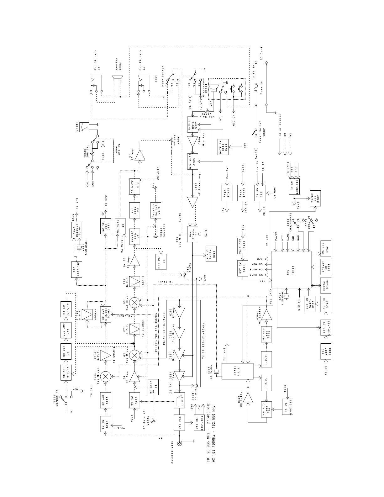
BLOCK DIAGRAM
— 5 —
Page 6
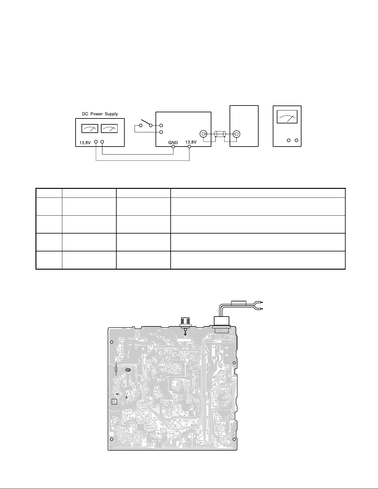
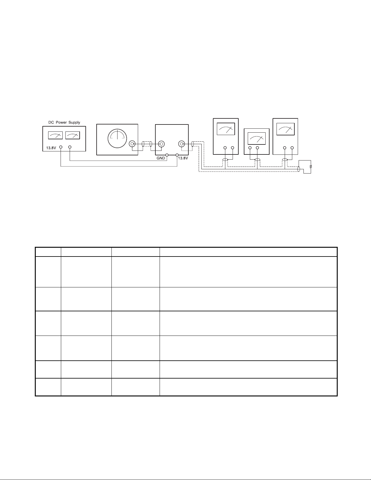
ALIGNMENT AND ADJUSTMENT
ALIGNMENT OF PLL
Test Equipment Required and Connections
• DC power supply: 13.8 V • DC voltmeter • Dummy load (50-ohm)
Dummy Load
(50-ohm)
And Attenuator
PTT
J751
MIC
JACK
Set
ANT
J501
Alignment Procedure
Step Preset to Adjustment Remarks
1 TX 40 CH L301 Adjust L301 to obtain 3.8 ±0.1 V (DC) at TP3 (R304).
DC Voltmeter
2 TX/RX 1 ~ 40 CH —
Check if the DC Voltage on all channels is kept within
1.5 V to 3.9 V at TP3.
3 RX 40 CH CT301 Adjust CT 301 to obtain 16.71 MHz ±50 Hz at TP7 (R216).
4 WX 1 ~ 7 CH —
Check if the DC Voltage on all channels is kept within
1.0 V to 4.0 V at TP4.
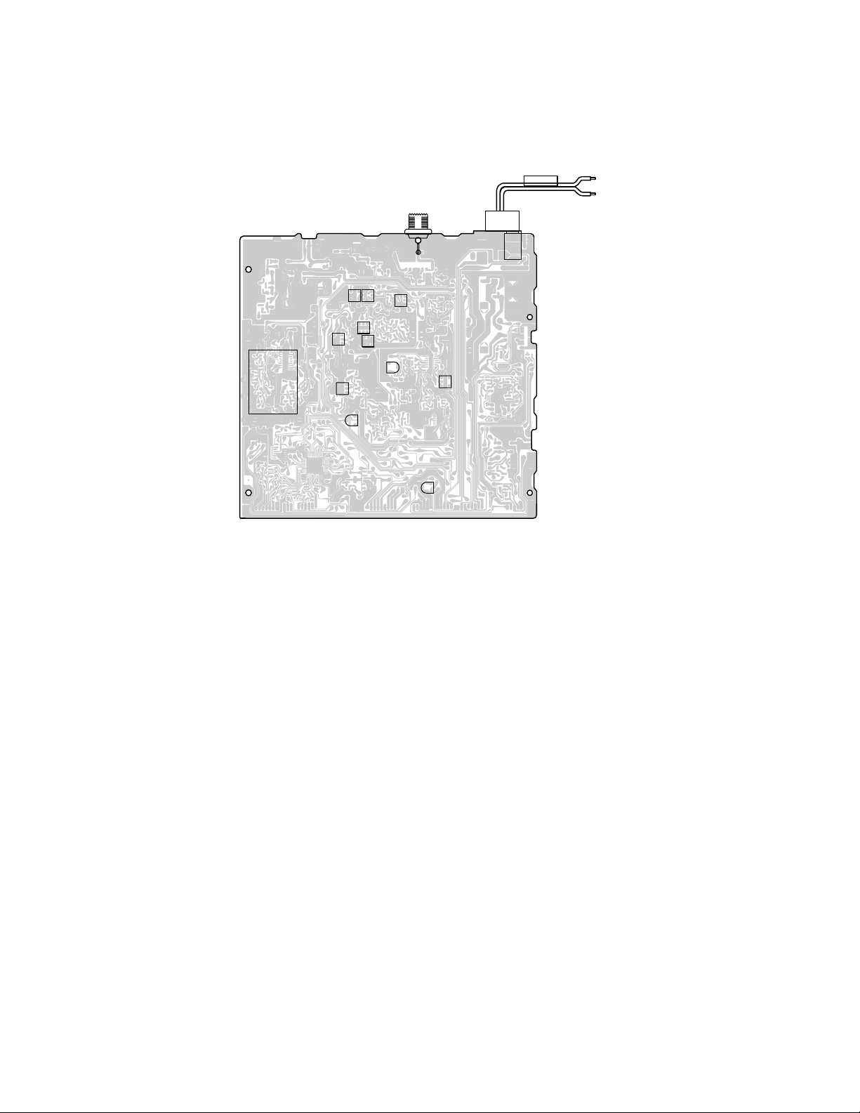
Alignment Point Locations (Main PCB)
TP7
R216
TP3
R304
L301
CT301
TP4
R325
ANT
J501
FUSE
DC CORD
WA901
J502
13.8v(RED)
GND(BLK)
— 6 —
Page 7
ALIGNMENT OF TRANSMITTER SECTION
Test Equipment Required and Connections
• DC power supply: 13.8 V • Modulation meter • AF oscillator
• RF power meter • Dummy load (50-ohm) & attenuator
AF Oscillator
PTT
Transceiver
RF Power Meter Modulation Meter
Dummy Load
(50-ohm)
And Attenuator
10 F
16V
MIC
+
4
Jack
5
J751
ANT
Jack
J501
Preset
• ALERT/WX/CB position: CB
Alignment Procedure
Step Preset to Adjustment Remarks
1
No modulation
19 CH
L205
2 No modulation — Confirm frequencies of all channels are within specification.
3 No modulation RT201
Adjust L205 by turning the core clockwise to obtain 3.8 W
reading on the RF power meter.
Adjust RT201 to position the indicator in the meter MT501
just on "SIG9".
Alignment Point Locations (Main PCB)
L205
RT201
ANT
J501
— 7 —
FUSE
DC CORD
WA901
J502
Microphone jack J751
13.8v(RED)
GND(BLK)
Page 8
ALIGNMENT OF RECEIVER SECTION
Test Equipment Required and Connections
• DC power supply: 13.8 V • AC voltmeter • Dummy load (8-ohm, 5 W resistive)
• Signal generator (SG) (27.205 MHz, 1 kHz, 30% AM modulation, output inpedance 50-ohm): CB
(162.45 MHz, 1 kHz, ±3kHz Dev. FM modulation, output impedance 50-ohm): WX
• SINAD Meter • Distortion meter
Signal Generator
Transceiver
ANT
Jack
J501
EXT.
SP.
J3
AC Voltmeter
Preset
• ALERT/WX/CB: CB
Alignment Procedure
Step Preset to Adjustment Remarks
Connect the SG to the antenna jack (J501) and the AC voltmeter
across the dummy load (8-ohm) to the external speaker jack (J3).
Adjust coil (L1 ~ L7) to obtain the maximum reading on the AC
voltmeter with keeping the level of the SG.
Set the output level of SG to 1 mV (−47 dBm).
Adjust coil L4 to obtain minimum Reading on the Distortion
Meter.
Set the output level of SG to 1 mV (−47 dBm).
Adjust RT1 so SQ just opens.
Set the output level of SG to 100 µV (−67 dBm).
Adjust RT2 to position the indicator in the meter MT501 just on
"SIG9".
Set the output level of SG to 100 µV (−67 dBm) No modulation.
Adjust coil to obtain the maximum reading on the AC voltmeter.
Set the output level of SG to SINAD 15 dB.
Adjust RT101 so SQ just opens.
1
Vol.: Max.
SQ.: Min.
RX: 20 CH
L3, L1, L7, L5
L6, L2
Vol.: Standard
2
SQ.: Min.
L4
RX: 20 CH
Vol.: Standard
20 CH
3
RT1
SQ.: Max.
Vol.: Standard
4
SQ.: Min.
RT2
RX: 20 CH
5 WX: 3 CH L103
6 WX: 3 CH RT101
SINAD Meter
Distortion Meter
Dummy Load
(8-ohm)
— 8 —
Page 9
Alignment Point Locations (Main PCB)
L2
L4
L7 L1
RT2
L5
L6
L3
RT101
ANT
J501
RT1
L103
FUSE
DC CORD
DC JACK J502
J3
13.8v(RED)
GND(BLK)
— 9 —
Page 10
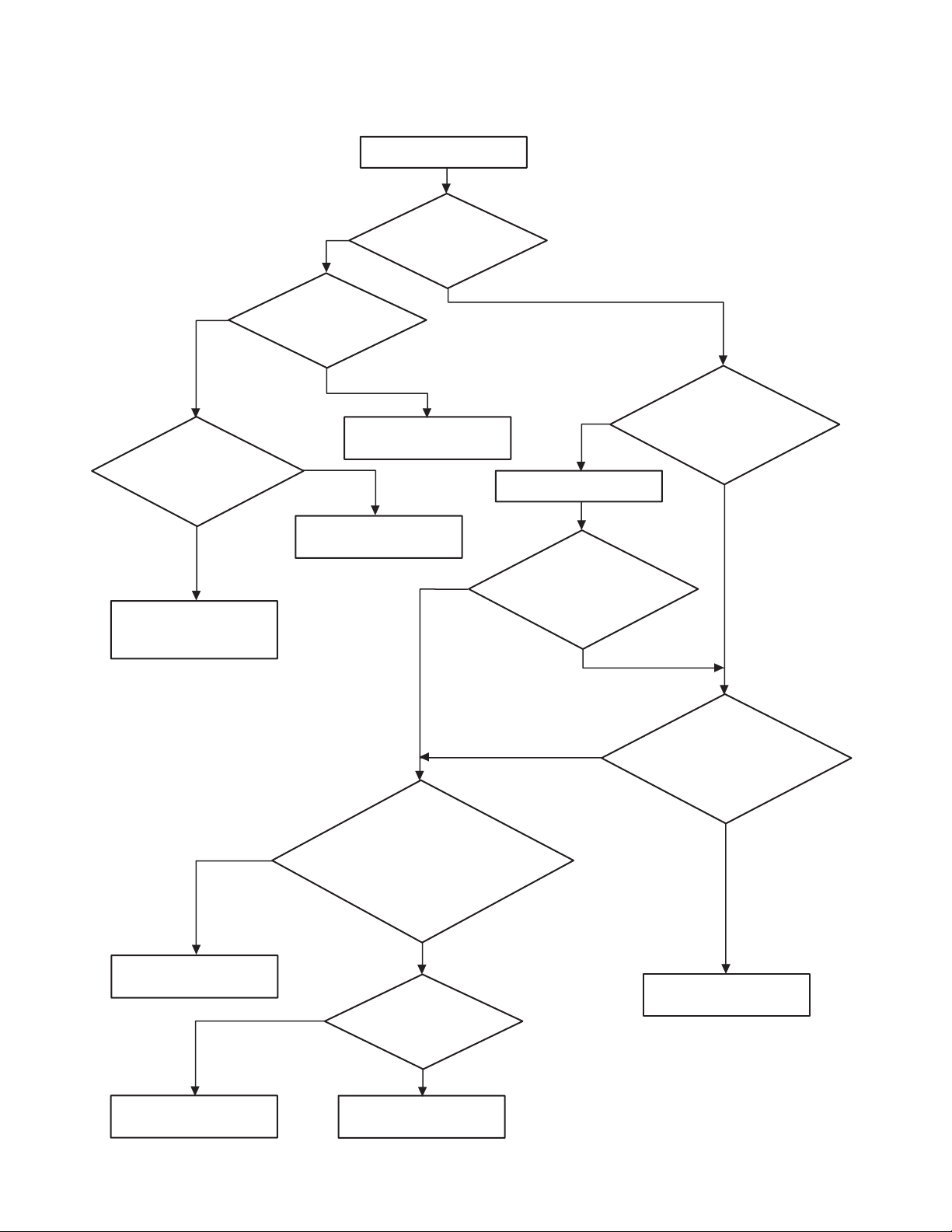
TROUBLESHOOTING
SYSTEM CONTROL SECTION CLOCK
Unit will not tum on
Power ON
OK
Is display normal?
OK
NG
Check the Fuse.
OK
Check the voltag
of IC502.
OK
NG
Check the voltage
at IC502.
OK
Check the
oscillation at pin
26 of IC401.
OK
NG
NG
e
NG
NG
Replace Fuse.
Check the power
SW VR601.
OK
Replace IC502.
Check the
voltage at pin 25
of IC401.
OK
NG
NG
Check the voltages
Replace IC502.
of IC403.
OK
NG
Replace IC403.
Check RX and TX
sections.
Check
the
voltages
of Q407, Q404
and Q405.
OK
Check the
soldering of the cable
between MAIN and FRONT
PCBs.
OK
Check the
voltage of D703.
OK
NG
NG
Check the
voltages of IC402
and Q401.
OK
Replace X401.
Replace Q407
and/or Q404, Q405.
NG
Replace soldering.
Replace D703.
— 10 —
NG
Replace IC402
and/or Q401.
Page 11
AUDIO SECTION
No RX sound
Check if
speaker wiring is
connected
properly.
OK
NG
Replace or resolder.
Check if
volume, squelch
controls are adjusted
properly.
OK
Check IC501
AF power IC and Q10.
OK
If CB
Check if Q7
voltages are as shown
in voltage chart.
OK
If PA
NG
NG
NG
Check volume and
wire connections.
OK
Adjust volume and
squelch control.
Replace IC501 AF power IC
and/or Q10.
Change CB/WX/PA
switch to PA.
ck Q7 and
Che
associated
circuit.
NG
Sound from
PA speaker?
Replace wire or resolder.
Connect PA speaker and PTT on.
Input 1kHz signal to MIC.
NG
OK
Check voltage
of Q204, Q206,
Q208, Q209.
NG
Replace
defective parts.
Check
Q6, 8, 9, and 12
voltages are as shown in
voltage
chart.
OK
Check RF section.
NG
Check microprocessor
section.
— 11 —
OK
Check PA
speaker
or CB/WX/PA switch
connection.
OK
Good.
PA function is good.
NG
Resolder.
Page 12
PLL CIRCUIT
CB No good
NG
Check whether voltage
reading at pin15 of
IC301 is approx. 5.0 V.
OK
Defective Q301, 302, 303
L301 or poor soldering.
NG
Check whether there
is RF voltage at pin11
of IC301.
OK
Defective R10, L101, C152
NG
Defective Vcc line (5.0 V) at
R316 or D303.
Check whether there
is RF voltage at
R58 (L7 side).
OK
or poor soldering.
NG
NG
Adjust L301.
Check whether there is
approx. 2.3 V at CH1 (RX) and
3.8 V at CH40 (TX) at TP3.
OK
approx. 2.3 V at CH1 (RX) and
3.8 V at CH40 (TX) at TP3.
Check whether there is
OK
NG
Defective IC401 or poor
soldering.
Defective crystal X301 or
poor soldering.
Check whether there are
pulses at pin13 of IC401 when
rotating the CH rotary switch upward, or
there are pulses at pin14 of IC401
when rotating the CH rotary
switch downward.
OK
NG
Check whether there is
RF voltage at
pin16 of IC301.
OK
Defective IC301 or poor
soldering.
— 12 —
NG
Check whether each channel
frequency matches the frequency
indicated in frequency chart.
OK
Good
PLL is not defective.
Page 13
PLL CIRCUIT
WX No good
Check
the voltage of
TP4 approx. 1 to 4V
at CH1~7.
OK
NG
Check
the voltage
reading at pin 15 of
IC301 is approx.
5 V.
OK
NG
Defective Vcc line at R316
or D303.
Check whether
each CH frequency matches
frequency indicated in
the
frequency chart.
OK
Check if there is RF
voltage at pin 16
of IC301.
Check the voltage Q305.
NG
pulse at pins 13 and 14 of IC401
when rotating the CH rotary
NG
OK
NG
OK
Check
whether there is a
SW top side and
down side.
OK
Defective xtal X301 or poor
soldering.
Defective Q305.
NG
between main and front wires
or check the channel switch.
Check the soldering
OK
Good PLL is not defective.
— 13 —
Page 14
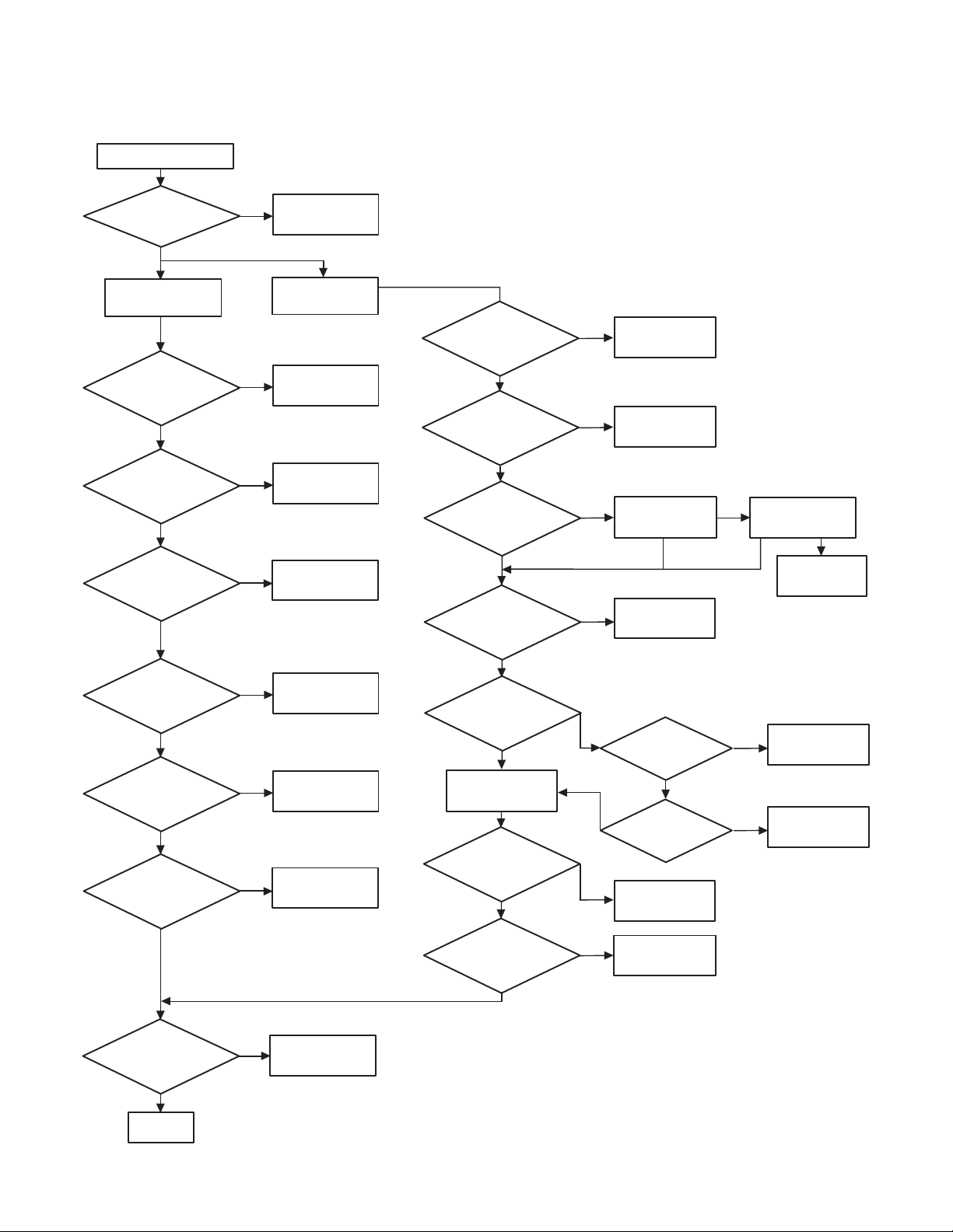
RX SECTION CHECK
Does not receive.
Check ANT jack.
OK
If C
B.
RF GAIN VOL MAX.
OK
Check
whether there is RF
voltage at TP7 and
2nd Local.
OK
Check the voltages
of Q6, 8 and 9.
OK
Check the voltages
of Q1 ~ Q5.
OK
Check the voltages
of D3.
OK
Check the voltages
of D202.
OK
Check the voltages
of Q11, D7, D8.
OK
NG
NG
NG
NG
NG
NG
NG
Replace J501.
NG
If WX/Digital
SAME.
See PLL section.
Replace
Q6, 8 and 9.
Replace
Q1 ~ Q5.
Replace
D3.
Replace
D202.
Replace
Q11, D7 or D8.
NG
Check the voltage
D201.
OK
Check the
voltage of TP4 1 to 4V
at WX C
H7.
OK
Check the voltage
at pin9 of IC102.
OK
Check the
waveform at Pin9
of IC102. (SSG
modulation
3 kHz)
OK
Check the WX SQ
operation.
OK
If the digital/SAME
OPERATION
OK
Check the voltages
at Q101 and 102.
OK
Check the voltages of
IC104.
NG
NG
NG
NG
NG
OK
NG
NG
Replace
D201.
See PLL section.
Adjust L103
(See page 8).
OK OK
Replace IC102.
Check the voltage
of D101.
OK
Check
the peripheral
circuit.
Replace
Q101 and 102.
Replace IC104.
Check the voltage
NG
at Pin 1 of IC102.
NG
NG
NG
Replace
IC102 or L103.
Replace D101.
Replace
defective parts.
Check the connection
of TP1.
OK
Good
NG
OK
Resolder TP1.
— 14 —
Page 15
TX SECTION CHECK
Does not transmit
Check the CB/WX
switch and the
connections.
OK
Check whether
TX LED turns on.
OK
NG
NG
Check the voltage at
pin 1 of IC401.
See PLL
section.
Defective or bad contact in
antenna connector, or defective
CB/WX switch.
NG
OK
NG
Check the
voltage at pin 10 of IC401.
(PTT ON: 5 V,
PTT OFF: 0 V)
OK
Check the
voltage at Pin 10 of IC301.
(PTT ON: 5V)
OK
NG
Check the
MIC and JACK.
OK
Check the
soldering between
Front and Main
PCBs.
OK
NG
NG
Change MIC.
Resolder.
Check the voltage
of Q501.
OK
Check the
voltages of Q201, 202
and Q203.
OK
Check the Modulation.
OK
Good
NG
NG
NG
Replace Q201, 202
Check the Microphone
voltage Q204, 205, 206,
Check the voltage at
Q402 and Q406.
OK
Replace Q501.
and/or Q203.
and MIC jack.
OK
Check the
Q207, 208, 209.
OK
Good
See system control section.
NG
NG
NG
Replace Microphone or
Replace defective parts.
Replace Q402 or Q406.
MIC jack.
— 15 —
Page 16
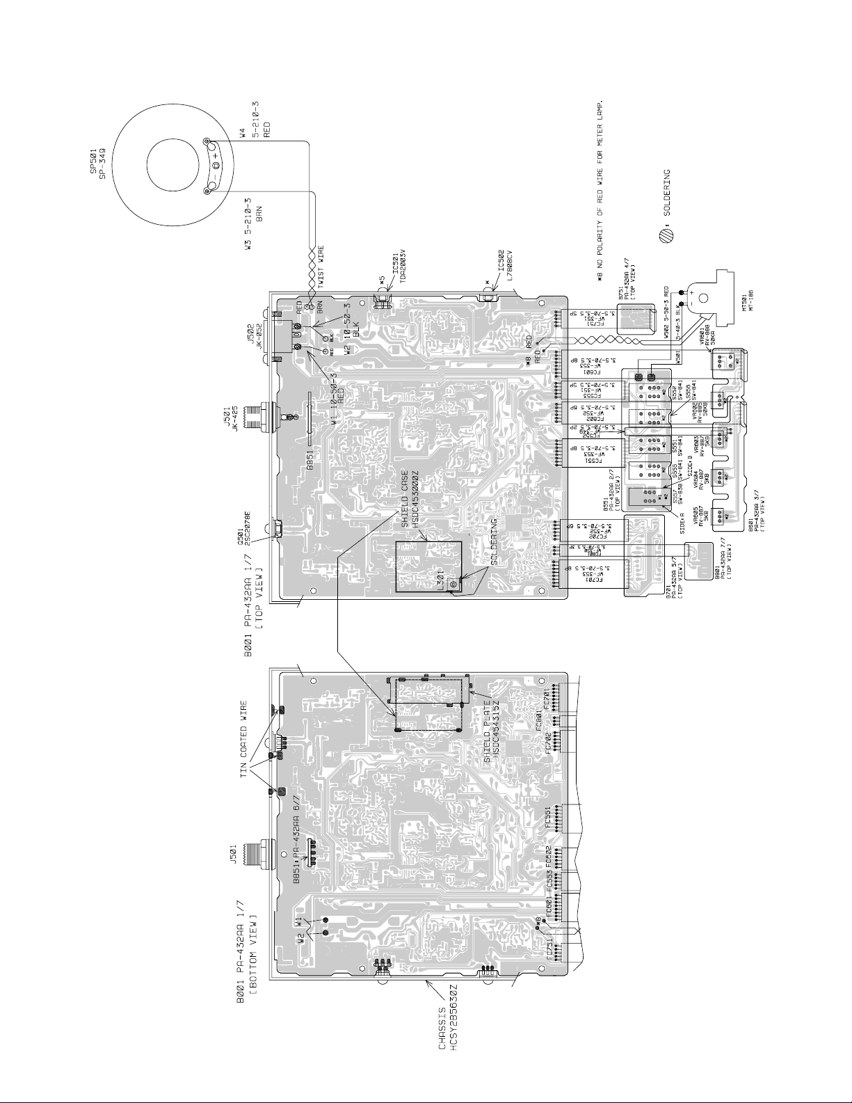
WIRING DIAGRAM
— 16 —
Page 17

Main
PRINTED CIRCUIT BOARDS
Top View
— 17 —
Page 18

Bottom View
— 18 —
Page 19

SWITCH/VOLUME/LED/MIC/CH SW/SWR PCBs
Top View Bottom View
— 19 —
Page 20

EXPLODED VIEW AND DISASSEMBLY INSTRUCTIONS
To remove the Top and Bottom Covers:
4
Remove eight screws
and Bottom Covers (see page 22).
20-3
from the both sides of Top
20-7
20-6
14
22
20-5
20-8
1
20-7
27
20-4
7
3
2
8
17
6
20-2
16
15
5
— 20 —
Page 21

26
20-1
21
9
5
10
13
— 21 —
Page 22

12
18
19
20-3
20-3
20-9
20-10
20-11
23
20-5
20-12
24
11
18
25
20-14
20-13
— 22 —
20-12
Page 23

MECHANICAL PARTS LIST
Ref. No. Description RS Part No. Mfr’ s Part No.
1 Shield Case SPTE,T=0.3 HSDC453000Z
2 Shield Plate SPTE HSDC454315Z
3 Cushion
4 Holder: PCB SECC HHDZ4B5754Z
5 Panel, Front ABS GCAS2B5626Z
6 Display Window PC GCAS442091Z
7 Holder, Meter POLYETHY,MILK WHITE GHDM404812Z
8 Holder, LED ABS GHDZ442085Z
9 Knob
10 Knob
11 Cover, Bottom VINY TOP HCAS2B5627Z
12 Cover, Top VINY TOP HCAS2B5628Z
13 Front Piece HCAS3B5629Z
14 Chassis SPCC HCSY2B5630Z
15 Chassis SECC HCSY3B5631Z
16 Himelon RBLD4B6084Z
17 Blind Plate PVC 0.4T BLACK RETC412489Z
18 Wool-Coated Paper, Wool Tack
19 Insulation Plate PVC,30*20*0.5T RZEB407154Z
20 Hardware Kit, Base HDWKT367ZHB
20-1 Screw, Flat HD + M3×4 NI SSCW133004N
20-2 Screw, Bind HD + M2.6×4 NI SSCW192604N
20-3 Screw, Bind HD + M3×5 NI SSCW193005N
20-4 Screw, Bind HD + M3×6 NI SSCW193006N
20-5 Screw, Bind HD + M3×8 NI SSCW193008N
20-6 Screw, Taptight Bind HD + M3×5 NI SSCW343005N
20-7 Screw, Taptight Bind HD + M3×6 NI SSCW343006N
20-8 Hex Nut M3.0 NI SSCW430030N
20-9 Nut, Flange M3 ZMC SSCW480030Z
20-10 Screw, Taptight Round HD + D3.5×8 NI SSCW293508N
20-11 Washer, Lock D3.5 NI SSCW530035N
20-12 Screw, Mounting ABS INST CLR BLACK GMSC405736A
20-13 Screw, Taptight Round HD + D5×10 NI SSCW295010N
20-14 Washer, Star D5 NI SSCW540050N
21 Spring Plate, Knob D6.02×L9.53 TSTD0200003
22 Cushion NEOPRENE RCUN4B6610Z
23 Hanger, Microphone SPCC,1.0T,NI HMHG402919Z
24 Mounting Bracket SPCC,1.6T,ZMC HBCT406058Z
25 Washer, Rubber EPT, BLACK 7×15×2.0T LWSR493891Z
26 Himelon RBLD451795Z
27 Cushion NEOPRENE RCUN451801Z
NEOPRENE SP 25*15*15T
ABS(PLATING),CR PLATING
ABS(PLATING),CR PLATING
WOOL PAPER,10*150*0.3T
RCUN435264Z
GNBZ442014Z
GNBZ442015Z
RUTC403865Z
— 23 —
Page 24

ELECTRICAL PARTS LIST
MAIN PCB ASSEMBLY
Ref. No. Description RS Part No. Mfr’s Part No.
B1 AT367ZHBA
Capacitors
C1 Ceramic 15 pF 50 V ±5 % CH BCMM811504Z
C2 Ceramic 220 pF 50 V ±5 % CH BCMM812214Z
C3 Ceramic 470 pF 50 V ±5 % CH BCMM814714Z
C4 Electrolytic 4.7 µF 50 V ±20 % C-156 BCAZ814796Z
C5 Ceramic 0.001 µF 50 V ±10 % B BCML811025Z
C6 Ceramic 0.01 µF 50 V ±10 % B BCML811035Z
C7 Ceramic 0.01 µF 50 V ±10 % B BCML811035Z
C8 Ceramic 220 pF 50 V ±5 % CH BCMM812214Z
C9 Ceramic 0.0022 µF 50 V ±10 % B BCML812225Z
C10 Ceramic 0.01 µF 50 V ±10 % B BCML811035Z
C11 Ceramic 0.001 µF 50 V ±10 % B BCML811025Z
C12 Ceramic 0.022 µF 25 V ±10 % B BCML512235Z
C13 Ceramic 33 pF 50 V ±5 % CH BCMM813304Z
C14 Ceramic 0.047 µF 50 V ±10 % B BCML814735Z
C15 Ceramic 0.001 µF 50 V ±10 % B BCML811025Z
C16 Ceramic 0.0047 µF 50 V ±10 % B BCML814725Z
C17 Electrolytic 0.47 µF 50 V ±20 % C-156 BCAZ814786Z
C18 Ceramic 0.47 µF 10 V ±10 % B BCML114745Z
C19 Electrolytic 4.7 µF 50 V ±20 % C-156 BCAZ814796Z
C20 Ceramic 0.01 µF 50 V ±10 % B BCML811035Z
C21 Ceramic 0.0047 µF 50 V ±10 % B BCML814725Z
C22 Electrolytic 4.7 µF 50 V ±20 % C-156 BCAZ814796Z
C23 Ceramic 0.022 µF 25 V ±10 % B BCML512235Z
C24 Ceramic 0.01 µF 50 V ±10 % B BCML811035Z
C25 Ceramic 0.01 µF 50 V ±10 % B BCML811035Z
C26 Ceramic 1 µF 6.3 V ±10 % B BCML901055Z
C27 Ceramic 220 pF 50 V ±5 % CH BCMM812214Z
C28 Ceramic 0.001 µF 50 V ±10 % B BCML811025Z
C29 Ceramic 0.0047 µF 50 V ±10 % B BCML814725Z
C30 Electrolytic 100 µF 10 V ±20 % C-156 BCAZ111016Z
C31 Electrolytic 470 µF 16 V ±20 % C-156 BCAZ314716Z
C32 Ceramic 0.01 µF 50 V ±10 % B BCML811035Z
C33 Electrolytic 1000 µF 25 V ±20 % C-156 BCAZ511026Z
C34 Ceramic 0.1 µF 16 V ±10 % B BCML311045Z
C35 Electrolytic 47 µF 25 V ±20 % C-155 BCAK514706Z
C36 Ceramic 0.001 µF 50 V ±10 % B BCML811025Z
C37 Ceramic 0.001 µF 50 V ±10 % B BCML811025Z
C38 Ceramic 5 pF 50 V ±0.25 pF CH BCMM815091Z
C39 Electrolytic 100 µF 10 V ±20 % C-156 BCAZ111016Z
C40 Ceramic 0.01 µF 50 V ±10 % B BCML811035Z
C41 Ceramic 0.01 µF 50 V ±10 % B BCML811035Z
C42 Ceramic 3 pF 50 V ±0.1 pF CH BCMM813098Z
C43 Ceramic 0.01 µF 50 V ±10 % B BCML811035Z
C44 Ceramic 0.001 µF 50 V ±10 % B BCML811025Z
Assembly, MAIN PCB
Consists of the following:
Notes: All ceramic capacitors are Multilayer (1608) Tape type, unless otherwise specified.
The following codes indicate variations of capacitors against temperature:
B=±10%, CH=0±60 ppm/°C, UJ=−750 ppm/°C±120 ppm/°C, CK=0 ±250 ppm/°C,
F=+30 −80 %,
— 24 —
Page 25

Ref. No. Description RS Part No. Mfr’s Part No.
C45 Ceramic 100 pF 50 V ±5 % CH BCMM811014Z
C46 Ceramic 0.001 µF 50 V ±10 % B BCML811025Z
C47 Ceramic 150 pF 50 V ±5 % CH BCMM811514Z
C48 Ceramic 0.001 µF 50 V ±10 % B BCML811025Z
C49 Ceramic 0.022 µF 25 V ±10 % B BCML512235Z
C50 Ceramic 0.01 µF 50 V ±10 % B BCML811035Z
C51 Electrolytic 1 µF 50 V ±20 % C-156 BCAZ811096Z
C52 Ceramic 0.01 µF 50 V ±10 % B BCML811035Z
C53 Ceramic 0.01 µF 50 V ±10 % B BCML811035Z
C54 Electrolytic 22 µF 50 V ±20 % C-156 BCAZ812206Z
C55 Ceramic 1.5 pF 50 V ±0.25 pF CK BCMS811591Z
C56 Electrolytic 1 µF 50 V ±20 % C-156 BCAZ811096Z
C57 Electrolytic 10 µF 50 V ±20 % C-156 BCAZ811006Z
C58 Ceramic 100 pF 50 V ±5 % CH BCMM811014Z
C59 Ceramic 0.1 µF 16 V ±10 % B BCML311045Z
C60 Electrolytic 22 µF 50 V ±20 % C-156 BCAZ812206Z
C61 Ceramic 0.01 µF 50 V ±10 % B BCML811035Z
C62 Not Used
C63 Ceramic 1 µF 6.3 V ±10 % B BCML901055Z
C64 Ceramic 1 µF 6.3 V ±10 % B BCML901055Z
C65 Ceramic 0.047 µF 50 V ±10 % B BCML814735Z
C66~100 Not Used
C101 Ceramic 4 pF 50 V ±0.25 pF CH BCMM814091Z
C102 Ceramic 4 pF 50 V ±0.25 pF CH BCMM814091Z
C103 Ceramic 2 pF 50 V ±0.25 pF CH BCMV812098Z
C104 Ceramic 0.01 µF 50 V ±10 % B BCML811035Z
C105 Ceramic 22 pF 50 V ±5 % CH BCMM812204Z
C106 Ceramic 0.001 µF 50 V ±10 % B BCML811025Z
C107 Ceramic 0.01 µF 50 V ±10 % B BCML811035Z
C108 Ceramic 0.1 µF 16 V ±10 % B BCML311045Z
C109 Not Used
C110 Ceramic 0.047 µF 50 V ±10 % B BCML814735Z
C111 Ceramic 0.047 µF 50 V ±10 % B BCML814735Z
C112 Ceramic 0.01 µF 50 V ±10 % B BCML811035Z
C113 Ceramic 470 pF 50 V ±5 % CH BCMM814714Z
C114 Ceramic 470 pF 50 V ±5 % CH BCMM814714Z
C115 Ceramic 0.01 µF 50 V ±10 % B BCML811035Z
C116 Ceramic 0.0082 µF 50 V ±10 % B BCML818225Z
C117 Ceramic 7 pF 50 V ±0.5 pF CH BCMM817092Z
C118 Not Used
C119 Ceramic 330 pF 50 V ±5 % CH BCMM813314Z
C120 Ceramic 0.01 µF 50 V ±10 % B BCML811035Z
C121 Ceramic 0.01 µF 50 V ±10 % B BCML811035Z
C122 Ceramic 150 pF 50 V ±5 % CH BCMM811514Z
C123 Not Used
C124 Ceramic 0.0047 µF 50 V ±10 % B BCML814725Z
C125 Ceramic 1 µF 6.3 V ±10 % B BCML901055Z
C126 Ceramic 0.01 µF 50 V ±10 % B BCML811035Z
C127 Ceramic 47 pF 50 V ±5 % CH BCMM814704Z
C128 Ceramic 3 pF 50 V ±0.1 pF CH BCMM813098Z
C129 Ceramic (2125) 1 µF 10 V ±10 % B BCXT111055Z
C130 Ceramic (2125) 1 µF 10 V ±10 % B BCXT111055Z
C131 Ceramic 120 pF 50 V ±5 % CH BCMM811214Z
— 25 —
Page 26

Ref. No. Description RS Part No. Mfr’s Part No.
C132 Ceramic 0.047 µF 50 V ±10 % B BCML814735Z
C133 Ceramic 0.001 µF 50 V ±10 % B BCML811025Z
C134 Ceramic 0.01 µF 50 V ±10 % B BCML811035Z
C135 Not Used
C136 Electrolytic 2.2 µF 50 V ±20 % C-156 BCAZ812296Z
C137 Ceramic 0.0047 µF 50 V ±10 % B BCML814725Z
C138 Electrolytic 1 µF 50 V ±20 % C-156 BCAZ811096Z
C139 Ceramic 330 pF 50 V ±5 % CH BCMM813314Z
C140 Ceramic 0.0018 µF 50 V ±10 % B BCML811825Z
C141 Ceramic 0.1 µF 16 V ±10 % B BCML311045Z
C142 Ceramic 100 pF 50 V ±5 % CH BCMM811014Z
C143 Ceramic 0.01 µF 50 V ±10 % B BCML811035Z
C144 Not Used
C145 Ceramic 0.0012 µF 50 V ±10 % B BCML811225Z
C146 Not Used
C147 Ceramic 0.0056 µF 50 V ±10 % B BCML815625Z
C148 Ceramic 0.1 µF 16 V ±10 % B BCML311045Z
C149 Not Used
C150 Ceramic 22 pF 50 V ±5 % CH BCMM812204Z
C151 Ceramic 22 pF 50 V ±5 % CH BCMM812204Z
C152 Ceramic 22 pF 50 V ±5 % CH BCMM812204Z
C153 Ceramic 100 pF 50 V ±5 % CH BCMM811014Z
C154 Ceramic 100 pF 50 V ±5 % CH BCMM811014Z
C155~199 Not Used
C200 Ceramic 9 pF 50 V ±0.5 pF CH BCMM819092Z
C201 Ceramic 0.001 µF 50 V ±10 % B BCML811025Z
C202 Not Used
C203 Ceramic 180 pF 50 V ±5 % CH BCMM811814Z
C204 Ceramic 270 pF 50 V ±5 % CH BCMM812714Z
C205 Ceramic 27 pF 50 V ±5 % CH BCMM812704Z
C206 Ceramic 180 pF 50 V ±5 % CH BCMM811814Z
C207 Ceramic 0.001 µF 50 V ±10 % B BCML811025Z
C208 Ceramic 27 pF 50 V ±5 % CH BCMM812704Z
C209 Ceramic 0.047 µF 50 V ±10 % B BCML814735Z
C210 Ceramic 15 pF 50 V ±5 % CH BCMM811504Z
C211 Ceramic 10 pF 50 V ±0.5 pF CH BCMM811002Z
C212 Ceramic 220 pF 50 V ±5 % CH BCMM812214Z
C213 Ceramic 27 pF 50 V ±5 % CH BCMM812704Z
C214 Ceramic 0.01 µF 50 V ±10 % B BCML811035Z
C215 Ceramic 0.01 µF 50 V ±10 % B BCML811035Z
C216 Ceramic 470 pF 50 V ±5 % CH BCMM814714Z
C217 Ceramic 0.001 µF 50 V ±10 % B BCML811025Z
C218 Ceramic 100 pF 50 V ±5 % CH BCMM811014Z
C219 Ceramic 0.001 µF 50 V ±10 % B BCML811025Z
C220 Electrolytic 100 µF 10 V ±20 % C-156 BCAZ111016Z
C221 Ceramic 0.047 µF 50 V ±10 % B BCML814735Z
C222 Ceramic 0.047 µF 50 V ±10 % B BCML814735Z
C223 Ceramic 0.01 µF 50 V ±10 % B BCML811035Z
C224 Ceramic 2 pF 50 V ±0.1 pF CH BCMM812098Z
C225 Electrolytic 47 µF 25 V ±20 % C-156 BCAZ514706Z
C226 Ceramic 0.047 µF 50 V ±10 % B BCML814735Z
C227 Ceramic 0.01 µF 50 V ±10 % B BCML811035Z
C228 Electrolytic 1 µF 50 V ±20 % C-156 BCAZ811096Z
— 26 —
Page 27

Ref. No. Description RS Part No. Mfr’s Part No.
C229 Ceramic 0.022 µF 25 V ±10 % B BCML512235Z
C230 Ceramic 150 pF 50 V ±5 % CH BCMM811514Z
C231 Ceramic 0.0047 µF 50 V ±10 % B BCML814725Z
C232 Electrolytic 22 µF 50 V ±20 % C-156 BCAZ812206Z
C233 Electrolytic 22 µF 50 V ±20 % C-156 BCAZ812206Z
C234 Ceramic 0.047 µF 16 V ±10 % B BCML314735Z
C235 Ceramic 0.022 µF 25 V ±10 % B BCML512235Z
C236 Ceramic 47 pF 50 V ±5 % CH BCMM814704Z
C237 Ceramic 0.01 µF 50 V ±10 % B BCML811035Z
C238 Ceramic 0.0047 µF 50 V ±10 % B BCML814725Z
C239 Electrolytic 47 µF 25 V ±20 % C-156 BCAZ514706Z
C240 Ceramic 0.001 µF 50 V ±10 % B BCML811025Z
C241 Ceramic 0.01 µF 50 V ±10 % B BCML811035Z
C242 Ceramic 0.001 µF 50 V ±10 % B BCML811025Z
C243 Ceramic 0.001 µF 50 V ±10 % B BCML811025Z
C244 Ceramic 0.001 µF 50 V ±10 % B BCML811025Z
C245, 246 Not Used
C247 Ceramic 0.01 µF 50 V ±10 % B BCML811035Z
C248 Ceramic 0.01 µF 50 V ±10 % B BCML811035Z
C249~300 Not Used
C301 Ceramic 0.01 µF 50 V ±10 % B BCML811035Z
C302 Electrolytic 47 µF 25 V ±20 % C-156 BCAZ514706Z
C303 Ceramic 0.01 µF 50 V ±10 % B BCML811035Z
C304 Ceramic 15 pF 50 V ±5 % CH BCMM811504Z
C305 Ceramic 150 pF 50 V ±5 % CH BCMM811514Z
C306 Ceramic 330 pF 50 V ±5 % CH BCMM813314Z
C307 Ceramic 22 pF 50 V ±5 % CH BCMM812204Z
C308 Ceramic 56 pF 50 V ±5 % UJ BCMP815604Z
C309 Ceramic 0.01 µF 50 V ±10 % B BCML811035Z
C310
Semi Conductor (YR) TS 2.5 S
0.022 µF 25 V ±10 % TAPING BCGL512235Z
C311 Ceramic 1 µF 6.3 V ±10 % B BCML901055Z
C312 Electrolytic 0.47 µF 50 V ±20 % C-094 BCEU814786Z
C313 Ceramic 68 pF 50 V ±5 % CH BCMM816804Z
C314 Ceramic 0.001 µF 50 V ±10 % B BCML811025Z
C315 Ceramic 390 pF 50 V ±5 % CH BCMM813914Z
C316 Ceramic 0.1 µF 16 V ±10 % B BCML311045Z
C317 Ceramic 7 pF 50 V ±0.5 pF CH BCMM817092Z
C318 Ceramic 22 pF 50 V ±5 % CH BCMM812204Z
C319 Ceramic 27 pF 50 V ±5 % CH BCMM812704Z
C320 Ceramic 8 pF 50 V ±0.5 pF CH BCMM818092Z
C321 Ceramic 0.001 µF 50 V ±10 % B BCML811025Z
C322 Ceramic 27 pF 50 V ±5 % CH BCMM812704Z
C323 Electrolytic 220 µF 10 V ±20 % C-156 BCAZ112216Z
C324
Semi Conductor (YR) TS 2.5 S
0.01 µF 25 V ±10 % TAPING BCGL511035Z
C325 Electrolytic 0.47 µF 50 V ±20 % C-094 BCEU814786Z
C326 Electrolytic 100 µF 10 V ±20 % C-156 BCAZ111016Z
C327 Ceramic 33 pF 50 V ±5 % CH BCMM813304Z
C328 Ceramic 0.001 µF 50 V ±10 % B BCML811025Z
C329
C330
Semi Conductor (YR) TS 5.0 S
Semi Conductor (YR) TS 5.0 S
0.047 µF 25 V ±10 % TAPING BCGL514735Z
0.047 µF 25 V ±10 % TAPING BCGL514735Z
C331 Electrolytic 4.7 µF 50 V ±20 % C-156 BCAZ814796Z
C332 Ceramic 56 pF 50 V ±5 % CH BCMM815604Z
C333 Ceramic 47 pF 50 V ±5 % CH BCMM814704Z
— 27 —
Page 28

Ref. No. Description RS Part No. Mfr’s Part No.
C334 Ceramic 0.1 µF 16 V ±10 % B BCML311045Z
C335 Ceramic 0.001 µF 50 V ±10 % B BCML811025Z
C336 Ceramic 0.1 µF 16 V ±10 % B BCML311045Z
C337 Ceramic 0.1 µF 25 V −20+80 % F BCMF511040Z
C338 Ceramic 1 µF 10 V −20+80 % F BCMF111050Z
C339 Ceramic 0.001 µF 50 V ±10 % B BCML811025Z
C340~400 Not Used
C401 Ceramic 0.047 µF 50 V ±10 % B BCML814735Z
C402 Electrolytic 47 µF 25 V ±20 % C-156 BCAZ514706Z
C403 Ceramic 0.1 µF 16 V ±10 % B BCML311045Z
C404 Ceramic 0.1 µF 16 V ±10 % B BCML311045Z
C405 Electrolytic 22 µF 50 V ±20 % C-156 BCAZ812206Z
C406 Ceramic 0.22 µF 10 V ±10 % B BCML112245Z
C407 Ceramic 0.1 µF 16 V ±10 % B BCML311045Z
C408 Ceramic 0.047 µF 50 V ±10 % B BCML814735Z
C409 Ceramic 0.047 µF 50 V ±10 % B BCML814735Z
C410 Ceramic 0.01 µF 50 V ±10 % B BCML811035Z
C411 Ceramic 0.01 µF 50 V ±10 % B BCML811035Z
C412 Ceramic 22 pF 50 V ±5 % CH BCMM812204Z
C413 Ceramic 22 pF 50 V ±5 % CH BCMM812204Z
C414 Ceramic 0.022 µF 25 V ±10 % B BCML512235Z
C415 Electrolytic 100 µF 10 V ±20 % C-156 BCAZ111016Z
C416 Electrolytic 1000 µF 16 V ±20 % C-156 BCAZ311026Z
C417 Ceramic 0.47 µF 10 V ±10 % B BCML114745Z
C418 Ceramic 1 µF 6.3 V ±10 % B BCML901055Z
C419 Ceramic 0.022 µF 25 V ±10 % B BCML512235Z
C420 Ceramic 0.001 µF 50 V ±10 % B BCML811025Z
C421 Ceramic 0.1 µF 16 V ±10 % B BCML311045Z
C422, 423 Not Used
C424 Ceramic 0.047 µF 50 V ±10 % B BCML814735Z
C425 Ceramic 0.01 µF 50 V ±10 % B BCML811035Z
C426 Electrolytic 10 µF 50 V ±20 % C-156 BCAZ811006Z
C427 Electrolytic 100 µF 10 V ±20 % C-156 BCAZ111016Z
C428 Ceramic 0.001 µF 50 V ±10 % B BCML811025Z
C429 Ceramic 0.001 µF 50 V ±10 % B BCML811025Z
C430 Ceramic 0.001 µF 50 V ±10 % B BCML811025Z
CT301 Trimmer CT-090 ECR-LA050M52 50 pF BCTY0090500
Diodes
D1 1N4148 T-77 AX TS 26+ BDAY0246003
D2 1N4148 T-77 AX TS 26+ BDAY0246003
D3 1N4148 T-77 AX TS 26+ BDAY0246003
D4 1SS390 TE61 BDAY1041001
D5 HSM88AS TL BDAY0346001
D6 1SS108 TD AX TS 26+ BDAY0798001
D7 1N4148 T-77 AX TS 26+ BDAY0246003
D8 1N4148 T-77 AX TS 26+ BDAY0246003
D9 1N4148 T-77 AX TS 26+ BDAY0246003
D10 1N4148 T-77 AX TS 26+ BDAY0246003
D11 1N4148 T-77 AX TS 26+ BDAY0246003
D12 1N4148 T-77 AX TS 26+ BDAY0246003
D13~100 Not Used
— 28 —
Page 29

Ref. No. Description RS Part No. Mfr’s Part No.
D101 HSM88AS TL BDAY0346001
D102~104 Not Used
D105 1N4148 T-77 AX TS 26+ BDAY0246003
D106 1N4148 T-77 AX TS 26+ BDAY0246003
D107~200 Not Used
D201 Switching 1SS356 TW11 BDAY0808001
D202 Switching 1SS356 TW11 BDAY0808001
D203 1N4148 T-77 AX TS 26+ BDAY0246003
D204 1N4148 T-77 AX TS 26+ BDAY0246003
D205 1N4003 BDAY0133001
D206 1N4148 T-77 AX TS 26+ BDAY0246003
D207, 208 Not Used
D209 1N4148 T-77 AX TS 26+ BDAY0246003
D210~300 Not Used
D301 Varicap HVU307 TRU BDAY0940001
D302 Varicap HVU307 TRU BDAY0940001
D303 Zener HZ5B1 TD AX TS 26+ BDAY0492040
D304~405 Not Used
D406 1N4003 BDAY0133001
D407 1N4148 T-77 AX TS 26+ BDAY0246003
D408 Zener HZ5C1 TD AX TS 26+ BDAY0492002
Filter
FT1 Ceramic FL-048 SFELA10M7GM00-B0 BFLY0048001
FT2 Ceramic FL-852 LTS455HTW BFLY0852001
FT3~100 Not Used
FT101 Ceramic FL-048 SFELA10M7GM00-B0 BFLY0048001
FT102 Ceramic FL-743 LTW33-455D BFLY0743001
FT103 Ceramic FL-743 LTW33-455D BFLY0743001
ICs
IC101 Not Used
IC102 S1T3361D01-S0T0 BDEY3282003
IC103 Not Used
IC104 SM8224CM-E2 BDEY3021003
IC301 BU2630F-E2 BDEY2769003
IC401 UC2891 UPD789166GB-685-8ES BDDY1435001
IC402 XC61CC4302PR/XC61AC4302PR BDEY4017003
IC403 RH5RL50AA-T1 BDEY2935003
IC404 Not Used
IC405 AT24CO2N-10SI-1.8 BDEY3517003
Jack
J1, 2 Not Used
J3 Earphone JK-899 JH3501-020D BJKY0899001
J4 Earphone JK-899 JH3501-020D BJKY0899001
— 29 —
Page 30

Ref. No. Description RS Part No. Mfr’s Part No.
Coil
L1 LB-1030 K7T1/33333 BLBY1030001
L2 LB-1029 K7-H5/33333 BLBY1029001
L3 LB-1103 M7-M/33303 BLBY1103001
L4 LB-1028 K7-H5/33333 BLBY1028001
L5 LB-652 M7-M/33334 BLBY0652001
L6 LB-652 M7-M/33334 BLBY0652001
L7 LB-1030 K7T1/33333 BLBY1030001
L101 Inductor Molded LZ-041 1 µH K BLZY0041109
L102
Inductor Molded Chip Tape
LZ-183 HK1608R10J-T 100NH BLZY0183108
L103 LB-1175 7002BE-A0026HM BLBY1175001
L104 LE-278 7T 0.5UEW BLEY0278001
L105 Not Used
L106
L107 Inductor Molded LZ-041
Inductor Molded Chip Tape
LZ-183 HK1608R10J-T 100NH BLZY0183108
1.8 µH K
BLZY0041189
L201 Not Used
L202 LE-417 L-2E4-S(R22-E712X) BLEY0417001
L203 LE-419 L-1E4-S(R22-E813) BLEY0419001
L204 LE-435 L-1E4-S(R22-E858) BLEY0435001
L205 LC-228 L-1S7-T(R12-J840X) BLCY0228001
L206 LD-237 L-2R4W(R22-E563) BLDY0237001
L207 LD-087 BF04-3*5*1 BLDY0087001
L208 LE-535 BLEY0535001
L209 LD-087 BF04-3*5*1 BLDY0087001
L210 Inductor Molded LZ-041
0.47 µH K
BLZY0041478
L301 LB-1112 M7-D3/31332 BLBY1112001
L302 Inductor Molded LZ-041 1 µH K BLZY0041109
L303 Inductor Molded Chip LZ-219 LLQ2012-E47NJ 47N BLZY0219477
Transistor
Q1 DB-718 2SC2714-Y TE85L BDBC2714124
Q2 DB-718 2SC2714-Y TE85L BDBC2714124
Q3 DB-718 2SC2714-Y TE85L BDBC2714124
Q4 DB-718 2SC2714-Y TE85L BDBC2714124
Q5 DB-862 2SC3052-T12-1F BDBC3052106
Q6 DB-862 2SC3052-T12-1F BDBC3052106
Q7 DB-862 2SC3052-T12-1F BDBC3052106
Q8 DB-862 2SC3052-T12-1F BDBC3052106
Q9 DB-862 2SC3052-T12-1F BDBC3052106
Q10 DB-862 2SC3052-T12-1F BDBC3052106
Q11 DB-862 2SC3052-T12-1F BDBC3052106
Q12 DB-862 2SC3052-T12-1F BDBC3052106
Q13 DB-718 2SC2714-Y TE85L BDBC2714124
Q14 DB-718 2SC2714-Y TE85L BDBC2714124
Q15 DB-035 2SA812(M)-M6A T1B BDBA0812695
Q16 DB-862 2SC3052-T12-1F BDBC3052106
Q17 DB-092 2SA1235A-T12-1F BDBA1235106
Q18 DB-862 2SC3052-T12-1F BDBC3052106
Q101 DB-862 2SC3052-T12-1F BDBC3052106
Q102 DB-862 2SC3052-T12-1F BDBC3052106
Q103 DB-848 2SC5065-Y(TE85R) BDBC5065124
— 30 —
Page 31

Ref. No. Description RS Part No. Mfr’s Part No.
Q104 DB-848 2SC5065-Y(TE85R) BDBC5065124
Q201 DB-792 2SC2314F BDBC2314106
Q202 DB-301 2SC941TM-O TAPING RH TS+ BDBX0941523
Q203 DB-718 2SC2714-Y TE85L BDBC2714124
Q204 DB-862 2SC3052-T12-1F BDBC3052106
Q205 DB-092 2SA1235A-T12-1F BDBA1235106
Q206 DB-862 2SC3052-T12-1F BDBC3052106
Q207 DB-862 2SC3052-T12-1F BDBC3052106
Q208 DB-092 2SA1235A-T12-1F BDBA1235106
Q209 DB-862 2SC3052-T12-1F BDBC3052106
Q301 DB-718 2SC2714-Y TE85L BDBC2714124
Q302 DB-718 2SC2714-Y TE85L BDBC2714124
Q303 DB-862 2SC3052-T12-1F BDBC3052106
Q304 DB-718 2SC2714-Y TE85L BDBC2714124
Q305 DB-718 2SC2714-Y TE85L BDBC2714124
Q306 DB-862 2SC3052-T12-1F BDBC3052106
Q401 DB-862 2SC3052-T12-1F BDBC3052106
Q402 DB-035 2SA812(M)-M6A T1B BDBA0812695
Q403 Not Used
Q404 DB-035 2SA812(M)-M6A T1B BDBA0812695
Q405 DB-035 2SA812(M)-M6A T1B BDBA0812695
Q406 DB-862 2SC3052-T12-1F BDBC3052106
Q407 DB-309 2SC2001-L BDBC2001111
Q408 DB-092 2SA1235A-T12-1F BDBA1235106
Q409 DB-092 2SA1235A-T12-1F BDBA1235106
Q410 DB-092 2SA1235A-T12-1F BDBA1235106
Q411 DB-092 2SA1235A-T12-1F BDBA1235106
Q412 DB-092 2SA1235A-T12-1F BDBA1235106
Q413 DB-092 2SA1235A-T12-1F BDBA1235106
Q414 DB-092 2SA1235A-T12-1F BDBA1235106
Resistors
R1 Carbon Fixed Chip 1.5 kohm 1/16 W ±5 % BRFC161524Z
R2 Carbon Fixed Chip 4.7 kohm 1/16 W ±5 % BRFC164724Z
R3 Carbon Fixed Chip 5.6 kohm 1/16 W ±5 % BRFC165624Z
R4 Carbon Fixed Chip 330 ohm 1/16 W ±5 % BRFC163314Z
R5 Carbon Fixed Chip 56 ohm 1/16 W ±5 % BRFC165604Z
R6 Carbon Fixed Chip 3.3 kohm 1/16 W ±5 % BRFC163324Z
R7 Carbon Fixed Chip 560 ohm 1/16 W ±5 % BRFC165614Z
R8 Carbon Fixed Chip 820 ohm 1/16 W ±5 % BRFC168214Z
R9
Carbon Axial Lead (26)
100 ohm 1/6 W ±5 % BRPA611014Z
R10 Not Used
R11 Carbon Fixed Chip 8.2 kohm 1/16 W ±5 % BRFC168224Z
R12 Carbon Fixed Chip 180 ohm 1/16 W ±5 % BRFC161814Z
R13
R14
R15
Carbon Axial Lead (26)
Carbon Axial Lead (26)
Carbon Axial Lead (26)
100 ohm 1/6 W ±5 % BRPA611014Z
270 kohm 1/6 W ±5 % BRPA612744Z
220 ohm 1/6 W ±5 % BRPA612214Z
R16 Carbon Fixed Chip 560 ohm 1/16 W ±5 % BRFC165614Z
R17 Carbon Fixed Chip 1.5 kohm 1/16 W ±5 % BRFC161524Z
R18 Carbon Fixed Chip 47 kohm 1/16 W ±5 % BRFC164734Z
R19 Carbon Fixed Chip 10 kohm 1/16 W ±5 % BRFC161034Z
R20 Carbon Fixed Chip 10 kohm 1/16 W ±5 % BRFC161034Z
— 31 —
Page 32

Ref. No. Description RS Part No. Mfr’s Part No.
R21 Carbon Fixed Chip 150 kohm 1/16 W ±5 % BRFC161544Z
R22 Carbon Fixed Chip 68 kohm 1/16 W ±5 % BRFC166834Z
R23 Carbon Fixed Chip 150 kohm 1/16 W ±5 % BRFC161544Z
R24
Carbon Axial Lead (26)
2.2 kohm 1/6 W ±5 % BRPA612224Z
R25 Carbon Fixed Chip 330 ohm 1/16 W ±5 % BRFC163314Z
R26 Carbon Fixed Chip 100 ohm 1/16 W ±5 % BRFC161014Z
R27 Carbon Fixed Chip 15 kohm 1/16 W ±5 % BRFC161534Z
R28 Carbon Fixed Chip 22 kohm 1/16 W ±5 % BRFC162234Z
R29 Carbon Fixed Chip 47 kohm 1/16 W ±5 % BRFC164734Z
R30 Carbon Fixed Chip 270 kohm 1/16 W ±5 % BRFC162744Z
R31 Carbon Fixed Chip 56 kohm 1/16 W ±5 % BRFC165634Z
R32 Carbon Fixed Chip 1 Mohm 1/16 W ±5 % BRFC161054Z
R33 Carbon Fixed Chip 2.7 kohm 1/16 W ±5 % BRFC162724Z
R34 Carbon Fixed Chip 100 ohm 1/16 W ±5 % BRFC161014Z
R35 Carbon Fixed Chip 1 kohm 1/16 W ±5 % BRFC161024Z
R36 Carbon Fixed Chip 39 kohm 1/16 W ±5 % BRFC163934Z
R37 Carbon Fixed Chip 10 kohm 1/16 W ±5 % BRFC161034Z
R38 Carbon Fixed Chip 33 kohm 1/16 W ±5 % BRFC163334Z
R39 Carbon Fixed Chip 2.2 kohm 1/16 W ±5 % BRFC162224Z
R40 Metal Oxide 4.7 ohm 3 WS ±5 % BRSJ034794Z
R41 Carbon Fixed Chip 33 kohm 1/16 W ±5 % BRFC163334Z
R42 Carbon Fixed Chip 3.9 kohm 1/16 W ±5 % BRFC163924Z
R43 Carbon Fixed Chip 120 kohm 1/16 W ±5 % BRFC161244Z
R44 Carbon Fixed Chip 6.8 kohm 1/16 W ±5 % BRFC166824Z
R45 Carbon Fixed Chip 2.2 ohm 1/16 W ±5 % BRFC162294Z
R46 Carbon Fixed Chip 33 kohm 1/16 W ±5 % BRFC163334Z
R47 Carbon Fixed Chip 47 ohm 1/16 W ±5 % BRFC164704Z
R48 Carbon Fixed Chip 2.2 Mohm 1/16 W ±5 % BRFC162254Z
R49 Carbon Fixed Chip 220 ohm 1/16 W ±5 % BRFC162214Z
R50 Carbon Fixed Chip 150 kohm 1/16 W ±5 % BRFC161544Z
R51 Carbon Fixed Chip 2.7 kohm 1/16 W ±5 % BRFC162724Z
R52 Carbon Fixed Chip 15 kohm 1/16 W ±5 % BRFC161534Z
R53 Carbon Fixed Chip 15 kohm 1/16 W ±5 % BRFC161534Z
R54 Carbon Fixed Chip 4.7 kohm 1/16 W ±5 % BRFC164724Z
R55
Carbon Axial Lead (26)
12 kohm 1/6 W ±5 % BRPA611234Z
R56 Carbon Fixed Chip 220 kohm 1/16 W ±5 % BRFC162244Z
R57 Carbon Fixed Chip 15 ohm 1/16 W ±5 % BRFC161504Z
R58
Carbon Axial Lead (26)
100 ohm 1/6 W ±5 % BRPA611014Z
R59 Carbon Fixed Chip 4.7 kohm 1/16 W ±5 % BRFC164724Z
R60 Carbon Fixed Chip 4.7 kohm 1/16 W ±5 % BRFC164724Z
R61 Carbon Fixed Chip 47 kohm 1/16 W ±5 % BRFC164734Z
R62 Carbon Fixed Chip 10 kohm 1/16 W ±5 % BRFC161034Z
R63 Carbon Fixed Chip 3.3 kohm 1/16 W ±5 % BRFC163324Z
R64 Carbon Fixed Chip 180 ohm 1/16 W ±5 % BRFC161814Z
R65 Carbon Fixed Chip 1 kohm 1/16 W ±5 % BRFC161024Z
R66 Carbon Fixed Chip 820 ohm 1/16 W ±5 % BRFC168214Z
R67 Carbon Fixed Chip 1 Mohm 1/16 W ±5 % BRFC161054Z
R68 Carbon Fixed Chip 150 kohm 1/16 W ±5 % BRFC161544Z
R69 Carbon Fixed Chip 10 kohm 1/16 W ±5 % BRFC161034Z
R70 Carbon Fixed Chip 10 kohm 1/16 W ±5 % BRFC161034Z
R71 Carbon Fixed Chip 47 kohm 1/16 W ±5 % BRFC164734Z
R72 Carbon Fixed Chip 100 kohm 1/16 W ±5 % BRFC161044Z
R73 Carbon Fixed Chip 10 kohm 1/16 W ±5 % BRFC161034Z
— 32 —
Page 33

Ref. No. Description RS Part No. Mfr’s Part No.
R74 Carbon Fixed Chip 10 kohm 1/16 W ±5 % BRFC161034Z
R75 Carbon Fixed Chip 47 kohm 1/16 W ±5 % BRFC164734Z
R76 Carbon Fixed Chip 47 kohm 1/16 W ±5 % BRFC164734Z
R77 Carbon Fixed Chip 2.2 kohm 1/16 W ±5 % BRFC162224Z
R78 Carbon Fixed Chip 2.2 Mohm 1/16 W ±5 % BRFC162254Z
R79 Carbon Fixed Chip 2.2 kohm 1/16 W ±5 % BRFC162224Z
R101 Carbon Fixed Chip 56 kohm 1/16 W ±5 % BRFC165634Z
R102 Carbon Fixed Chip 3.3 kohm 1/16 W ±5 % BRFC163324Z
R103 Carbon Fixed Chip 27 kohm 1/16 W ±5 % BRFC162734Z
R104 Carbon Fixed Chip 1 kohm 1/16 W ±5 % BRFC161024Z
R105 Carbon Fixed Chip 560 kohm 1/16 W ±5 % BRFC165644Z
R106 Carbon Fixed Chip 33 kohm 1/16 W ±5 % BRFC163334Z
R107 Carbon Fixed Chip 33 kohm 1/16 W ±5 % BRFC163334Z
R108 Carbon Fixed Chip 560 kohm 1/16 W ±5 % BRFC165644Z
R109 Carbon Fixed Chip 27 kohm 1/16 W ±5 % BRFC162734Z
R110 Carbon Fixed Chip 27 kohm 1/16 W ±5 % BRFC162734Z
R111 Carbon Fixed Chip 56 kohm 1/16 W ±5 % BRFC165634Z
R112 Carbon Fixed Chip 560 ohm 1/16 W ±5 % BRFC165614Z
R113 Carbon Fixed Chip 330 ohm 1/16 W ±5 % BRFC163314Z
R114
Carbon Axial Lead (52)
8.2 kohm 1/4 W ±5 % BRFT148224Z
R115 Carbon Fixed Chip 1 kohm 1/16 W ±5 % BRFC161024Z
R116 Carbon Fixed Chip 150 kohm 1/16 W ±5 % BRFC161544Z
R117 Carbon Fixed Chip 1 kohm 1/16 W ±5 % BRFC161024Z
R118 Carbon Fixed Chip 0 ohm 1/16 W ±5 % BRFC160004Z
R119 Carbon Fixed Chip 10 kohm 1/16 W ±5 % BRFC161034Z
R120 Not Used
R121 Carbon Fixed Chip 1.5 kohm 1/16 W ±5 % BRFC161524Z
R122 Carbon Fixed Chip 470 kohm 1/16 W ±5 % BRFC164744Z
R123 Carbon Fixed Chip 100 ohm 1/16 W ±5 % BRFC161014Z
R124 Carbon Fixed Chip 10 kohm 1/16 W ±5 % BRFC161034Z
R125 Carbon Fixed Chip 1 kohm 1/16 W ±5 % BRFC161024Z
R126 Carbon Fixed Chip 470 kohm 1/16 W ±5 % BRFC164744Z
R127 Carbon Fixed Chip 1 kohm 1/16 W ±5 % BRFC161024Z
R128 Carbon Fixed Chip 22 kohm 1/16 W ±5 % BRFC162234Z
R129 Carbon Fixed Chip 1 Mohm 1/16 W ±5 % BRFC161054Z
R130 Carbon Fixed Chip 270 kohm 1/16 W ±5 % BRFC162744Z
R131 Carbon Fixed Chip 0 ohm 1/16 W ±5 % BRFC160004Z
R132 Carbon Fixed Chip 470 kohm 1/16 W ±5 % BRFC164744Z
R133 Carbon Fixed Chip 2.2 Mohm 1/16 W ±5 % BRFC162254Z
R134 Carbon Fixed Chip 33 kohm 1/16 W ±5 % BRFC163334Z
R135 Carbon Fixed Chip 1 Mohm 1/16 W ±5 % BRFC161054Z
R136 Carbon Fixed Chip 56 kohm 1/16 W ±5 % BRFC165634Z
R137 Carbon Fixed Chip 1 kohm 1/16 W ±5 % BRFC161024Z
R138 Carbon Fixed Chip 56 kohm 1/16 W ±5 % BRFC165634Z
R139 Carbon Fixed Chip 3.3 kohm 1/16 W ±5 % BRFC163324Z
R140 Carbon Fixed Chip 330 kohm 1/16 W ±5 % BRFC163344Z
R141 Carbon Fixed Chip 470 kohm 1/16 W ±5 % BRFC164744Z
R142 Carbon Fixed Chip 10 kohm 1/16 W ±5 % BRFC161034Z
R143 Carbon Fixed Chip 10 kohm 1/16 W ±5 % BRFC161034Z
R145 Carbon Fixed Chip 1 kohm 1/16 W ±5 % BRFC161024Z
R146 Carbon Fixed Chip 0 ohm 1/16 W ±5 % BRFC160004Z
R147 Carbon Fixed Chip 6.8 kohm 1/16 W ±5 % BRFC166824Z
R148~150 Not Used
— 33 —
Page 34

Ref. No. Description RS Part No. Mfr’s Part No.
R151 Carbon Fixed Chip 1.8 kohm 1/16 W ±5 % BRFC161824Z
R201 Carbon Fixed Chip 1 kohm 1/16 W ±5 % BRFC161024Z
R202 Carbon Fixed Chip 680 ohm 1/16 W ±5 % BRFC166814Z
R203 Carbon Fixed Chip 2.2 kohm 1/16 W ±5 % BRFC162224Z
R204 Metal Oxide 220 ohm 1 WS ±5 % BRSJ002214Z
R205 Carbon Fixed Chip 22 ohm 1/16 W ±5 % BRFC162204Z
R206
Carbon Axial Lead (26)
2.2 ohm 1/6 W ±5 % BRPA612294Z
R207 Carbon Fixed Chip 1 kohm 1/16 W ±5 % BRFC161024Z
R208 Carbon Fixed Chip 22 ohm 1/16 W ±5 % BRFC162204Z
R209 Carbon Fixed Chip 33 ohm 1/16 W ±5 % BRFC163304Z
R210 Carbon Fixed Chip 56 ohm 1/16 W ±5 % BRFC165604Z
R211
Carbon Axial Lead (26)
3.3 kohm 1/6 W ±5 % BRPA613324Z
R212 Carbon Fixed Chip 1.8 kohm 1/16 W ±5 % BRFC161824Z
R213
Carbon Axial Lead (26)
100 ohm 1/6 W ±5 % BRPA611014Z
R214 Carbon Fixed Chip 10 ohm 1/16 W ±5 % BRFC161004Z
R215 Carbon Fixed Chip 47 kohm 1/16 W ±5 % BRFC164734Z
R216
Carbon Axial Lead (52)
220 ohm 1/4 W ±5 % BRFT142214Z
R217 Carbon Fixed Chip 3.9 kohm 1/16 W ±5 % BRFC163924Z
R218 Carbon Fixed Chip 1.2 kohm 1/16 W ±5 % BRFC161224Z
R219 Carbon Fixed Chip 39 kohm 1/16 W ±5 % BRFC163934Z
R220 Carbon Fixed Chip 1.5 kohm 1/16 W ±5 % BRFC161524Z
R221 Carbon Fixed Chip 1.2 kohm 1/16 W ±5 % BRFC161224Z
R222 Carbon Fixed Chip 3.3 kohm 1/16 W ±5 % BRFC163324Z
R223 Carbon Fixed Chip 180 kohm 1/16 W ±5 % BRFC161844Z
R224 Carbon Fixed Chip 1.5 kohm 1/16 W ±5 % BRFC161524Z
R225 Carbon Fixed Chip 22 kohm 1/16 W ±5 % BRFC162234Z
R226 Carbon Fixed Chip 47 kohm 1/16 W ±5 % BRFC164734Z
R227 Carbon Fixed Chip 3.3 kohm 1/16 W ±5 % BRFC163324Z
R228
Carbon Axial Lead (26)
2.7 kohm 1/6 W ±5 % BRPA612724Z
R229 Carbon Fixed Chip 1.5 kohm 1/16 W ±5 % BRFC161524Z
R230 Carbon Fixed Chip 4.7 kohm 1/16 W ±5 % BRFC164724Z
R231 Carbon Fixed Chip 27 kohm 1/16 W ±5 % BRFC162734Z
R232 Carbon Fixed Chip 3.9 kohm 1/16 W ±5 % BRFC163924Z
R233 Carbon Fixed Chip 15 kohm 1/16 W ±5 % BRFC161534Z
R234 Carbon Fixed Chip 1 kohm 1/16 W ±5 % BRFC161024Z
R235 Carbon Fixed Chip 1 kohm 1/16 W ±5 % BRFC161024Z
R236 Carbon Fixed Chip 560 ohm 1/16 W ±5 % BRFC165614Z
R237 Carbon Fixed Chip 47 kohm 1/16 W ±5 % BRFC164734Z
R238 Carbon Fixed Chip 100 kohm 1/16 W ±5 % BRFC161044Z
R239 Carbon Fixed Chip 3.9 kohm 1/16 W ±5 % BRFC163924Z
R240 Carbon Fixed Chip 47 kohm 1/16 W ±5 % BRFC164734Z
R241 Carbon Fixed Chip 1.5 kohm 1/16 W ±5 % BRFC161524Z
R242 Carbon Fixed Chip 4.7 kohm 1/16 W ±5 % BRFC164724Z
R301 Carbon Fixed Chip 180 ohm 1/16 W ±5 % BRFC161814Z
R302 Carbon Fixed Chip 100 ohm 1/16 W ±5 % BRFC161014Z
R303 Carbon Fixed Chip 220 ohm 1/16 W ±5 % BRFC162214Z
R304
Carbon Axial Lead (52)
10 kohm 1/4 W ±5 % BRFT141034Z
R305 Carbon Fixed Chip 560 ohm 1/16 W ±5 % BRFC165614Z
R306 Carbon Fixed Chip 100 ohm 1/16 W ±5 % BRFC161014Z
R307 Carbon Fixed Chip 2.2 ohm 1/16 W ±5 % BRFC162294Z
R308 Carbon Fixed Chip 33 kohm 1/16 W ±5 % BRFC163334Z
R309 Carbon Fixed Chip 330 ohm 1/16 W ±5 % BRFC163314Z
R310 Carbon Fixed Chip 15 kohm 1/16 W ±5 % BRFC161534Z
— 34 —
Page 35

Ref. No. Description RS Part No. Mfr’s Part No.
R311 Carbon Fixed Chip 22 kohm 1/16 W ±5 % BRFC162234Z
R312 Carbon Fixed Chip 10 kohm 1/16 W ±5 % BRFC161034Z
R313 Carbon Fixed Chip 47 kohm 1/16 W ±5 % BRFC164734Z
R314 Carbon Fixed Chip 10 kohm 1/16 W ±5 % BRFC161034Z
R315 Carbon Fixed Chip 4.7 kohm 1/16 W ±5 % BRFC164724Z
R316 Carbon Fixed Chip 150 ohm 1/16 W ±5 % BRFC161514Z
R317 Carbon Fixed Chip 6.8 kohm 1/16 W ±5 % BRFC166824Z
R318 Carbon Fixed Chip 18 kohm 1/16 W ±5 % BRFC161834Z
R319 Carbon Fixed Chip 390 ohm 1/16 W ±5 % BRFC163914Z
R320 Carbon Fixed Chip 1.2 kohm 1/16 W ±5 % BRFC161224Z
R321 Carbon Fixed Chip 100 ohm 1/16 W ±5 % BRFC161014Z
R322 Carbon Fixed Chip 120 ohm 1/16 W ±5 % BRFC161214Z
R323 Carbon Fixed Chip 8.2 kohm 1/16 W ±5 % BRFC168224Z
R324 Carbon Fixed Chip 3.3 kohm 1/16 W ±5 % BRFC163324Z
R325
Carbon Axial Lead (52)
10 kohm 1/4 W ±5 % BRFT141034Z
R326 Carbon Fixed Chip 5.6 kohm 1/16 W ±5 % BRFC165624Z
R327 Carbon Fixed Chip 12 kohm 1/16 W ±5 % BRFC161234Z
R328 Carbon Fixed Chip 560 ohm 1/16 W ±5 % BRFC165614Z
R329 Carbon Fixed Chip 10 kohm 1/16 W ±5 % BRFC161034Z
R330~332 Not Used
R333 Carbon Fixed Chip 0 ohm 1/16 W ±5 % BRFC160004Z
R401 Carbon Fixed Chip 10 kohm 1/16 W ±5 % BRFC161034Z
R402 Carbon Fixed Chip 10 kohm 1/16 W ±5 % BRFC161034Z
R403 Carbon Fixed Chip 1 kohm 1/16 W ±5 % BRFC161024Z
R404 Carbon Fixed Chip 270 ohm 1/16 W ±5 % BRFC162714Z
R405 Carbon Fixed Chip 0 ohm 1/8 W ±5 % BRFC180004Z
R406 Carbon Fixed Chip 1 kohm 1/16 W ±5 % BRFC161024Z
R407 Carbon Fixed Chip 470 ohm 1/16 W ±5 % BRFC164714Z
R408 Carbon Fixed Chip 1.5 kohm 1/16 W ±5 % BRFC161524Z
R409 Carbon Fixed Chip 1.5 kohm 1/16 W ±5 % BRFC161524Z
R410 Carbon Fixed Chip 5.6 kohm 1/16 W ±5 % BRFC165624Z
R411 Carbon Fixed Chip 100 ohm 1/16 W ±5 % BRFC161014Z
R412 Carbon Fixed Chip 100 ohm 1/16 W ±5 % BRFC161014Z
R413 Metal Oxide Bulk 82 ohm 2 W ±5 % BRSJ208204Z
R414~426 Not Used
R427 Carbon Fixed Chip 10 kohm 1/16 W ±5 % BRFC161034Z
R428 Carbon Fixed Chip 22 kohm 1/16 W ±5 % BRFC162234Z
R429 Carbon Fixed Chip 1 Mohm 1/16 W ±5 % BRFC161054Z
R430, 431 Not Used
R432 Carbon Fixed Chip 10 kohm 1/16 W ±5 % BRFC161034Z
R433 Not Used
R434 Carbon Fixed Chip 2.2 kohm 1/16 W ±5 % BRFC162224Z
R435 Carbon Fixed Chip 100 kohm 1/16 W ±5 % BRFC161044Z
R436~441 Not Used
R442 Carbon Fixed Chip 10 kohm 1/16 W ±5 % BRFC161034Z
R443 Not Used
R444 Carbon Fixed Chip 56 kohm 1/16 W ±5 % BRFC165634Z
R445 Carbon Fixed Chip 56 kohm 1/16 W ±5 % BRFC165634Z
R446 Not Used
R447 Carbon Fixed Chip 3.3 kohm 1/16 W ±5 % BRFC163324Z
R448 Not Used
R449 Carbon Fixed Chip 1 kohm 1/16 W ±5 % BRFC161024Z
R450 Not Used
— 35 —
Page 36

Ref. No. Description RS Part No. Mfr’s Part No.
R451 Carbon Fixed Chip 1 kohm 1/16 W ±5 % BRFC161024Z
R452 Carbon Fixed Chip 1 kohm 1/16 W ±5 % BRFC161024Z
R453 Carbon Fixed Chip 1 kohm 1/16 W ±5 % BRFC161024Z
R454 Carbon Fixed Chip 1 kohm 1/16 W ±5 % BRFC161024Z
R455 Carbon Fixed Chip 1 kohm 1/16 W ±5 % BRFC161024Z
R456 Carbon Fixed Chip 1 kohm 1/16 W ±5 % BRFC161024Z
R457 Carbon Fixed Chip 1 kohm 1/16 W ±5 % BRFC161024Z
R458 Carbon Fixed Chip 560 ohm 1/16 W ±5 % BRFC165614Z
R459 Carbon Fixed Chip 1 kohm 1/16 W ±5 % BRFC161024Z
R460 Carbon Fixed Chip 10 kohm 1/16 W ±5 % BRFC161034Z
R461 Carbon Fixed Chip 100 ohm 1/16 W ±5 % BRFC161014Z
R462 Carbon Fixed Chip 10 kohm 1/16 W ±5 % BRFC161034Z
R463 Carbon Fixed Chip 0 ohm 1/16 W ±5 % BRFC160004Z
R464 Carbon Fixed Chip 10 kohm 1/16 W ±5 % BRFC161034Z
R465 Carbon Fixed Chip 100 ohm 1/16 W ±5 % BRFC161014Z
R466 Carbon Fixed Chip 10 kohm 1/16 W ±5 % BRFC161034Z
R467 Carbon Fixed Chip 100 ohm 1/16 W ±5 % BRFC161014Z
R468 Carbon Fixed Chip 1 kohm 1/16 W ±5 % BRFC161024Z
R469 Carbon Fixed Chip 1 kohm 1/16 W ±5 % BRFC161024Z
R470 Carbon Fixed Chip 1 kohm 1/16 W ±5 % BRFC161024Z
R471 Carbon Fixed Chip 1 Mohm 1/16 W ±5 % BRFC161054Z
R472 Carbon Fixed Chip 10 kohm 1/16 W ±5 % BRFC161034Z
R473 Carbon Fixed Chip 10 kohm 1/16 W ±5 % BRFC161034Z
R474 Carbon Fixed Chip 10 kohm 1/16 W ±5 % BRFC161034Z
R475 Carbon Fixed Chip 10 kohm 1/16 W ±5 % BRFC161034Z
R476 Carbon Fixed Chip 100 ohm 1/16 W ±5 % BRFC161014Z
R477 Carbon Fixed Chip 10 kohm 1/16 W ±5 % BRFC161034Z
R478 Carbon Fixed Chip 100 ohm 1/16 W ±5 % BRFC161014Z
R479 Carbon Fixed Chip 1 kohm 1/16 W ±5 % BRFC161024Z
R480 Carbon Fixed Chip 10 kohm 1/16 W ±5 % BRFC161034Z
R481 Carbon Fixed Chip 10 kohm 1/16 W ±5 % BRFC161034Z
R482 Carbon Fixed Chip 8.2 kohm 1/16 W ±5 % BRFC168224Z
R483 Carbon Fixed Chip 10 kohm 1/16 W ±5 % BRFC161034Z
R484 Carbon Fixed Chip 10 kohm 1/16 W ±5 % BRFC161034Z
R485 Carbon Fixed Chip 1 kohm 1/16 W ±5 % BRFC161024Z
R486 Carbon Fixed Chip 100 ohm 1/16 W ±5 % BRFC161014Z
R487 Carbon Fixed Chip 10 kohm 1/16 W ±5 % BRFC161034Z
R488 Carbon Fixed Chip 100 ohm 1/16 W ±5 % BRFC161014Z
R489
R490
Carbon Axial Lead (52)
Carbon Axial Lead (52)
1 kohm 1/4 W ±5 % BRFT141024Z
1 kohm 1/4 W ±5 % BRFT141024Z
RT1 Semi-Fixed RT-552 1KB BRTY0552102
RT2 Semi-Fixed RT-552 3KB BRTY0552302
RT101 Semi-Fixed RT-552 300KB BRTY0552304
RT201 Semi-Fixed RT-552 50KB BRTY0552503
Transfomer
T1 TF-215 BTFY0215001
T2 AF Choke TF-083 BTFY0083001
X101 Crystal QX-492 3.579545MHZ BQXY0492001
X301 Crystal QX-074 10.240MHZ BQXY0074001
X401 Crystal QX-796 4.258996MHZ BQXY0796001
W1 Wire UL 1430 #24 10- 50- 3 RED CUFB005041Z
— 36 —
Page 37

Ref. No. Description RS Part No. Mfr’s Part No.
W2 Wire UL 1430 #24 10- 50- 3 BLK CUFK005041Z
W3 Wire UL 1430 #24 5-210- 3 BRN CUFA021021Z
W4 Wire UL 1430 #24 5-210- 3 RED CUFB021021Z
Miscellaneous
B1 PCB:Main (Not repairable) PA-432AA BPAY0432AA1
TP1 Test Pin TP-122 1820-01-PP1 BTPY0122001
Shield Case SPTE,T=0.3 HSDC453000Z
Shield Plate SPTE HSDC454315Z
Cushion NEOPRENE SP 25*15*15T RCUN435264Z
Cushion NEOPRENE RCUN4B6610Z
— 37 —
Page 38

Switch PCB ASSEMBLY
Ref. No. Description RS Part No. Mfr’s Part No.
B551 AT367ZHBB
Capacitors
Flat Cable
FC551 WF-353 3.5-70-3.5 8P BWFY3530700
FC552 WF-349 3.5-70-3.5 2P BWFY3490700
FC553 WF-351 3.5-70-3.5 5P BWFY3510700
Resistors
R550 Carbon Fixed Chip 10 kohm 1/16 W ±5 % BRFC161034Z
R552 Carbon Fixed Chip 10 kohm 1/16 W ±5 % BRFC161034Z
R556 Carbon Fixed Chip 0 ohm 1/16 W ±5 % BRFC160004Z
R561 Carbon Fixed Chip 1 kohm 1/16 W ±5 % BRFC161024Z
R562 Carbon Fixed Chip 10 kohm 1/16 W ±5 % BRFC161034Z
Switch
S551 Lever SW-841 BSWY0841001
S552 Lever SW-841 BSWY0841001
S555 Lever SW-841 BSWY0841001
S556 Lever SW-841 BSWY0841001
S557 Lever SW-838 BSWY0838001
Assembly, Switch PCB
Consists of the following:
Notes: All ceramic capacitors are Multilayer (1608) Tape type, unless otherwise specified.
The following codes indicate variations of capacitors against temperature:
B=±10%
— 38 —
Page 39

Volume PCB ASSEMBLY
Ref. No. Description RS Part No. Mfr’s Part No.
B601 AT367ZHBC
Capacitors
Flat Cable
FC601 WF-353 3.5-70-3.5 8P BWFY3530700
FC602 WF-352 3.5-70-3.5 6P BWFY3520700
Resistors
R601 Carbon Fixed Chip 22 kohm 1/16 W ±5 % BRFC162234Z
R602 Carbon Fixed Chip 0 ohm 1/16 W ±5 % BRFC160004Z
R604 Carbon Fixed Chip 47 kohm 1/16 W ±5 % BRFC164734Z
Variable
VR601 (TP96N00N) RV-888 RY-6313 50KA BRVY0888001
VR602 (TP96N0020F) RV-885 RY-6310 B50K BRVY0885001
VR603 (TP96N00) RV-887 RY-6311 B5K BRVY0887001
VR604 (TP96N00) RV-887 RY-6311 B5K BRVY0887001
VR605 (TP96N00) RV-887 RY-6311 B5K BRVY0887001
Assembly, Volume PCB
Consists of the following:
Notes: All ceramic capacitors are Multilayer (1608) Tape type, unless otherwise specified.
The following codes indicate variations of capacitors against temperature:
B=±10%
— 39 —
Page 40

LED PCB ASSEMBLY
Ref. No. Description RS Part No. Mfr’s Part No.
B701 AT367ZHBD
Capacitors
C701 Ceramic 0.01 µF 50 V ±10 % B BCML811035Z
C702 Ceramic 0.01 µF 50 V ±10 % B BCML811035Z
Diodes
D701 LED TLR-124 BDAY0100001
D702 LED TLSG-126 BDAY0756001
D703 LED LTD-482GC-08J BDAY1081001
Flat Cable
FC701 WF-353 3.5-70-3.5 8P BWFY3530700
FC702 WF-352 3.5-70-3.5 6P BWFY3520700
Resistors
Assembly, LED PCB
Consists of the following:
Notes: All ceramic capacitors are Multilayer (1608) Tape type, unless otherwise specified.
The following codes indicate variations of capacitors against temperature:
B=±10%
R701 Carbon Fixed Chip 1.2 kohm 1/16 W ±5 % BRFC161224Z
R702 Carbon Fixed Chip 820 ohm 1/16 W ±5 % BRFC168214Z
R703 Carbon Fixed Chip 680 ohm 1/16 W ±5 % BRFC166814Z
— 40 —
Page 41

MIC PCB ASSEMBLY
Ref. No. Description RS Part No. Mfr’s Part No.
B751 AT367ZHBE
Capacitors
Flat Cable
FC751 WF-351 3.5-70-3.5 5P BWFY3510700
Jacks
J751 MIC 3JK-1139 BJKY1139001
Resistors
R751 Carbon Fixed Chip 4.7 kohm 1/16 W ±5 % BRFC164724Z
Capacitor
C801 Ceramic 0.0056 µF 50 V ±10 % B BCML815625Z
C802 Ceramic 0.0056 µF 50 V ±10 % B BCML815625Z
Assembly, MIC PCB
Consists of the following:
Notes: All ceramic capacitors are Multilayer (1608) Tape type, unless otherwise specified.
The following codes indicate variations of capacitors against temperature:
B=±10%
Flat Cable
FC801 WF-350 3.5-70-3.5 3P BWFY3500700
Switch
S801 Rotary SR-456 EC09P20-303A0 BSRY0456001
— 41 —
Page 42

SWR PCB ASSEMBLY
Ref. No. Description RS Part No. Mfr’s Part No.
B851 AT367ZHBG
Capacitors
C851 Ceramic 0.01 µF 50 V ±10 % B BCML811035Z
C852 Ceramic 0.01 µF 50 V ±10 % B BCML811035Z
Diodes
D851 MA728-TX BDAY0769001
D852 MA728-TX BDAY0769001
Resistors
R851 Carbon Fixed Chip 150 ohm 1/16 W ±5 % BRFC161514Z
R852 Carbon Fixed Chip 150 ohm 1/16 W ±5 % BRFC161514Z
Miscellaneous
Assembly, SWR PCB
Consists of the following:
Notes: All ceramic capacitors are Multilayer (1608) Tape type, unless otherwise specified.
The following codes indicate variations of capacitors against temperature:
B=±10%
PCB SECC HHDZ4B5754Z
OTHER ELECTRICAL PARTS
Ref. No. Description RS Part No. Mfr’s Part No.
IC501 TDA2003V BDEY0919001
IC502 L7808CV BDEY0924001
J501 W/O LUG JK-425 M-RM-L 102 BJKY0425002
J502 JK-052 BLACK 12T-5C018-S BJKY0052002
MC901 MICROPHONE MK-563 EMC-503-005 BMKY0563001
MT501 Meter MT-186 250 BMTY0186001
Q501 DB-791 2SC2078E BDBC2078105
SP501 Speaker SP-349 C77S21-3 BSPY0349001
YI501 Bushing YD-019 B312D-11-A BYDY0019003
YI502 Insulation Sheet YD-041 AC223 BYDY0041001
W501 W-004 UL 1571 #26 5- 40- 3 BLK CUPK004021Z
W502 W-004 UL 1571 #26 5- 50- 3 RED CUPB005021Z
WA901 DC Cord WZ-517 1515 W/P BWZY0517001
— 42 —
Page 43

DIODES
SEMICONDUCTOR LEAD IDENTIFICATION
1N4003
1N4148
1SS108
HZ5B1
HZ5C1
HSM88AS
LTD-482GC
CA
C/A
AC
910111213141516
A1
F1
G1
A2
F2
B1
B2
G2
1SS356
1SS390
HVU307
MA728
TLR-124
TLSG-126
Anode
AC
Cathode
A: Anode
C: Cathode
E1
4
1Digit
ABCDEFG
TRANSISTORS
2SC2001
2SC941TM-O
E
C
B
E2
C1
D1
1234 56 78
Digit1
C2
D2
Digit2
5
2Digit
ABCDEFG
2SC2078E
2SC2314F
Anode(GREEN)Anode(RED)
Cathode
2SA812
2SA1235
2SC2714
2SC5065
C
B: Base
E
C
B
B E
C: Collector
E: Emitter
— 43 —
Page 44

IC INTERNAL DIAGRAMS
IC102
S1T3361D01
IC301
BU2630F
XIN
1
Vss
2
RPD
3
P-R
4
RON
5
F-R
6
CE
7
CK
16
15
14
13
12
11
10
98
XOUT
V
DD
TPD
P-T
TON
F-T
LD
DA
Filter
Amp.
AF
Amp.
14BIT REFERENCE
COUNTER
SHIFT REGISTER
I / O
CTL
SHIFT REGISTER
14BIT REFERENCE
COUNTER
16BIT PROGRAM
COUNTER
SHIFT REGISTER
SHIFT REGISTER
16BIT PROGRAM
COUNTER
IC104
SM8224CM
AGND
1
TIP
2
RING
3
TRQ
4
GND
5
OSCIN
6
OSCOUT
7
MODE
8
TEST
9
DOUT
10
PHASE
DET
PHASE
DET
20
19
18
17
16
15
14
13
12
11
DT1
DT2
DTQ
SO
S1
VDD
TO
CR
DTDET
STR
IC401
µPD789166
P60/ANI0
P60/ANI1
P60/ANI2
P60/ANI3
P60/ANI4
P60/ANI5
P60/ANI6
P60/ANI7
AV
P10
P11
REFAVDD
AV
P53
P52
P51
4443424140393837363534
1
2
3
4
5
6
7
8
9
SS
10
11
1213141516171819202122
P31/INTP1/TO81
P32/INTP2/TO90
P20/SCK20/ASCK20
P30/INTP0/TO81/CPT90
P33/INTP3/TO82/BZO90
P50
P51
DD1
D20
V
X
P21/SO20/T
SS1
V
P04
P23
D20
X
P22/SI20/R
P03
P24
P02
33
32
31
30
29
28
27
26
25
24
23
IC0
P01
P00
P26/TO80
P25/T180/SS20
V
DD0
V
SS0
X1
X2
RESET
XT1
XT2
— 44 —
Page 45

IC402
XC61CC4302PR/XC61AC4302PR
V
IN
123
IC403
RH5RL50AA
123
IC501
TDA2003V
12345
V
IN
1: Non inverting input
2: Inverting input
3: Ground
4: Output
5: Supply voltage
+
−
Vref
2 3
+
−
Vref
G1
Q3
R5
Z1
Z2
Z3
R6
D2
D1
G2
Q4
Q5
21
Q2
R4
Q1
R3
R2
R1
1
R8
D3
C2
R7
V
OUT
GND
C1
IC405
AT24CO2N
G3
Q7
Q6
Q8
Q9
V
OUT
V
SS
Q10
GND
D4
A0
A1
A2
Q11
Q12
1
2
3
4
G4
Q14
D5
D8D7
Q13
8
VCC
7
WP
6
SCL
5
SDA
5
R10
D6
Q15
Z4
4
R9
Q16
G5
3
IC502
L7808CV
INPUT 1
CURRENT
GENERATOR
STARTING
1
3
2
CIRCUIT
REFERENCE
VOLTAGE
ERROR
AMPLIFIER
1: Input
2: Ground
SOA
PROTECTION
THERMAL
PROTECTION
3: Output
3
SERIES
PAS S
ELEMENT
2 OUTPUT
3 GND
— 45 —
Page 46

IC AND TRANSISTOR VOLTAGE CHART
IC's Unit [V] Unit [V]
Symbol
IC102 8 6.0 6.0 6.0 6.0
IC301 8 134kHz Clock Pulse CLK
IC402 2 5.0 5.0 5.0 5.0 VIN
IC403 2 8.0 8.0 8.0 8.0 IN
IC405
Pin
Pin
No.
TX WXRX
1 5.9 5.9 5.9 5.9 OSC
2NC
3 5.4 5.4 5.4 5.4
4 6.0 6.0 6.0 6.0 VCC
5 4.9 4.9 4.9 4.9
6 4.9 4.9 4.9 4.9 DECOUPLING
7 4.9 4.9 4.9 4.9 DECOUPLING
9 2.6 2.6 2.6 2.6 AUDIO OUT
10 0.9 0.9 0.9 0.9 FILTER INPUT
11 2.7 2.7 2.7 2.7
12 -0.2 -0.2 -0.2 -0.2
13 NC
14 0.0 0.0 0/4.9 0.0 WX OFF/1mV
15 0.0 0.0 0.0 0.0 GND
16 1.9 1.9 1.9 1.9 RF INPUT
1 2.1 2.1 2.1 2.1 XIN
2 0.0 0.0 0.0 0.0 VSS
3 2.4 2.4 2.4 2.4 RPD
4NC
5NC
6 2.2 2.2 2.2 2.2 F-R
7 0.0 0.0 0.0 0.0 LE
9 0-5V Data Pulse DATA
10 2.8 0.0 0.0 0.0 LD
11 2.2 2.2 2.2 2.2 F-T
12 NC
13 NC
14 3.7 2.5 4.9 4.9 TPD
15 5.0 5.0 5.0 5.0 VDD
16 2.1 2.1 2.1 2.1 XOUT
1 5.0 5.0 5.0 5.0 VOUT
3 0.0 0.0 0.0 0.0 VSS
1 0.0 0.0 0.0 0.0 GND
3 5.0 5.0 5.0 5.0 OUT
1 0.0 0.0 0.0 0.0 A0
2 0.0 0.0 0.0 0.0 A1
3 0.0 0.0 0.0 0.0 A2
4 0.0 0.0 0.0 0.0 GND
5 0.5 0.5 0.5 0.5 SDA
6 0.5 0.5 0.5 0.5 SCL
7 0.0 0.0 0.0 0.0 WP
8 5.0 5.0 5.0 5.0 VCC
Mode
PA
MIXER OUTPUT
LIMITER INPUT
QUADRATURE IN
FILTER OUTPUT
SQUELCH INPUT
Comment
Symbol
Pin
No.
IC401 21 0-4V Switching Pulse LED-COM
IC104 4 2.1 2.1 2.1 2.1 - TRQ
TX WXRX
1 3.5V@UP/2.5V@NOM/1.3V@DOWN PTT_CH
2 4.5V@CH9/2.5V@NOR/0V@CH19 CH_MODE
3 5V@MON ON / 0V@MON OFF MON
4 0-3V Alert Pulse @ Alert SAME
5 2.5 2.5 0.0 1.7 0.0 PA_WX
6 0.0 0.0 0.0 - 4.9 SC
7 5V@DUAL ON / 0V@DUAL OFF DUAL
8 5.0 0.0 5.0 5.0 5.0 SQL
9 0.0 0.0 0.0 0.0 0.0 AVss
10 5.0 0.0 - - - TX/RX
11 4.9 4.9 4.9/0 4.9 0.0 WXMUTE
12 0.0 0.0 0.0 0.0 0.0 NOT USE
13 Edge @ Rotary SW Change CHDN
14 Edge @ Rotary SW Change CHUP
15 WX ALERT PULSE @ ALERT ALOUT
16 PLL Clock Output CLK
17 5.0 5.0 5.0 5.0 5.0 Vdd1
18 PLL/EEPROM Data Output DATA
19 PLL LE Output LE
20 NC
22 0.0 0.0 0.0 0.0 0.0 Vpp
23 NC
24 0.0 0.0 0.0 0.0 0.0 GND
25 5.0 5.0 5.0 5.0 5.0 /RESET
26 5.0 5.0 5.0 5.0 5.0 X2
27 0.0 0.0 0.0 0.0 0.0 X1
28 0.0 0.0 0.0 0.0 0.0 Vss0
29 5.0 5.0 5.0 5.0 5.0 Vdd0
30 EEPROM Clock Output E_CLK
31 0-5V LED Switching Pulse LED-C
32 0-5V LED Switching Pulse LED-G
33 0-5V LED Switching Pulse LED-A
34 0-5V LED Switching Pulse LED-F
35 0-5V LED Switching Pulse LED-B
36 0-5V LED Switching Pulse LED-E
37 0.0 0.0 0.0 0.0 0.0 Vss1
38 0-5V LED Switching Pulse LED_D
39 6.3V@WX LED ON/0V@OFF WXLED
40 0.0 2.0 2.0 0.0 0.0 RX_LED
41 2.8 0.0 2.8 2.8 - CBMUTE
42 0.0 0.0 8.0 8.0 - CB_MON
43 5.0 5.0 5.0 5.0 5.0 AVdd
44 5.0 5.0 5.0 5.0 5.0 AVref
1 2.5 2.5 2.5 2.5 - AGND
2 2.5 2.5 2.5 2.5 - TIP
3 2.1 2.1 2.1 2.1 - RING
5 0.0 0.0 0.0 0.0 - GND
6 2.2 2.2 2.2 2.2 - OSC IN
7 2.2 2.2 2.2 2.2 - OSC OUT
Mode
PA
ALERT
Comment
— 46 —
Page 47

Unit [V] Unit [V]
Symbol
Pin
No.
IC401 14 NC
TX WXRX
8 0.0 0.0 0.0 0.0 - MODE
9NC
10 0-5V Alert Pulse @ Alert DOUT
11 NC
12 NC
13 NC
15 5.0 5.0 5.0 5.0 - VDD
16 5.0 5.0 5.0 5.0 - S1
17 5.0 5.0 5.0 5.0 - S0
18 NC
19 0.0 0.0 0.0 0.0 - DT2
20 0.0 0.0 0.0 0.0 - DT1
Mode
PA
ALERT
Comment
Symbol
IC501 3 0.0 0.0 0.0 0.0 GND
IC502 2 0.0 0.0 0.0 0.0 GND
Pin
Pin
No.
TX WXRX
1 1.4 1.4 1.4 1.4 +IN
2 0.8 0.8 0.8 0.8 -IN
4 6.2 6.3 6.3 6.3 OUT
5 13.4 13.7 13.7 13.7 Vc
1 13.4 13.7 13.7 13.7 IN
3 8.0 8.0 8.0 8.0 OUT
Mode
PA
Comment
— 47 —
Page 48

TRANSISTORS Unit [V] Unit [V]
Symbol
Pin
Pin
No.
Q1 C 7.5 7.5 - -
Q2 C 7.7 7.2 - -
Q3 C 7.6 7.6 - -
Q4 C 2.3 2.3 - -
Q5 C 7.1 7.1 - -
Q6 C 0.0 0.0 0.0 0.0
Q7 C 4.2 4.2 4.2 4.2
Q8 C 0.0 0/5.0 0.0 0.0
Q9 C 6.3 6.3/0 6.3 6.3
Q10 C 0.0 0.0 0.0 0.0
Q11 C 0.0 0/0.9 - - RX OFF/1mV
Q12 C 0.0 0.0 0.0 0.0
Q13 C 0.1/1.9 0.1/1.7 - -
Q14 C 7.6/7.3 7.6/7.3 - -
Q15 C 7.7 7.7 0.0 0.0
Q16 C 0.9 0.9 - -
Q17 C 0.0 0.0 - -
TX WXRX
E 0.9 0.8 - -
B 1.6 1.2 - -
E 1.7 0.8 - -
B 1.6 1.3 - -
E 0.0 0.0 - -
B 0.7 0.7 - -
E 0.0 0.0 - -
B 0.7 0.7 - -
E 1.7 1.7 - -
B 2.3 2.3 - -
E 0.0 0.0 0.0 0.0
B 0.7 0.7 0.7/0 0.7 WX OFF/1mV
E 0.0 0.0 0.0 0.0
B 0.7 0.7 0.7 0.7
E 0.0 0.0 0.0 0.0
B 0.7 0.7/0 0.7 0.7
E 0.0 0.0 0.0 0.0
B 0.2 0.2/0.7 0.0 0.0
E 0.0 0.0 0.0 0.0
B 0.7 0.7 0.7 0.7
E 0.0 0.0 - -
B 0.7 0.7 - -
E 0.0 0.0 0.0 0.0
B 0.7 0.0 0.7 0.7
E 0.0 0.0 - - NB OFF/ON
B 0.7/0.6 0.7/0.7 - -
E 6.3/1.2 6.3/1.2 - -
B 0.1/2.0 0.1/1.7 - -
E 8.0 8.0 8.0 8.0
B 7.2 7.2 8.0 8.0
E 0.0 0.0 - -
B 0.6 0.6 - -
E 7.6 7.6 - -
B 7.6 7.6 - -
Mode
PA
SQ OPEN/CLOSE
Comment
Symbol
Pin
Pin
No.
Q18 C 0.0 0.0 - -
Q101 C 2.7 2.7 2.7 2.7
Q102 C 3.9 3.9 3.9 3.9
Q103 C 3.5 3.5 3.5 3.5
Q104 C 3.3 3.3 3.3 3.3
Q201 C 12.0 13.6 - -
Q202 C 7.5 0.0 - -
Q203 C 6.4 0.0 - -
Q204 C 0.0 0.0 0.0 0.0
Q205 C 0.2 0.2 0.2 0.2
Q206 C 5.8 5.8 5.8 5.8
Q207 C 7.9 0.1 0.1 7.9
Q208 C 0.0 7.9 7.9 0.0
Q209 C 0.0 0.0 0.0 0.0
Q301 C 4.4 4.6 - -
Q302 C 6.1 6.1 - -
Q303 C 0.0 7.6 - -
TX WXRX
E 0.0 0.0 - -
B 0.0 0.0 - -
E 0.0 0.0 0.0 0.0
B 0.6 0.6 0.6 0.6
E 2.6 2.6 2.6 2.6
B 3.2 3.2 3.2 3.2
E 0.0 0.0 0.0 0.0
B 0.6 0.8 0.8 0.8
E 0.0 0.0 0.0 0.0
B 0.7 0.7 0.7 0.7
E 0.0 0.0 - -
B 0.0 0.0 - -
E 1.8 0.0 - -
B 2.3 0.0 - -
E 0.1 0.0 - -
B 0.9 0.0 - -
E 0.0 0.0 0.0 0.0
B 0.0 0.7 0.7 0.0
E 3.5 3.5 3.5 3.5
B 3.4 3.4 3.4 3.4
E 0.7 0.7 0.7 0.7
B 1.3 1.3 1.3 1.3
E 0.0 0.0 0.0 0.0
B 0.0 0.7 0.7 0.0
E 8.0 8.0 8.0 8.0
B 7.9 7.2 7.2 7.9
E 0.0 0.0 0.0 0.0
B 0.0 0.7 0.7 0.0
E 0.1 0.1 - -
B 0.8 0.8 - -
E 2.3 2.3 - -
B 3.1 3.1 - -
E 0.0 0.0 - -
B 0.7 0.0 - -
Mode
PA
Comment
— 48 —
Page 49

Symbol
Pin
Pin
No.
Q304 C 2.5 2.5 2.5 2.5
Q305 C 5.5 5.5 5.5 5.5
Q306 C 0.8 5.0 5.0 5.0
Q401 C 5.0 5.0 5.0 5.0
Q402 C 7.8 0.0 0.0 0.0
Q404 C 2.5-4V Switching Pulse
Q405 C 0-4V Switching Pulse
Q406 C 0.1 7.9 7.9 7.9
Q407 C 5.7 5.7 6.2 5.7
Q408 C 0-2V Switching Pulse
Q409 C 0-2V Switching Pulse
Q410 C 0-2V Switching Pulse
Q411 C 0-2V Switching Pulse
Q412 C 0-2V Switching Pulse
Q413 C 0-2V Switching Pulse
Q414 C 0-2V Switching Pulse
Q501 C 9.6 13.5 13.5 13.5
TX WXRX
E 0.0 0.0 0.0 0.0
B 0.7 0.7 0.7 0.7
E 0.8 0.8 0.8 0.8
B 1.4 1.4 1.4 1.4
E 0.7 0.0 0.0 0.0
B 1.4 0.0 0.0 0.0
E 0.0 0.0 0.0 0.0
B 0.0 0.0 0.0 0.0
E 8.0 8.0 8.0 8.0
B 7.0 7.9 7.9 7.9
E 4.0 4.0 4.2 4.0
B 3-4V Switching Pulse
E 4.0 4.0 4.2 4.0
B 3-4V Switching Pulse
E 0.0 0.0 0.0 0.0
B 0.7 0.0 0.0 0.0
E 4.1 4.1 4.2 4.1
B 4.8 4.8 4.8 4.8
E 2-5V Switching Pulse
B 1-5V Switching Pulse
E 2-5V Switching Pulse
B 1-5V Switching Pulse
E 2-5V Switching Pulse
B 1-5V Switching Pulse
E 2-5V Switching Pulse
B 1-5V Switching Pulse
E 2-5V Switching Pulse
B 1-5V Switching Pulse
E 2-5V Switching Pulse
B 1-5V Switching Pulse
E 2-5V Switching Pulse
B 1-5V Switching Pulse
E 0.0 0.0 0.0 0.0
B -0.3 0.0 0.0 0.0
Mode
PA
CB:20CH,WX:4CH
CB:20CH,WX:4CH
CB:20CH,WX:4CH
Unit [V]
Comment
— 49 —
Page 50

Main PCB
SCHEMATIC DIAGRAMS (21-1576)
— 50 —
— 51 —
Page 51

SWITCH/VOLUME/LED/MIC/CH SW/SWR PCBs (21-1576)
— 52 —
Page 52

RadioShack Corporation
Fort Worth, Texas 76102
21-1576
04A04 Printed in Japan
 Loading...