

Page 1

PLX™ Series
▲▲
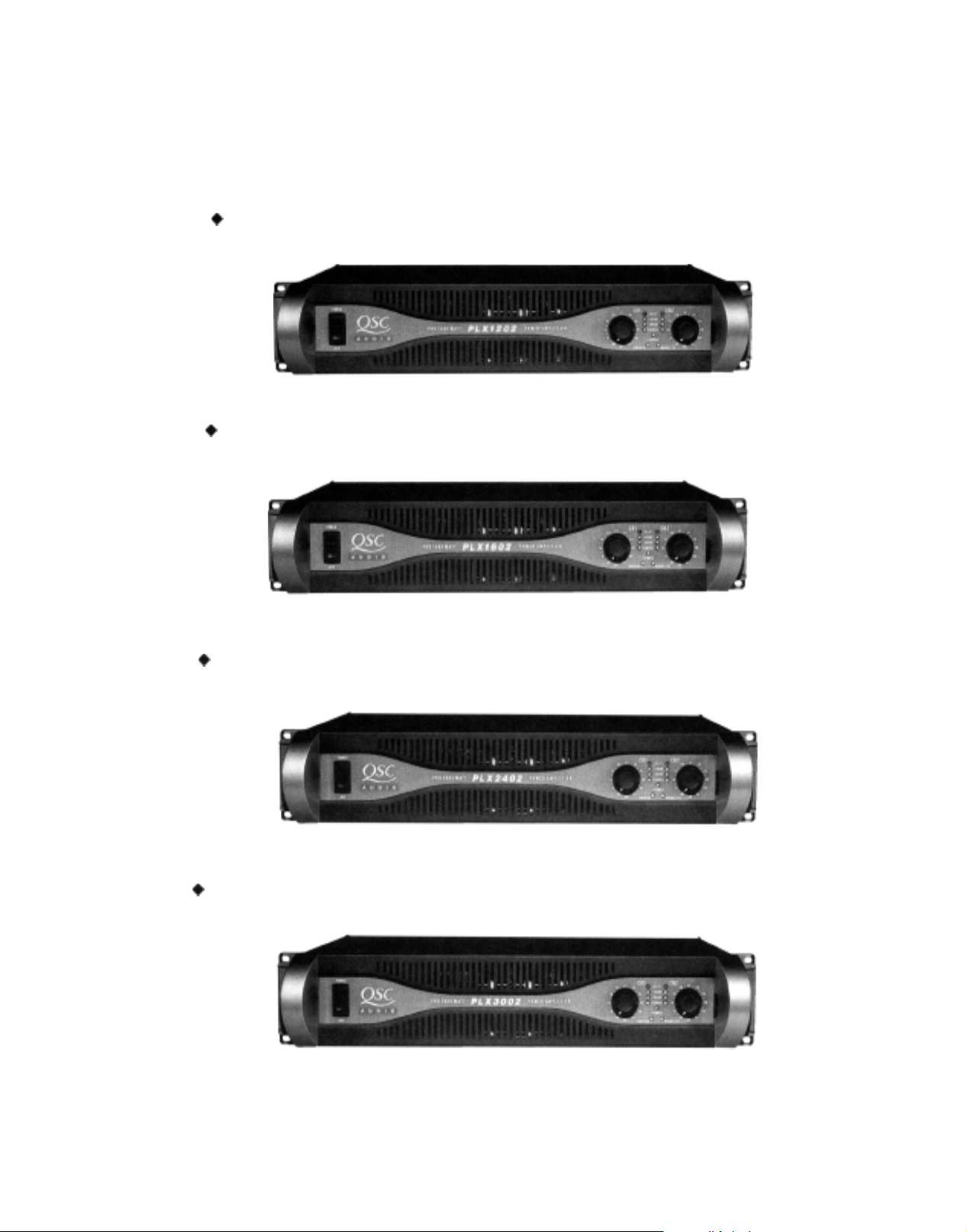
▲ PLX 1202
▲▲
▲▲
▲ PLX 1602
▲▲
▲▲
▲ PLX 2402
▲▲
▲▲
▲ PLX 3002
▲▲
Technical Service Manual
TD-000078-00
TD-000078-00
Page 2
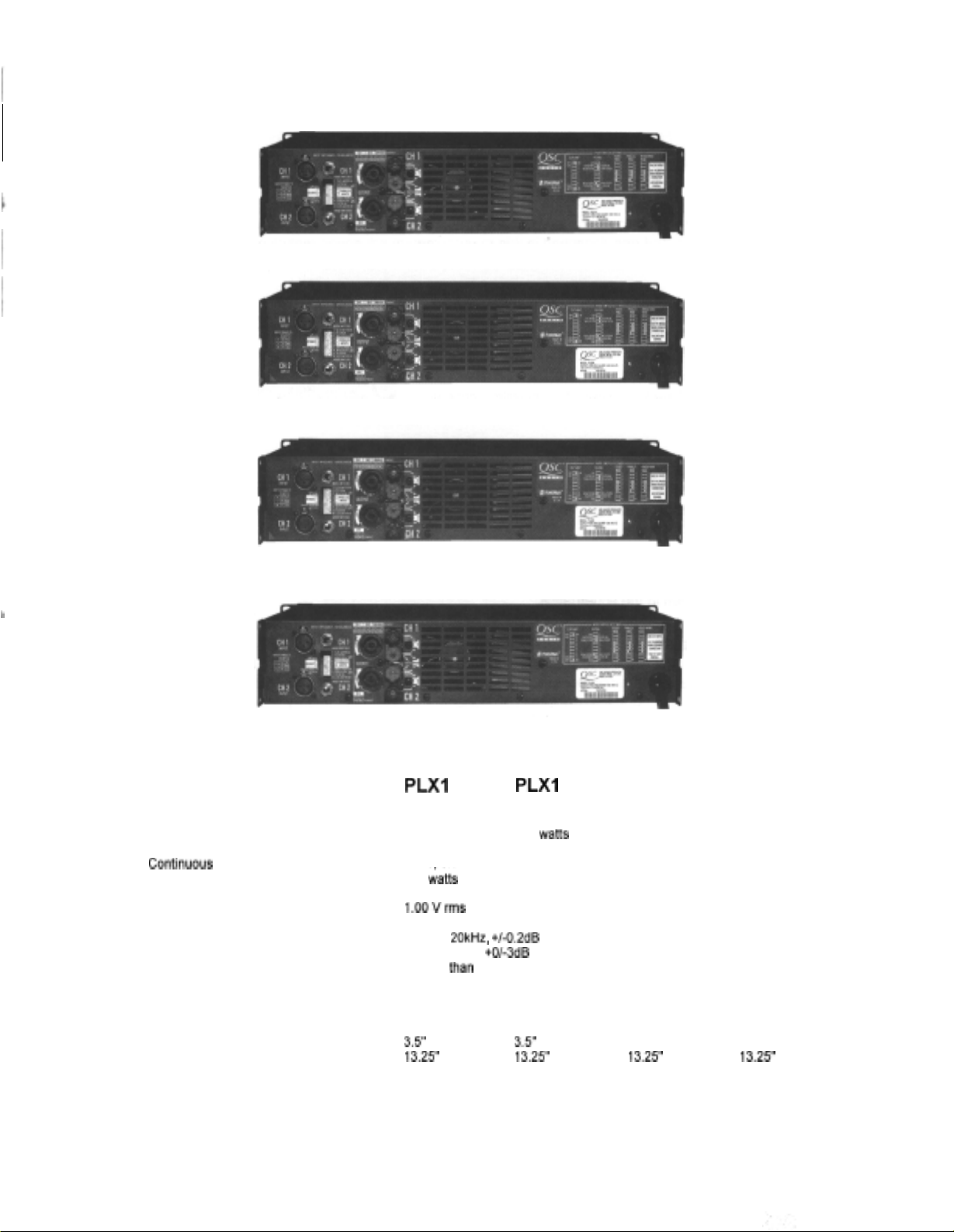
+ PLX
+
PLX 1602
+
PLX 2402
1202
+
PLX 3002
Page 3

PLX SERIES
SERVICE MANUAL
PLX
1202
PLX 1602
PLX 2402
PLX 3002
QSC Technical Services
Wats: I
Local:
Fax: 1-714-754-6173
QSC Technical Support BBS
QSC Audio Products, Inc.
1675 MacArthur Blvd.
Costa Mesa,
-%OO-772-2034
1-714-957-7150
I -714-668-7567
1-800-856-6003
CA
92626
http://www.qscaudio.com
Page 4

Table of Contents
PLX Product Specifications ................................................................
Introduction ........................................................................................
Test and Calibration ............................................................................
Troubleshooting PLX ...........................................................................
PLX Parts List
PLX 1202 PCB Assembly (120V) 23
PLX 1202 PCB Assembly (230V) 25
PLX 1202 Chassis Assembly (120V) 28
PLX 1202 Chassis Assembly (230V) 28
PLX 1602 PCB Assembly (120V) 28
PLX 1602 PCB Assembly (230V) 31
PLX 1602 Chassis Assembly (120V) 34
PLX 1602 Chassis Assembly (230V) 34
PLX 2402 PCB Assembly (120V) 35
PLX 2402 PCB Assembly (230V) 38
PLX 2402 Chassis Assembly (120V) 41
PLX 2402 Chassis Assembly (230V) 41
.....................................................
.....................................................
................................................
................................................
.....................................................
.....................................................
................................................
................................................
.....................................................
.....................................................
................................................
................................................
1
2
3
13
PLX 3002 PCB Assembly (120V) 42
PLX 3002 PCB Assembly (230V) 45
PLX 3002 Chassis Assembly (120V) 48
PLX 3002 Chassis Assembly (230V) 49
.....................................................
.....................................................
................................................
................................................
PLX Semiconductors ..............................................................................
Chassis Drawings ...................................................................................
Schematics
PLX 1202 Main PCB Schematics 57
PLX 1602 Main PCB Schematics 62
PLX 2402 Main PCB Schematics 67
PLX 3002 Main PCB Schematics 72
.....................................................
.....................................................
.....................................................
.....................................................
PLX Series PCB Circut Board Drawings .................................................
50
53
73
Page 5
PLX
1202
PLX 1602
PLX 2402
PLX Product Specifications
PLX
3002
Output
Power (per channel):
Continuous Average
8
ohms,
ohms,
Impedance
2OHz-2OkHz,
2OHz-2OkHz,
Average
2OHz - 2OkHz,
4
Con0nuous
8 ohms,
Voltage Gain (dB)
Sensitivity (for rated power @ 8 ohms)
Distortion
Frequency Response (LF Switched Off)
Damping Factor (1
Noise
Input
Dimensions
Faceplate Width
Faceplate Height
Chassis Depth
Weight
Net, Lbs/kg
Output
Power both channels driven:
0.03%
THD
0.05%
Output
kHz
THD
Power bridged mono
0.1% THD
and Below)
PLXI
PLXI
202
200watts
325
watts
ooeration:
700
iatts
32
1.00vrms
SMPTE-IM
2OHz to 2OkHz,
8Hz to 5OkHz, +Ol-3dB
Greater
106dB
6k unbalanced,
Standard 19” Rack Mounting
3.Y
13.2Y
2119.5 2119.5
Less
than
+I-0.2dB
than
500
below rated output (20 Hz to 20 kHz)
12k
balanced
602
300
waKs
500
watts
1100
watts 1500 watts
32
1.20 Vrms
0.01%
3.r
13.2v
PLX2402
425watts 550
700
watts 900watts
32
1.50 Vrms
3.5” 3.Y
13.2Y 13.2Y
2119.5
PLX3002
2000 watts
32
1.70
2119.5
watts
vrms
Page 6
Introduction
This manual is prepared to assist service personnel with the repair and calibration of PLX power
amplifiers
and sophisticated audio test equipment.
Documentation
This manual contains schematics, printed circuit board (PCB) drawings, parts lists, and
mechanical assembly drawings. This information should be used in conjunction with the
test and troubleshooting guide.
The electrical and electronic components are identified by circuit identification numbers on
the schematics and the parts list. The test
designations shown in the schematics.
.
The procedures described in this manual require advanced technical experience
CAUTION: To reduce the risk of electric shock,
do not remove the cover. No user-serviceable
parts inside. Refer servicing to qualified
personnel.
WARNING: To prevent fire or electric shock, do
not expose this equipment to rain or moisture.
&
troubleshooting sections refer to
CAUTION
Equivalent Parts
Although many of the electronic components used in this product may be available from
WC.
electronic suppliers, some components are specially tested and approved by
product repaired with
Repairs performed using non-QSC parts may void the product warranty.
you may contact
Parts orders to QSC should include the product model number, the part description, and
the QSC part number (from the parts list in this manual). Parts will be shipped via UPS,
F.O.B. Costa Mesa, California. Shipping, handling and COD charges may be added to
the cost of the parts.
non-WC
QSC
Technical Services for assistance.
supplied components may not meet factory specifications.
men
A
in doubt,
Factory Repair
It may become necessary to return a product to the factory for repair. Call QSC Technical
Services for return instructions. QSC Technical Services may be reached at (800)
772-2834.
Test and Troubleshooting Equipment
-Audio
-
Distortion Analyzer capable of 0.01% THD+N
-
High Power Load Bank
-
Function Generator 8 Digital Multimeter
-
2OMHz
Oscilloscope
-
Variac (0-140
VAC, 30-40A)
(8,4,8
2
ohms)
Precision - System One
+
Thermometer
2
Page 7

Test & Calibration
PLX 1202 Test Procedure
.
SET-UP
1.
Connect a test load to the output terminals of the amplifier.
-
2. Make sure Mode Switches 1
3. Connect a distortion analyzer with a resolution of
output terminals of the amplifier. Enable the
4. Connect a dual-channel oscilloscope to the following test points:
Chl
-
a
IOX
(vertical sensitivity -
Ch2
-
a IX scope probe (vertical sensitivity -
output.
5.
Set amp gain pots fully clockwise and turn on power switch.
6. Connect the output of the signal generator to the input terminals of the amplifier and
select an output of 1.30
7. Plug the amplifier into a variac and set up an AC line current monitor.
. POWER UP 8 MUTE DELAY TEST
CAUTION: To avoid damage to the main printed circuit board, place a 50 ohm
240VAC) in series with the high
supply has a shorted device at initial power up, this AC resistor pad will help prevent undue damage. After
the amplifier has been fully powered up via the variac, confirm that the amplifier has achieved
stable operation during idle. Remove AC power from the amplifier and disconnect the series
resistor for normal operation. Continue with the test
10 are in the default position (1 on, 10 on, all others off).
O.Ol%, 20-2OkHz
8OkHz
low pass filter.
2V/cm)
scope probe to the channel speaker output.
O.lV/cm)
VRMS,
1
kHz
sine wave.
(+)
lead on the AC cable during variac ramp up. If the switching power
&
calibration process.
to the distortion analyzer
(or better) to the
225W
resistor (100 ohm,
I. Slowly raise the variac voltage and watch for excessive current draw (line current
greater than
0.5A
a.c. at 60 Volts). This is slightly less for 240V.
Pause at
(2OOVAC European) for three seconds until the mute I protect circuit disengages.
Continue to
12OVAC
(240V European).
2. Verify that the fan is operating at low speed.
3. Turn the power switch off and on a few times to verify the 3 second power-up muting
delay.
l CHANNEL OUTPUT
I. Look for amplified signal on the scope for channel 1. Switch the input signal and scope
/
to channel 2 and repeat output test. Check for noisy
contaminated gain pots by
observing general instability on the distortion waveform while adjusting the gain control
levels.
2. Select an 8 ohm load and confirm that this amplifier is producing 200 watts at 1 kHz just
below the point of clipping. Check both channels.
l BRIDGE MODE
1. Turn the power switch off.
#7
2. Set Mode Switch
on CH2 are disabled with Mode Switch
3.
Set load to both red output binding posts
4. Apply a 1.30
in the on position. The gain control, limiter, and filter switch positions
#7
on.
(CHI
positive and CH2 negative).
VRMS,
1
kHz
sinewave input to channel I of the amplifier. Check the power
and verify that the output does not immediately collapse. Check for 700 watts at 8 ohms.
9OVAC
Page 8

5.
Turn power off and place the amplifier back into the Stereo mode with output
loads connected to each channel.
. BIAS
1. Let the amplifier cool down to room temperature.
2. With an input amplitude of
1.3OVrms
input signal 20dB (80%) from full output. Adjust the crossover
VR166 (CH2) for about a
4OOmVpk-pk
increase the input frequency to
trimpot
2OkHz.
VR43
crossover spike protruding from the noise trace
on the oscilloscope. It will be necessary to have the oscilloscope measure unfiltered
distortion from the amplifier in order to see the crossover spike. It is necessary to
disable the 80kHz
lowpass
filter on the analyzer for this test.
Further trim so that
the total distortion for that channel is less than 0.1% THD+N.
3. With the trim settings achieved, and with no signal plugged into the amplifier and with an
8 ohm load, verify that the AC idle current from the AC service is no more than 1 .O
amperes.
4. Let the amplifier cool down and check channel 2.
. SHORT CIRCUIT CURRENT
1.
Select a 2 ohm load and apply a
of the amplifier.
Ensure that power is on and that the gain controls are fully up.
1.3Vrms
sinewave (1
kHz)
input signal to both channels
2. While the amplifier is producing power into the loads, apply a short to the output binding
posts of each channel. In other words, apply a jumper between the red and black
binding posts of each channel. Once this is done, combined AC line current draw for
both channels should be no greater than
13A ac.
This is with a 120 volt AC service to
the amplifier. Current may be lower if AC line voltage is lower.
3. Remove the short from each channel and verify that the channels recover in to 2 ohm
loads. The output should not experience any hang up and a full
sinewave
should be
present just as it was before a short was applied for this test.
4. If the amplifier does not pass any of the above steps, troubleshoot the current limit
section of the amplifier. If steps 2, 3, and 4 above pass, continue to the next test
FREQUENCY RESPONSE.
Reduce the
(CHl)
and
l FREQUENCY RESPONSE
1,
Set load to 8 ohms and scale the input generator to gain 1 watt of power from the
amplifier on each channel. Gain controls on the amplifier should be fully up.
2.
Check frequency response from
2OHz
to 20kHz
(+I- 0.2OdB)
by sweeping random
frequencies between these extremes. This is done by verifying the same voltage
amplitude at each of the frequencies selected (within
2OHz
to
2OkHz).
Check both
channels.
l POWER vs. DISTORTION TEST
I. Check to ensure that both channels will produce rated power at
2OHz, 2KHz,
into an 8 ohm load.
2. While verifying rated power, check that at all frequencies the distortion measurement is
less than or equal to 0.03% THD.
l THERMAL TEST
1. Set input frequency to 1 KHz and short both channels while they are producing power into
a load.
2. Apply a short to the output of each channel.
3. AC line current draw should be about 11 - 13.5 amperes for both channels. As the
amplifier gets hot, there will be some current drift upwards and the fan speed will
increase. This is not a problem as long as the case temperature on the output
transistors does not exceed
105
degrees C.
and 20kHz.
4
Page 9
4.
Verify that the NTC circuit causes thermal shutdown after an extended period.
5. When thermal shutdown occurs, verify AC idle current of less that 0.90 amperes
l CM TEST
1. Select an 8 ohm load and confirm that this amplifier is producing rated power.
2. Check the Common Mode of the amplifier by inserting a
channel and observe about 6
dB
of output voltage reduction. There will also be a 180
1/4”
input jack halfway into each
degree phase inversion at the output of the channel under test.
l OUTPUT NOISE
1. Set the amplifier gain controls all the way up, with a 1
kHz 1.3OVrms sinewave
signal. Note the output level at full power just below clipping. Adjust gain if needed.
2. Remove the input signal connector from the amplifier and measure the residual noise
level produced into the load by the amplifier. The noise signal should be 107
from the full output power point measured. A signal to noise ratio should be better than
or equal to
l FINAL CHECK
107dB.
Check both channels.
This completes the amplifier test procedure for this model.Inspect the amplifier for
mechanical defects. Inspect the solder connections. Reassemble the amplifier and verify
the amplifier’s operation before returning the product to service.
input
dB
down
PLX 1602 Test Procedure
.
SET-UP
1.
Connect a test load to the output terminals of the amplifier.
2.
Make sure Mode Switches 1
Connect a distortion analyzer with a resolution of
3.
output terminals of the amplifier.Enable the 80kHz low pass filter.
4.
Connect a dual-channel oscilloscope to the following test points:
Chl -
a 1 OX (vertical sensitivity -
Ch2
-
a IX scope probe (vertical sensitivity -
output.
5.
Set amp gain pots fully clockwise and turn on power switch.
Connect the output of the signal generator to the input terminals of the amplifier and
6.
select an output of 1.30
Plug the amplifier into a variac and set up an AC line current monitor.
7.
l POWER UP 8 MUTE DELAY TEST
CAUTION: To avoid damage to the main printed circuit board, place a 50 ohm 225W resistor (100 ohm,
240VAC) in series with the high
supply has a shorted device at initial power up, this AC resistor pad will help prevent undue damage. After
the amplifier has been fully powered up via the variac, confirm that the amplifier has achieved
stable operation during idle. Remove AC power from the amplifier and disconnect the series
resistor for normal operation. Continue with the test
Slowly raise the variac voltage and watch for excessive current draw (line current
greater than
(2OOVAC
European) for three seconds until the mute I protect circuit disengages.
Continue to
0.5A a.c
12OVAC (24OV
at 60 Volts).
Verify that the fan is operating at low speed.
-
10 are in the default position (1 on, 10 on, all others off)
VRMS,
1
(+)
lead on the AC cable during variac ramp up. If the switching power
European).
O.Ol%, 20-20kHz
2V/cm)
scope probe to the channel speaker output.
O.lV/cm)
kHz
sine wave.
&
calibration process.
T/I;s is s/;ghf/y less
to the distortion analyzer
for 240V. Pause at
(or better) to the
9OVAC
Page 10

3. Turn the power switch off and on a few times to verify the 3 second power-up muting
delay.
. CHANNEL OUTPUT
1. Look for amplified signal on the scope for channel 1. Switch the input signal and scope
to channel 2 and repeat output test. Check for noisy
/
contaminated gain pots by
observing general instability on the distortion waveform while adjusting the gain control
levels.
2. Select an 8 ohm load and confirm that this amplifier is producing 300 watts at 1 kHz just
below the point of clipping. Check both channels.
. BRIDGE MODE
1. Turn the power switch off.
2. Set Mode Switch
on CH2 are disabled with Mode Switch
3. Set load to both red output binding posts
4. Apply a 1.30
#7
in the on position. The gain control, limiter, and filter switch positions
#7
on.
(CHI
positive and CH2 negative).
VRMS,
1
kHz
sinewave input to channel 1 of the amplifier. Check the power
and verify that the output does not immediately collapse. Check for 1000 watts at 8
ohms.
5.
Turn power off and place the amplifier under test back into the Stereo mode with output
loads connected to each channel.
l BIAS
I. Let the amplifier cool down to room temperature.
2. With an input amplitude of
input signal 20dB (80%) from full output. Adjust the crossover
VR166 (CH2) for about a
1.3OVrms
increase the input frequency to 20kHz. Reduce the
4OOmVpk-pk
trimpot
VR43
crossover spike protruding from the noise trace
on the oscilloscope. It will be necessary to have the oscilloscope measure unfiltered
distortion from the amplifier in order to see the crossover spike.
disable the 80kHz
lowpass
filter on the analyzer for this test. Further trim so that
It is necessary to
the total distortion for that channel is less than 0.1% THD+N.
3. With the trim settings achieved, and with no signal plugged into the amplifier and with an
8 ohm load, verify that the AC idle current from the AC service is no more than 1 .O
amperes.
4. Let the amplifier cool down and check channel 2.
(CHl)
and
l SHORT CIRCUIT CURRENT
1.
Select a 2 ohm load and apply a
of the amplifier.Ensure that power is on and that the gain controls are fully up.
2. While the amplifier is producing power into the loads, apply a short to the output binding
posts of each channel.
binding posts of each channel. Once this is done, combined AC line current draw for
both channels should be no greater than
the amplifier. Current may be lower if AC line voltage is lower.
3. Remove the short from each channel and verify that the channels recover in to 2 ohm
loads. The output should not experience any hang up and a full
present just as it was before a short was applied for this test.
4. If the amplifier does not pass any of the above steps, troubleshoot the current limit
section of the amplifier. If steps 2, 3, and 4 above pass, continue to the next test
FREQUENCY RESPONSE.
6
1.3Vrms
sinewave (1
kHz)
input signal to both channels
In other words, apply a jumper between the red and black
13A
ac. This is with a 120 volt AC service to
sinewave
should be
Page 11

l FREQUENCY RESPONSE
I.
Set load to 8 ohms and scale the input generator to gain 1 watt of power from the
amplifier on each channel. Gain controls on the amplifier should be fully up.
2. Check frequency response from
2OHz
to 20kHz
(+I- 0.2OdB)
by sweeping random
frequencies between these extremes. This is done by verifying the same voltage
2OHz
amplitude at each of the frequencies selected (within
to 20kHz). Check both
channels.
l POWER vs. DISTORTION TEST
1. Check to ensure that both channels will produce rated power at
2OHz, 2KHz,
into an 8 ohm load.
2.
While verifying rated power, check that at all frequencies the distortion measurement is
less than or equal to 0.03% THD.
l THERMAL TEST
1.
Set input frequency to 1 KHz and short both channels while they are producing power into
a load.
2. Apply a short to the output of each channel.
3. AC line current draw should be about
II -
13.5 amperes for both channels. As the
amplifier gets hot, there will be some current drift upwards and the fan speed will
increase. This is not a problem as long as the case temperature on the output
transistors does not exceed 105 degrees
C.
4. Verify that the NTC circuit causes thermal shutdown after an extended period.
5. When thermal shutdown occurs, verify AC idle current of less that 0.90 amperes.
and 20kHz.
l CM TEST
1. Select an 8 ohm load and confirm that this amplifier is producing rated power.
2. Check the Common Mode of the amplifier by inserting a
dB
channel and observe about 6
of output voltage reduction. There will also be a 180
1/4”
input jack halfway into each
degree phase inversion at the output of the channel under test.
l OUTPUT NOISE
I. Set the amplifier gain controls all the way up, with a 1
signal.
Note the output level at full power just below clipping. Adjust gain if needed.
kHz 1.3OVrms sinewave
2. Remove the input signal connector from the amplifier and measure the residual noise
level produced into the load by the amplifier. The noise signal should be 107
from the full output power point measured. A signal to noise ratio should be better than
107dB.
or equal to
l FINAL CHECK
This completes the amplifier test procedure for this model.
Check both channels.
Inspect the amplifier for
mechanical defects. inspect the solder connections. Reassemble the amplifier and
the amplifier’s operation before returning the product to service.
PLX 2402 Test Procedure
l SET-UP
1. Connect a test load to the output terminals of the amplifier.
2. Make sure Mode Switches 1
- 10
are in the default position (1 on, 10 on, all others off).
input
dB
down
veri@
Page 12

3. Connect a distortion analyzer with a resolution of
O.Ol%, 20-20kHz
(or better) to the
output terminals of the amplifier. Enable the 80kHz low pass filter.
4. Connect a dual-channel oscilloscope to the following test points:
Chl
-
a
1OX
(vertical sensitivity - 2V/cm) scope probe to the channel speaker output.
Ch2
-
a IX scope probe (vertical sensitivity - 0.
IV/cm)
to the distortion analyzer
output.
5. Set amp gain pots fully clockwise and turn on power switch.
6. Connect the output of the signal generator to the input terminals of the amplifier and
select an output of 1.50
VRMS
1
kHz
sine wave.
7. Plug the amplifier into a variac and set up an AC line current monitor.
l POWER UP
&
MUTE DELAY TEST
CAUTION: To avoid damage to the main printed circuit board, place a 50 ohm
240VAC) in series with the high
supply has a shorted device at initial power up, this AC resistor pad will help prevent undue damage. After
the amplifier has been fully powered up via the variac, confirm that the amplifier has achieved
stable operation during idle. Remove AC power from the amplifier and disconnect the series
resistor for normal operation. Continue with the test
(+)
lead on the AC cable during variac ramp up. if the switching power
&
calibration process.
225W
resistor (100 ohm,
1. Slowly raise the variac voltage and watch for excessive current draw (line current
greater than
(2OOVAC
European) for three seconds until the mute / protect circuit disengages.
Continue to
0.5A a.c
at 60 Volts).
12OVAC (24OV
This
European).
is
slight/y /ess fof
24OV.
Pause at
2. Verify that the fan is operating at low speed.
3.
Turn the power switch off and on a few times to verify the 3 second power-up muting
delay.
l CHANNEL OUTPUT
I. Look for amplified signal on the scope for channel
to channel 2 and repeat output test. Check for noisy
1.
Switch the input signal and scope
/
contaminated gain pots by
observing general instability on the distortion waveform while adjusting the gain control
levels.
2. Select an 8 ohm load and confirm that this amplifier is producing 425 watts at 1 kHz just
below the point of clipping. Check both channels.
l BRIDGE MODE
1. Turn the power switch off.
2. Set Mode Switch
on CH2 are disabled with Mode Switch
3. Set load to both red output binding posts
4. Apply a 1.30
#7
in the on position. The gain control, limiter, and filter switch positions
#7
on.
(CHI
positive and CH2 negative).
VRMS,
1
kHz sinewave
input to channel 1 of the amplifier. Check the power
and verify that the output does not immediately collapse. Check for 1500 watts at 8
ohms.
5. Turn power off and place the amplifier under test back into the Stereo mode with output
loads connected to each channel.
l BIAS
1.
Let the amplifier cool down to room temperature.
2. With an input amplitude of
input signal 20dB (80%) from full output. Adjust the crossover
VR166 (CH2) for about a
1.5OVrms,
increase the input frequency to
4OOmVpk-pk
2OkHz.
trimpot
VR43
crossover spike protruding from the noise trace
on the oscilloscope. It will be necessary to have the oscilloscope measure unfiltered
distortion from the amplifier in order to see the crossover spike.
It is necessary to
9OVAC
Reduce the
(CHl)
and
Page 13

disable the 80kHz
the total distortion for that channel is less than 0.1%
lowpass
filter on the analyzer for this test.Further trim so that
THD+N,
3. With the trim settings achieved, and with no signal plugged into the amplifier and with an
8 ohm load, verify that the AC idle current from the AC service is no more than 1 .O
amperes.
4. Let the amplifier cool down and check channel
l SHORT CIRCUIT CURRENT
1.
Select a 2 ohm load and apply a
1.3Vrms
2.
sinewave (1
kHz)
input signal to both channels
of the amplifier.Ensure that power is on and that the gain controls are fully up.
2. While the amplifier is producing power into the loads, apply a short to the output binding
posts of each channel. In other words, apply a jumper between the red and black
binding posts of each channel. Once this is done, combined AC line current draw for
both channels should be no greater than
13A
ac. This is with a 120 volt AC service to
the amplifier. Current may be lower if AC line voltage is lower.
3. Remove the short from each channel and verify that the channels recover in to 2 ohm
loads. The output should not experience any hang up and a full
sinewave
should be
present just as it was before a short was applied for this test,
4. If the amplifier does not pass any of the above steps, troubleshoot the current limit
section of the amplifier. If steps 2, 3, and 4 above pass, continue to the next test
FREQUENCY RESPONSE.
l FREQUENCY RESPONSE
1. Set load to 8 ohms and scale the input generator to gain 1 watt of power from the
amplifier on each channel. Gain controls on the amplifier should be fully up.
2. Check frequency response from
2OHz
to 20kHz
(+/- 0.2OdB)
by sweeping random
frequencies between these extremes. This is done by verifying the same voltage
amplitude at each of the frequencies selected (within
2OHz
to 20kHz). Check both
channels.
l POWER vs. DISTORTION TEST
1. Check to ensure that both channels will produce rated power at
2OHz, 2KHz,
into an 8 ohm load.
2. While verifying rated power, check that at all frequencies the distortion measurement is
less than or equal to 0.03%
l THERMAL TEST
THD.
1. Set input frequency to 1 KHz and short both channels while they are producing power into
a load.
2. Apply a short to the output of each channel.
11
-
3. AC line current draw should be about
13.5 amperes for both channels. As the
amplifier gets hot, there will be some current drift upwards and the fan speed will
increase, This is not a problem as long as the case temperature on the output
transistors does not exceed 105 degrees C.
4. Verify that the NTC circuit causes thermal shutdown after an extended period.
5,
When thermal shutdown occurs, verify AC idle current of less that 0.90 amperes.
l CM TEST
I. Select an 8 ohm load and confirm that this amplifier is producing rated power.
2. Check the Common Mode of the amplifier by inserting a
114”
input jack halfway into each
channel and observe about 6 dB of output voltage reduction. There will also be a 180
degree phase inversion at the output of the channel under test.
and 20kHz.
9
Page 14

l OUTPUT NOISE
1. Set the amplifier gain controls all the way up, with a I
signal.
Note the output level at full power just below clipping. Adjust gain if needed.
kHz 1.5OVrms sinewave
2. Remove the input signal connector from the amplifier and measure the residual noise
level produced into the load by the amplifier. The noise signal should be 107
from the full output power point measured. A signal to noise ratio should be better than
or equal to
l FINAL CHECK
107dB.
Check both channels.
This completes the amplifier test procedure for this model.Inspect the amplifier for
mechanical defects. Inspect the solder connections. Reassemble the amplifier and verify
the amplifier’s operation before returning the product to service,
PLX 3002 Test Procedure
l SET-UP
1. Connect a test load to the output terminals of the amplifier.
2. Make sure Mode Switches 1 - 10 are in the default position (1 on, 10 on, all others off).
3.
Connect a distortion analyzer with a resolution of
output terminals of the amplifier. Enable the 80kHz low pass filter.
4. Connect a dual-channel oscilloscope to the following test points:
-
a
1OX
Chl
Ch2
(vertical sensitivity -
-
a 1X scope probe (vertical sensitivity -
2V/cm)
scope probe to the channel speaker output.
output.
5.
Set amp gain pots fully clockwise and turn on power switch.
6. Connect the output of the signal generator to the input terminals of the amplifier and
select an output of 1.70
VRMS,
1
kHz
sine wave.
7. Plug the amplifier into a variac and set up an AC line current monitor.
O.Ol%,
O.lV/cm)
20-20kHz
(or better) to the
to the distortion analyzer
input
dB
down
. POWER UP 8 MUTE DELAY TEST
CAUTION: To avoid damage to the main printed circuit board, place a 50 ohm 225W resistor (100 ohm,
240VAC) in series with the high
supply has a shorted device at initial power up, this AC resistor pad will help prevent undue damage. After
the amplifier has been fully powered up via the variac, confirm that the amplifier has achieved
stable operation during idle. Remove AC power from the amplifier and disconnect the series
resistor for normal operation. Continue with the test
1.
Slowly raise the variac voltage and watch for excessive current draw (line current
greater than
(2UOVAC
Continue to
0.5A
a.c. at 60 Volts).
European) for three seconds until the mute / protect circuit disengages.
12OVAC
(+)
lead on the AC cable during variac ramp up. If the switching power
TIG.s is s/ight/y
(240V European).,
&
calibration process.
less for
24UV.
Pause at
2. Verify that the fan is operating at low speed.
3. Turn the power switch off and on a few times to verify the 3 second power-up muting
delay.
l CHANNEL OUTPUT
1.
Look for amplified signal on the scope for channel 1. Switch the input signal and scope
to channel 2 and repeat output test. Check for noisy I contaminated gain pots by
observing general instability on the distortion waveform while adjusting the gain control
levels.
9OVAC
10
Page 15

2. Select an 8 ohm load and confirm that this amplifier is producing
550
watts at 1 kHz just
below the point of clipping. Check both channels.
l BRIDGE MODE
1. Turn the power switch off.
2. Set Mode Switch
on CH2 are disabled with Mode Switch
3. Set load to both red output binding posts
4. Apply a 1.30
#7
in the on position. The gain control, limiter, and filter switch positions
#
7 on.
(CHI
positive and CH2 negative).
VRMS,
1
kHz
sinewave input to channel 1 of the amplifier. Check the power
and verify that the output does not immediately collapse. Check for 2000 watts at 8
ohms.
5. Turn power off and place the amplifier under test back into the Stereo mode with output
loads connected to each channel.
l BIAS
1.
Let the amplifier cool down to room temperature.
2. With an input amplitude of
input signal 20dB
VRl66
(CH2) for about a
(80°h)
1.7OVrms
increase the input frequency to 20kHz. Reduce the
from full output. Adjust the crossover
4OOmVpk-pk
crossover spike protruding from the noise trace
trimpot
VR43
on the oscilloscope. It will be necessary to have the oscilloscope measure unfiltered
distortion from the amplifier in order to see the crossover spike. It is necessary to
disable the 80kHz
lowpass
filter on the analyzer for this test.Further trim so that
the total distortion for that channel is less than 0.1% THD+N.
3,
With the trim settings achieved, and with no signal plugged into the amplifier and with an
8 ohm load, verify that the AC idle current from the AC service is no more than 1 .O
amperes.
4. Let the amplifier cool down and check channel
2.
(CHI)
and
l SHORT CIRCUIT CURRENT
1.
Select a 2 ohm load and apply a
1.3Vrms
sinewave (1
kHz)
input signal to both channels
of the amplifier.Ensure that power is on and that the gain controls are fully up.
2,
While the amplifier is producing power into the loads, apply a short to the output binding
posts of each channel. In other words, apply a jumper between the red and black
binding posts of each channel. Once this is done, combined AC line current draw for
both channels should be no greater than
13A
ac. This is with a 120 volt AC service to
the amplifier. Current may be lower if AC line voltage is lower.
3. Remove the short from each channel and verify that the channels recover in to 2 ohm
loads. The output should not experience any hang up and a full
sinewave
present just as it was before a short was applied for this test.
4. If the amplifier does not pass any of the above steps, troubleshoot the current limit
section of the amplifier. If steps 2, 3, and 4 above pass, continue to the next test
FREQUENCY RESPONSE.
l FREQUENCY RESPONSE
1. Set load to 8 ohms and scale the input generator to gain I watt of power from the
amplifier on each channel. Gain controlson the amplifier should be fully up.
2. Check frequency response from
to 20kHz
(+I- 0.2OdB)
by sweeping random
2OHz
frequencies between these extremes. This is done by verifying the same voltage
amplitude at each of the frequencies selected (within
2OHz
to 20kHz). Check both
channels.
should be
11
Page 16

l POWER vs. DISTORTION TEST
1.
Check to ensure that both channels will produce rated power at
2OH2, 2KHz,
into an 8 ohm load.
2. While verifying rated power, check that at all frequencies the distortion measurement is
less than or equal to 0.03% THD.
l THERMAL TEST
I. Set input frequency to
1 KHz and short both channels while they are producing power into
a load.
2. Apply a short to the output of each channel.
3. AC line current draw should be about 11
-
13.5 amperes for both channels. As the
amplifier gets hot, there will be some current drift upwards and the fan speed will
increase. This is not a problem as long as the case temperature on the output
transistors does not exceed 105 degrees
C.
4. Verify that the NTC circuit causes thermal shutdown after an extended period.
5. When thermal shutdown occurs, verify AC idle current of less that 0.90 amperes.
l CM TEST
1. Select an 8 ohm load and confirm that this amplifier is producing rated power.
2. Check the Common Mode of the amplifier by inserting a
channel and observe about 6 dB of output voltage reduction. There
114”
input jack halfway into each
will
also be a 180
degree phase inversion at the output of the channel under test.
l OUTPUT NOISE
1. Set the amplifier gain controls all the way up, with a 1
signal.
Note the output level at full power just below clipping. Adjust gain if needed.
kHz 1.7OVrms sinewave
2. Remove the input signal connector from the amplifier and measure the residual noise
level produced into the load by the amplifier. The noise signal should be 107
from the full output power point measured. A signal to noise ratio should be better than
or equal to
107dB.
Check both channels.
and 20kHz.
input
dB
down
l FINAL CHECK
This completes the amplifier test procedure for this model.
Inspect the amplifier for
mechanical defects. Inspect the solder connections. Reassemble the amplifier and verify
the amplifier’s operation before returning the product to service.
12
Page 17
T r o ubleshooting
PLX 1202 l PLX 1602 l PLX 2402 l PLX 3002
Power Supply -
In order to improve
are driven by an active, direct coupled integrated circuit, rather than a gate drive transformer.
driver failure should be rare (when correctly assembled) but when the
following parts:
CHECKLIST AFTER BLOWN
Q96, Q97,
D78, D79,
Ul8, lR2110
also typically damage the gate coupling parts noted above.
Ul9,
SOMETIMES
RARELY
PROBABLE CAUSES OF MASSIVE
SHORTS IN CONTROL CIRCUIT.
The parts operate well within their ratings and should hold up well in the field. The usual cause of failure is
when both
signal to one part to remain on when the other part is supposed to turn on. Shorts from solder or debris are
one obvious cause.
SHORTS IN THE LOAD.
Although there is peak current shutdown, shorts in the power amplifier transistors or secondary-side supply
components can cause currents to increase too quickly to prevent damage.
(IGBT’s
R358, R359,
high-side gate driver, Fault current when low-side
3525 controller, Blows from currents shorted
Ul3,
IGBT’s
EMI
performance, reduce cost, and increase current capacity, the PLX
generally fail in pairs)
gate drive coupling
Ul4, 556,
which has fairly high supply voltage ratings.
powered from 5V output of 3525, which may fail high when 3525 fails.
turn on at once, shorting Pri-Hi to Pri-Lo. This occurs when something causes the drive
Replacing Blown
-
IGBT’S
IGBT
comonents,
FAULTS
check after removing blown
thru Ul8,
IGBTs.
IGBTs
IGBT
or
IGBT’s
blow, it usually damages the
IGBT’s.
IGBT
shorts to upper rail. Such currents
or possibly by overvoltage on the supply rail
OVERVOLTAGE ON THE BIAS SUPPLY.
If the TOP-210 bias supply fails to operate, no harm occurs, the unit simply does not operate.
However, open circuit (missing part) in several key components can cause the Bias supply voltage to be
much too high, This blows the 2110 and thus the
QUICK TEST OF BIAS SUPPLY.
Ramp the AC voltage up slowly to 25% of regular voltage (30V for
normally, the green “power” LED should come on between 30 and
start-up level. If the LED comes on at
until you have measured the bias voltage. The switching will not start until you reach
the
IGBT’s
from blowing.
Confirm that bias voltage at Cl38 is
feedback to U16 and cause overvoltage.
2OV,
18-19V.
IGBT’s.
or not until
Open or missing
5OV,
12OV
unit). If the bias supply is working
35Vz
with its usual, steady
or blinks, DO NOT RAISE VOLTAGE PAST 60V
9OV,
D63,
64, 65, 66, 67 or R349 will break the
“half-brighr
so you can save
13
Page 18
Troubleshooting “TOP-210” Bias Supply.
QUICK TEST OF BIAS SUPPLY.
Ramp the AC voltage up slowly to 25% of regular voltage (30V for
normally, the green “power” LED should come on between 30 and
start-up level.
CAUTION: if the LED comes on at
until you have measured the bias voltage. The switching will not start until you reach
the
IGBT’s
from blowing.
Confirm that bias voltage at Cl38 is
BIAS SUPPLY VOLTAGE MUCH TOO HIGH
D63,64,65,66,67
NO BIAS SUPPLY VOLTAGE
U16 missing or blown.
Tl missing, reversed, or open primary
D62 open or missing.
BIAS VOLTAGE ERRORS
The exact voltage is controlled by the feedback through
Cl38 is the
D63,
Cl39 , is the
D66,
R349 subtracts about
Ul6
uses this feedback to adjust the “on” time at pin 5, in order
charging Cl38 and thus maintain regulation of the
C142,
“hunting”.
Q99
and associated R374 reduce the voltage of the Bias supply by 33% when the AC voltage is turned off.
This prevents the Power LED from showing at half brightness after turn-off, since U16 continues to run
from the main filters for some time after shut down R375 and 376 sense the output of
AC” comparator, and cause
AC is turned on.
“+18V’
64, 65 each subtract a diode drop
a
IOV zener
R356,
or R349 open or missing -- breaks feedback to U16
rail with about
“+16V”
rail with about
diode , plus diode
0.5V,
bringing the net voltage at
and R349 form a closed-loop stability circuit which prevents the regulated voltage from
18.8V
Q99
to turn on. If
2OV,
or not until
18-19V.
typical.
(0.7V)
16.6V typcial.
D67,
subtract about 1 IV from
5OV,
from Cl38.
+16V
Q99
is shorted, the bias voltages will remain 33% low when
or blinks, DO NOT RAISE VOLTAGE PAST 60V
D63, 64_
Ul6,
feedback pin 4, to about
and
12OV
unit). If the bias supply is working
35V,
with its usual, steady
9OV,
65, 66, 67 and R349 as follows:
+16.6V.
5.lV.
toraise
+18V
or lower the
supplies
flyback
Ul3:3,
“half-brighf’
so you can save
voltage
the “Loss of
14
REPLACING BLOWN TOP-210.
If U16 has blown, check T-l for continuity after removing
measure about 15 ohms
Ul6.
Its primary may be open. Pins I-2 It should
Replacing Blown Output Transistors
OUTPUT TRANSISTOR SHORTED
Stmrk
in one device tend to cause the opposing device to blow as
If an output transistor shorts:
Drive transistor will be shorted
CXNne
transistors will short in pairs (Q39 &
The rest will short in fours
IGBT’s
8 their associated components may
(Q26, Q27, Q71,
(Q28, Q29,
Q34 &
Q72)
Q40,
Q36 &
Q35; Q73, Q74, Q79 8, Q80)
fail
well,
Q37, Q84
8
Q85, Q81 8, Q82)
Page 19
CHECK EMITTER AND BASE RESISTORS WHILE DEVICES ARE REMOVED,
Each output transistor has an associatated pair of 0.47 ohm resistors in parallel.
Each BANK of output transistors has a 15 ohm resistor from base to rail (emitter bus).
Audio Outputs, Troubleshooting Current Limit
WEAK CURRENT LIMIT -- PREMATURE CLIPPING.
The usual symptom of weak output current is premature clipping of one or more peaks of the audio voltage.
This could be caused by missing step, weak current limit, or dead output section.
PREMATURE CLIPPING at 60% VOLTAGE, SIMILAR AT ALL IMPEDANCES:
This points to a step problem (2402, 3002 only). See Step Troubleshooting.
If the amplifier reaches full voltage at 8 ohms, but prematurely clips at 4 ohms or 2 ohms, we can assume
the step is OK but the output current is too low (see below).
NO OUTPUT AT ALL ON ONE POLARITY.
This indicates complete failure (open circuit) in the circuit leading to the dead output polarity. Check the
series components in the current splitter for missing or open:
Ch 1:
Ch 2:
CONSTANT, PREMATURE CLIPPING, WORSE AT LOW IMPEDANCES.
First, check the clamping voltages on
table below. At idle, all four voltages should all be similar. If one is out, check parts according to the
following table
Positive,
Positive,
Ql9, R381, Q20, R70, DIO,
Q64, R383, Q65, Rl93, D35,
C21
(Ch
D14. Negative:
D39. Negative:
I+),
C22 (Ch I-),
Q22, R382, Q21, R71,
Q67, R384, Q66, Rl94, D36,
C56
(Ch
2+), C57
(Ch
Dl I, D12
2-),
as shown in
D37
CLAMPING VOLTAGES ARE WRONG AT IDLE
I+
CHANNEL-POLARITY
Measure voltage on:
3002 and 2402, about
1602, about
1202 about
Voltage too high: missing resistor:
Voltage
Voltage
Voltage wrong: wrong value
The exact voltage varies with temperature. Look for the mismatching value on the weak cell.
A too-low voltage causes early clamping of that output section, as explained in the previous several pages.
If the voltage is correct and current is still low, also check for missing - unsoldered output device, or emitter
resistors.
4,6V,
4.9V.
or missing transistor:
0-0.3V:
or missing resistor
0.7V,
missing resistor:
6V.
shorted transistor
CH
c21
R60
Q14
Ql4,24
R
51,
72
R59
R59,60
CH
l-
c22
R61
Ql5
Ql5,
25
R53,
75
R62
R62,61
2+
CH
C56
RI83
Q59
Q59,69
Rl74,
RI82
Rl82,
195
183
2-
CH
c57
RI84
Q60
Q60,70
Rl76,
198
RI85
Rl85,184
15
Page 20
Audio Power Stage, Current Limit Troubleshooting
CURRENT LIMITS WHICH COLLAPSE PREMATURELY.
An immediate collapse of ALL current limits at full power could be premature triggering of “Power Supply
Cutback”, which is described in the section below. Cutback after several seconds of full power operation at
two ohms is normal.
Cutback of one or more output sections, at full temperature, while approaching full power into two ohms is
also normal. However, cutbacks at 4 ohms, or when cold into two ohms, indicate problems with the
transistor power measuring circuitry.
CLAMPING VOLTAGES COLLAPSE TOO SOON.
CH
CHANNEL-POLARITY
Measure voltage on:
Cuts back too easily: low value,
or high value: R 51,
or missing diode:
CLAMPING VOLTAGES ARE CORRECT, CURRENT STILL WEAK.
Shorted diode
Missing-unsoldered output device or emitter resistor.
TROUBLESHOOTING “POWER SUPPLY CUTBACK”.
As noted in the section on Power Supply, the amplifier’s current limit cuts back when necessary to protect
the power supply. Because the Observed effect is a reduced output voltage, in response to prolonged
operation above the long-term current limit, we commonly refer to this behavior as “power supply cutback”,
but we must remember that it is actually
from the power supply. Full power operation into 2 ohms (both channels) should produce a 50% cutback of
current after several seconds.
If both channels of the amplifier fail to cut back after about 3 seconds, 2-ohms, both channels driven, the
cutback signal is probably missing. CAUTION: Prolonged operation under these conditions could blow
IGBT
or burn out
Check the output (secondary side) pins of U17 (sh 4). Confirm presence of
normally be at about
If
Ul7-pin
4 does not go high, check U17 itself. If it appears OK, trace the circuitry driving U17 (PRIMARY
SIDE, CAUTION). Check for continuity through
R347,
all of which drive optocoupler U17. A short in R346 or Cl31 will also prevent drive to U17.
If
Ul7-pin
4 goes high on schedule, and BOTH channels fail to cut back, trace voltage on
R273 (sh
(sh 2). If only ONE channel fails to cut back, look for missing
(sh 2).
Cl31 controls the speed of cutback.. If missing, the amplifier current limits will enter cutback almost
immediately at or above full power, 4 ohms.
Cl44.
Test for 6-10 seconds maximum.
OV,
and go high (I-5V) after 3 seconds at full power,
3),
which connects to “MUTE+” bus. Continue tracing voltage on MUTE+ to
I+
c21
R67,
73
72
D9
DIO, 14
amp/Tier
CH
l-
c22
R68,
74
R53,
75
D8
Dll,
12
current
L6:2
hmifhg
in response to an overload signal sent
to Pri-Lo, check missing or open
Ql6,
CH
2+
C56
Rl90,
Rl74,
D34
D35,
39
+6V
R 65,
Ql7
CH
2-
c57
196
195
on pin 5. Pin 4 should
(sh I) or
Rl91,
197
Rl76,
198
D33
D36,
37
R343, D61, Q95,
“PS_OL”
Ql6
(sh I) and
Q61, Rl88, Q62
bus to
Q61
16
SHORT CIRCUIT CURRENT DOESN’T CUT BACK.
CAUTION: DO NOT MAINTAIN A SHORTED LOAD IF CUTBACK FAILS TO OCCUR WITHIN 1 SECOND.
It will be necessary to measure the output current with a DC current probe, or by noting the voltage across
a low value resistance with a DC scope, in order to determine which output cell is failing to cut back.
Failure to cut back could indicate either lack of clamping, or lack of voltage cutback. Measure the voltage
on the respective clamp capacitor. If the voltage decreases, but current limiting does not cut back, check
the clamping transistor.
:
Page 21
CLAMPING VOLTAGE DECREASES, BUT NO CURRENT CUTBACK
CHANNEL-POLARITY CH
Measure voltage on:
Check clamp transistor
If the measured voltage on the clamp capacitor is not decreasing to about 50% during the short, check the
circuitry which measures the current during short circuit,
CLAMPING VOLTAGE DOES NOT DECREASE TO 50% DURING SHORT.
CHANNEL-POLARITY
Measure voltage on:
Missing cutback transistor, resistor
Missing voltage sense resistor,
Shorted or low value shunt resistor R72
I+
c21
Q18
CH
I+
c21
Q24,
R67
R 73 R 74
CH
c22
Q23
CH
c22
Q25,
R75
l-
l-
R68
CH
2+
C56
Q63 Q68
CH
2+
C56
Q69,
RI90
RI96 RI97
RI95
CH
C5?
CH
c57
Q70,
RI98
2-
2-
RI91
Troubleshooting Thermal Tracking
MOUNTING PROBLEMS WITH IOK SENSING NTC.
The thermal sensing for fan and bias tracking depends on a 1 OK NTC which is mounted in a hole in the
heat sink. The hole is filled with thermal grease to improve coupling. If the NTC is not straight while
mounting the heat sink, it may short out against the side of its hole. It is mounted on a standoff which
protrudes into the hole, so this should not occur if care is taken while installing the heatsink.
If shorted to the heat sink, the amplifier output voltage is coupled to the NTC. If the short is to the grounded
lead of the
which will probably damage it.
SHORT FROM “LIVE” END OF NTC TO HEAT SINK:
Replace affected NTC
BE AWARE! This can short (relatively) quietly and then appear to be operating normally. Poor bias
tracking can indicate this problem. Sometimes this short will not happen until the amplifier is driven past IV
input.
NTC BENT OVER AND SHORTED TO DRIVER TRANSISTORS.
May touch
This causes severe overcurrent to the affected output cell, possibly damaging the parts in series with the
shorted transistor. It may also blow the power supply.
Replace affected
NTC,
it may not damage anything. If to the other end, a large voltage is put across the NTC
Ql9, Q26,
Ch 1:
Ch 2:
or
Q64, Q71.
NTC,
drive transistors, check components in series with drive transistor
Ql9
shorted, check,
Q26 shorted, check ALL outputs and opposing driver transistor on this channel.
Q64 shorted, check
Q71
shorted, check ALL outputs and opposing driver transistor on this channel.
R381, Q20, R70, DIO,
R383, Q65, Rl93, D35, D39.
D14.
17
Page 22

Audio Output, Troubleshooting Stability Feedback
HIGH FREQUENCY OSCILLATIONS
SEVERE-DRAWS CURRENT-GROSS DISTORTION
C27 (62) missing or wrong, or series R367 (368)
C 25, 26 (60, 61) missing
Secondary filter capacitors missing or open (unlikely that ALL are defective).
SEVERE, BUT DOES NOT DRAW LARGE CURRENT
R22 (146) open.
MARGINAL -- MAY APPEAR ONLY AS EXCESS DISTORTION
Cl4 (49) missing
Cl 6 (50) missing or too large
C28 (63) missing
C 25 or 26 (60 or 61) missing or too large
Cl95 or 196 missing (input board).
EXCESSIVE OSCILLATION JUST BELOW CLIPPING, 2-4 ohms
Cl 7 (52) missing
NOTE: about 0.1% oscillation right below clipping at 2 ohms is normal.
EXCESSIVE SWITCHING INTERFERENCE.
Switching interference may LOOK like an instability, however it is at a much lower frequency
most instabilities. It will be more visible at low frequencies
Missing jumper at
Missing
Grounds not connected to chassis at output board and front chassis mounting screw.
Cl29,
R224.
134 on output board.
(2OOHz)
and at lower impedances.
(1lOkH.z)
than
FEEDBACK PROBLEMS: GAIN INCORRECT
Gain of output stage set by
Gain of Ch 1 volume control buffer stage set by RI 1, 16.
Gain of Ch 2 volume control buffer stage set by
at Q48 should not affect gain. Check RI 32 (drives Q48).
Gain of balanced input is set by 4 matched resistors
of balanced input are working. Check
R23,
31 (147, 153)
R5,
6 (123, 124).
Rl37,
139. Make sure
R9,
8, 12, 13 (129, 130, 135, 136). Confirm both sides
Q48
is turned on - grounding
Audio Output, Troubleshooting Clipping, Limiting
EXCESS STICKING (TOO MUCH DISTORTION DURING CLIP LIMITING)
Cl4 (49) much too large (also causes increased high frequency distortion).
R38 (161) missing.
R38-39
(161-162) have wrong values.
Q9,
10 (54, 55) missing
R34 (157) or
Q8
(53) missing
R35
(158) missing
RI37
18
Page 23

CLIP LIMITING DOESN’T WORK:
BOTH CHANNELS:
Check U3 missing,
Check U3 supply voltages, +I
ONLY ONE CHANNEL BAD:
Probe output of U2
R38 (161) missing.
R38-39 (161-162)
Q9,
10 (54, 55) missing.
R34 (157) or
Q8 (53) missing
(7),
pin 7 while clipping. If output exceeds 4V during clipping, check
have wrong values.
R35
(158) missing
3VCL, -13VCL,
on
C73*
74
:
If output at pin 7 clamps at
R32 (154) missing
Q7 (52) missing
R28 (151) missing
Q6 (51) missing
RI8
(141) missing
RI9 (142) missing
SW I:1 (1:lO) not making contact
Check each pin on U3
CLIP LIMITING OSCILLATES:
Cl 3 (48) missing.
R21,
27 (144, 150) missing
3.5.4V
as expected, check parts surrounding U3:
Troubleshooting Step Problems
EXCESSIVE STEP DISTORTION (STEP GLITCH)
Close scrutiny of the distortion trace, and scope probing of the switched waveform, will help determine the
cause of excess step distortion, The step should switch when the output voltage is within IO-12 volts of its
respective rail, This switching margin should be fairly constant from
should be a fairly uniform up and down ramp, moving at about 25 volts/us, therefore taking about
complete its transition.
Step Switching Too Close to
This will cause increased step glitch, especially at low impedances. If present at all frequencies,
check the reference voltages:
Negref: 17.5 volts above its intermediate rail:
PosRef:
20V below its intermediate rails:
the
Rail:
D88, R276-7-8.
D87, R256,
257,
20-
20kHz. The switching event itself
D53.
2us
to
Confirm correct values in output voltage divider: R48 loaded by
only at high frequencies, check the value of the speed up capacitor
or look for slow switching (see below).
R49-50 (Rl71,
C20 (C55)
and
Rl72-173).
in the output voltage divider,
If present
19
Page 24

Step Chattering.
If the step repeatedly switches on and off, usually at a low frequency, it creates an oscillation burst
which increases step glitch at low frequency. The tendency is usually worse at low impedances
and low frequencies. 2-3 “false trials” at very low frequency, 2 ohms, is normal, but prolonged
bursts of maximum frequency chattering may cause FET failure.
Positive step: check hysteresis resistor R66 (RI 89)
Negative step: check hysteresis resistor R69 (RI 92) and capacitor Cl 87 (Cl 93).
Slow or Fast Switching.
Slow switching reduces step glitch but puts more strain on the FET. Fast switching increases step
glitch. The usable limit is
If both slopes are equally off speed, check the slope capacitors:
Positive,
If only one slope is slow, check the resistors and buffer transistors:
Positive step:
Negative step:
Step FET Oscillation.
Certain FET types oscillate at extremely high frequency while ramping up and down. This injects
interference into the amplifier which increases the step glitch. Such problems are supposed to be
found while
know.
STEP WON’T TURN ON (Premature Clipping)
If the step refuses to switch high, the amp will clip prematurely, at the intermediate rail, at any load. Make
sure the clipping is not
and intermediate rail voltages to confirm clip point and lack of step action. Trace the circuit from the step
FET back via gate drive to drive circuit to locate cracks, missing part etc. Check DC power on step driver
(14V
on EACH positive step drivers,
+65V
rail) or Negref
ladders.
C30 (C65)
R78,
R83,
(dis)qualifying
acually
(17.5V
above
17-27
volts/us,
and Negative, C29 (C64).
79,
Dl5, Q30-31 (R201,
84,
Dl7, Q32-33 (R206,
specific FET types. If they crop up in production, Engineering needs to
current cutback, usually evident only at 2 ohms. Probe the output voltage
12V
on BOTH negative drivers). Check voltage of
-65V
rail). Look for severe mismatches of the comparator resistor
202,
207,
D40, Q7576)
D42, Q77-78).
PosRef
(20V below
STEP STUCK ON (Switched Rail Voltage Stuck On Full)
If the positive step is stuck on, (evidenced by permanent high voltage on switched rail) the FET is probably
bad, since the positive gate drive cannot sustain DC turn-on due to the bootstrapping. If the negative step
is stuck on, it could be a bad
confirmed by measuring the gate voltage. Malfunctioning gate drive circuitry should be checked as noted
above under “Won’t Turn On”.
REPEATED FET FAILURE.
Repeated failure of step
region). The actual failure usually occurs at 2 ohms, where the dissipation is highest. After replacing the
FET,
the step waveform should be monitored, starting at light load to avoid repeated failure, and advancing
briefly to heavier loads while closely watching the waveform. You will need to use an isolated scope probe
which allows voltage readings to be taken with respect to the intermediate rails, or to FET sources.
FET Does Not Fully Turn On:
Generally causes problems at low frequency, 2 ohms.
Confirm that the step FET remains fully on for the entire cycle
drive and determine cause.
Weak positive drive: check voltage on C32
missing D18
Weak negative drive: check voltage on
FET,
or the gate drive circuit could be holding the FET on, which will easily be
FET’s
is usually caused by failure to fully switch ON or OFF (lingering in the linear
(2OHz).
If not, confirm weak gate
(C51)
for
14V.
(Dl48).
Check
R78, Dl5, Q30 (R201, D40,
C67, 12V.
Check
Check
Q75).
R83, Dl7,
C31 (C66),
Q32
(R206, D42,
low RIO4
(R227),
Q77).
20
Page 25
FET Turns On or Off Very Slowly:
Generally causes problems at high frequency, 2 ohms.
If both slopes are equally slow, check the slope capacitors:
Positive,
If only one slope is slow, check the resistors and buffer transistors:
Positive step:
Negative step:
Severe Step Oscillation.
Generally observed at low frequency, low impedance, right at threshold.
Positive step: check hysteresis resistor
Negative step: check hysteresis resistor
C30 (035)
R78,
R83,
and Negative, C29 (034).
79,
Dl5, Q30-31 (R201,
84,
Dl7, Q32-33 (R206,
R66
R69
202,
(RI 89)
D40, Q75-76)
207,
D42, Q77-78).
(RI 92) and capacitor Cl 87 (Cl 93)
Troubleshooting DC Fault Shutdown
NORMAL BEHAVIOR OF THE CIRCUIT.
Any amplifier fault which causes a non-symmetrical output, such as premature clipping of one polarity, a
missing step,
TRACING THE CAUSE OF FALSE TRIGGERS.
If amplifier is shutting down for no apparent cause, the source of the false signal must be found. Be sure the
output is checked with a DC coupled scope in order to confirm absence of an actual DC offset. The circuit
will trip on DC offsets exceeding about
etc,
may trigger DC fault shutdown. This indicates normal operation of the circuit
4V.
The optocoupler’s input can be safely disabled by shorted
triggering is before or after
The output of
signal.
SHUTDOWN OCCURS AS SOON AS SWITCHING STARTS.
Disable
series with AC line to limit fault current in case of shorted outputs.
If amplifier output looks OK, check UlO:l output. If low, check voltage on pins 2 and 3
UlO:l,
UlO:l,
Check R348 at Ul.5.
SHUTDOWN OCCURS ABOVE ABOUT 4V OUTPUT:
Q87, C7, R240
Confirm D48 is pulled low
NOTE: this control voltage responds to the Br Mono switch, pole
Check R348 at
Bad connection at step diodes
UlO:l,
Ul5
as noted above, determine if there is a DC fault condition. CAUTION: use
pin 2: should be zero (no signal)
pin 31 should be about
or D48 missing.
Ul5.
Ul5.
pin 1 should be monitored. If it goes low during DC shutdown, it is sending the false
2V!
set by
(-13V),
holding Q87 on. If not, check RI 17, 118, Q42
(D21, D22, D46, D47)
R243,
244, 245.
Ul5,
pins I-2 together. This will indicate if false
7.
50-ohm
resistor in
21
Page 26

Fan Speed Troubleshooting
FAN STUCK HIGH:
Q88
or Q89 failed
R30
or
Rl55,
Thermal Sense
R266 or
FAN DOESN’T RUN
Check fan voltage, should be 1 IV when cold, 29V when hot.
Voltage OK -- replace fan.
No Voltage: check
R271
missing.
Q91,
NTC,
shorted to
89, 90, R264 and 265 missing. Confirm that
heatsink
+/-15V
is reaching circuit.
22
Page 27

PLX 1202 PCB ASSEMBLY
(12OV)
PLX 1202 PCB ASSEMBLY
(12OV)
Cont’d
Part Number
CA-01 0002-30
CA-01
5002-10
CA-I 10002-30
CA-I 33001-10CAP SM 330PF 5% 500V
CA-I 47003-30CAP 470PF 5%
CA-168003-30CAP CER 68OPF 5%
CA-21
0005-30
CA-222001-00CAP CER Y
CA-227001-30CAP CER .0027UF 10%
CA-233001-10 CAP MYLAR
CA-233002-00CAP CER Y
CA-322001-10 CAP MYLAR
CA-410001-00 CAP MET POLY
CA-410002-10 CAP MYLAR
CA-410003-10 CAP MET POLY
CA-410006-30CAP CER
CA-410011-00 CAP MMYL
CA-422001-10 CAP MYLAR
CA-447001 -00 CAP MET POLY
CA-447003-00 CAP POLYP
CA-51 0005-30
CA-510006-00 CAP MPOLY X
CA-61 0002-10 1 OUF,35V,2O%,RADlAL
CA-647001 -10
CA-647002-1 0
CA-71 0002-10
CA-71 0004-10
CA-747001 -10
CA-747004-00 CAP LYTIC RL 47OUF 20%
Description Reference
CAP 1 OPF 5% 50V 0805 SMT
CAP CER
CAP CER 1 OOPF 5%
CAP ,001
CAP LYTIC 1 UF 20%
CAP LYTIC RL 47UF 10% 1 OV NP
CAP LYTIC RL 47UF 20%
CAP LYTIC RL 1 OOUF 20%
CAP LYTIC RL
CAP LYTIC RL 47OUF 20%
15PF
10%
5OOV
5OV
5OV
1206 SMT
5OV
LJF
5%
5OV
1206 SMT
.0022UF
20%
.0033UF
10%
.0033UF
20%
.022UF
10%
X.lUF
.lUF
5%
IOOV
.lUF
10% 250V
.lUF
10% 5OVX7R SMT
.lUF
10% 400V
.22UF
5%
X.47UF
.47UF
10% 400V
5OV
IUF
20% 25OVAC Cl 10,112
IOOUF
20%
IOOV
20% 250V Cl26
5OV
20% 250 Cl 17
ELECT
c14,49
0805
25V
25V
16V
1OOV
Cl6,50
C40,41,43,
C5,6,9,18,
c53
Cl45,146
Cl,2,4,17,
c119,121,
Cl48,181,
Cl82,186,
Cl88
C26,36,37,
C52,61,
Cl20,124,
Cl95,196
C75,81,85,
ClO8,109,
Cl28
C20,23,24,
C55,58,59,
Cl13
Cl 15,118
C27,62
c47
C8,12,44,
Cl29,134,
Cl56,157
C28,63,
Cll6,125,
c135,155,
Cl62,163,
Cl79,180,
Cl83,185,
Cl89,190,
c19,39,54,
Cl91
ClO7,123
c10,45
Cl44
Cl3,48,184
Cl92
C3,38,80,
C86,114,
C46,71
C7,11~42~
C21,22,56,
C57,89
c139,142,
Cl43
Cl5*33,72!
C78,79,
Cl38,149,
Cl50
C73374>763
c77,131
Cl52,153,
Cl59,160,
SL
NPO SM
NPO SM C25,60
125VAC Cl22,127
IOOV
125VAC
IOOV
SMT
5OV
Part Number Description
CA-822200-AE CAP LYTIC RL 22OOUF 20% 200V Cl 32,133
CH-000102-00 HEATSINK, AUDIO, PLX
CH-000103-00 SPRING, CLAMP, 2 HOLE
CH-000104-00
CH-0001 1 I-00
CH-000114-00 CLAMP, 2 FINGER PLX
CO-000036-CO SPEAKONS, PC MOUNT J7,8
CO-000148-00 CONN XLR F VERT PCB
CO-000155-00 HEADER PCB ,100 2-POSITION
CO-000162-00 BNDG POST A, DUAL SLOT, PLX
CO-000163-00 BNDG POST
CO-3001
HW-OOOOOI-FC FUSE CLIPS
IC-000024-00
IC-000047-30 IC
IC-000048-30 IC
IC-000051-00 IC
IC-000053-30 IC
IC-000054-30 IC
IC-000073-30 IC
IC-000134-00 IC CMOS HV DRVR
IC-000135-00 IC
IC-005532-OPIC
MS-000048-HS
MS-0001 12-00 FUSE
PC-000531-00 PCB MAIN PLX
PL-000114-00
PL-000726-00 SPRING, SEAT, PLX
PL-000128-00 SPACER, LED,
PL-000135-00 INSULATOR, MICA 1.25” X 1.75”
PL-905156-SP
PT-125000-AT RES VAR IT 250 20%
PT-310000-CR
QD-000014-QD
QD-000042-00 DIODE RECT ULTRAFAST 400V 3
QD-000052-00 LED GRN T-l
QD-000053-00
QD-000054-00 LED RED T-l
QD-000062-10 XISTOR NPN TO-92 40V 0.2A 1.5 Q20,65
QD-000063-10 XISTOR PNP TO-92 40V 0.2A 1.5
QD-000076-00 XISTOR NPN TO-220 250V
QD-000077-00 XISTOR PNP TO-220
QD-000102-30 DIODE SW IN4148 SMT
QD-000103-30 XISTOR NPN SMT 40V
HEATSINK
BRACKT,OUTPUT
12-PJ
JACK
IC
REG PWM 40V O.lA
OPTO-IS0 MOC8101
HEAT SINK,
INSUIATOR, IGBTIRECT HS,
SPACER,ROUND,NYLON,#6,0.155 REF:Ll,2
RES VAR IT
DIODE TO220 ULTRAFAST 200V
LED YEL T-l
PS PLX
PCB PLC PLATFORM
B,
DUAL SLOT, PLX
1/4”
PHONE DBLOPEN CKT
SG3525A Ul9
LIN
DUAL COMP LM393 SO-8
LIN
DUAL OP AMP MC33078
LIN
SMT DUAL TIMER
LIN
SMT QUAD COMP LM339A
LIN
DUAL OP AMP
LIN
PWM SWITCH TOP 210
LIN
DUAL OP AMP 5532
ISOL
TO-220
25A 125V
3AG FAST CER Fl
,276”
IOK
20%
LM556
LMI
3600
lR2110
0.15W
0.2W
25OV
75V 75M Dl-5,8,9,
.2A .2W
Reference
Cl65,166,
Cl69,170
J2,lO
J13
Jl,9
REF: Fl
UIO
Ul,6
u1517
Ul4
Ul3
U3
Ul8
Ul6
EXIMP U2,7
REF:
PLX
LD2-LDI
REl55,LDl,
REF:R30,
REF:Q96,97
CAR
VR43,166
W/DE
VR2,121
D74,75,80,
D81
D70,71
LD2,3,4,7,
LD8,9,11
LDI ,6
LD5,lO
Q21,66
Q27,72
Q26,71
DIO-12,14,
D23-30,33,
D34-37?39_
D48-51,55,
D59,63,
D64,65,67,
D69,89,90,
D91
Ql3,15;18,
Q25,49,50,
Q91
Q5,7,&%
Q52?53,54?
Q58,60,63,
1
23
Page 28

PLX 1202 PCB ASSEMBLY
(12OV)
Cont’d PLX 1202 PCB ASSEMBLY
(12OV)
Cont’d
Part Number
QD-000104-30 XISTOR PNP SMT 40V
QD-000105-30
QD-000106-30
QD-000108-30
QD-0001 lo-30
QD-000113-30
QD-00011530 DIODE SMT RECT 600V IA
QD-000116-30
QD-000154-00 XISTOR NPN TO-220 230V
QD-000155-00
QD-000156-00 XISTOR PNP TO-220
QD-000162-00
QD-000170-00
QD-001302-PN XISTOR PNP TO-3P 200V
QD-003281-NP XISTOR NPN TO-3P 200V
QD-004744.ZA
QD-005402-DX DIODE RECT DO27 200V 3A
RE-.04703-10 RES MOFP
RE-
56002-10 RES MOFP 5.6 5% 2W MINI
RE-000210-NR
RE-000230-NR
RE-001003-30 RES SMT 10 OHM 5%
RE-001502-10
RE-003921-30 RES SMT 39.2 OHM 1%
RE-005606-10RES MOFP 56 5% 2W MINI
RE-007502-30
RE-010002-30 RES SMT 100 1%
Description
.2A .2W
XISTOR NPN SMT 300V
XISTOR PNP SMT 300V
DIODE SMT SWITCH 200V
DIODE ZNR 6.2V 5%
DIODE ZNR
DIODE RECT SMT 200V IA
XISTOR PNP TO-220 230V
XlSTOR,lGBT 2OAI6OOV
DIODE BRIDGE RECT 600V
DIODE ZNR
THERMISTOR NTC
THERMISTOR NTC
RES MOFP 15 5% 2W MINI
RES SMT 75 1%
IOV
5%
15V
5% 1 W 1
.47
5% 2W MINI
l/l
.2A .2W
.2A .2W
.3W
SMT
.3W
SMT
1OOV
15A
15A
N4744A D53,54
15A
CUR
IOK
5%
1/8W
1/8W
OW 1 OOV
IIIOW IOOV
.2A
3A 40
5OA
1206
50
LIM
120
Reference
Q70,89,90,
Q92,93,95
Ql-4,6,10,
Ql2,14,23,
Q24>42143,
Q44-48,51,
Q55,57,59,
Q68,69,87,
Q88,94,98,
Q99
Ql6,61
Ql7,62
Dl3,16,38,
D41,61,68,
D78,79
D56
D66
D58,60,86
D62*76,77j
D82,83
Ql9,64
Q22,67
Q91
Q96,97
BRI
Q28,36,39,
Q73181,84
Q29,37,40,
Q74,82va5
Dl9,20,44,
D45
RlO3,107,
R108,111,
RI
12-114,
R211,212,
R214,215,
R225,226,
R230,231,
R234-237
Raasa9,91
R92,102,
R203,221,
R354,355,
R373
R80,98,
R324
R30,155
R353,356,
R358,359
R209,210,
R213,216,
R367,368
R85-87,90,
R93,208,
R246-249,
R349,357
R372
RI24
R5,6,123,
Rl50,193,
RI 94,334,
~
Part Number Description Reference
R21,27,70,
R364,381,
R382-384
R71,144?
RE-027401-30
RE-038301-30
RE-047001-10
RE-047502.30RES SMT 475 1%
RE-053602-30
RE-063402-30
RE-110006-30
RE-115002-30
RE-120002-30
RE-122103-30 RES
RE-139002-10
RE-147502-30
RE-156001-10 RES
RE-159002-30
RE-175002-30
RE-178701-30
RE-190902-30
RE-210003-30
RE-212702-30
RES SMT 274 1%
RES SMT 383 1%
RES MOFP 470 5% 2W MINI
RES SMT 536 1%
RES
SMT
RES SMT 1 .OOK 1%
RES SMT
RES SMT
SMT2.2lK
RES MOFP
RES SMT
5.6OK .I% 1/4W
RES SMT
RES SMT
RES SMT
RES SMT
RES SMT
RES SMT
l/l
OW 1 OOV
l/lOW IOOV
l/lOW IOOV
l/l
OW 1 OOV
6341%1/8W
1.5OK
1%
l/lOW
2.OOK
1% l/l OW
1%
IIIOW IOOV
3.9K
5% 2W MINI
4.75K
1%
l/l
25PPM
5.9OK
1%
l/lOW
7.5OK
1%
l/l
7.87K
1%
9.09K
1% 1 /I OW 1 OOV
lO.OK
1%
12.7K
1%
1206
1/8W
1206
1 OOV
OW
1 OOV
OW 1 OOV
l/lOW IOOV
l/lOW IOOV
l/lOW IOOV
IOOV
IOOV
RI 91,204,
R205
R67,68,81,
R82,190,
R44,167
R256,257,
R27632773
R278
Rl51,160
R283377
R22,146,
R361_374
R370
RI
37,423
Rll7,118,
Rl28,165,
R232,250,
R252,369
RlOl,lO9,
Rl47,154,
Rl57,158,
Rl62,164,
R23,32334,
R270,273
R35,39,41,
Rl27,171,
Rl95,198
R48s72_753
R240,264,
R265,267,
R3473348
R47,170_
R251
Rll,l7,
Rl25,126,
Rl31,137,
RI
3a1253v
R3,4,10,
R327_3307
R362
Rl3,129,
Rl30,135,
RI36
R8,9,12,
Rl22,152,
Rl82,185
R29,59,62,
Rl20,132,
Rl40,161
RI
5,38,
R360
R258,266,
R272
R36,159,
R336,338v
R363,366,
R375,376
RlO6,133,
24
Page 29

PLX 1202 PCB ASSEMBLY
(12OV)
Cont’d PLX 1202 PCB ASSEMBLY
(12OV)
Cont’d
Part Number
RE-212702-30
RE-2
15002.30
RE-215401-30
RE-216501-CM
RE-220002-30
RE-224901-30
RE-230002-10
RE-239202-30
RE-247503-30
RE-310002-30
RE-310003-30
RE-315002-30
RE-339201-30
RE-348702-30
RE-375005-BM
SC-0631 OO-PP
SC-081
IOl-SP
sw-000029-s
sw-000053-00
WC-0.2020-JW
WC-0.5018-JW
wc-000001-10
wc-000103-00
wc-000115-00
wc-000115-01
wc-000117-00
wc-000117-01
WC-0001 17-02
wc-000117-03
Description Reference Part Number Description Reference
WIRE
Rl34,139,
Rl4,16,19,
Rl42,169,
Rl88,199,
R200,241,
R245,259,
RES SMT
RES SMT
RES SMT
RES MF 16 5K 1%
RES SMT
RES SMT 24.9K 1%
RES MOFP 30K 5% 2W MINI
RES SMT
RES SMT47 5K 1%
RES SMT
RES SMT
RES MF
RES SMT 392K 1%
RES MF 487K 1%
RES MF 750K 2%
#6-20
#8-18
RELAY,
SWITCH DIP
JMPR BARE 0.2” 20AWG SLD
JMPR INS 0.5”
JUMPER INS
CABLE
AC SWITCH WIRE,
AC SWITCH WIRE, RED, SHORT
SPEAKER WIRE, BLACK
SPEAKER WIRE, WHITE
SPEAKER WIRE, GREY
SPEAKER WIRE, BLACK EIOA-IOC
12.7K
1%
l/lOW IOOV
15.OK
1%
l/lOW IOOV
15.4K
1%
1/8W
1206
1/2W
20,OK
1%
IIIOW 1OOV
l/lOW IOOV
39.2K
1%
IIIOW IOOV
l/lOW IOOV
IOOK
1%
l/lOW IOOV
IOOK
5%
1/8W
1206
15OK
1%
1/8W
1206
l/lOW IOOV
1/8W
1206
1/2W
X
518”
“AB” TYPE 1 XRECE
X 5i8”, TYPE 1 PIP BLACK
SPKR PROTECT,SPDT,2
IO-POS,
TALL
18AWG
SLD WHT
.6”
22AWG SOLID W R224
ASSY,
20 PIN
BLK,
9”L
LONG
R329,337
R46,65,
R76,77,
Rl48,168,
R25,45,
R262,365
Rl72,173
R49,50,
R31,153
Rl8,141,
R229,242,
R244,271~
R331,346
R325
R351,352
Rl43,183,
Rl84,243,
R20,60,61,
R261,323,
R332
R26,149
R156
R33,119,
Rl76,196,
Rl97,268,
R341-345
R51,53>73,
R74>
174,
R333,335
R24,145,
R260,263,
R340
R321,322,
R326,328
R339,371
Kl
SW1
D22,46?47
REF:D21,
Jl20,
REF:D87,88
J3-4,J5-6
REF:ES2,
TO SWITCH
REF:ESl,
TO SWITCH
El2A-?2C
REF:
E9A-9C
REF:
EllA-IIC
REF:
WC-0001 18-00
WC-0001 18-01
WC-0001
XF-000005-00
XF-000023-00
XF-000061-00
XF-000064-00
XF-000079-00 XFMR PLXI 202/2402
XF-000085-00
XF-200014-CR
18-01
ASSY, BLK,
WIRE
ASSY,
WIRE
ASSY,
BEAD FERRITE
CHOKE COMMON MODE
INDUCTOR
XFMR AMP
XFMR
PLXl202/2403 (IOOV)
INDUCTOR
PLX 1202 PCB ASSEMBLY (230V)
Part Number Description
CA-01 0002-30
CA-01 5002-10
CA-I 10002-30
CA-133001-10
CA-147003-30
CA-l 68003-30
CA-21 0005-30
CA-222001 -00
CA-227001 -30
CA-233001-10
CA-233002-00
CA-322001 -10
CA-41 0001-00
CA-41 0002-10
CA-41 0003-10
CA-41 0006-30
CA-41 001 I-00
CA-422001 -10
CA-447001 -00 CAP MET POLY X.47UF 20% 250
CA-447003-00 CAP POLYP
CA-51 0005-30
CA-51 0006-00
CAP 1 OPF 5% 50V 0805 SMT
CAP CER
CAP CER
CAP SM 330PF 5%
CAP 470PF 5% 50V 1206 SMT
CAP CER 68OPF 5% 50V NPO SM C25,60
CAP
.OOl UF
CAP CER Y
CAP CER
CAP MYLAR
CAP CER Y
CAP MYLAR
CAP MET POLY
CAP MYLAR
CAP MET POLY
CAPCER.lUF 10%50VX7RSMTC116,125,
CAP MMYL
CAP
MYIAR .22UF
CAP
LYTIC
CAP MPOLY X 1 UF 20% 250VAC Cl 10,112
LONG
RED, SHORT
RED, SHORT
WI2OAWG
TORIOD 1.9UH 13GA
HOUSEKEPPING
2UH 14AWG
15PF
10% 500V SL
IOOPF
5% 50V NPO SM C40,41,43,
5%
5OV
.0022UF
.0027UF
10%
.0033UF
.0033UF
.022UF
X.1 UF
.lUF
5%
.lUF
.lUF
10% 400V
5% 50V
.47UF
10% 400V
1 UF 20% 50V SMT
LEAD
2.2MH
PLC Tl
(12OV)
VERT M
5OOV
1206 SMT
20%
125VAC Cl22,127
IOOV
0805
10%
IOOV
20%
125VAC Cll5,118
10%
IOOV
20% 250V Cl26
IOOV
10% 250V
EHI-EH2
REF:
ELI-EIZOA
REF:
L9,lO
L3,4
L6
T2
T3
Ll,2
Reference
c14,49
Cl6,50
C5,6,9,18,
c53
Cl45,146
Cl,2,4,17,
c119,121,
Cl48,181,
Cl82,186,
Cl88
C26136,37,
C52,61,
Cl20,124,
Cl95,196
C75,81>85>
ClO8,109,
Cl28
C20,23,24,
C55,58,59,
Cl 13
C27,62
c47
C8,12,44,
Cl29,134,
Cl56,157
C28,63,
c135,155,
Cl62,163,
Cl79,180,
Cl83,185,
Cl89,190,
Cl9,39,54,
Cl91
ClO7,123
ClO,45
Cl 17
Cl44
Cl3,48,184
25
Page 30

PLX 1202
PC6
ASSEMBLY (230V) Cont’d PLX 1202 PCB ASSEMBLY (230V) Cont’d
Part Number Description Reference
CA-610002-10
CA-647001-10 CAP LYTIC RL 47UF 10%
CA-647002-1 0
CA-71 0002-10
CA-71 0004~10
CA-747001 -10
CA-747004-00 CAP LYTIC RL 470UF 20% 1 OOV
CA-822200-AE
CH-000102-00 HEATSINK, AUDIO, PLX
CH-000103-00 SPRING, CLAMP, 2 HOLE
CH-000104-00
CH-00011 I-00
CH-000114-00 CLAMP, 2 FINGER PLX
CO-000036-CO
CO-000148-00 CONN XLR F VERT PCB
CO-0001
CO-000162-00 BNDG POST A, DUAL SLOT, PLX
CO-000163-00 BNDG POST B, DUAL SLOT, PLX
CO-3001
HW-OOOOOI-FC FUSE CLIPS
IC-000024-00
IC-000047-30
tc-000048-30
IC-00005
IC-000053-30
IC-000054-30
IC-000073-30
IC-000134-00
IC-000135-00
IC-005532-OP
MS-000048-HS
MS-l 50250-FU
PC-000531 -00
PL-000114-00
PL-000126-00
~~-000128-00
PL-000135-00
PL-905156~SP
PT-125000-AT
PT-310000-CR
QD-000014-QD
CID-000042-00
CID-000052-00
QD-000053-00
QD-000054-00
lOUF,35V,2O%,RADlAL
CAP LYTIC RL 47UF 20%
CAP LYTIC RL 1 OOUF 20%
CAP LYTIC RL 1 OOUF 20%
CAP LYTIC RL 470UF 20%
CAP LYTIC RL 2200UF 20% 200V Cl 32,133
HEATSINK
BRACKT,OUTPUT
SPEAKONS,
55-00
HEADER PCB .I 00 2-POSITION
12-PJ
JACK
IC
REG PWM 40V
IC LIN
IC LIN
I-00
IC
OPTO-IS0
IC LIN
IC LIN
IC LIN
IC
CMOS HV DRVR lR2110
IC LIN
IC LIN
HEAT SINK,
FUSE
PCB MAIN PLX
INSULATOR,
SPRING,
SPACER, LED,
INSULATOR, MICA 1.25” X 1.75”
SPACER,ROUND,NYLON#6,0.155 REF:Ll,2
RES VAR IT 250 20%
RES VAR IT 1 OK 20%
DIODE TO220 ULTRAFAST 200V
DIODE RECT ULTRAFAST 400V 3
LED GRN T-l
LED YEL T-l
LED RED T-l
PS PLX
PC MOUNT
1/4”
PHONE DBLOPEN CKT
DUAL COMP LM393 so-a
DUAL OP AMP MC33078
MOC8101
SMT DUAL TIMER LM556
SMT QUAD COMP
DUAL OP AMP
PWM SWITCH TOP 210
DUAL OP AMP 5532
ISOL
15A 25OV
lGBT/RECT HS,
SEATt
ELECT
IOV
5OV
PCB PLC PLATFORM
O.lA
SG3525A
LM339A Ui3
LMl3600
TO-220
3AG FAST CER Fl
PLX
,276”
0.15W
0.2W
W/DE
Cl92
c3,3a,ao,
C86,114,
NP
C46,71
C7,11,42,
C21,22,56,
c57>89
c139,142,
25V
Cl43
Cl5,33,72,
c78,79,
25V
cl38,149,
Cl50
16V
C73,74376,
c77,131
Cl 52,153,
Cl59,160,
Cl65,166,
Cl69,170
J7,8
J2,lO
J13
Jl,9
REF:
Ul9
UIO
Ul,6
u15,17
Ul4
U3
uia
U16
EX/MP U2,7
REF:
PLX
LD2-11
Rl55,LDl,
REF:R30,
REF:Q96,97
VR43,166
CAR
VR2,121
D74>75,80
Dal
D70,71
LD2,3,4,7,
LDa>gqll
LDl,6
LD5,lO
Fl
Q91
Part Number
QD-000062-10
QD-000063-10
QD-000076-00
QD-000077-00
QD-000102-30
QD-000103-30
QD-000104-30 XISTOR PNP SMT 40V
QD-ooOlO5-30
QD-000106-30 XISTOR PNP SMT 300V
QD-000108-30 DIODE SMT SWITCH 200V
QD-000110-30
QD-000113-30
QD-000115-30
QD-000116-30
QD-000154-00
QD-000155-00
QD-000156-00
QD-000162-00
QD-000170-00
QD-001302-PN
QD-003281-NP XISTOR NPN TO-3P 200V
QD-004744~ZA
QD-005402-DX
RE-.04703-10
RE-.56002-10
Description
XISTOR NPN TO-92 40V
XISTOR PNP TO-92 40V
XISTOR NPN TO-220
XISTOR PNP TO-220 250V
DIODE SW 1
XISTOR NPN SMT 40V
XISTOR NPN SMT 300V
DIODE ZNR
DIODE ZNR
DIODE SMT RECT 600V IA
DIODE RECT SMT 200V
XISTOR NPN TO-220 230V
XISTOR PNP TO-220 230V
XISTOR PNP TO-220 1 OOV 3A 40
XlSTOR,lGBT 2ON6OOV
DIODE BRIDGE RECT 600V 50A
XISTOR PNP TO-3P 200V
DIODE ZNR
DIODE RECT DO27 200V 3A
RES MOFP
RES MOFP 5.6 5% 2W MINI
N4148
6.2V
5%
IOV
5%
15V
5% 1 W 1
.47
5% 2W MINI
0.2A
0.2A
25OV
SMT 75V
.2A .2W
.2A ,2W
.2A .2W
.2A .2W
.3W
SMT
.3W
SMT
1A
N4744A
1.5 Q20,65
1.5
75M
.2A
50
15A
15A
Reference
Q21,66
Q27,72
Q26,71
Dl-5,&3,9,
DIO-12,14,
D23-30,33,
D34-37,39,
D48-51,55,
D59,63-65,
D67,69,89,
D90,91
Ql3,15,18,
Q25,49,50,
Q5,7,8,9!
Q52,53,54,
Q58,60,63,
Q70,89,90,
Q92,93,95
Ql-4,6,10,
Ql2,14,23,
Q24?42343*
Q44-4a851 1
Q55,57,59,
Q6&69,87,
Qaav94v9as
Q99
Ql6,61
Ql7,62
Dl3,16,3&
D41,61,68,
D78,79
D56
D66
D58,60,86
D62,76,77,
Da2,83
Ql9,64
Q22,67
Q91
Q96,97
BRl
Q28,36>39,
Q73,ai
,a4
Q29,379403
Q74va2va5
D53?54
Dl932Oq44+
D45
RlO3,107,
R108~111>
Rll2-114,
R211,212,
R214,215,
R225,226,
R230,231,
R234-237
Raa,a9,91,
R92,102,
R203,221,
R3549355,
26
Page 31

PLX 1202 PCB ASSEMBLY (230V) Cont’d PLX 1202 PCB ASSEMBLY (230V) Cont’d
Part Number Description Reference Part Number Description Reference
RES
5.6OK .I% 1/4W 25PPM
RES SMT
RES SMT
RES SMT
RES SMT 9.09K 1% 1 /I OW 1 OOV
RES SMT
RES MF
RES SMT
RES SMT
RES SMT 24.9K 1%
RES MOFP 30K 5% 2W MINI
RES SMT 39.2K 1%
RES SMT
RES SMT
RES SMT
RES MF
RES SMT 392K 1% 1 /l OW 1 OOV
RES MF 750K 2%
#6-20 X 5/8” “AB” TYPE 1 XRECE
#8-18
X
5.9OK
7.5OK
7.87K
lO.OK
12.7K
15.OK
15.4K
16.5K
2O.OK
2O.OK
47.5K
IOOK
IOOK
15OK
5l8”>
1%
1%
1%
1%
TYPE 1
1% l/l OW 1 OOV
l/l
OW 1 OOV
l/l
OW 1 OOV
1%
l/lOW IOOV
1%
l/lOW IOOV
1%
l/lOW IOOV
1%
1/8W
1206
1/2W
1%
IIIOW IOOV
1%
l/lOW IOOV
l/lOW IOOV
IIIOW IOOV
1%
l/lOW IOOV
1%
l/lOW IOOV
5%
1/8W
1206
1/8W
1206
1/8W
1206
1/2W
PIP BIACK
Rl3,129,
Rl30,135,
RI36
R8,9,12,
Rl22,152,
Rl82,185
R29,59,62,
Rl20,132,
Rl40,161
Rl5,38,
R360
R258,266,
R272
R36,159,
R336,338,
R363,366,
R375,376
RlO6,133,
Rl34,139,
Rl4,16,19,
Rl42,169,
Rl88,199,
R200,241,
R245,259,
R329,337
R46,65,
R76,77,
Rl48,168,
R25,45,
R262,365
Rl72,173
R49,50,
R31,153
Rl8,141,
R229,242,
R244,271~
R331_346
R325
R351,352
Rl43,183,
RI
843243p
R20,60,61,
R261,323,
R332
R26,149
R156
R33,119,
Rl76,196,
RI 97,268,
R347
-345
R51153,73,
R74,174,
R333,335
R24,145,
R260,263,
R340
R321,322,
R326,328
R339,371
RE-00021 O-NR
RE-000230-NR
RE-001003-30
RE-001502-10
RE-003921-30
RE-005606-10
RE-007502-30
RE-010002-30
RE-027401-30
RE-038301-30
RE-047001-10
RE-047502-30
RE-053602.30
RE-063402.30
RE-110006-30
RE-110006-30
RE-115002-30
RE-120002-30
RE-122103-30
RE-139002-10
RE-147502-30
THERMISTOR NTC
THERMISTOR NTC
RES SMT 10 OHM 5%
RES MOFP 15 5% 2W MINI
RES SMT 39.2 OHM 1%
RES MOFP 56 5% 2W MINI
RES SMT 75 1%
RES SMT 100 1%
RES SMT 274 1%
RES SMT 383 1%
RES MOFP 470 5% 2W MINI
RES SMT475 1%
RES SMT 536 1%
RES
SMT
634 1%
RES
SMT
1 .OOK 1%
RES
SMT
1 .OOK 1%
RES SMT
RES SMT
RES SMT
RES MOFP
RES SMT 4.75K 1%
1.5OK
2.OOK
2.2lK
3.9K
15A
CUR
IOK
5%
1/8W
1/8W
l/lOW IOOV
l/lOW IOOV
l/lOW IOOV
l/lOW IOOV
l/lOW IOOV
l/lOW IOOV
1/8W
1206
1/8W
1206
1/8W
1206
1%
l/lOW IOOV
1%
l/lOW IOOV
1%
l/lOW IOOV
5% 2W MINI
IIIOW 1OOV
LIM
1206
120
R373
R80,98,
R324
R30,155
R353,356,
R358,359
R209,210,
R213,216,
R367,368
R85-87,90,
R93,208,
R246-249,
R349,357
R372
RI24
R5,6,123,
Rl50,193,
Rl94,334,
R21,27,70,
R364,381,
R382-384
R71,144,
Rl91,204,
R205
R67,68?81,
R82,190,
R44,167
R256,257,
R276-278
Rl51,160
R28,37,
R22,146,
R3612374
R370
RI
,7142,
Rll7,118,
Rl28,165,
R232,250,
R252,369
RlOl,lO9,
Rl47,154,
Rl57,158,
Rl62,164,
R23,32,34,
R270,273
R35,39,41,
Rl27,171,
Rl95,198
R48,72,75t
R240,264,
R265,267,
R3472348
R47,170,
R251
Rll,l7,
Rl25,126,
Rl31,137,
RI 38,253,
R3,4,10,
R327,330,
R362
RE-156001-10
RE-159002-30
RE-175002-30
RE-178701-30
RE-190902-30
RE-210003-30 RES SMT
RE-212702-30
RE-215002-30 RES SMT
RE-215401-30 RES SMT
RE-216501 -CM
RE-220002-30
RE-220002-30
RE-224901-30
RE-230002-10
RE-239202-30
RE-247503-30
RE-310002-30
RE-310003-30
RE-315002-30
RE-339201-30
RE-348702-30 RES MF 487K 1%
RE-375005-BM
SC-0631 00-PP
SC-081 101 -SP
27
Page 32

PLX 1202 PCB ASSEMBLY (230V) Cont’d PLX 1202 CHASSIS ASSEMBLY (230V)
Part Number Description
SW-000029-S
SW-000053-00 SWITCH DIP IO-POS, TALL
WC-0.2020-JW
WC-O 5018-JW JMPR INS 0.5”
WC-000001-10
WC-0001 03-00
WC-0001
WC-0001 15-01
WC-0001
WC-0001 17-01
WC-0001 17-02
WC-0001 17-03
WC-0001
XF-000005-00
XF-000023-00
x
F-000061-00
XF-000064-00
XF-000079-00
XF-200014-CR
RELAY, SPKR PROTECT,SPDT,2 Kl
JMPR BARE 0.2” 20AWG SLD
18AWG
SLD WHT
JUMPER INS
CABLE
1500
AC SWITCH WIRE,
AC SWITCH WIRE, RED, SHORT
17-00
SPEAKER WIRE, BLACK
SPEAKER WIRE, WHITE
SPEAKER WIRE, GREY
SPEAKER WIRE, BLACK
18-00
WIRE
BEAD FERRITE
CHOKE COMMON MODE
INDUCTOR
XFMR AMP
XFMR
INDUCTOR 2UH
.6”
22AWG SOLID W R224
ASSY,
20 PIN
BLK,
ASSY, BLK,
PLXl202/2402
LONG
W/2OAWG
TORIOD 1.9UH 13GA L6
HOUSEKEPPING
14AWG
9”L
LONG
LEAD
2.2MH
PLC Tl
VERT M
Reference
SW1
D22,46,47
REF:D21,
J240,
REF:D87,88
J3-4,J5-6
REF:ES2,
TO SWITCH
REF:ESl,
TO SWITCH
Ei2A-IZC
REF:
E9A-9C
REF:
EllA-1lC
REF:
EIOA-1OC
REF.
EHI-EH2
REF:
L9,lO
L3,4
T2
Ll,2
Part Number Description
CH-000097-00
CH-000100-00
CH-000112-00
LB-000053-00
LB-000077-00
LB-000099-01
LB-00021 5-00
LB-000236-00
LB-I 60226-01
NW-380801
PL-000003-CP
PL-000024-00
PL-000040-PL
PL-000054-00
PL-000055-00
PL-000056-00
PL-000066-00
PL-000095-00
PL-000096-00
SC-025000-PP
SC-060060-PS
SC-082051
SW-000016-S
WC-0001 34-00
WP-000057-00
WP-001203-02
CHASSIS, PLX
HANDLE-EAR CASTING PLX
SHIELD, AC, PLX
LBL,
FRENCH, FUSE REPLACEMENT
LABEL,WARNlNG,HlGH
LABEL, CE LISTING
LABEL, INPUT/OUTPUT, PLX
LABEL, FACEPLATE PLX 1202
LABEL, FUSE, UL CAUT.
-IL
318”
INTERNAL TOOTH LOCKWASHER
AC CORD PROTECTOR
STRAIN
POT COVERS
KNOB FAB.
EXPORT BINDING POST PLUG(RED)
EXPORT BINDING POST PLUG(BLK)
CLIP XMAS-TREE SLG HEAD FASTEX
FAN INTERFACE PLX
lNSULATOR,FAN DUCT, PLX
SCREW M2.5 X
SCREW
-PL
SCREW,TAP,PAN PH#8X5/16”
SPST SNAP IN POWER SWITCH
AC CORD
FAN
PCB
RELlEF,LlQ.TlGHT,HEYCO
6-32
X
,375
ASSY, 23OV,
ASSY,
3.15” 24VDC
ASSY,
PLX 1202 (230V)
ENERGY
15A
6MM
TYPE 1 PH BLK
SEMS EXTL ZC
PLX
W/5.5L”
PLX 1602 PCB ASSEMBLY (120V)
Reference
250V
“B”BK
PLX 1202 CHASSIS ASSEMBLY
Part Number
CH-000097-00
CH-000100-00
CH-000112-00
LB-000052-00
LB-000053-00
LB-000077-00
LB-00021
LB-000236-00
LB-I 60226-05
NW-380801-IL
PL-000003-CP
PL-000040-PL
PL-000044-PL
PL-000054-00
PL-000066-00
PL-00009500
PL-000096-00
sc-025000-PP
sc-060060-Ps
SC-082051-PL
SW-000016-S
WC-0001 14-00
WP-000057-00
WP-001203-00
Description
CHASSIS, PLX
HANDLE-EAR CASTING PLX
SHIELD, AC, PLX
cUL
LABEL,
LBL,
LABEL,WARNlNG,HlGH
5-00
LABEL, INPUT/OUTPUT, PLX
LABEL, FACEPLATE PLX 1202
LABEL, FUSE, UL CAUT.
3/8” INTERNAL TOOTH LOCKWASHER
AC CORD PROTECTOR
POT COVERS
BUSHING, STRAIN RELIEF
KNOB FAB.
CLIP XMAS-TREE SLG HEAD FASTEX
FAN INTERFACE PLX
lNSULiTOR,FAN
SCREW M2.5 X
SCREW 6-32 X
SCREW,TAP,PAN
SPST SNAP IN POWER SWITCH
AC CORD ASSY PLX
FAN
PCB
APPROVAL
FRENCH, FUSE REPLACEMENT
ENERGY
DUCT, PLX
6MM
TYPE 1 PH BLK
,375
SEMS EXTL ZC
PH#8X5/16” “B”BK
ASSY,
3.15” 24VDC
ASSY,
PLX 1202
(12OV)
25A 125V
W/5.5L”
(12OV)
Reference
Part Number Description
CA-01 0002-30
CA-01 5002-10
CA-l 10002-30
CA-133001-10
CA-l 47003-30
CA-l 68003-30
CA-21 0005-30
CA:222001
CA-227001 -30
CA-227001 -30
CA-233001 -10
CA-233002-00
CA-322001 -10
CA-410001-00
CA-41 0002-10
CA-41 0003-10
CAP 1 OPF 5%
CAP CER
CAP CER 1 OOPF 5%
CAP SM 330PF 5% 500V
CAP 47OPF 5%
CAP CER
CAP .OOlUF 5%
-00
CAP CER Y
CAP CER
CAP CER
CAP MYLAR
CAP CER Y
CAP MYLAR
CAP MET POLY X. 1 UF 20% 250V
CAP MYLAR
CAP MET POLY
5OV
15PF
10% 500V SL
68OPF
.0022UF
.0027UF
.0027UF
.0033UF
.0033UF
,022UF
.lUF
5OV
5%
5OV
.lUF
0805 SMT
5OV
NPO SM C40,41,43,
1206 SMT
5OV
NPO SM C25,60
1206 SMT
20%
125VAC Cl22,127
10%
IOOV
0805
10% 1 OOV 0805
10%
IOOV
20%
125VAC Cll5,118
10%
IOOV
5%
1OOV
10% 250V
Reference
c14,49
Cl650
C5,6,9,18,
c53
Cl45,146
Cl,2,4,17,
c119,121,
Cl48,181,
Cl82,186,
Cl88
C26,36,37,
C52,61,
Cl20,124,
Cl95,196
C75,81,85,
ClO8,109,
Cl28
C20,23,24,
C55,58,59,
Cl 13
C27,62
Cl 26
c47
C8,12?44#
Cl29,134,
28
Page 33

PLX 1602 PCB ASSEMBLY
(12OV)
Cont’d
PLX 1602 PCB ASSEMBLY
(12OV)
Cont’d
Part Number Description Reference
Cl56,157
C28,63,
CA-410006-30 CAP CER
CA-410011-00 CAP MMYL .lUF 10% 400V
CA-422001-10 CAP MYLAR
CA-447001 -00
CA-447003-00 CAP POLYP 47UF 10% 400V
CA-51 0005-30
CA-51 0006-00
CA-610002-10
CA-647001-10 CAP LYTIC RL 47UF 10%
CA-647002-1 0
CA-71 0002-10
CA-71 0004-10
CA-747001-10 CAP LYTIC RL 470UF 20%
CA-747004-00 CAP LYTIC RL 470UF 20% 1 OOV Cl 52,153,
CA-822200-AE CAP LYTIC RL 2200UF 20% 200V
CH-000102-00 HEATSINK, AUDIO, PLX
CH-000103-00 SPRING, CLAMP, 2 HOLE
CH-000104-00
CH-0001 1 I-00
CH-000114-00 CLAMP, 2 FINGER PLX
CO-000036-CO SPEAKONS, PC MOUNT
CO-000148-00 CONN XLR F VERT PCB
CO-0001 55-00 HEADER PCB .I 00 2-POSITION
CO-000162-00 BNDG POST A, DUAL SLOT, PLX
CO-000163-00
CO-3001
HW-OOOOOI-FC FUSE CLIPS
IC-000024-00IC REG PWM 40V O.lA SG3525A
IC-000047-30IC
ic-000048-30
IC-000051-00 IC OPTO-IS0
IC-000053-30IC
IC-000054-30IC
IC-000073-30 IC
IC-000134-00IC CMOS HV DRVR
IC-000135-00IC
IC-005532-OPIC
MS-000048-HS
CAP MET POLY X.47UF 20% 250 Cl 17
CAP LYTIC 1 UF 20%
CAP MPOLY X 1 UF 20%
lOUF,35V,2O%,F#DlAL
CAP LYTIC RL 47UF 20%
CAP LYTIC RL 1 OOUF 20%
CAP LYTIC RL 1 OOUF 20%
HEATSINK
BRACKT,OUTPUT
BNDG
12-PJ
JACK
LIN
ic
LIN DUAL 0P AMP
LIN
LIN
LIN
LIN
LIN
HEAT SINK,
.lUF
10%
5OVX7R
.22UF
5%
5OV
5OV
SMT
25OVAC
ELECT Cl92
IOV
5OV
25V
25V
16V
PS PLX
PCB PLC PLATFORM
POST B, DUAL SLOT, PLX
1/4”
PHONE DBLOPEN CKT
DUAL COMP LM393 so-a
MC33078
MOC8101
SMT DUAL TIMER
SMT QUAD COMP
DUAL OP AMP
PWM SWITCH TOP 210
DUAL OP AMP 5532
ISOL
TO-220 REF:
LM556
LM339A
LMl3600
lR2110
SMT
Cll6,125,
c135155,
Cl62,163,
cl79,lao,
cia3,185,
cla9,190,
c19,39,54,
Cl91
ClO7,123
c10,45
Cl44
cl3,48,184
Cl
c3,3a,ao,
C86,114,
NP
C46,71
C7,11,42,
C21,22,56,
c57,89
c139,142,
Cl43
Cl5,33,72,
c7a179,
cl38,149,
Cl50
C73,74,76,
c77,131
Cl59,160,
Cl65,166,
Cl69,170,
c173,174
Cl32,133,
Cl36,137
J7,8
J2,lO
J13
Jl,9
REF: Fl
Ul9
UlO
Ul,6
u15,17
U14
U13
U3
ula
U16
EX/MP U2,7
IO,1
12
Q91
Part Number Description Reference
MS-0001 12-00 FUSE
PC-000531-00 PCB MAIN PLX
PL-000114-00 INSULATOR,
PL-000126-00 SPRING, SEAT, PLX
PL-000128-00 SPACER, LED,
PL-000135-00 INSULATOR, MICA 1.25” X 1.75”
PL-905156-SP SPACER,ROUND,NYLON,#6,0.155 REF:Ll,2
PT-125000-AT
PT-310000-CR
QD-000014-QD DIODE TO220 ULTRAFAST 200V
QD-000042-00 DIODE RECT ULTRAFAST 400V 3
QD-000052-00 LED GRN T-l
QD-000053-00 LED YEL T-l
QD-000054-00 LED RED T-l
QD-000062-10 XISTOR NPN TO-92 40V
QD-000063-10 XISTOR PNP TO-92 40V 0 2A 1.5 Q21,66
QD-000076-00 XISTOR NPN TO-220 250V
QD-000077-00 XISTOR PNP TO-220 250V
QD-000102-30
QD-000103-30 XISTOR NPN SMT 40V
RES VAR IT 250 20%
RES VAR IT
DIODE SW IN4148 SMT 75V 75M
25A 125V
IOK
3AG FAST CER Fl
lGBT/RECT HS,
.276”
20% 0.2W W/DE
0.15W
0.2A
.2A
PLX
CAR
1.5 Q20,65
2W
LD2-LDI
REl55,LDl,
REF:R30,
REF:Q96,97
VR43,166
VR2,121
D74,75,80,
Dal
D70,71
LD2,3,4,7,
LD8,9,11
LDI
,6
LD5,lO
Q27,72
Q26,71
Dl-5,8,9,
DIO-12,14,
D23-30,33,
D34-37?39*
D48-51,55,
D59,63,
D64,65,67,
D69,89,90,
D91
Ql3,15,18,
Q25,49,50,
Q57*&9*
Q52*53,547
Q5&60,63,
Q70,89,90,
Q92,93,95
QD-000104-30 XISTOR PNP SMT 40V
QD-000105-30 XISTOR NPN SMT 300V
QD-000106-30 XISTOR PNP SMT 300V
QD-000108-30 DIODE SMT SWITCH 200V
QD-0001 IO-30
QD-000113-30 DIODE ZNR
QD-000115-30 DIODE SMT RECT 600V IA
QD-000116-30 DIODE RECT SMT 200V IA
QD-000154-00
QD-000155-00 XISTOR PNP TO-220 230V
QD-000156-00 XISTOR PNP TO-220
QD-000162-00
QD-000170-00 DIODE BRIDGE RECT 600V
DIODE ZNR
XISTOR NPN TO-220 230V
XlSTOR,lGBT 2ON6OOV
6.2V
IOV
5%
5%
.3W
.3W
IOOV
.2A .2W
.2A .2W
.2A .2W
.2A
SMT
SMT
3A 40
5OA
Ql-4,6,10,
Ql2,14,23,
Q24*42?43?
Q44-48*51~
Q55,57,59,
Q68,69,87,
Qaa,94,9a,
Q99
Ql6,61
Ql7,62
50
Dl3,16,3&
D41,61,68,
D78,79
D56
D66
D58,60,86
D62?76>77,
Da2,83
Ql9,64
Q22,67
Q91
Q96,97
BRI
1
29
Page 34

PLX 1602 PCB ASSEMBLY
Part Number Description Reference Part Number Description Reference
(12OV)
Cont’d
PLX 1602 PCB ASSEMBLY
(12OV)
Cont’d
QD-001302-PN XISTOR PNP TO-3P 200V
QD-003281-NP XISTOR NPN TO-3P 200V
QD-004744-ZA
QD-005402-DX
RE-.04703-10
RE-.56002-10
RE-000210-NR
RE-000230-NR
RE-001003-30
RE-001502-10
RE-003921-30 RES SMT 39.2 OHM 1%
RE-005606-10RES MOFP 56 5% 2W MINI
RE-007502-30
RE-010002-30 RES SMT 100 1%
RE-027401-30RES SMT 274 1%
RE-038301-30RES SMT 383 1%
RE-047502-30RES SMT 475 1%
RE-053602-30RES SMT 536 1%
RE-063402-30
RE-082001-10RES MOFP 820 5% 2W MINI
RE-110006-30RES SMT
DIODE ZNR
DIODE RECT DO27 200V 3A
RES MOFP
RES MOFP 5.6 5% 2W MINI
THERMISTOR NTC
THERMISTOR NTC 1 OK 5%
RES SMT 10 OHM 5%
RES MOFP 15 5% 2W MINI
RES SMT 75 1% l/l OW 1 OOV
RES
SMT
6341%1/8W
l.OOK
15V
5% 1 W 1
.47
5% 2W MINI
l/lOW IOOV
l/lOW IOOV
l/lOW 1OOV
IIIOW IOOV
l/lOW IOOV
1%
15A
1/8W
CUR
1/8W
1206
1/8W
1206
15A
15A
N4744A D53,54
LIM
1206
120
Q28_34136>
Q39,73,79>
Q81,84
Q29,35,37,
Q40,74,80,
Q82,85
Dl9,20,44,
D45
RlO2,103,
RlO7,108,
Rlll-114,
R211,212,
R214,215,
R217,218,
R220,222,
R225,226,
R230,231,
R234-237
R88,89,91,
R92,94,95,
R97,99,
R203,221,
R3541355,
R373
R80,98,
R324
R30,155
R353,356,
R358,359
R209,210,
R213,216,
R367,368
R85-87190,
R93,208,
R246-249,
R349,357
R372
RI24
R5,6,123,
RI 50,193,
RI 94,334,
R21>27,70>
R364>381~
R382-384
R71,144,
RI 91,204,
R205
R67,68,81,
R82,190,
R44,167
Rl51,160
R287377
R22,146,
R361_374
R370
R256,257,
R276-278
RI
37842,
Rll7,118,
Rl28,165,
RE-115002-30 RES SMT
RE-116202-30 RES SMT
RE-120002-30 RES SMT
RE-122103-30 RES SMT
RE-139002-10
RE-147502-30 RES
RE-156001-10 RES
RE-159002-30 RES SMT
RE-163402-30
RE-175002-30
RE-178701-30 RES
RE-190902-30 RES SMT
RE-210003-30 RES SMT
RE-212702-30 RES SMT
RE-212702-30 RES SMT
RE-215002-30 RES SMT
RE-216501-CM
RE-220002-30 RES
RES MOFP
SMT4.75K
5.6OK .I% 1/4W
6.34K
l/l OW 1% 1 OOV SMT
RES SMT7.5OK 1%
SMT7.87K
RES MF
SMT2O.OK
1.5OK
1%
l/lOW 1OOV
1.62K
1%
l/lOW IOOV
2.OOK
1% l/l OW 1 OOV
2.2lK
1%
IIIOW IOOV
3.9K
5% 2W MINI
1%
l/lOW IOOV
25PPM
5.9OK
1% l/l OW 1 OOV
l/lOW IOOV
1%
l/lOW IOOV
9.09K
1% l/l OW 1 OOV
lO.OK
1%
l/lOW IOOV
12.7K
1%
l/lOW IOOV
12.7K
1% l/l OW 1 OOV
15.OK
1%
IIIOW IOOV
16.5K
1%
1/2W
1%
IIIOW IOOV
R232,250,
R252,369
RlOl,lO9,
Rl47,154,
Rl57,158,
Rl62,164,
R23,32,34,
R270,273
R35,39,41,
Rl95,198
R72,75,
RI 71
R48,127,
R240,264,
R265,267,
R347>348
R47,170,
R251
Rll,l7,
Rl25,126,
Rl31,137,
Rl38,253,
R3,4,10,
R327,330,
R362
Rl3,129,
Rl30,135,
RI36
R8,9,12,
RI 52
R29,122,
Rl82,185
R59,62,
Rl20,132,
Rl40,161
Rl5,38,
R360
R258,266,
R272
R36,159,
R336,338,
R363,366,
R375_376
RlO6,133,
Rl34,139,
Rl4,16,19,
Rl42,169,
Rl88,199,
R200,241,
R245,259,
R329,337
R46,65,
R76,77,
Rl48,168,
R25*45g
R262,365
R31,153
Rl8,141,
R229,242,
R244,2711
R331,346
30
Page 35

PLX 1602 PCB ASSEMBLY
(12OV)
Cont’d
PLX 1602 PCB ASSEMBLY (230V)
Part Number
RE-220003-30
RE-224901.30
RE-230002-10 RES MOFP 30K 5% 2W MINI
RE-239202-30 RES SMT
RE-247503-30 RES SMT 47 5K 1%
RE-310002-30 RES SMT
RE-310003-30
RE-315002-30 RES MF
RE-339201-30
RE-348702-30 RES MF 487K 1%
RE-375005-BM
SC-063100-PP
SC-081
SW-000029~S
SW-000053-00 SWITCH DIP
WC-0,2020-JW
WC-0.5018-JW
WC-000001-10 JUMPER INS
WC-000103-00 CABLE
WC-0001
WC-0001 15-01 AC SWITCH WIRE, RED, SHORT
WC-0001 17-00 SPEAKER WIRE, BLACK
WC-0001
WC-0001 17-02 SPEAKER WIRE, GREY
WC-0001 17-03 SPEAKER WIRE, BLACK EIOA-IOC
WC-0001 18-00 WIRE
WC-0001
XF-000005-00 BEAD FERRITE
XF-000023-00
XF-000061-00
XF-000063-00
XF-000086-00
XF-000064-00
XF-200014-CR
Descritdion
RES SMT 2O.OK
RES SMT 24.9K 1%
RES SMT 1 OOK 5%
RES SMT 392K 1%
RES MF 750K 2%
#6-20 X 5/8” “AB” TYPE 1 XRECE
IOI-SP #8-18
1500
17-01
18-01
X
RELAY, SPKR
JMPR BARE 0.2” 20AWG
JMPR INS 0.5”
AC SWITCH WIRE,
SPEAKER WIRE, WHITE
ASSY, BLK,
WIRE
ASSY,
CHOKE COMMON MODE
INDUCTORTORIOD 1.9UH 13GA
XFMR,
PWR
XFMR,
PWR
XFMR AMP
INDUCTOR 2UH
1%
l/l
39.2K
1%
IOOK
1%
15OK
1%
1/8W
1/8W
1/2W
5/8”,
TYPE 1
PROTECT,SPDT,2
lo-POS,
18AWG SLD
.6”
22AWG SOLID W R224
ASSY,
20 PIN 9”L
LONG EHI
RED, SHORT ELI-El2OA
WI2OAWG
PLXl602 (12OV)
PLXl602 (IOOV)
HOUSEKEPPING
14AWG
1/8W
1206
OW 1 OOV
l/lOW IOOV
l/lOW IOOV
IIIOW IOOV
1/8W
1206
1206
l/lOW IOOV
1206
P/P
BLACK
TALL
SLD
WHT
BLK,
LONG
LEAD
2.2MH L3,4
VERT M
Reference
Rl72,173
R49,50,
R325
R351,352
Rl43,183,
RI 84,243,
R20,60,61,
R261,323,
R332
R26,149
RI56
R33,119,
Rl96,197,
R268,341,
R342,344>
R343,345
R73,74,
Rl74,176>
R333,335
R51,53,
R24,145,
R260,263,
R340
R321,322,
R326,328
R339,371
Kl
SW1
D22,46,47
REF:D21,
Jl20,
REF:D87,88
J3-4,J5-6
REF:ES2,
TO SWITCH
REF:ESl,
TO SWITCH
El2A-12C
REF:
E9A-9C
REF:
EIIA-1lC
REF:
REF:
-EH2
REF:
REF:
L9,lO
L6
T2
T2
PLC Tl
Ll,2
Part Number Description Reference
CA-01 0002-30
CA-01 5002-10
CA-l 10002-30
CA-l 33001-10
CA-l 47003-30
CA-147003-30 CAP 470PF 5% 50V 1206 SMT
CA-168003-30
CA-210005-30 CAP .OOlUF 5% 50V 1206 SMT
CA-222001-00
CA-227001-30
CA-233001-10 CAP MYLAR
CA-233002-00
CA-322001-10 CAP MYLAR
CA-410001-00 CAP MET POLY X.lUF 20% 250V Cl26
CA-410002-10 CAP MYLAR
CA-410003-10 CAP MET POLY
CA-410006-30 CAP CER .lUF 10%
CA-410011-00 CAP MMYL .lUF 10% 400V
CA-422001-10 CAP MYLAR
CA-447001-00 CAP MET POLY
CA-447003-00 CAP POLYP
CA-51 0005-30
CA-510006-00 CAP MPOLY X 1 UF 20% 250VAC
CA-610002-10
CA-647001-1 0
CA-647002-1 0
CA-71 0002-10
CA-71 0004-10
CA-747001 -10
CA-747004-00 CAP LYTIC RL 470UF 20% I OOV
CAP 1 OPF 5%
CAP CER
CAP CER 1 OOPF 5% 50V NPO SM C40,41,43,
CAP SM 330PF 5% 500V
CAP 470PF 5% 50V 1206 SMT
CAP CER 680PF 5% 50V NPO SM C25,60
CAP CER Y
CAP CER
CAP CER Y
CAP LYTIC 1 UF 20% 50V SMT
lOUF,35V,2O%,RADlAL
CAP LYTIC RL 47UF 10% 1 OV NP
CAP LYTIC RL 47UF 20% 50V
CAP LYTIC RL
CAP LYTIC RL 1 OOUF 20% 25V
CAP LYTIC RL 470UF 20% 16V
5OV
0805 SMT
15PF
10% 500V
.0022UF
20%
.0027UF
10%
.0033UF
10%
.0033UF
20%
.022UF
10%
.lUF
5%
IOOV
.lUF
10% 250V
5OVX7R
.22UF
5% 50V
X.47UF
.47UF
10% 400V Cl44
1OOUF
20% 25V
c14,49
0805
SMT
Cl6,50
C5,6,9,18,
c53
Cl45,146
Cl~2~4~17,
c119,121,
Cl48,181,
Cl82,186,
Cl88
C26_36137s
C52,61,
Cl20,124,
Cl95,196
C75,81,85,
ClO8,109,
Cl28
C20,23,24,
C55,58,59,
Cl13
Cl 15,118
C27,62
c47
C8,12?441
Cl29,134,
Cl56,157
C28,63,
Cll6,125,
c135,155,
Cl62,163,
Cl79,180,
Cl83,185,
Cl89,190,
c19,39,54,
Cl91
ClO7,123
c10,45
Cl 17
Cl3,48,184
Cl 10,112
C3s38v801
C86,114,
C46,71
C7,11,42t
C21,22,56,
C57,89
c139,142,
Cl43
Cl5,33,72,
C78,79,
Cl38,149,
Cl50
C73974*76_
c77,131
Cl 52,153,
SL
125VAC Cl22,127
IOOV
1OOV
125VAC
IOOV
20% 250
ELECT Cl92
31
Page 36

PLX 1602 PCB ASSEMBLY (230V) Cont’d
PLX 1602 PCB ASSEMBLY (230V) Cont’d
Part Number Description Reference
Cl59,160,
Cl65166,
Cl69,170,
c173,174
CA-822200-AE
CH-000102-00 HEATSINK, AUDIO, PLX
CH-000103-00 SPRING, CLAMP, 2 HOLE
CH-000104-00
CH-00011 I-00
CH-000114-00 CLAMP, 2 FINGER PLX
CO-000036-CO SPEAKONS, PC MOUNT
CO-000148-00 CONN XLR F VERT PCB
CO-000155-00 HEADER PCB
CO-000162-00 BNDG POST A, DUAL SLOT, PLX
CO-000163-00 BNDG POST B, DUAL SLOT, PLX
CO-300112-PJ
HW-OOOOOI-FC FUSE CLIPS
IC-000024-00
IC-000047-30
IC-000048-30
IC-000051-00
IC-000053-30
tc-000054-30
IC-000073-30
IC-000134-00
IC-000135-00
IC-005532-OP
MS-000048-HS
MS-1
50250-FU
PC-000531 -00
PL-000114-00
PL-000126-00
PL-000128-00
PL-000135-00
PL-905156-SP
PT-125000-AT
PT.31
0000-CR
QD-000014-QD DIODE TO220 ULTRAFAST 200V
QD-000042-00 DIODE RECT ULTRAFAST 400V 3
QD-000052-00 LED GRN T-l
QD-000053-00 LED YEL T-l
QD-000054-00 LED RED T-l
QD-000062-10 XISTOR NPN TO-92 40V
QD-000063-10 XISTOR PNP TO-92 40V
QD-000076-00 XISTOR NPN TO-220 250V
QD-000077-00 XISTOR PNP TO-220 250V
QD-000102-30
QD-000103-30 XISTOR NPN SMT 40V
CAP
LYTIC
RL 2200UF 20% 200V
HEATSINK
BRACKT,OUTPUT
JACK
IC
IC LIN
IC LIN
IC
IC LIN
IC LIN
IC LIN
IC
IC LIN
IC LIN
HEAT SINK,
FUSE
PCB MAIN PLX
INSULATOR, lGBT/RECT
SPRING, SEAT, PLX
SPACER, LED,
INSULATOR, MICA 1.25” X 1.75” REF:Q96,97
SPACER,ROUND,NYLON,#6,0.155 REF:Ll,2
RES VAR IT 250 20% 0.15W CAR
RES VAR IT 1 OK 20%
DIODE SW 1
PS PLX
PCB PLC PLATFORM
,100
2-POSITION
1/4”
PHONE DBLOPEN CKT
REG PWM 40V O.lA
DUAL COMP LM393 SO-8
DUAL OP AMP MC33078
OPTO-IS0
SMT DUAL TIMER
SMT QUAD COMP
DUAL OP AMP LMI 3600
CMOS HV DRVR lR2110
PWM SWITCH TOP 210
DUAL OP AMP 5532
MOC8101
ISOL
15A
250V 3AG FAST CER Fl
N4148
SG3525A
TO-220
,276”
0.2W
0.2A
0.2A
SMT
.2A .2W
LM5.56
LM339A
HS,
W/DE
75V 75M
Cl32,133,
Cl36,137
J7,8
J2,lO
J13
Jl,9
REF. Fl
Ul9
UIO
Ul,6
u1517
U14
U13
U3
U18
U16
EX/MP U2,7
REF:
PLX
LD2-11
Rl55,LDl,
REF:R30,
VR43,166
VR2,121
D74,75,80
D81
D70,71
LD2,3,4,7,
LD8,9,11
LDI
LD5,lO
Q20,65
1.5
1.5
Q21,66
Q27372
Q26,71
Dl-5,8,9,
DIO-12,14,
D23-30,33,
D34-37,39,
D48-51,55,
D59,63-65,
D67,69,89,
D90,91
Ql3,15,18,
Q25,49,50,
Q91
,6
Part Number
QD-000104-30
QD-000104-30
QD-000105-30
QD-000106-30
QD-000108-30
QD-0001 IO-30
QD-000113-30
QD-000115-30
QD-000116-30
QD-000154-00
QD-000155-00
QD-000156-00
QD-000162-00
QD-000170-00
QD-001302-PN
QD-003281
QD-004744~ZA
QD-005402-DX
RE-.04703-10
RE-.56002-10
RE-00021
RE-000230-NR
RE-001003-30
RE-001502-10
-NP
O-NR
Description Reference
Q57A%
Q52,53354,
Q58y607631
Q70,89,90,
Q92,93,95
XISTOR PNP SMT 40V
XISTOR PNP SMT 40V
XISTOR NPN SMT 300V
XISTOR PNP SMT 300V
DIODE SMT SWITCH 200V
DIODE
ZNR
6.2V 5%
DIODE ZNR
DIODE SMT RECT 600V IA
DIODE RECT SMT 200V IA D62,76,77,
XISTOR NPN TO-220 230V
XISTOR PNP TO-220 230V
XISTOR PNP TO-220
XlSTOR,lGBT 2OA/6OOV
DIODE BRIDGE RECT 600V
XISTOR PNP TO-3P 200V
XISTOR NPN TO-3P 200V
DIODE ZNR
DIODE RECT DO27 200V 3A
RES MOFP
RES MOFP 5.6 5% 2W MINI
THERMISTOR NTC
THERMISTOR NTC
RES SMT 10 OHM 5%
RES MOFP 15 5% 2W MINI
IOV
15V
5% 1 W 1
.47
5% 2W MINI
.2A .2W
.2A .2W
.2A .2W
.2A .2W
.3W
SMT
5%
.3W
SMT
IOOV
N4744A
15A
CUR
IOK
5% R30,155
1/8W
Ql-4,6,10,
Ql2,14,23,
Q24?42,43,
Q44-48,51,
Q55,57,59,
Q68,69,87,
Q88,94,98,
Q99
Ql6,61
Ql7,62
.2A
50
Dl3,16,38,
D41,61,68,
D78,79
D56
D66
D58,60,86
D82,83
Ql9,64
Q22,67
3A 40
15A
15A
Q91
Q96,97
5OA
BRI
Q283343369
Q39,73,79,
Q8lg84
Q29,35,37,
Q40,74,80,
Q82,85
D53,54
Dl9,20,44,
D45
RlO2,103,
RlO7,108,
Rlll-114,
R211,212,
R214,215,
R217,218,
R220,222,
R225,226,
R230,231,
R234-237
R88,89,91,
R92,94,95,
R97,99,
R203,221,
R354?355v
R373
R80,98,
LIM
R324
1206 R353.356,
R358,359
R209,210,
R213,216,
R367.368
32
Page 37

PLX 1602 PCB ASSEMBLY (230V) Cont’d PLX 1602 PCB ASSEMBLY (230V) Cont’d
Part Number
RE-003921-30 RES
Description
SMT
39.2
OHM
I %
RE-005606-10 RES MOFP 56 5% 2W MINI
RE-007502-30 RES SMT 75 1%
RE-010002-30 RES SMT 100 1%
RE-010002-30 RES SMT 100 1%
RE-027401-30 RES SMT 274 I %
RE-03a301-30
RES SMT 3a3
RE-047502-30 RES SMT 475 1%
RE-053602-30 RES SMT 536 I %
RE-063402-30 RES SMT 634 I %
RE-oa2001-io
RE-I 10006-30
RE-115002-30
RES MOFP a20 5% 2w MINI
RES
SMT I
RES SMT 1
RE-116202-30 RES SMT 1 62K 1%
RE-I 20002-30
RES SMT
RE-122103-30 RES SMT
RE-139002-10 RES MOFP
RE-147502-30
RE-156001-10 RES
RES SMT
5.6OK .I% 1/4W
RE-159002-30 RES SMT
RE-163402-30 6.34K
l/lOW
IIIOW IOOV
I %
i/low
l/aW
.OOK
I %
5OK
1% l/l OW 1 OOV
2,OOK
1%
2.2lK
1%
3.9K
5% 2W MINI
4.75K
1%
5.9OK
1%
1%
IOOV
l/lOW IOOV
l/lOW IOOV
l/lOW IOOV
ioov
l/lOW IOOV
IIIOW IOOV
1206
l/aw
1206
l/lOW 1OOV
l/l
OW I OOV
IIIOW IOOV
l/l
OW 1 OOV
25PPM
l/lOW IOOV
SMT
liaw
I 20
Reference
Ra5-a7,90x
R93,2oa,
R246-249,
R349,357
R372
R124
R5,6,123,
Rl50,193,
Rl94,334,
R21$27,70,
R364,3al,
R3a2-3a4
R71,144,
Rl91,204,
R205
R67,6a,al,
Ra2,190,
R44,167
Rl51,160
R2a!371
R22,146,
R361,374
R370
R256,257,
R276-27a
RI
,7!42,
Rll7,lla,
Rl2a,l65,
R232,250,
R252,369
RlOl,lO9,
Rl47,154,
Rl57,15a,
Rl62,164,
R23,32,34,
R2701273
R35,39,41,
Rl95,19a
R72,75,
RI71
R4a,l27,
R240,264,
R265>267j
R347?34a
R47,170,
R251
Rll,l7,
Rl25,126,
Rl31,137,
RI
3a,253,
R3,4,10,
R327,330,
R362
Rl3,129,
Rl30,135,
RI36
Ra,9,12,
RI52
R29,122,
Rla2,la5
R59,62,
Part Number Description Reference
RE-175002-30 RES SMT7.5OK 1%
l/lOW IOOV
Rl20,132,
Rl40,161
RI
5,3a,
RE-I
7a701-30
RE-I 90902-30 RES SMT
RES SMT
7.a7K I % l/l
9.09K
1% l/l OW
OW I OOV
IOOV
R360
R25a,266,
R272
R36,159,
RE-210003-30
RES SMT 1 O.OK 1%
l/l
OW 1 OOV
R336,33a,
R363,366,
R3752376
RE-212702.30
RES SMT
12.7K
1%
l/lOW IOOV
RlO6,133,
Rl34,139,
Rl4,16,19,
Rl42,169,
Riaa,l99,
R200,241,
R245,259,
R329,337
R46,65,
R76,77,
RE-215002-30 RES SMT
15.OK
1%
l/lOW IOOV
Rl4a,l6a,
R25,45,
R262,365
RE-216501-CM
RE-220002-30 RES SMT
RES MF
16.5K
2O.OK
1%
1%
1/2W
l/lOW IOOV
R31,153
Rla,l41,
R229,242,
R244,27?,
R331,346
RE-220003-30
RES
SMT
2O.OK
1%
i/aw
1206
Rl72,173
R49,50,
RE-224901.30 RES SMT 24.9K 1% l/l OW I OOV
RE-230002-10
RE-239202-30 RES SMT
RES MOFP 30K 5% 2W MINI
39.2K
1%
IIIOW IOOV
R325
R351,352
Rl43,la3,
RI
a4?243,
R20,60,61,
R261,323,
R332
RE-247503-30 RES SMT
RE-310002-30
RES SMT 1 OOK 1%
47.5K
1%
l/l
OW I OOV R26,149
l/l
OW 1 OOV
RI56
R33,119,
RE-310003-30
RES SMT I OOK 5%
l/aW
1206
Rl96,197,
R26a,341,
R342,344*
R343,345
R73,74,
RE-315002-30
RES MF
15OK I % l/aW
1206
Rl74,176,
R333,335
R51,53,
RE-339201-30
RES SMT 392K 1% l/l OW I OOV
R24,145,
R260,263,
R340
RE-34a702-30
RES MF 4a7K 1%
l/aW
1206
R321,322,
R326,32a
RE-375005-BM
SC-0631 00-PP #6-20 X 5/a”
SC-Oal
SW-000029-S
SW-000053-00 SWITCH DIP
WC-0.2020-JW
RES MF 750K 2%
“Aw
IOI-SP
#a-la X
5/a”,
TYPE I P/P BLACK
RELAY, SPKR
lo-POS,
JMPR BARE 0.2” 20AWG SLD
1/2W
TYPE 1 XRECE
PROTECT,SPDT,2
TALL
R339,371
Kl
SW1
D22,46v47
REF:D21,
WC-O.501 a-JW JMPR INS 0.5” I
aAWG
SLD WHT
J240,
33
Page 38

PLX 1602 PCB ASSEMBLY (230V) Cont’d
PLX 1602 CHASSIS ASSEMBLY (230V)
Part Number Description Reference
REF:D87,88
WC-000001-10 JUMPER INS
WC-000103-00 CABLE
WC-0001
WC-0001 15-01 AC SWITCH WIRE, RED, SHORT
WC-0001
WC-0001 17-00 SPEAKER WIRE,
WC-0001 17-01 SPEAKER WIRE, WHITE
WC-0001 17-02 SPEAKER WIRE, GREY
WC-0001 17-03 SPEAKER WIRE, BLACK
WC-0001 18-00 WIRE
XF-000005-00 BEAD FERRITE
XF-000023-00 CHOKE COMMON MODE
XF-000061-00 INDUCTOR TORIOD
XF-000063-00
XF-000064-00
XF-200014-CR
15-00
AC SWITCH WIRE,
15-01
AC SWITCH WIRE, RED, SHORT TO SWITCH
XFMR,
XFMR AMP
INDUCTOR 2UH
PLX 1602 CHASSIS ASSEMBLY
Part Number Description Reference
.6”
ASSY,
20 PIN 9”L
ASSY, BLK,
PWR
PLXl602
HOUSEKEPPING
22AWG SOLID W R224
J3-4,J5-6
BLK,
LONG
BIACK El2A-12C
LONG EHI-EH2
W/2OAWG
1.9UH 13GA
14AWG
VERT M
REF:
LEAD
L9,lO
2.2MH L3,4
L6
T2
PLC Tl
Ll,2
REF:ES2,
TO SWITCH
REF:ESl,
REF:
E9A-9C
REF:
EIIA-IIC
REF:
EIOA-IOC
REF:
(12OV)
Part Number Description Reference
CH-000097-00 CHASSIS, PLX
CH-000100-00 HANDLE-EAR CASTING PLX
CH-000112-00 SHIELD, AC, PLX
LB-000053-00
LB-000077-00
LB-000099-01 LABEL, CE LISTING
LB-000214-00 LABEL, FACEPLATE PLX 1602
LB-00021 5-00
LB-160226-01
NW-380801-IL
PL-000003-CP AC CORD PROTECTOR
PL-000024-00 STRAIN
PL-000040-PL POT COVERS
PL-000054-00 KNOB FAB.
PL-000055-00 EXPORT BINDING POST PLUG(RED)
PL-000056-00 EXPORT BINDING POST PLUG(BLK)
PL-000066-00
PL-000095-00 FAN INTERFACE PLX
PL-000096-00
SC-025000-PP
SC-060060-PS
SC-082051-PL
SW-000016-S
WC-0001 34-00 AC CORD
WP-000057-00 FAN
WP-000516-02 PCB
LBL,
FRENCH, FUSE REPLACEMENT
LABEL,WARNlNG,HlGH
LABEL, INPUT/OUTPUT, PLX
LABEL, FUSE, UL CAUT.
3/8”
INTERNAL TOOTH LOCKWASHER
RELlEF,LlQ.TlGHT,HEYCO
CLIP XMAS-TREE SLG HEAD FASTEX
lNSULATOR,FAN
SCREW M2.5 X 6MM TYPE 1 PH BLK
SCREW 6-32 X
SCREW,TAP,PAN PH#8X5/16” “B”BK
SPST SNAP IN POWER SWITCH
ASSY, 23OV,
ASSY,
3.15” 24VDC
ASSY,
PLX 1602 (230V)
ENERGY
15A
DUCT, PLX
,375
SEMS EXTL ZC
PLX
W/5,5L”
250V
CH-000097-00 CHASSIS, PLX
CH-000100-00 HANDLE-EAR CASTING PLX
CH-000112-00 SHIELD, AC, PLX
LB-000052-00 LABEL,
LB-000053-00
LB-000077-00
LB-000214-00 LABEL, FACEPLATE PLX 1602
LB-000215-00 LABEL, INPUT/OUTPUT, PLX
LB-160226-05
NW-380801-IL 3/8” INTERNAL TOOTH LOCKWASHER
PL-000003-CP AC CORD PROTECTOR
PL-000040-PL POT COVERS
PL-000044-PL BUSHING, STRAIN RELIEF
PL-000054-00
PL-000066-00 CLIP XMAS-TREE SLG HEAD FASTEX
PL-000095-00 FAN INTERFACE PLX
PL-000096-00
SC-025000-PP SCREW M2.5 X 6MM TYPE 1 PH BLK
SC-060060-PS SCREW 6-32 X
SC-082051-PL SCREW,TAP,PAN PH#8X5/16” “B”BK
SW-000016-S
WC-0001 14-00 AC CORD ASSY PLX
WP-000057-00 FAN
WP-000516-00 PCB ASSY, PLX 1602
LBL,
KNOB
lNSULATOR,FAN
cUL
APPROVAL
FRENCH, FUSE REPLACEMENT
LABEL,WARNlNG,HlGH
lABEL,
FUSE, UL
FAB.
SPST SNAP IN POWER SWITCH
ASSY,
3.15” 24VDC
ENERGY
CAUT.
25A
DUCT, PLX
,375
SEMS EXTL ZC
W/5.5L”
(IZOV)
125V
34
Page 39

PLX 2402 PCB ASSEMBLY
(12OV)
PLX 2402 PCB ASSEMBLY
(12OV)
Cont’d
Part Number
CA-01
0002-30
CA-01
5002-10
CA-047002-30 CAP CER 47PF 5%
CA-1 10001-10 CAP SM IOOPF,
CA-I 10002-30 CAP CER IOOPF 5%
CA-I 33001-10
CA-I 47003-30 CAP 470PF 5%
CA-I 47003-30 CAP 470PF 5%
CA-168003-30
CA-21 0005-30
CA-222001-00
CA-227001-30
CA-233001-10 CAP MYLAR .0033UF 10%
CA-233002-00 CAP CER Y .0033UF 20%
CA-322001-10 CAP MYLAR
CA-410001-00 CAP MET POLY
CA-410002-10 CAP MYLAR
CA-410003-10 CAP MET POLY
CA-410006-30
CA-41001 I-00 CAP MMYL .lUF 10% 400V
CA-422001-10 CAP MYLAR
CA-447001 -00
CA-447003-00 CAP POLYP
CA-51 0005-30
CA-51 0006-00
CA-610002-10
CA-647001-10 CAP LYTIC RL 47UF 10%
CA-647002-1 0
CA-71 0002-10
Descridion
CAP 1 OPF 5%
CAP CER
CAP SM 330PF 5% 500V
CAP CER 68OPF 5%
CAP 001 UF 5%
CAP CER Y .0022UF 20%
CAP CER
CAP CER
CAP MET POLY X.47UF 20% 250
CAP LYTIC 1 UF 20%
CAP MPOLY X 1 UF 20% 25OVAC
lOUF,35V,2O%,RADlAL
CAP LYTIC RL 47UF 20%
CAP LYTIC RL 1 OOUF 20%
5OV
0805 SMT
15PF
10% 500V SL
5OV
5%,
500V
5OV
5OV
1206 SMT
5OV
1206 SMT
5OV
5OV
1206 SMT
.0027UF
10%
.022UF
10%
X.lUF
.lUF
5%
IUF
10% 250V
.lUF
10%
5OVX7R
.22UF
5%
.47UF
10% 400V Cl44
5OV
NPO SMT Cl93
IOOV
20% 250V Cl26
1OOV
5OV
ELECT
Reference
c14,49
Cl&50
C29,30,64,
C65,187,
Cl47
NPO SM
NPO SM
125VAC Cl22,127
125VAC
IOOV
SMT
5OV
0805
IOOV
SMT
IOV
25V
C40,41,43,
C5,6,9,18,
c53
Cl45,146
cl
c119,121,
Cl48,181,
Cl
Cl82,186,
Cl88
C37,52,61,
C25,60
Cl20,124,
Cl95,196
C75,87,85,
ClO8,109,
Cl28
C20,23,24,
C55,58,59,
Cl 13
Cl 15,118
C27,62
c47
C8,12,44,
Cl29,134,
Cl56,157
C28!34,35,
C63,69,70,
C84,87,90,
Cll6,125,
c135,155,
Cl62,163,
Cj77,q78,
Cl79,180,
Cl83,185,
Cl89,190,
c19,39,54,
Cl91
NP
,2>4>
7,26136>
ClO7,123
Cl
0,45
Cl 17
Cl3,48,184
Cl
IO,1
c114,192
C3,311383
C66,80,86,
C46,71
C7,11,42,
C21,22,56,
C57,89
c139,142,
Cl43
12
Part Number Description
CA-710004-10 CAP LYTIC RL
CA-747001 -10
CA-747004-00 CAP LYTIC RL 470UF 20% 1 OOV Cl 52,153,
CA-747004-00 CAP LYTIC RL 470UF 20%
CA-747063-AE CAP LYTIC RL 470UF 20% 63V
CA-822200.AE CAP LYTIC RL 2200UF 20% 200V Cl 32,133,
CH-000102-00 HEATSINK, AUDIO, PLX
CH-000103-00 SPRING, CLAMP, 2 HOLE
CH-000104-00
CH-00011 I-00
CH-000114-00 CLAMP, 2 FINGER PLX
CO-000036-CO SPEAKONS, PC MOUNT
CO-000148-00 CONN XLR F VERT PCB
CO-0001 55-00 HEADER PCB 100 2-POSITION
CO-000162-00 BNDG POST A, DUAL SLOT, PLX
CO-000163-00 BNDG POST B, DUAL SLOT, PLX
CO-3001
HW-OOOOOI-FC
IC-000024-00IC REG PWM 40V O.lA
IC-000047-30IC
IC-000048-30IC
IC-000051-00 IC
IC-000053-30IC
IC-000054-30IC
IC-000073-30 IC
IC-000133-30IC
IC-000134-00IC CMOS HV DRVR
IC-000135-00IC
IC-005532-OPIC
MS-000048-HS
MS-0001 12-00 FUSE
PC-000531 -00 PCB MAIN PLX
PL-000098-00 INSULATOR, TO-220, PLX
PL-000114-00 INSULATOR,
PL-000117-00 INSULATOR, TO-247, PLX
PL-000126-00 SPRING, SEAT, PLX
PL-0.00128-00
PL-000135-00
PL-905156-SP SPACER,ROUND,NYLON,#6,0.155 REF:Ll,2
PT-125000-AT RES VAR IT 250 20%
PT-310000-CR
QD-000014-QD DIODE TO220 ULTRAFAST 200V D21,22,46,
QD-000021 -QD I N4740
QD-000031
CAP LYTIC RL 470UF 20%
HEATSINK
BRACKT,OUTPUT
12-PJ
JACK
1/4”
FUSE CLIPS
LIN
DUAL COMP LM393 SO-8
LIN
DUAL OP AMP MC33078
OPTO-IS0 MOC8101
LIN
SMT DUAL TIMER
LIN
SMT QUAD COMP
LIN
DUAL OP AMP
LIN
COMP
LIN
PWM SWITCH TOP 210
LIN
DUAL OP AMP 5532
HEAT SINK,
25A 125V
SPACER, LED,
INSULATOR, MICA 1.25” X 1.75” REF:Q96,97
RES VAR IT
1 OV
-QD
FET NCHAN TO220 60V
IOOUF
20%
PS PLX
PCB PLC PLATFORM
PHONE DBLOPEN CKT
SG3525A Ul9
LM556
LM339A
LMl3600
LM311
lR2110
ISOL
TO-220
3AG FAST CER
IGBTIRECT HS,
,276”
0.15W
1OK
20% 0.2W W/DE
ZENER IW
5OA
Reference
Cl5,32,51,
C67172378,
c79,33,
25V
Cl38,149,
Cl50
16V
C73>74976,
c77,131
Cl59,160,
Cl65,166,
IOOV
Cl69,170,
c173,174
c151,154,
C?58,161,
Cl64,167,
Cl68,171,
Cl72,175
Cl36,137
J7,8
J2,lO
J13
Jl,9
REF:Fl
UIO
Ul,6
u15,17
U14
U13
U3
U4,5,8,9
U18
Ul6
EX/MP U2,7
REF:Q91
Fl
PLX
LD2-LDI
Rl55,LDl,
REF:R30,
CAR
VR43,166
VR2,121
D47#74,75,
D80,81
D7,32,88
Q38v41183s
1
35
Page 40

PLX 2402 PCB ASSEMBLY
(12OV)
Cont’d
PLX 2402 PCB ASSEMBLY
(12OV)
Cont’d
Part Number Description Reference Part Number Description
Q86
QD-000042-00
QD-000052-00
QD-000053-00 LED YEL T-l
QD-000054-00
QD-000062-10
QD-000063-10
QD-000076-00
QD-000077-00
QD-000102-30
QD-000103-30
DIODE RECT ULTRAFAST 400V 3
LED GRN T-l
LED RED T-l
XISTOR NPN TO-92 40V
XISTOR PNP TO-92 40V
XISTOR NPN TO-220
XISTOR PNP TO-220
DIODE SW
XISTOR NPN SMT 40V 2A
lN4148
0.2A
0.2A I.5 Q21,66
25OV
25OV
SMT
75V 75M Dl-5,8,9,
.2W
1.5
D70,71
LD2,3,4,7,
LD8,9,11
LDI
,6
LD5,lO
Q20,65
Q27,72
Q26,71
DIO-12,14,
Dl5,17,18,
D23-30,33,
D34-37,39,
D40,42,43,
D48-51,55,
D59,63,64,
D65,67,69,
D89,90,91
Ql3,15,18,
Q25,30,32,
Q49,50,52,
QD-004744-ZA
QD-005402-DX
RE-
04703-10 RES MOFP
RE-.04703-10
RE-.15002-10
RE-.56002-10
DIODE ZNR
DIODE RECT DO27 200V 3A
RES MOFP
RES MOFP
RES MOFP 5.6 5% 2W MINI
Q5,7,8,9,
Q53154,58,
QD-000104-30
QD-000105-30 XISTOR NPN SMT 300V
QD-000106-30
QD-000108-30
QD-0001 IO-30
QD-000113-30
QD-000115-30
QD-000116-30
QD-000152-10
QD-000153-00
QD-000154-00
QD-000155-00 XISTOR PNP TO-220 230V
QD-000156-00 XISTOR PNP TO-220
QD-000169-00
QD-000170-00 DIODE BRIDGE RECT 600V
QD-0003.9-ZT
QD-001302-PN XISTOR PNP TO-3P 200V
QD-003281-NP XISTOR NPN TO-3P 200V
XISTOR PNP SMT 40V
XISTOR PNP SMT 300V
DIODE SMT SWITCH 200V
DIODE ZNR 6.2V 5%
DIODE ZNR
DIODE SMT RECT 600V IA D58,60,86
DIODE RECT SMT 200V IA
DIODE ZNR
DIOD
XISTOR NPN TO-220 230V
XISTOR
DIODE ZNR
IOV
5%
12V
RECT TO247 UFAST 400V 3
IGBT
TO-247AC 600V 55
3.9V
.2A .2W
.3W
.3W
SMT
5% 1 W 1
IOOV
TESTED
.2A .2W
.2A .2W
SMT
Q60,63,70,
Q75,77,89>
Q90,92,93,
Q95
Ql-4,6,10,
Ql2,14,23,
Q24,31,33,
Q42143,441
Q45-48151 I
Q55,57,59,
Q68,69,76,
Q78t87,88,
Q94,98,99
Ql6,61
Ql7,62
.2A
50
Dl3,16,38,
D41,61,68,
D78,79
D56
D66
D62,76,77,
D82,83
N4742A D57
D72,73,84,
D85
Ql9,64
Q22,67
3A 40
Q91
Q96,97
5OA
BRI
D6,31
15A
15A
Q28,34,36,
Q39,73,79,
Q81,84
Q29,35,37,
RE-000210-NR
RE-000230-NR
RE-001003-30 RES SMT 10 OHM 5%
RE-001502-10
RE-003921-30 RES SMT 39.2 OHM 1%
RE-004752-30
RE-005606-10 RES MOFP 56 5% 2W MINI
RE-007502-30
RE-010002-30 RES SMT 100 1%
RE-015004-10
RE-020002-30
RE-027401-30
RE-038301-30
RE-047001-10 RES MOFP 470 5% 2W MINI
RE-047502-30 RES SMT 475 1%
RE-053602-30
RE-063402-30
THERMISTOR NTC
THERMISTOR NTC
RES MOFP 15 5% 2W MINI R209,210,
RES SMT 47.5 1%
RES SMT 75 1%
RES MOFP 150 5% 2W MINI
RES SMT 200 1%
RES SMT 274 1%
RES SMT 383 1%
RES SMT 536 1%
RES
SMT
15V
5% 1 W 1 N4744A D53,54,87
.47
5% 2W MINI
.47
5% 2W MINI
1.5
5% 2W MINI
15A
CUR
LIM
IOK
5%
1/8W
1206
1/8W
120
l/l
OW 1 OOV
l/lOW
1 OOV
l/lOW IOOV
l/l
OW 1 OOV
l/lOW
1 OOV
l/lOW IOOV
l/l
OW
1OOV
l/l
OW 1 OOV
6341%1/8W
1206
Reference
Q40,74,80,
Q82,85
Dl9,20,44,
D45
RlO2,103,
RlO7,108,
Rlll-114,
R211,212,
R214,215,
R217,218,
R220,222,
R225,226,
R230,231,
R234-237
R88,89,91,
R92,94,95,
R97,99,
Rll5,116,
R238,239,
R269
R203,221,
R354,355,
R373
R80,98,
R324
R30,155
R353,356,
R358,359
R213,216,
R350_3679
R368
R85-8739Ov
R93,208,
R246-249,
R349,357
RlOO,llO,
R223,233
R372
Rl24,193,
R194
R5,6,70,
R71,123,
Rl44,150,
R21,27,
R334,364g
R381-384
R256,278
R204,205
R81,82,
Rl90,191
R67,68,
R443167
R274-277v
R279
Rl51,160
R28,37,
R22,146,
R3619374
R370
36
Page 41

PLX 2402 PCB ASSEMBLY
(12OV)
Cont’d
PLX 2402 PCB ASSEMBLY
(12OV)
Cont’d
Part Number
RE-082001-10 RES MOFP 820 5% 2W MINI
RE-I
10006-30
RE-115002-30
RE-115002-30 RES SMT
RE-120002-30 RES SMT
RE-122103-30 RES
RE-130102-30 RES SMT
RE-139002-10 RES MOFP 3 9K 5% 2W MINI
RE-147502-30 RES SMT 4.75K 1%
RE-156001-10 RES
RE-159002-30
RE-175002-30
RE-178701-30 RES SMT 7.87K 1%
RE-190902-30
RE-210003-30
RE-212702-30
Description
RES
SMT1.OOK1%1/8W
RES SMT
RES SMT
RES SMT
RES SMT
RES SMT 1 O.OK 1% l/l OW 1 OOV
RES SMT
1.5OK
1%
1.5OK
1%
2.OOK
1%
SMT2.2lK
5.6OK .l% 1/4W
1%
3.OlK
1%
5.9OK
1% l/l OW 1 OOV
7.5OK
1%
9.09K
1% l/l OW 1 OOV
12.7K
1%
l/lOW !OOV
l/lOW 1OOV
l/lOW IOOV
l/lOW IOOV
l/lOW IOOV
l/lOW IOOV
25PPM
l/lOW IOOV
l/lOW IOOV
l/lOW IOOV
1206
Reference
R257
Rl?7?42>
Rll7,118,
Rl28,165,
R232,250,
R252,369
RlOl,lO9,
Rl47,154,
Rl57,158,
Rl62,164,
R23,32,34,
R270,273
R35,39,41,
RI71
R48,127,
RI 70,195,
Rl98,240,
R207
R264,265,
R267,347,
R348,842
R47>72,75,
R79,202
R219,228,
R251
R96,105,
Rll,l7,
Rl25,126,
Rl31,137,
Rl38,178,
Rl79,182,
Rl85,186,
Rl87,253,
R3,4,10,
R327,330,
R362
R55,56,59,
R62-64,
Rl3,129,
Rl30,135,
R136
R8,9,12,
Rl22,152,
R201,206
R29,78,83,
Rl20,132,
Rl40,161
Rl5!381
R360
R258,266,
R272
R336,338,
R363,366,
R375,376
RIO6
Rl33,134,
Rl39,142,
Rl4,16,19,
Rl59,168,
Rl69,188,
R227,241,
Part Number Description
RE-215002-30 RES SMT
RE-216501-CM
RE-220002-30
RE-224901-30 RES SMT
RE-230002-10 RES MOFP 30K 5% 2W MINI
RE-230102-30 RES SMT
RE-239202-30 RES SMT
RE-247503.30 RES SMT 47.5K 1%
RE-310002-30
RE-310003-30 RES SMT
RE-315002-30 RES MF
RE-339201-30 RES SMT 392K 1%
RE-348702-30 RES MF 487K 1%
RE-375005BM RES MF 750K 2%
SC-063100-PP #6-20
SC-081
SW-000029-S
SW-000053-00 SWITCH DIP
WC-0.5018-JW
WC-000001-10 JUMPER INS
WC-000103-00 CABLE
WC-0001
WC-0001 15-01 AC SWITCH WIRE, RED, SHORT
WC-0001 17-00 SPEAKER WIRE, BLACK
WC-0001 17-01 SPEAKER WIRE, WHITE
WC-0001 17-02 SPEAKER WIRE, GREY
RES MF
RES SMT
RES SMT 1 OOK 1% l/l OW 1 OOV
101~SP #8-18X 5/8”,
RELAY, SPKR
JMPR INS 0.5”
15-00
AC SWITCH WIRE,
15.OK
1%
16.5K
1%
2O.OK
1%
24.QK
1% l/l OW 1 OOV
3O.lK
1%
39.2K
1%
1OOK
5%
15OK
1%
1/8W
X
5/8”
“AB” TYPE 1 XRECE
TYPE 1
PROTECT,SPDT,2
lo-POS,
18AWG
.6”
22AWG SOLID W R224,280
ASSY,
20 PIN 9”L
l/lOW IOOV
1/2W
l/l
OW 1 OOV
1/8W
1206
l/lOW IOOV
l/lOW 1OOV
1/8W
1206
1206
IIIOW IOOV
ll8W
1206
1/2W
P/P
BLACK
TALL
SLD WHT
BLK,
LONG
Reference
R245,259,
R329,337>
R36,45,46,
R65,104,
R25,148,
R262,365
R31,153
Rl8,141,
R229,242,
R244,271,
R331,346
R325
R351,352
Rl72,173
R49,50,
Rl43,183,
Rl84,199,
R20,60,61,
R200,243,
R261,323,
R332,76,77
RI49
R2,26,43,
RI56
R33,l
IQ,
Rl76,196,
Rl97,268,
R344,34!i
R51,53_733
R74,174>
Rl77,180,
Rl81,333,
R335,341,
R342,343
R52,54?57,
R58,1757
Rl45,189,
RI 92,260,
R24,66,69,
R263,340
R321,322,
R326,328
R339,371
Kl
SW1
Jl20
J3-4,J5-6
REF:ES2,
TO SWITCH
REF:ESl,
TO SWITCH
El2A-12C
REF:
E9A-QC
REF:
EIIA-1lC
REF:
37
Page 42

PLX 2402 PCB ASSEMBLY
(12OV)
Cont’d PLX 2402 PCB ASSEMBLY (230V) Cont’d
Part Number
WC-0001
WC-0001 1
WC-0001
WC-0001 18-01
XF-000005-00 BEAD FERRITE
XF-000023-00
XF-000061-00
XF-000064-00
XF-000079-00
XF-000085-00 XFMR
XF-200014-CR
Descriution
17-03
SPEAKER WIRE, BLACK EIOA-IOC
a-00
WIRE
ASSY, BLK,
18-01
WIRE
ASSY,
WIRE
ASSY,
CHOKE COMMON MODE
INDUCTOR TORIOD
XFMR AMP
XFMR
PLXl202/2402 (12OV)
PLXl202/2402 (1OOV)
INDUCTOR 2UH
LONG
RED, SHORT ELI-El2OA
RED, SHORT
W/2OAWG
HOUSEKEPPING
14AWG
LEAD
2.2MH
1.9UH 13GA
VERT M
PLX 2402 PCB ASSEMBLY (230V)
Part Number Description
CA-01 0002-30
CA-01 5002-10
CA-047002-30
CA-047002-30
CA-110001-10
CA-I 10002-30
CA-133001-10
CA-1 47003-30
CA-I 68003-30
CA-21
0005-30
CA-222001 -00
CA-227001-30
CA-233001 -10
CA-233002-00
CA-322001-10
CA-41
0001-00
CA-410002-10
CA-41 0003-10
CA-41
0006-30
CAP 1 OPF 5%
CAP CER
CAP CER 47PF 5%
CAP CER 47PF 5%
CAP SM IOOPF,
CAP CER IOOPF 5% 50V NPO SM
CAP SM 330PF 5% 500V
CAP 470PF 5%
CAP CER 68OPF 5%
CAP
.OOlUF
CAP CER Y .0022UF 20%
CAP CER .0027UF 10%
CAP MYLAR .0033UF 10%
CAP CER Y .0033UF 20%
CAP MYLAR
CAP MET POLY X. 1 UF 20%
CAP MYLAR .I UF 5% 1 OOV
CAP MET POLY .lUF 10% 250V
CAP CER .lUF 10%
5OV
15PF
10% 500V SL
5%,
5OV
5%
5OV
.022UF
0805 SMT
5OV
NPO SMT Cl93
5OV
NPO SMT
500V Cl47
1206 SMT
5OV
NPO SM
1206 SMT
125VAC Cl22,127
IOOV
IOOV
125VAC
10%
IOOV
25OV
5OVX7R
PLC Tl
0805
SMT
Reference
REF:
EHI-EH2
REF:
REF:
L7-12
L3,4
L6
T2
T2
Ll,2
Reference
c14,49
Cl6,50
C29,30,64,
C65,187,
C40,41,43,
C5,6,9,18,
c53
Cl45,146
cl I2,4I
c119,121,
Cl48,181,
Cl7,26,36,
Cl82,186,
Cl88
C37,52,61,
C25,60
Cl20,124,
Cl95,196
C75,81,85,
ClO8,109,
Cl28
C20,23,24,
C55,58,59,
Cl13
Cl 15,118
C27,62
Cl 26
c47
C8,12144t
Cl29,134,
Cl56,157
C28,34,35>
C63,69,70,
C84,87,90,
Cll6,125,
c135,155,
Cl62,163,
Cl77,178,
Cl79,180,
Part Number Description Reference
Cl83,185,
Cl89,190,
c19,39,54,
Cl91
CA-410011-00
CA-422001-10
CA-447001 -00
CA-447003-00
CA-51
0005-30
CA-51 0006-00
CA-61
0002-10
CA-647001 -10
CA-647002.1 0
CA-71 0002-10
CA-71 0002-10
CA-71 0004-10
CA-747001 -10
CA-747004-00
CA-747063-AE
CA-822200-AE
CH-000102-00
CH-000103-00
CH-000104-00
CH-0001 1 I-00
CH-000114-00
CO-000036-CO SPEAKONS, PC MOUNT
CO-000148-00 CONN XLR F VERT PCB
CO-0001 55-00
CO-000162-00 OBS-BNDG POST
CO-000163-00 OBS-BNDG POST
CO-3001
HW-OOOOOI-FC FUSE CLIPS
IC-000024-00
IC-000047-30
IC-000048-30IC
IC-000051-00 IC OPTO-IS0
IC-000053-30
IC-000054-30
IC-000073-30 IC
IC-000133-30
IC-000134-00
IC-000135-00
CAP MMYL .lUF 10% 400V
CAP MYLAR
CAP MET POLY
CAP POLYP
CAP LYTIC 1 UF 20%
CAP MPOLY X
lOUF,35V,2O%,RADlAL
CAP LYTIC RL 47UF 10%
CAP LYTIC RL 47UF 20%
CAP LYTIC RL 1 OOUF 20%
CAP LYTIC RL IOOUF 20%
CAP LYTIC RL
CAP LYTIC RL 470UF 20%
CAP LYTIC RL 470UF 20% 1 OOV
CAP LYTIC RL 470UF 20% 63V
CAP LYTIC RL 2200UF 20% 200V Cl 32,133,
HEATSINK, AUDIO, PLX
SPRING, CLAMP, 2 HOLE
HEATSINK
OBS-BRACKET,OUTPUT PCB PLC
CLAMP, 2 FINGER PLX
HEADER PCB .I 00 2-POSITION
12-PJ
JACK
IC
REG PWM 40V O.lA
IC LIN
DUAL COMP LM393 SO-8
LIN
DUAL OP AMP MC33078
IC LIN
SMT DUAL TIMER
IC LIN
SMT QUAD COMP LM339A U13
LIN
DUAL OP AMP
IC LIN
COMP
IC
CMOS HV DRVR
IC LIN
PWM SWITCH TOP 210
.22UF
5%
5OV
X.47UF
20% 250
.47UF
10% 400V
5OV
SMT
IUF
20% 25OVAC
ELECT
IOOUF
20%
PS
PLX
A,DUAL SLOT,PLX
B,DUAL SLOT,PLX
1/4”
PHONE DBLOPEN CKT
SG3525A Ul9
MOC8101
LMl3600
LM311
lR21
IO
IOV
5OV
25V
25V
25V
16V
LM556
ClO7,123
ClO,45
Cl 17
Cl44
Cl3,48,184
CllO,ll2
c114,192
C3,31,38,
C66,80,86,
NP
C46,71
C7,l I r42>
C21,22,56,
C57,89
c139,142,
Cl43
Cl5,32,51,
C67,72,78,
c79,33,
Cl38,149,
Cl50
C73774176,
c77,131
Cl 52,153,
Cl59,160,
Cl65,166,
Cl69,170,
c173,174
c151,154,
Cl58,161,
Cl64,167,
Cl68,171,
Cl72,175
Cl36,137
J7,8
J2,lO
Jl3
Jl,9
REF:Fl
UIO
Ul,6
u15,17
Ul4
U3
U4,5,8,9
Ul8
U16
38
Page 43

PLX 2402 PCB ASSEMBLY (230V) Cont’d PLX 2402 PCB ASSEMBLY (230V) Cont’d
Part Number
IC-005532-OP
MS-000048-HS
MS-I 50250-FU
PC-000531 -00
PL-000098-00
PL-000114-00
PL-000117-00
PL-000126-00
PL-000128-00
PL-000135-00
PL-905156-SP
PT-125000-AT
PT.31
0000-CR
QD-000014-QD
QD-000021-QD
QD-000031-QD
QD-000042-00
QD-000052-00
QD-000053-00
QD-000054-00
QD-000062-10
QD-000063-10
QD-000076-00
QD-000077-00
QD-000102-30
QD-000103-30
QD-000104-30
QD-000105-30
QD-000106-30
QD-000108-30
Description
IC LIN
DUAL OP AMP 5532
HEAT SINK,
FUSE
PCB MAIN PLX
INSULATOR, TO-220, PLX
INSULATOR,
INSULATOR, TO-247, PLX
SPRING, SEAT, PLX
SPACER, LED,
INSULATOR, MICA
SPACER,ROUND,NYLON,#6,0.155 REF:Ll,2
RES VAR IT 250 20%
RES VAR IT
DIODE TO220 ULTRAFAST 200V
1
N4740
FET NCHAN TO220 60V
DIODE RECT ULTRAFAST 400V 3
LED GRN T-l
LED YEL T-l
LED RED T-l
XISTOR NPN TO-92 40V
XISTOR PNP TO-92 40V
XISTOR NPN TO-220 250V
XISTOR PNP TO-220 250V
DIODE SW IN4148 SMT
XISTOR NPN SMT 40V
ISOL
TO-220
15A 25OV
1 OV ZENER 1 W
3AG FAST CER Fl
lGBT/RECT HS,
.276”
1.25”
1OK
20% 0.2W W/DE
X 1.75”
0.15W
5OA
0.2A
0.2A 1.5
75V 75M Dl-5,8,9,
.2A .2W
Reference
EX/MP U2,7
REF:Q91
PLX
LD2-11
Rl!j!.j,LDl,
REF:R30,
REF:Q96,97
CAR
VR43,166
VR2,121
D21,22,46,
D47,74175>
D80,81
D7,32,88
Q38,41,83,
Q86
D70,71
LD2,3,4,7,
LD8,9,11
LDI
LD5,lO
1 5
Q20,65
Q21,66
Q27172
Q26,71
DlO-12,14,
Dl5,17,18,
D23-30,33,
D34-37,39,
D40,42,43,
D48-51,55,
D59,63-65,
D67,69,89,
D90,91
Ql3,15,18,
Q25,30,32,
Q49,50,52,
,6
Q57,8,9~
Q53,54_58,
Q60,63,70,
Q75,77!89f
Q90,92,93,
Q95
XISTOR PNP SMT 40V
XISTOR NPN SMT 300V
XISTOR PNP SMT 300V
DIODE SMT SWITCH 200V
.2A .2W
.2A .2W
.2A .2W
.2A
Ql-4,6,10,
Ql2,14,23,
Q24,31,33,
Q42,43,44,
Q45-48,51,
Q55,57,59,
Q68,69,76,
Q78,87,88y
Q94,98,99
Ql6,61
Ql7,62
50
Dl3,16,38,
Part Number Description Reference
D41,61,68,
D78,79
QD-000110-30
QD-000113-30
QD-000115-30
QD-000116-30
QD-000152-10
QD-000153-00
QD-000154-00
QD-000155-00
QD-000156-00
QD-000169-00
QD-000170-00
QD-0003.9-ZT
QD-001302-PN
QD-003281-NP
QD-003281 -NP
QD-004744.ZA
QD-005402-DX
RE-.04703-10
RE-.
15002-10
RE-.56002-10
RE-000210-NR
RE-000230-NR
RE-001003-30
RE-gOl502-10
RE-003921-30 RES SMT 39.2 OHM 1%
RE-004752.30
RE-005606-10
RE-007502-30
DIODE ZNR 6.2V 5%
DIODE ZNR
DIODE SMT RECT 600V IA
DIODE RECT SMT 200V IA D62,76,77,
DIODE ZNR
DIOD
XISTOR NPN TO-220 230V
XISTOR PNP TO-220 230V
XISTOR PNP TO-220
XISTOR
DIODE BRIDGE RECT 600V
DIODE ZNR
XISTOR PNP TO-3P 200V
XISTOR NPN TO-3P 200V
XISTOR NPN TO-3P 200V
DIODE ZNR
DIODE RECT DO27 200V 3A
RES MOFP
RES MOFP 1.5 5% 2W MINI
RES MOFP 5.6 5% 2W MINI
THERMISTOR NTC
THERMISTOR NTC
RES SMT 10 OHM 5%
RES MOFP 15 5% 2W MINI
RES SMT47.5 1%
RES MOFP 56 5% 2W MINI R372
RES SMT 75 1%
IOV
RECT TO247 UFAST 400V 3 D72,73,84,
IGBT
3.9V
.47
.3W
SMT
5%
.3W
SMT
12V
5% IW 1
TO-247AC 600V 55
TESTED
15V
5% IW 1 N4744A D53,54,87
5% 2W MINI
l/lOW IOOV
N4742A D57
IOOV
3A 40
15A
15A
15A
15A
CUR
1OK
5% R30,155
1/8W
1/8W
l/lOW 1OOV
5OA
LIM
1206
120
D56
D66
D58,60,86
D82,83
D85
Ql9,64
Q22,67
Q91
Q96,97
BRI
D6,31
Q28334,36,
Q39,73,79,
Q81!84
Q29!35,37_
Q40,74,80,
Q82885
Dl9,20,44,
D45
RlO2,103,
RlO7,108,
Rlll-114,
R211,212,
R214,215,
R217,218,
R220,222,
R225,226,
R230,231,
R234-237
R88,89,91,
R92,94,95,
R97,99,
Rll5,116,
R238,239,
R269
R203,221,
R354,355,
R373
R80,98,
R324
R353,356,
R358,359
R209,210,
R213,216,
R350,367,
R368
R85-87,90,
R93,208,
R246-249,
R3499357
RlOO,llO,
R223,233
Rl24,193,
R194
R5,6,70,
39
Page 44

PLX 2402 PCB ASSEMBLY (230V) Cont’d PLX 2402 PCB ASSEMBLY (230V) Cont’d
Part Number Description Reference Part Number Description Reference
RE-010002-30 RES SMT 100 1%
RE-015004-10 RES MOFP 150 5% 2W MINI
RE-020002-30 RES SMT 200 1%
RE-027401-30 RES SMT 274 1%
RE-038301-30 RES SMT 383 1%
RE-047001-10 RES MOFP 470 5% 2W MINI
RE-047502-30 RES SMT 475 1%
RE-053602.30
RE-063402.30
RE-082001-10 RES MOFP 820 5% 2W MINI
RE-110006-30 RES SMT 1
RE-115002-30
RE-I 20002-30 RES SMT
RE-122103-30 RES SMT
RE-130102-30
RE-139002-10 RES MOFP
RE-147502-30 RES SMT 4.75K 1%
RE-156001-10 RES
RE-159002-30 RES SMT
RES SMT 536 1%
RES
SMT
6341%1/8W
RES SMT
RES SMT
5.6OK
1.5OK
2.2lK
3.OlK
.l%
5.9OK
.OOK
1%
1%
2.OOK
1%
1%
3.9K
5% 2W MINI
1/4W 25PPM
1%
l/lOW IOOV
l/lOW 1OOV
l/lOW IOOV
l/lOW IOOV
l/lOW 1OOV
l/lOW 1OOV
1206
1/8W
l/l
OW 1 OOV
1%
l/lOW 1OOV
l/lOW 1OOV
l/lOW IOOV
l/lOW IOOV
l/lOW IOOV
1206
R71,123,
Rl44,150,
R211271
R334,364,
R381-384
R256,278
R204,205
R81,82,
Rl90,191
R67,68,
R44,167
R274-277!
R279
Rl51,160
R28,37,
R22,146,
R3611374
R370
R257
Rl
j7>42,
RI 17,118,
Rl28,165,
R232,250,
R252,369
RlOl,lO9,
RI47,154,
Rl57,158,
Rl62,164,
R23,32,34,
R270,273
R35,39,41,
RI71
R48>127>
Rl70,195,
Rl98,240,
R207
R264,265,
R267,347,
R348,84,
R47>72,75,
R79,202
R219,228,
R251
R96,105,
Rll,l7,
Rl25,126,
Rl31,137,
Rl38,178,
Rl79,182,
Rl85,186,
Rl87,253,
R3,4,10,
R327,330,
R362
R55,56,59,
R62-64,
Rl3,129,
Rl30,135,
RI36
R8,9,12,
Rl22,152,
RE-175002-30
RE-178701-30 RES SMT
RE-190902-30 RES SMT 9.09K 1%
RE-210003-30
RE-212702-30 RES SMT
RE-212702-30 RES SMT
RE-215002-30 RES SMT
RE-216501-CM
RE-220002-30
RE-224901-30 RES SMT 24.9K 1%
RE-230002-10
RE-230102-30 RES SMT
RE-239202-30 RES SMT 39 2K 1%
RE-247503-30 RES
RE-310002-30 RES SMT
RE-310003-30
RE-315002-30 RES MF
RE-339201-30
RE-348702-30 RES MF 487K 1%
RES SMT
RES SMT 1 O.OK 1%
RES MF
RES SMT
RES MOFP 30K 5% 2W MINI R351,352
RES SMT 1 OOK 5%
RES SMT 392K 1%
7.5OK
7.87K
12.7K
12,7K
15.OK
16.5K
2O.OK
3O.lK
SMT47.5K
IOOK
15OK
1%
1%
1%
1%
1%
l/l
1%
1% l/l OW 1 OOV
1%
1%
1%
1%
1/8W
1/8W
l/lOW IOOV
l/lOW
IOOV
l/lOW IOOV
l/lOW
1 OOV
l/lOW IOOV
l/lOW 1OOV
OW 1 OOV
1/2W
l/lOW IOOV
1/8W
1206
l/lOW IOOV
l/lOW IOOV
l/lOW IOOV
1/8W
1206
1206
l/l
OW 1 OOV
1206
R201,206
R29,78,83,
Rl20,132,
Rl40,161
Rl5,383
R360
R258,266,
R272
R336,338,
R363,366,
R375,376
RIO6
Rl33,134,
Rl39,142,
Rl4,16,19,
Rl59,168,
Rl69,188,
R227,241,
R245,259,
R329,337,
R36,45146,
R65,104,
R25,148,
R262,365
R31,153
Rl8,141,
R229,242,
R244,271,
R331 v346
R325
Rl72,173
R49,50,
Rl43,183,
Rl84,199,
R20,60,61,
R200,243,
R261,323,
R332,76,77
RI49
R2,26,43,
RI 56
R33,119,
Rl76,196,
Rl97,268,
R3448345
R51,53,73,
R74_4743
Rl77,180,
Rl81,333,
R335,341,
R3429343
R52354_578
R58,175,
Rl45,189,
Rl92,260,
R24D66,69p
R263,340
R321,322,
40
Page 45

PLX 2402 PCB ASSEMBLY (230V)
Cont’d
PLX 2402 CHASSIS ASSEMBLY (230V)
Part Number
RE-375005BM
SC-0631 00-PP
SC-081101-SP
SW-000029-s
SW-000053-00
wc-0.5018-Jw
WC-000001-1 0
WC-0001
WC-0001
WC-0001
WC-0001 17-00
WC-0001
WC-0001
WC-0001
WC-0001
WC-0001 18-00
XF-000005-00
XF-000023-00
XF-000061-00
XF-000064-00
XF-000079-00
XF-200014-CR
03-00
15-00
1501
17-01
17-01
17-02
17-03
Descriotion
RES MF
#6-20 X
#8-18 X
RELAY, SPKR
SWITCH DIP IO-POS, TALL
JMPR INS 0.5”
JUMPER INS
CABLE
AC SWITCH WIRE,
AC SWITCH WIRE, RED, SHORT
SPEAKER WIRE, BLACK
SPEAKER WIRE, WHITE
SPEAKER WIRE, WHITE
SPEAKER WIRE, GREY
SPEAKER WIRE,
WIRE
BEAD FERRITE
CHOKE COMMON MODE
INDUCTOR
XFMR AMP HOUSEKEEPING PLC Tl
XFMR
INDUCTOR 2UH
75OK
5%
1/2W IOOPPM
518”
“AB” TYPE 1 XRECE
5/8*‘,
TYPE 1 P/P BLACK
PROTECT,SPDT,2
18AWG
SLD WHT
.6”
22AWG SOLID W
ASSY,
20 PIN 9”L J3-4,J5-6
BLK,
LONG
BL4CK
ASSY, BLK,
PLXl202/2402
LONG
WI2OAWG
TORIOD 1.9UH
14AWG
VERT M
2.2MH
LEAD
13GA
Kl
J240
TO SWITCH
TO SWITCH
EHI-EH2
REF.
L7-12
L3,4
L6
T2
Ll,2
Reference
R326,328
R339,371
SW1
R224,280
REF:ESZ,
REF:ESl,
El2A-12C
REF:
E9A-9C
REF.
EIIA-IIC
REF.
EIOA-IOC
REF.
Part Number
CH-000097-00
CH-000100-00
CH-000112-00
LB-000053-00
LB-000077-00
LB-000099-01
LB-00021
LB-000237-00
LB-160226-01
NW-380801-IL
PL-000003-CP
PL-000024-00
PL-000040-PL
PL-000054-00
PL-000055-00
PL-000056-00
PL-000066-00
PL-000095-00
PL-000096-00
SC-025000-PP
SC-060060-PS
SC-082051 -PL
SW-00001
WC-0001 34-00
WP-000057-00
WP-002403-02
5-00
6.S
Description Reference
CHASSIS, PLX
HANDLE-EAR CASTING PLX
SHIELD, AC, PLX
LBL,
FRENCH, FUSE REPLACEMENT
LABEL,WARNlNG,HlGH
LABEL, CE LISTING
LABEL, INPUT/OUTPUT, PLX
LABEL, FACEPLATE PLX 2402
LABEL, FUSE, UL CAUT.
3/8”
INTERNAL TOOTH LOCKWASHER
AC CORD PROTECTOR
STRAIN
POT COVERS
KNOB
EXPORT BINDING POST PLUG(RED)
EXPORT BINDING POST PLUG(BLK)
CLIP XMAS-TREE SLG HEAD FASTEX
FAN INTERFACE PLX
lNSULATOR,FAN
SCREW M2.5 X 6MM TYPE 1 PH BLK
SCREW 6-32 X
SCREW,TAP,PAN PH#8X5/16” “B”BK
SPST SNAP IN POWER SWITCH
AC CORD
FAN
PCB
RELlEF,LlQ.TlGHT,HEYCO
FAB.
,375
ASSY, 23OV,
ASSY,
3.15” 24VDC
ASSY,
PLX 2402 (230V)
ENERGY
15A
DUCT, PLX
SEMS EXTL ZC
PLX
W/5,5L”
250V
PLX 2402 CHASSIS ASSEMBLY
Part Number
CH-000097-00
CH-000100-00
CH-000112-00
LB-000052-00
LB-000053-00
LB-000077-00
LB-00021 5-00
LB-000237-00
LB-I 60226-05
NW-380801.IL
PL-000003-CP
PL-000040-PL
PL-000044-PL
PL-000054-00
PL-000066-00
PL-00009500
PL-000096-00
SC-025000-PP
SC-060060-PS
SC-082051 -PL
SW-000016~S
WC-000 114-00
WP-000057-00
WP-002403-00
Descrintion
CHASSIS, PLX
HANDLE-EAR CASTING PLX
SHIELD, AC, PLX
LABEL,
LBL,
LABEL,WARNlNG,HlGH
LABEL, INPUT/OUTPUT, PLX
LABEL, FACEPLATE PLX 2402
LABEL, FUSE, UL
3/8” INTERNAL TOOTH LOCKWASHER
AC CORD PROTECTOR
POT COVERS
BUSHING, STRAIN RELIEF
KNOB FAB.
CLIP XMAS-TREE SLG HEAD FASTEX
FAN INTERFACE PLX
SCREW M2.5 X 6MM TYPE 1 PH BLK
SCREW 6-32 X
SCREW,TAP,PAN PH#8X5/16”
SPST SNAP IN POWER SWITCH
AC CORD ASSY PLX
FAN
PCB
cUL
APPROVAL
FRENCH, FUSE REPLACEMENT
ENERGY
CAUT. 25A 125V
lNSULATOR,FAN
ASSY,
ASSY,
DUCT, PLX
,375
SEMS EXTL ZC
3.15” 24VDC
PLX 2402
(12OV)
WI5.5L”
(12OV)
Reference
“B”BK
41
Page 46

PLX 3002 PCB ASSEMBLY
(12OV)
PLX 3002 PCB ASSEMBLY
(12OV)
Cont’d
Part Number
CA-01 0002-30
CA-01
5002-10
CA-047002-30
CA-110001-10
CA-l 10002-30
CA-133001-10
CA-I 47003-30
CA-168003-30
CA-21
000530
CA-222001 -00
CA-227001-30
CA-233001 -10
CA-233002-00
CA-31 0004-30
CA-322001 -10
CA-41
0001-00
CA-41 0002-10
CA-41 0003-10
CA-41 0006-30
CA-41 001 I-00
CA-422001-10
CA-447001 -00
CA-447003-00
CA-51
000530
CA-51 0006-00
CA-610002-10
CA-647001 -10
CA-647002-1 0
DescriDtion
CAP 1 OPF 5%
CAP CER 15PF 10% 500V SL
CAP CER 47PF 5%
CAP SM IOOPF,
CAP CER IOOPF 5%
CAP SM 330PF 5% 500V
CAP 470PF 5%
CAP CER 680PF 5%
CAP
,001
CAP CER Y .0022UF 20%
CAP CER .0027UF 10%
CAP MYLAR .0033UF 10%
CAP CER Y .0033UF 20%
CAP 01 UF 10%
CAP MYLAR
CAP MET POLY
CAP MYLAR .lUF 5%
CAP MET POLY .lUF 10% 250V
CAP CER .lUF 10% 5OVX7R SMT
CAP MMYL
CAP MYLAR
CAP MET POLY
CAP POLYP
CAP LYTIC 1 UF 20%
CAP MPOLY X
lOUF,35V,2O%,RADlAL
CAP LYTIC RL 47UF 10%
CAP LYTIC RL 47UF 20%
UF 5%
.022UF
.lUF
.22UF
.47UF
5OV
0805 SMT
5OV
NPO SMT Cl 93
5%,
500V
5OV
NPO SM
5OV
1206 SMT Cl
5OV
NPO SM C25,60,68,
5OV
1206 SMT
125VAC Cl22,127
IOOV
0805
IOOV
125VAC
5OV
1206 SMT
10%
IOOV
X.lUF
20% 250V Cl26
IOOV
10% 400V
5%
5OV
X.47UF
20% 250 Cl 17
10% 400V Cl44
5OV
SMT
IUF
20% 25OVAC
ELECT
IOV
NP
5OV
Reference Part Number Description Reference
c14,49
Cl6,50
C29,30,64,
C65,187,
Cl47
C40,41,43,
C5,6,9,18,
c53,99,100
Cl45,146
,2,4,17,
c119,121,
Cl48,181,
Cl82,186,
Cl88
C26?36,37*
C52,61,
C98
Cl20,124,
Cl95,?96
C75,81,85,
ClO8,109,
Cl28
C20,23,24,
C55,58,59,
Cl13
C115,118
C95,96
C27,62
c47
C8,12,44,
Cl29,134,
Cl56tl57
C28?34,35,
C63,69,70,
C84,87,90,
Cl25,135,
Cl55,162,
Cl63,179,
Cl78,189,
Cl80,183,
Cl85,177,
Cl
9,39,54,
c190,191,
Cl94
C88,116,
ClO7,123
c10,45
Cl3?48,184
CllO,ll2
c114,192
C3,31,389
C66,80,86,
C46,71
C7,11,42,
C21,22,56,
CA-71 0002-10
CA-710004-1 0
CA-71 0004-10
CA-722001-10 CAP LYTIC RL 220UF 20%
CA-747001-10 CAP LYTIC RL 470UF 20%
CA-747004-00 CAP LYTIC RL 470UF 20% 1 OOV Cl 52,153,
CA-747063-AE
CA-822200-AE
CH-000102-00 HEATSINK, AUDIO, PLX
CH-000103-00 SPRING, CLAMP, 2 HOLE
CH-000104-00
CH-0001
CH-OOOll4-00
CO-000036-CO SPEAKONS, PC MOUNT
CO-0001 06-00
CO-000148-00 CONN XLR F VERT PCB
co-0001 55-00 HEADER PCB ,100 2-POSITION
CO-0001 61-00
CO-0001 62-00
CO-0001 63-00
CO-3001
HW-OOOOOI-FC FUSE CLIPS
IC-000024-00IC REG PWM 40V
IC-000046-30IC
IC-000047-30IC
IC-000048-30IC
IC-000051-00 IC OPTO-IS0
IC-000053-30IC
IC-000054-30IC
IC-000073-30IC
IC-000133-30IC
IC-000134-00IC CMOS HV DRVR
IC-000135-00IC
IC-005532-OPIC
MS-000048-HS
MS-0001 12-00
PC-000531 -00
PL-000098-00 INSULATOR, TO-220, PLX
PL-000114-00 INSULATOR,
PL-000117-00
PL-000126-00 SPRING, SEAT, PLX
PL-000128-00 SPACER, LED, ,276”
CAP LYTIC RL
CAP LYTIC RL 1 OOUF 20%
CAP LYTIC RL 1 OOUF 20% 25V
CAP LYTIC RL 470UF 20% 63V
CAP LYTIC RL 2200UF 20% 200V
HEATSINK
11-00
BRACKT,OUTPUT
CLAMP, 2 FINGER PLX
CONN HD15 PIN RT ANGLE PC M J17
CONN BLK HDR 3-PIN EURO OPE
BNDG POST A, DUAL SLOT, PLX
BNDG POST B, DUAL SLOT, PLX
12-PJ
JACK
1/4”
LIN
DUAL OP AMP TL072 SO-8 Ul 1
LIN
DUAL COMP LM393 SO-8
LIN
DUAL OP AMP MC33078
LIN
SMT DUAL TIMER
LIN
SMT QUAD COMP LM339A U13
LIN
DUAL OP AMP
LIN
COMP
LIN
PWM SWITCH TOP 210
LIN
DUAL OP AMP 5532
HEAT SINK,
FUSE
25A
PCB MAIN PLX
INSULATOR, TO-247, PLX
IOOUF
PS PLX
PCB PLC PLATFORM
PHONE DBLOPEN CKT
O.lA SG3525A Ul9
MOC8101
LM311
lR2110
ISOL
TO-220
125V 3AG FAST CER Fl
IGBTIRECT HS,
20% 25V
LM556
LMI
3600
C57,89
c102,104,
ClO5,106,
c139,142,
Cl43
Cl5,32,51,
C67v72t78s
c79,33,
25V
Cl38,149,
Cl50
IOV
N C91,92
16V
Cl31
C73374776,
C77n82783,
Cl59,160,
Cl65,166,
Cl69,170,
c173,174
c151,154,
Cl58,161,
Cl64,167,
Cl68,171,
Cl72,175
Cl32,133,
Cl36,137,
c140,141
J7,8
J2,lO
J13
Jl6,18
Jl,9
REF:Fl
UIO
Ul,6
u1517
U14
U3
U4,5,8,9
Ul8
U16
EX/MP U2,7
REF:Q91
PLX
LD2-11
,I2
42
Page 47

PLX 3002 PCB ASSEMBLY
(12OV)
Cont’d
PLX 3002 PCB ASSEMBLY
(12OV)
Cont’d
Part Number
PL-000135-00
PL-905156-SP
PT.1
25000-AT RES VAR IT 250 20%
PT-31 OOOO-CR RES VAR IT 1 OK 20%
QD-000014-QD
QD-000014-QD
QD-000021 -QD
QD-000031-QD
QD-000042-00
QD-000052-00
QD-000053-00
QD-000054-00
OD-000062-10
QD-000063-10
QD-000076-00
QD-000077-00
QD-000102-30
QD-000103-30
QD-000104-30
QD-000105-30
QD-000106-30 XISTOR PNP SMT 300V
QD-000108-30 DIODE SMT SWITCH 200V
QD-0001 IO-30
QD-000113-30
QD-000115-30 DIODE SMT RECT 600V
QD-000116-30
QD-000152-10 DIODE ZNR
Description
INSULATOR, MICA 1.25” X 1.75”
SPACER,ROUND,NYLON,#6,0.155 REF.L1,2
0.15W
0.2W W/DE
DIODE TO220 ULTRAFAST 200V
DIODE TO220 ULTRAFAST 200V
1
N4740
1 OV ZENER 1 W
FET NCHAN TO220 60V 50A
DIODE RECT ULTRAFAST 400V 3
LED GRN T-l
LED YEL T-l
LED RED T-l
XISTOR NPN TO-92 40V 0 2A 1.5
XISTOR PNP TO-92 40V 0 2A 1.5
XISTOR NPN TO-220 250V
XISTOR PNP TO-220 250V
DIODE SW
XISTOR NPN SMT 40V
XISTOR PNP SMT 40V
XISTOR NPN SMT 300V
DIODE ZNR 6.2V 5%
DIODE ZNR
DIODE RECT SMT 200V IA
lN4148
SMT 75V 75M
1OV
5%
12V
5% 1 W 1
.3W
.3W
.2A .2W
.2A
.2A .2W
.2A .2W
SMT
SMT
1A
Reference
Rl55,LDl,
REF.R30,
REF:Q96,97
CAR VR43,166
VR2,121
D21,22,46,
D47,74175,
D80,81
D7,32,88
Q38,41,831
Q86
D70,71
LD2,3,4,7,
LD8,9,11
LDl,6
LD5,lO
Q20,65
Q21,66
Q27,72
Q26,71
Dl-5,8,9,
DIO-12,14,
Dl5,17,18,
D23-30,33,
D34-37,39,
D40,42,43,
D48-52,55,
D59,63-65,
D67,69,89,
D90,91,93,
D94
Ql3,15,18,
Q25,30,32,
Q49,50,52,
Q5,7>8,%
Q53154,581
Q60,63,70,
Q75,77,89?
Q90,92,93,
Q95
2W
N4742A D57
Ql-4,6,10,
Qll,l2,14,
Q23,24,31~
Q33!42,433
Q44-48,51,
Q55-57,59,
Q68,69,76,
Q78287,88,
Q94,98,99
Ql6,61
Ql7,62
.2A 50 Dl3,16,38,
D41,61,68,
D78,79
D56,92
D66
D58,60166
D62,76,77,
D82,83
Part Number Description Reference
QD-000153-00
QD-000154-00 XISTOR NPN TO-220 230V
QD-000155-00
QD-000156-00 XISTOR PNP TO-220
QD-000169-00
QD-000170-00 DIODE BRIDGE RECT 600V
QD-0003.9-ZT
QD-001302-PN XISTOR PNP TO-3P 200V
QD-003281.NP XISTOR NPN TO-3P 200V
QD-004744.ZA
QD-005402-DX DIODE RECT DO27 200V 3A
RE- 04703.10
RE-.15002-10
RE-,56002-I 0RES MOFP 5.6 5% 2W MINI
RE-000210-NR
RE-000230-NR
RE-001003-30 RES SMT 10 OHM 5%
RE-001502-10 RES MOFP 15 5% 2W MINI R209,210,
RE-003921-30 RES SMT 39.2 OHM 1%
RE-004752-30
RE-005606-10 RES MOFP 56 5% 2W MINI
RE-007502-30
RE-010002-30 RES SMT 100 1%
DIOD
RECT TO247 UFAST 400V 3 D72,73,84,
XISTOR PNP TO-220 230V
1OOV
3A 40
XISTOR
DIODE ZNR 3.9V TESTED
DIODE ZNR
RES MOFP
RES MOFP 1.5 5% 2W MINI
THERMISTOR NTC
THERMISTOR NTC
RES SMT 47.5 1%
RES SMT 75 1% 1 /I OW 1 OOV
IGBT
TO-247AC 600V 55
15V
5% 1W 1 N4744A
.47
5% 2W MINI
15A
IOK
l/i
OW 1 OOV
l/lOW IOOV
5OA
15A
15A
CUR
5% R30,155
l/EW
1206
l/EW
LIM
120
R324
D85
Ql9,64
Q22,67
Q91
Q96,97
BRI
D6,31
Q28t34136,
Q39,73,79,
Q8q 384
Q29,35,37,
Q40,74,80,
Q82,85
D53,54,87
Dl9,20,44,
D45
RlO2,103,
RlO7,108,
Rlll-114,
R211,212,
R214,215,
R217,218,
R220,222,
R225,226,
R230,231,
R234-237
R88,89,91,
R92,94,95,
R97,99,
Rll5,116,
R238,239,
R269
R203,221,
R354,355,
R373
R80,98,
R314,353,
R3561358,
R359
R213,216,
R350,367,
R368
R85-87,90,
R93,208,
R246-249,
R349v357
RlOO,llO,
R223,233,
R308,309,
R312,313,
R319
R372
Rl24,193,
R194
R5,6,70,
R71,123,
Rl44,150,
43
Page 48

PLX 3002 PCB ASSEMBLY
(12OV)
Cont’d
PLX 3002 PCB ASSEMBLY
(12OV)
Cont’d
Part Number
RE-015004-10 RES MOFP
RE-020002-30 RES SMT 200 1%
RE-027401-30 RES SMT274 1%
RE-038301-30
RE-047001-10 RES MOFP 470 5% 2W MINI
RE-047502.30
RE-053602-30 RES SMT 536 I %
RE-063402-30
RE-082001-10 RES MOFP 820 5% 2W MINI
RE-090901-30 909
RE-‘10006-30
RE-115002-30
RE-117401-30 RES MF
RE-120002-30
RE-122103-30 RES SMT
RE-130102-30 RES
RE-139002-10
RE-147502-30 RES SMT 4
Description Reference
150
5% 2W MINI
l/lOW 1OOV
l/lOW IOOV
RES SMT 383 1%
RES
SMT
4751%1 /I OW 1 OOV
RES
SMT
6341%1/8W
l/lOW
1%
RES SMT 1 OOK 1%
RES SMT
RES SMT 2 OOK 1%
RES MOFP
1.5OK
1.74K
2.2lK
SMT3.OlK
l/lOW IOOV
l/lOW IOOV
1206
1OOV
SMT
1/8W
1206
1%
l/lOW
1 OOV
1%
l/lOW
0805
IIIOW IOOV
1%
l/lOW 1OOV
1%
l/lOW IOOV
3.9K
5% 2W MINI
75K I % l/lOW IOOV
R21,271
R334,364,
R381-384
R256,278
R204,205
R81,82,
Rl90,191,
R290,293
R67,68,
R254>255
R44,167,
R274-2771
R279,280
Rl51,160,
R28,37,
R291,294
R22,146,
R361,374
R370
R257
R282,287
Rl,7,42,
Rll7,118,
Rl28,165,
R232,250,
R252,369
RlOl,lO9,
Rl47,154,
Rl57,158,
Rl62,164,
R23,32,34,
R270,273,
R297-300
R35,39,41,
R310,311
Rl71
R48,127,
Rl95,198,
R207,240,
R264,265,
R267,306,
R307,347,
R348
R47,72,751
R84,170,
R79,202
R219,228,
R251
R96.105,
Rll,l7,40,
Rl25,126,
Rl31,137,
Rl38,163,
Rl66,178,
Rl79,182,
Rl85-I 87<
R253,315,
R3,4,10,
R316-318,
R327,330,
R362
Part Number Description Reference
R55,56,59,
R62-64,
RE-156001-10 RES
RE-156001-10 RES
RE-159002-30
RE-175002-30
RE-178701-30 RES SMT
RE-190902-30 RES SMT 9.09K 1% l/l OW
RE-210003-30 RES SMT
RE-212702-30 RES SMT
RE-215002-30 RES SMT
RE-216501~CM
RE-220002-30 RES SMT
RE-224901-30 RES SMT
RE-230002-10
RE-230102-30
RE-233201-30
RE-239202-30 RES SMT
RE-247503-30 RES SMT 47.5K 1%
RE-310002-30 RES SMT
RE-310003-30
RE-315002-30 RES MF
5.6OK .I% 1/4W 25PPM
5.6OK .I% 1/4W 25PPM
RES SMT
RES SMT
RES MF
RES MOFP 30K 5% 2W MINI
RES SMT
RES SMT
RES SMT I OOK 5%
5.9OK
7.5OK
7.87K
lO.OK
12.7K
15,OK
16.5K
2O.OK
24.9K
30,lK
33.2K
39.2K
IOOK
15OK
1%
1%
1%
1%
1%
1%
1%
1%
1%
1%
I %
1%
1%
1%
l/lOW IOOV
l/lOW IOOV
l/l
OW 1 OOV
i/lOW IOOV
l/lOW 1OOV
l/lOW IOOV
1/2W
l/lOW IOOV
IIIOW IOOV
1/8W
1/8W
l/lOW IOOV
IIIOW IOOV
IIIOW IOOV
1/8W
1/8W
Rl3,129,
Rl30,135,
RI36
R8,9,12,
Rl22,152,
R201,206
R29,78,83,
Rl20,132,
Rl40,161
Rl5,38,
R360
IOOV
R258,266,
R272
Rl21,305,
R336!338*
R363,366,
R375,376
RlO6,133,
Rl34,139,
Rl4,16,19,
Rl42,159,
Rl68,169,
RI 88,227,
R241,245,
R259,329,
R337
R36,45,46,
R65,104,
R25,148,
R262,365
R31,153
Rl8,141,
R229,242,
R244,271,
R281,303,
R304,331,
R346
R325
R351!352
1206
1206 R283-286
1206
1206
Rl72,173
R49,50,
Rl43,183,
Rl84,199,
R20,60,61,
R200,243,
R261,323,
R332,76,77
RI49
R2,26,43,
Ri
56
R33,119,
RI 76,196,
Rl9782689
R3447345
R51,53,73,
R74,174,
Rl77,180,
RI 81,333,
44
Page 49

PLX 3002 PCB ASSEMBLY
(12OV)
Cont’d PLX 3002 PCB ASSEMBLY (230V) Cont’d
Part Number
RE-339201-30 RES
RE-34a702-30
RE-375005-BM
RE-410001-30 RES
sc-063ioo-PP #6-20
sc-oai IOI-SP #a-la
SW-000029-S
SW-000053-00
WC-O
5Ola-JW
WC-000001-10 JUMPER INS
WC-000103-00 CABLE
WC-0001
WC-0001 15-01 AC
Description Reference
SM-r
RES
MF
RES MF 750K 2%
SMT
x
x
RELAY, SPKR
SWITCH
JMPR INS 0.5”
15-00
AC
SWITCH
SWI-I-CH
392K 1%
4a7K
1.0 MEG
5/a*t *~ABO* TYPE
uat*, TYPE
DIP IO-POS,
ASSY,
WIRE,
l/lOW IOOV
I %
1law
I 206
1/2W
OHM
5%
I
XRECE
I
P/P
BLACK
PROTECT,SPDT,2
TALL
IaAWG
SLD
WHT
.6”
22AWG SOLID W R224
20 PIN
9”L
BLK,
LONG
WIRE, RED, SHORT
WC-0001 17-00 SPEAKER WIRE, BLACK
WC-0001 17-01 SPEAKER WIRE,
WHITE
WC-0001 17-02 SPEAKER WIRE, GREY
WC-0001
WC-0001 la-00 WIRE
WC-0001
XF-000005-00 BEAD
17-03
SPEAKER WIRE, BLACK
ASHY+ BLK, LONG
la-01
WIRE
ASSY,
FERRITE W/2OAWG
RED,
SHORT
LEAD
XF-000023-00 CHOKE COMMON MODE
XF-000050-00
XF-000087-00
XF-000061-00
XF-000064-00
XF-000066-00
XFMR, PWR, PLX3002 (12OV)
XFMR,
PWR, PLX3002 (IOOV)
INDUC-rOR -rORlOD 1.9UH 13GA
XFMR AMP HOUSEKEPPING PLC
INDUCTOR
AIR 2UH
14/22GA
PLX 3002 PCB ASSEMBLY (230V)
Part Number Description
CA-01 0002-30
CA-01 5002-10
CA-047002-30 CAP CER 47PF 5% 50V NPO
CA-l 10001-10 CAP SM 1
CA-1 10002-30
CA-l 33001-10 CAP SM 330PF 5% 500V
CA-147003-30 CAP 47OPF 5%
CAP 1 OPF 5%
CAP CER 15PF 10%
5OV
OOPF, 5%,
Oa05
5OOV
500V
SM-r
SL
CAP CER 1 OOPF 5% 50V NPO SM C40,41,43,
5OV
1206
SMT
R335,341,
R342,343
R52,54,57,
R5a,l75!
Rl45,la9,
RI 92,260,
R24,66,69,
R263,340
R321,322,
R326,32a
R339,371
i/aw R2a9,292
Kl
SW1
Jl20
Jl4-15
J3-4,J5-6,
REF.ES2,
-rO SWITCH
REF.ESl,
-rO SWITCH
El2A-12C
REF:
E9A-9C
REF:
EIIA-IIC
REF:
EIOA-IOC
REF:
EHI-EH2
REF.
ELI-El2OA
REF:
L7-I
2
2.2MH L3,4
T2
T2
L6
Tl
Ll,2
Reference
c14,49
Cl6,50
SMT
Cl93
C29,30,64,
c65,la7,
Cl47
C5,6,9,1
c53,99,100
Cl45,146
Cl,2,4,17,
a,
Part Number Description Reference
c119,121,
c14a,iai,
cia2,ia6,
ciaa
C26,36,37,
C52,61,
CA-16aOO3-30
CAP CER 6aOPF 5% 50V NPO SM C25,60,6a,
c9a
CA-21
000530
CAP
,001
UF 5% 50V 1206 SMT
Cl20,124,
Cl95,196
c75,ai ,a5,
CA-222001-00 CAP CER Y
CA-227001-30 CAP CER
.0022UF
.0027UF
20%
10%
125VAC Cl22,127
1OOV
Oa05
ClOa,lO9,
c12a
C20,23,24,
CA-227001-30 CAP CER
CA-233001-10 CAP MYLAR .0033UF 10%
CA-233002-00 CAP CER Y
CA-31 0004-30
CA-322001 -10
CAP .Ol UF 10% 50V 1206
CAP MYLAR
CA-410001-00 CAP
CA-410002-10 CAP MYLAR .lUF 5%
.0027UF
10%
1OOV
Oa05 C55,5a,59,
1OOV
.0033UF
20%
125VAC
SMT
.022UF
10% 1 OOV
MET
POLY X.lUF 20% 250V Cl26
IOOV
Cl13
Cl
15,ll
C95,96
C27,62
c47
a
ca,l2*44,
CA-410003-10 CAP
MET
POLY .lUF 10% 250V
Cl29,134,
Cl56,157
c2a,34,35?
C63,69,70,
ca4,a7,90,
CA-41 0006-30
CAP CER .I UF 10% 50V
X7R SMT
Cl 25,135,
Cl55,162,
Cl63,179,
c17a,ia9,
ciao,la3,
cia5,i77,
c19,39,54,
c190,191,
Cl94
caa,i
16,
CA-410011-00
CA-422001 -10
CA-447001 -00
CA-447003-00 CAP POLYP
CA-510005-30 CAP
CA-510006-00 CAP MPOLY X
CAPMMYL.lUFlO%4OOV
CAP MYLAR
.22UF
5% 50V
CAP MET POLY X.47UF 20% 250 Cl 17
.47UF
10% 400V
LYIC
1 UF 20%
5OV
SMT
IUF
20% 250VAC
CA-61 0002-101 OUF,35V,2O%,RADlAL ELECT
CiO7,123
c10,45
Cl44
c13,4a,ia4
CllO,ll2
c114,192
c3,31,3a,
C66,aO,a6,
CA-647001 -10
CAP
LYTIC
RL 47UF 10% 1 OV NP
C46,71
C7,11,42,
CA-647002-1 0
CAP
LYIC
RL 47UF 20%
5OV
C21,22,56,
c57,a9
CA-710002-1 0
CAP
LYTIC
RL 1 OOUF 20% 25V
ClO2,104,
ClO5,106,
c139,142,
Cl43
Cl5,32,51,
c67,72g7av
c79,33,
CA-710004-10 CAP
LYl-IC
RL
IOOUF
20% 25V
ci3a,i49,
45
Page 50

PLX 3002 PCB ASSEMBLY (230V) Cont’d PLX 3002 PCB ASSEMBLY (230V) Cont’d
Part Number
CA-722001 -10
CA-747001 -10
CA-747004-00 CAP LY-rlC RL 470UF 20% 1 OOV
CA-747063-AE
CA-a22200-AE
CA-a22200-AE
CH-000102-00
CH-000103-00 SPRING, CLAMP, 2 HOLE
CH-000104-00
CH-000111-00 BRACKT,OU-rPUT
CH-000114-00 CLAMP, 2 FINGER PLX
CO-000036-CO SPEAKONS, PC MOUNT
CO-000106-00 CONN HD15 PIN
CO-00014a-00
CO-0001
CO-000161-00 CONN BLK HDR
CO-000162-00 BNDG
CO-000163-00 BNDG
CO-3001
HW-OOOOOI-FC
IC-000024-00IC REG PWM 40V 0. IA
IC-000046-30IC
IC-000047-30
ic-00004a-30
IC-000051-00 IC
IC-000053-30IC
IC-000054-30
IC-000073-30 IC
IC-000133-30IC
IC-000134-00
IC-000135-00
IC-005532-OP
MS-00004a-HS HEAT
MS-150250-FU
PC-000531-00 PCB MAIN
PL-00009a-00
PL-000114-00 INSULATOR,
PL-000117-00 INSULATOR, TO-247, PLX
PL-000126-00
PL-00012a-00
PL-000135-00 INSULATOR, MICA 1.25” X 1.75”
PL-905156-SP
P-f-l 25000-AT RES VAR IT 250 20% 0.15W CAR VR43,166
PT-310000-CR
QD-000014-QD
Description
CAP
LYTIC
RL 220UF 20% 1 OV N
CAP
LYIC
RL 470UF 20%
CAP
LYIC
RL 470UF 20% 63V
CAP
LYTIC
RL 2200UF 20% 200V
CAP
LYTIC
RL 2200UF 20% 200V
HEAl-SlNK,
HEATSINK
CONN XLR F VERT PCB
55-00
HEADER PCB
12-PJ
JACK
FUSE CLIPS
LIN
IC LIN
ic LIN
OPTO-IS0 MOCalOl
LIN SM-r
IC LIN SMT
LIN
LIN
IC
CMOS HV DRVR
IC LIN
IC LIN
FUSE
INSU LATOR,
SPRING, SEAT, PLX
SPACER, LED,
SPACER,ROUND,NYLON,#6,0.155 REF:Ll,2
RES VAR IT
DIODE TO220
AUDIO, PLX
PS PLX
PCB PLC PLATFORM
RTANGLE
,100 2-POSIION
3-PIN
EURO OPE
POST
A, DUAL SLOT, PLX
POST B,
1/4”
DUAL OP AMP
DUAL COMP LM393 SO-a
DUAL
DUAL OP AMP
COMP
PWM SWITCH
DUAL OP AMP 5532
SINK,
15A
DUAL SLOT, PLX
PHONE DBLOPEN
SG3525A Ul9
TLO72
0~
AMP
Mc3307a
DUAL
TIMER LM556
QUAD COMP
LM311
ISOL
TO-220
250V 3AG
PLX
~0-220, PLY
IGB-I-/RECT HS,
,276”
IOK
20%
ULTRAFAST
LM339A
LMl3600
lR2110
TOP
210
FAST
CER
0.2W W/DE VR2,121
Reference
Cl.50
C91,92
Cl31
16V
C73,74,76,
c771a2>a3t
Cl 52,153,
Cl59,160,
Cl65,166,
Cl69,170,
c173,174
c151.154,
cl5a,l61,
Cl64,167,
cl6a,l71,
Cl72,175
Cl32,133,
Cl36,137,
c140,141
J7,a
PC M J17
J2,lO
J13
Jl6,la
CKl- Jl,9
REF:Fl
SO-a Ull
UIO
Ul,6
u15,17
U14
U13
U3
u4,5,a,9
ula
U16
EX/MP U2,7
REF:Q91
Fl
PLX
LD2-11
Rl55,LDl,
REF:R30,
REF:Q96,97
200V
D21,22,46,
D47?74!75,
Dao,ai
,I2
Part Number Description
QD-000021
QD-000031-QD FE-r NCHAN TO220 60V
QD-000042-00 DIODE
QD-000052-00 LED GRN
QD-000053-00 LED YEL
QD-000054-00 LED RED
QD-000062-10
QD-000063-10
QD-000076-00
QD-000077-00 XlSl-OR
QD-000102-30
QD-000102-30 DIODE SW
QD-000103-30
QD-000104-30 XISTOR
QD-000105-30 XlS-rOR
QD-000106-30
QD-OOOlOa-30
QD-000110-30 DIODE ZNR 6.2V 5%
QD-000113-30
QD-000115-30
QD-000116-30
QD-000152-10 DIODE ZNR
QD-000153-00
QD-000154-00
QD-000155-00
QD-000156-00 XISTOR
QD-000169-00
QD-000170-00
QD-0003.9-Z-r
QD-001302-PN XISTOR
-QD
1
N4740
I
OV ZENER 1 W
RECT ULTRAFAST
-r-l
-r-l
-r-l
XIS-TOR
NPN TO-92 40V
XlSl-OR
PNP TO-92 40V 0 2A 1.5 Q21,66
XlSl-OR
NPN TO-220 250V Q27,72
PNP TO-220 250V
DIODE SW
XISTOR
NPN
PNP
NPN
XISTOR
PNP
DIODE
DIODE
DIODE
XISTOR
XISTOR
DIODE BRIDGE
DIODE ZNR
SMT SWITCH
DIODE ZNR 1 OV 5%
SM-r REC-f
REC-r SMT
DIOD RECT
NPN TO-220 230V
PNP TO-220 230V
PNP TO-220
XISTOR IGBT TO-247AC
PNP
lN414a SM-f
lN414a SM-r 75V 75M D23-30,33,
SM-r
40V
SMT
40V
SM=T
300V
SMT
300V
200V
.3W SMl-
.3W SM-r
600V IA
200V IA
12V
5% 1 W 1 N4742A
TO247
UFAST
IOOV
REC-r
3.9V -rESTED
TO-3P
200V
5OA
400V 3
0.2A
75V 75M
.2A .2W
.2A .2W
,2A .2W
.2A .2W
.2A
400V 3
3A 40
600V 55
600V
5OA
15A
Reference
D7,32,aa
Q3a,41 !a3,
Qa6
D70,71
LD2,3,4,7,
LDa,9,11
LDI ,6
LD5,lO
1.5 Q20,65
Q26,71
Dl-5,a,9,
DIO-12,14,
Dl5,17,la,
D34-37,39,
D40342?43>
D4a-52,55,
D59,63-65,
D67,69,a9,
D90,91,93,
D94
Ql3,15,la,
Q25,30,32,
Q49,50,52,
Q5,7,a,9,
Q53,54z5a>
Q60,63,70,
Q75177ga9,
Q90,92,93,
Q95
Ql-4,6,10,
Qll,l2,14,
Q23,24,31,
Q33*42,43,
Q44-4a,51,
Q55-57,59,
Q6a,69,76,
Q7ava7,aa,
Q94,9a,99
Ql6,61
Ql7,62
50
Dl3,16,3a,
D41,61,6a,
D7a,79
D56,92
D66
D5a,6O,a6
D62,76,77,
Da2,a3
D57
D72,73,a4,
Da5
Ql9,64
Q22,67
Q91
Q96,97
BRl
D6,31
Q2av34?36>
46
Page 51

PLX 3002
PC6
ASSEMBLY (230V) Cont’d
PLX 3002 PCB ASSEMBLY (230V) Cont’d
Part Number Description Reference Part Number Description
QD-003281-NP XISTOR
QD-004744.ZA
QD-005402-DX DIODE
RE-.04703-10 RES MOFP
RE-.04703-10 RES MOFP
RE-.15002-10 RES MOFP 1.5 5% 2W MINI
RE-.56002-10 RES MOFP 5.6 5% 2W MINI
RE-000210-NR THERMISTOR
RE-000230-NR THERMISTOR
RE-001003-30
RE-001502-10 RES MOFP 15 5% 2W MINI
RE-003921-30
RE-004752-30
RE-005606-10
RE-007502-30 RES
RE-010002-30
RE-015004-10 RES MOFP 150 5% 2W MINI
RE-020002-30 RES
RE-027401-30
DIODE ZNR
RES
RES
RES
RES
RES
NPN
TO-3P
200V
15V
5% IW
REC-r
DO27 200V 3A
.47
5% 2W MINI
.47
5% 2W MINI
N-rC 15A
N-rC IOK
SMT
10 OHM 5%
SMT
39.2 OHM 1%
SM-r
47.5 1%
RES MOFP 56 5% 2W MINI
SM-r
75 1%
SM-r
100 1%
SM-r
200 1%
SMT.274
1%
CUR
5%
IBW
l/lOW IOOV
l/lOW IOOV
l/lOW IOOV
l/l
OW
l/lOW IOOV
lN4744A D53,54,87
IBW
IOOV
15A
1206
LIM
120
Q39,73,79,
Qal ,a4
Q29,35,37,
Q40,74,80,
Qa2,85
Dl9,20,44,
D45
RlO2,103,
Rlo7,loa,
Rlll-114,
R211,212,
R214,215,
R217,218,
R220,222,
R225,226,
R230,231,
R234-237
Raa,a9,91,
R92,94,95,
R97,99,
Rll5,116,
R238,239,
R269
R203,221,
R354,355,
R373
Rao,9a,
R324
R30,155
R314,353,
R356,358,
R359
R209,210,
R213,216,
R350,367,
R368
Ra5-a7,90,
R93,208,
R246-249,
R349,357
RlOO,llO,
R223,233,
R308,309,
R312,313,
R319
R372
Rl24,193,
RI94
R5,6,70,
R71,123,
Rl44,150,
R21,27,
R334,364,
R3al-384
R256,278
R204,205
Rai
Rl90,191,
R290,293
R67,6&
RE-038301-30
RE-047001-10 RES MOFP 470 5% 2W MINI
RE-047502.30
RE-053602-30 RES
RE-063402-30
RE-oa2001-lo
RE-090901-30 909
RE-110006-30
RE-110006-30 RES
RE-115002-30 RES
RE-117401-30 RES MF
RE-120002-30 RES
RE-122103-30 RES
RE-130102-30 RES SMT
RE-I 39002-10 RES MOFP
RE-147502-30 RES
RE-156001-10 RES
,a2,
RE-159002-30 RES SMT
RES
SMT 383
RES
SM-r
SMT
RES
SMT
RES M~FP a20
l/lOW
RES
SMl-
SM-r
SMT 1.5OK
SMT 2.OOK
SM-r 2.2lK
SM-r4.75K
5.6OK .I% 1/4W
475 1%
536 1%
1 .OOK 1%
1.74K
I %
IIIOW 100~
l/lOW IOOV
l/lOW IOOV
6341%IBW
5% 2w MINI
1%
IOOV SM-r
1
.OOK
1%
1%
1%
IIIOW
1% l/l OW
1%
3.OlK
1%
3.9K
5% 2W MINI
1%
5.9OK
1% l/l OW
1206
lk3W
1206
1BW
1206
l/lOW IOOV
0805
IOOV
IIIOW IOOV
l/lOW 1OOV
IIIOW IOOV
25PPM
IOOV
Reference
R2543255
R44,167,
R274-277>
R279_280
Rl51,160,
R28,37?
R291 r294
R22,146,
R361 s374
R370
R257
R282,287
Rlq7542g
Rll7,lla,
Rl28,165,
R232,250,
R252,369
RlOl,lO9,
Rl47,154,
Rl57,158,
Rl62,164,
R23,32,34,
R270>273,
R297-300
R35,39,41,
R310,311
RI71
R48,127,
Rl95,198,
R207,240,
R264,265,
R267,306,
R30?,347_
R348
R47~72~75~
R84,170,
R79,202
R219,22a,
R251
R96,105,
Rll,l7,40,
Rl25,126,
Rl31,137,
Rl38,163,
Rl66,178,
Rl79,182,
Ria5-187,
R253,315,
R3,4,10,
R316-318,
R327,330,
R362
R55,56,59,
R62-64,
Rl3,129,
Rl30,135,
RI36
R8,9,12,
Rl22,152,
R201,206
R29,78,83,
47
Page 52

PLX 3002 PCB ASSEMBLY (230V) Cont’d
PLX 3002 PCB ASSEMBLY (230V) Cont’d
Part Number Description Reference
RE-175002-30 RES SMT
RE-176701-30 RES SMT
RE-19090’2-30
RE-210003-30 RES SMT
RE-212702-30 RES SMT 12 7K 1%
RE-212702-30 RES SMT
RE-215002-30 RES SMT
RE-216501-CM
RE-220002-30
RE-224901-30 RES SMT 24 9K 1%
RE-230002-10
RE-230102-30
RE-233201-30 RES SMT
RE-239202-30 RES SMT
RE-247503.30
RE-310002-30 RES SMT
RE-310003-30
RE-315002-30
RE-339201-30 RES SMT 392K 1%
RES SMT 9.09K 1%
RES MF 16 5K 1%
RES SMT
RES MOFP 30K 5% 2W MINI
RES
RES SMT 47.5K 1%
RES SMT IOOK
RES MF
SMT
30.1 K 1%
15OK
7.5OK
7.87K
lO.OK
12.7K
15,OK
2O.OK
33.2K
39.2K
IOOK
5%
1%
1%
1%
1%
1%
1%
1/2W
1%
i
1%
1%
1%
l/aw
l/aw
l/lOW IOOV
IIIOW IOOV
l/lOW IOOV
l/lOW 1OOV
l/lOW IOOV
IIIOW IOOV
l/lOW IOOV
l/lOW IOOV
l/lOW IOOV
jaw
1206
l/aW
1206
l/lOW IOOV
l/lOW IOOV
l/lOW IOOV
1206
1206
l/lOW IOOV
Rl20,132,
Rl40,161
RI
5j3ab
R360
R25a,266,
R272
Rl21,305,
R336,33a,
R363,366,
R375j376
RlO6,133,
Rl34,139,
Rl4,16,19,
Rl42,159,
Rl6a,l69,
Rlaa,227j
R241.245,
R259,329,
R337
R36,45,46,
R65,104,
R25,14a,
R262,365
R31,153
Rla,l41,
R229,242,
R244,271,
R2al,303,
R304,331,
R346
R325
R351,352
Rl72,173
R49,50,
R2a3-2a6
Rl43,la3,
Rla4,199,
R20,60,61,
R200,243,
R261,323,
R332
R76<77,
RI49
R2,26,43,
RI56
R33,119,
RI 76,196,
Rl97,26a,
R344,345
R51,53,731
R74>174_
Rl77,lao,
Rlal,333,
R335,341,
R3423343
R52,54,57,
R5a,l75,
Rl45,la9,
Rl92,260,
R24,66,69,
R263,340
Part Number Description
RE-348702-30
RE-375005-BM
RE-410001-30
SC-0631 OO-PP
sc-oai
iol-SP
SW-000029-s
SW-000053-00
wc-o.5ola-Jw
WC-000001 -10
WC-0001 03-00
WC-0001 03-00
WC-0001 15-00
WC-0001
WC-0001 17-00
WC-0001 17-01
WC-0001 17-02
WC-0001 17-03
wc-0001 I a-00
XF-000005-00
XF-000023-00
XF-000050-00
XF-000061-00
XF-000064-00
XF-000066-00
RES
MF 4a7K I%
RES MF 750K 2%
RES SMT 1 .O MEG OHM 5%
#6-20 x
#a-l a X
RELAY, SPKR
SWITCH DIP IO-POS, TALL
JMPR INS 0.5”
JUMPER INS
CABLE
CABLE
AC SWITCH WIRE,
15-01
AC SWITCH WIRE, RED, SHORT
SPEAKER WIRE, BLACK El
SPEAKER WIRE, WHITE
SPEAKER WIRE, GREY
SPEAKER WIRE, BLACK
WIRE
BEAD FERRITE
CHOKE COMMON MODE
XFMR, PWR, PLX3002
INDUCTOR TORIOD
XFMR AMP
INDUCTOR AIR 2UH
5/afs ~*AB**
5ia”z
ASSY,
ASSY,
ASSY, BLK,
ilaw
1206
1/2W
TYPE I XRECE
TYPE 1 PIP BLACK
PROTECT,SPDT,2
1aAWG
.6”
22AWG SOLID W R224
20 PIN
9”L
20 PIN 9”L
BLK,
LONG
W/2OAWG
1.9UH 13GA
HOUSEKEPPING
14122GA
SLD WHT
LONG
2.2MH
PLX 3002 CHASSIS ASSEMBLY
Part Number Description
CH-000097-00
CH-000100-00
CH-000112-00
LB-000052-00
LB-000053-00
LB-000077-00
LB-00021 3-00
LB-00021
LB-l 60226-05
Nw-3aoaol-iL
PL-000003-CP
PL-000040-PL
PL-000044-PL
PL-000054-00
PL-000066-00
PL-000095-00
PL-000096-00
SC-025000-PP
SC-060060-PS
sc-oa2051
SW-000016-S
WC-0001 14-00
WP-000057-00
WP-000541-00
CHASSIS, PLX
HANDLE-EAR CASTING PLX
SHIELD, AC, PLX
LABEL,
cUL
APPROVAL
LBL,
FRENCH, FUSE REPLACEMENT
LABEL,WARNlNG,HlGH
LABEL, FACEPLATE
5-00
LABEL, INPUT/OUTPUT, PLX
LABEL, FUSE, UL CAUT. 25A
3/aan
INTERNAL TOOTH
AC CORD PROTECTOR
POT COVERS
BUSHING, STRAIN RELIEF
KNOB FAB.
CLIP XMAS-TREE SLG HEAD FASTEX
FAN INTERFACE PLX
lNSULATOR,FAN DUCT,
SCREW M2.5 X 6MM TYPE 1 PH BLK
SCREW 6-32 X
SCREW,TAP,PAN PH#aX5/16” “B”BK
-PL
SPST SNAP IN POWER SWITCH
AC CORD ASSY
FAN
ASSY,
3.15” 24VDC
PCB
ASSY,
PLX 3002
PLX
.375
SEMS EXTL ZC
PLX
(12OV)
ENERGY
3002
LOCKWASHER
PLX
W/5.5L”
l/aW
LEAD
PLC Tl
(12OV)
125V
Reference
R321,322,
R326,32a
R339,371
R2a9,292
Kl
SW1
J240
Jl4-15
J3-4,J5-6,
REF:ES2,
TO SWITCH
REF:ESl,
TO SWITCH
2A-12C
REF:
E9A-9C
REF:
EIIA-IlC
REF:
EIOA-IOC
REF:
EHI -EH2
REF:
L7-12
L3,4
T2
L6
Ll,2
Reference
48
Page 53

PLX 3002 CHASSIS ASSEMBLY (230V)
Part Number Description Reference
CH-000097-00
CH-000100-00 HANDLE-EAR CASTING PLX
CH-000112-00 SHIELD, AC, PLX
LB-000053-00
LB-000077-00
LB-000099-01 LABEL, CE LISTING
LB-00021 3-00
LB-00021
LB-160226-01
NW-380801.IL 3/8” INTERNAL TOOTH LOCKWASHER
PL-000003-CP AC CORD PROTECTOR
PL-000024-00 STRAIN
PL-000040-PL
PL-000054-00 KNOB FAB.
PL-000055-00
PL-000056-00
PL-000066-00 CLIP XMAS-TREE SLG HEAD FASTEX
PL-000095-00
PL-000096-00 lNSULATOR,FAN
SC-025000-PP SCREW M2.5 X 6MM TYPE 1 PH BLK
SC-060060-PS SCREW 6-32 X
SC-082051-PL
SW-000016-S
WC-000134-00 AC CORD
WP-000057-00 FAN
WP-000541-02
CHASSIS, PLX
LBL,
FRENCH, FUSE REPLACEMENT
LABEL,WARNlNG,HlGH
LABEL, FACEPLATE PLX 3002
5-00
LABEL, INPUT/OUTPUT, PLX
LABEL, FUSE, UL CAUT.
RELlEF,LiQ.TlGHT,HEYCO
POT COVERS
EXPORT BINDING POST PLUG(RED)
EXPORT BINDING POST PLUG(BLK)
FAN INTERFACE PLX
SCREW,TAP,PAN PH#8X5/16”“B”BK
SPST SNAP IN POWER SWITCH
ASSY, 23OV,
ASSY,
3.15” 24VDC
PCB
ASSY,
PLX 3002 (230V)
ENERGY
15A
DUCT, PLX
,375
SEMS EXTL ZC
PLX
W/5.5L”
250V
49
Page 54

PLX Series
Semiconductor Identification
TMOS FET
TMOS Power Field Effect Transistor
lRFZ44
0
,
’
G
-6
43
AZ
OP-AMP
Dual Operational Amplifier
lRFZ4l
!?
G D S
NE5532AN
DRIVER TRANSISTORS
2SC4793
NPN
I2SAl837
PNP
BCE
POWER TRANSISTORS
2SC3281
NPN
I2SAl302
PNP
l C E
50
OP-AMP
Dual Operational Amplifier
TL072
SMALL SIGNAL TRANSISTORS
2N3904
NPN
I2N3906
PNP
C
Page 55

PLX Series
Semiconductor Identification
TIMER
Dual Timer
OP-AMP
Dual Transconductance Operational Amplifier
LM556CM
LMI 3600
PWM Switch
PWM MOSFET Gate Driver
OP-AMP
Dual Low Noise Operational Amplifier
TOP21 0
MC33078
COMPARATOR
Voltage Comparator
LM311
OPTO-ISOLATOR
Gallium Arsenide LED Coupled to
Phototransistor.
Moc8lol
51
Page 56

PLX Series
Semiconductor Identification
IGBT
PLX2402, PLX3002
insulated Gate Bipolar Transistor
PWM
Regulating Pulse Width Modulator
lRG4PC5OU
SG3525AN
IGBT
PLXI
202,
PLXl602
Insulated Gate Bipolar Transistor
c
lRG4PC4OU
lx
n-channel
k
G
‘2
E
c
HIGH/LOW SIDE DRIVER
High Speed MOSFET I
IGBT DRIVER
IGBT
Driver
VDD
Logic supply
HIN
Lcmic imul hiah
Lo& it-&l fo;
SD
LIN
Logjc
Lognc
vss
VB
High
HO
High
side
High side floating supply
vs
vcc
Low side
LO
Low side
COM
Low side return
input low side
ground
s!de
floating supply
output
sumlv
o&l
lR2110
side
shutdown
52
COMPARATOR
Low Power Dual Comparators
LM393NE
COMPARATOR
SOIC
Quad Comparator
LM339AM
Page 57

HANDLE-EAR
2
REDO
SCREW, #8 X
5/16’L 7
3
REQD
KNOB
J
2
REW
FACEPLATE LABEL
,.“..ce,c -
-
- cCREW, #6-32
RECQ
X
3/6* L., SEMS
CHASSIS ASSEMBLY
l HEX NUT
1. THIS
WRING
(NW-3BOBO3-HN)
DRAMNG
DIAGRAM SH-000540-00 AND FINAL ASSY
USED IN CONJUNCTION
PART OF
1/4-
PHONE JACK ON
%lTH
SCHEMATIC
FG-000540-XX.
ITEM
39 (PCB ASSY).
DWGs
MAIN PCB ASSY SH-000541-00,
MEW
A-A
Page 58

H
z
-----------
_-_-_-_-
Fi
G
g
u
Page 59

Q
55
Page 60

PLX MAIN
MOOULE
ASSEMBLY
smm,
+6-20 Y 5/r I_
1.w ’
Page 61

87654321
THIS DOCUMENT CONTAINS PROPRIETARY
INFORMATION WHICH IS THE PROPERTY
OF QSC AUDIO PRODUCTS, THAT MAYNOT
BE DISCLOSED, REPRODUCED OR USED
WITHOUT EXPRESS WRITTEN CONSENT FROM
QSC AUDIO PRODUCTS.
D
FILTERINPUT
POSITIVE
OUTPUTS
SPKR
OUTPUT
NEGATIVE
OUTPUTS
LED
DISPLAY
GAIN
POT
THERMAL
SENSING
LOOP GAIN
FEEDBACK
CLIP
LIMITING
CURRENT
SPLITTER
CHANNEL A
C
AUDIO CIRCUITS
SHEET 2
OP-AMP
SUPPLIES
POWER
SUPPLY
BLEEDERS
INPUT
FILTER
GAIN
POT
BR MONO ROUTING
LED
DISPLAY
EMI
FILTER
LOOP GAIN
FEEDBACK
INRUSH
RELAY
THERMAL
SENSING
CLIP
LIMITING
AC
RECT
CURRENT
SPLITTER
MAIN
FILTERS
POSITIVE
OUTPUTS
NEGATIVE
OUTPUTS
IGBT
SWITCHES
SPKR
OUTPUT
CHANNEL B
AUDIO CIRCUITS
SHEET 3
GATE
DRIVE
D
C
DC FAULT
B
SHUTDOWN
A
2. COMPONENTS WITH VALUE PREFIXED WITH A "^" REPRESENT SMT COMPONENTS.
1. THIS DRAWING USED IN CONJUNCTION WITH ASSEMBLY WP-001203-00.
NOTES: UNLESS OTHERWISE SPECIFIED
87654321
THERMAL
SHUTDOWN
FAN SPEED
TO MUTE
CONTROL
SUPPORT AND
PROTECTION
CIRCUITS
SHEET 4
SHUTDOWN
TRIGGERS
RELAY
CONTROL
BIAS
SUPPLY
OVERCURRENT
DETECTION
HIGH FREQ
TRANSFORMER
ISOLATED
HIGH FREQ
RECTIFIERS,
FILTER CAPS
WP-001203-00
NEXT ASSY USED ON
APPLICATION
PLX 1202
SWITCHING
OSCILLATOR
ITEM NO.QTY PART NO.
UNLESS OTHERWISE SPECIFIED
DIMENSIONS ARE IN INCHES.
DIMENSIONS PER ANSI Y14.5-1982
TOLERANCES ARE:
DECIMALS
DECIMALS
+
.XX
DEBURR EDGES .XXX R MAX
MATERIAL
FINISH
DO NOT SCALE DRAWING
.XXX
+
-
ANGLES
O
SWITCHING
POWER
SUPPLY
SHEET 5
CONTRACT NO.
APPROVALS
DRAWN
PAT QUILTER
CHECKED
ISSUED
CAD SEED FILE NO.
VOLTAGE
120/230V
100V
5-15-98
PLOT DATE:
Fri Dec 11,1998
TABULATION BLOCK
VARIABLE
R321, 322, 326, 328 - 487K, ^R_1206
R321, 322, 326, 328 - 392K, ^R_1206
DESCRIPTION
PARTS LIST
AUDIO PRODUCTS, INC.
COSTA MESA, CALIFORNIA
DATE
SCHEMATIC DIAGRAM
PLX 1202
SIZE FSCM NO. DWG NO.
D
SCALE CAD FILE NO. SHEET
NONE
plx1202.sch
P:\TANGOPRO\PLX\PLX1202
VENDOR
SH-001203-00
B
DWG NO.
SH-001203-00
1B
REV SH
A
REV
B
5OF1
57
Page 62

87654321
THIS DOCUMENT CONTAINS PROPRIETARY
INFORMATION WHICH IS THE PROPERTY
OF QSC AUDIO PRODUCTS, THAT MAYNOT
BE DISCLOSED, REPRODUCED OR USED
WITHOUT EXPRESS WRITTEN CONSENT FROM
QSC AUDIO PRODUCTS.
D
J1
N1
J3:3
3
R
RING
J3:2
TIP
T
S
J3:1
1
N2
J3:4
4
2
3
N3
1
J2
SW1:5
SW1:6
DIP-10
DIP-10
5 15
6 16
+13IN
N23
N22
+XLR_B
-XLR_B
INPUTS IN PARALLEL
C
-SH3
N24
N28
R1
1.00K
^R_1206
N29
PARALLEL
INPUT SW.
STATUSLED
YEL
LD1
N30
B
LED-SIGNAL DISPLAY
N110
LD2
GRN
Q1
3906
^Q_BJTP_SOT-23
N112
Q2
LD3
GRN
3906
^Q_BJTP_SOT-23
N114
Q3
LD4
GRN
3906
^Q_BJTP_SOT-23
^Q_BJTP_SOT-23
A
CLIP
RED
LD5
87654321
SH 4, EURO-INPUTS
J4:3
J4:2
J4:1
J4:4
A-1 GND
A-4, GND
A-2 +A
A-3 -A
C195
.001-5%
^C_1206
SW1:4
DIP-10
J3:20
20
A-20, +13V
N31
CWCCW
W
VR2
GAIN
10K-THRU-PCB
N33
Q4
3906
N119
+IN_CH-A-IN_CH-A
N4
^R_0805
3
2
1
4
^R_0805
DATAPORTCONNECTED TO INPUT
AS USUAL TO MINIMIZE CROSSTALK
WHEN USING REGULAR INPUTS
10
414
N25
J4:20
20
J5:12
12
J5:4
4
N32
J5:3
3
J5:1
1
J5:2
2
N113
R3
4.75K
^R_0805
^Q_BJTN_SOT-23
C4
470pF
J5:5
5
J5:6
6
INPUT AND FILTER SECTION, CH A
N8
C5
R5
75
N5
N6
A1
POS INPUT
R6
75
J3:10
A-10, LED-PAR
+13VCL
J6:12
SH 3
+14_DISP
N111
R7
N115
^C_1206
J6:5
J6:6
-IN_DPA
NEG INPUT
N7
C1
C2
N14
+IN_DPA
J4:10
N27
J6:4
J6:3
J6:1
J6:2
8
1.00K
D1
4148
^D_SOT-23
R4
4.75K
PWR GND
5
6
5.60K-.1%
470pF-50V-5%
470pF-50V-5%
5.60K-.1%
10
12
4
N35
3
1
2
J5:8
^R_1206
Q5
3904
^R_0805
^D_SOT-23
P
R9
^C_1206
^C_1206
R8
DP-PAR-F
N26
J6:8
N120
C3
4148
SH 4
N34
R10
N118
A1
8
10-35V
D2
N15
4.75K
+14VIC
N116
100pF-50V-5%
^C_0805
R12
5.60K-.1%
+14VIC
N102
U1:1
MC33078-SMT
84
3
+
1
2
-
N9
-14VIC
R13
5.60K-.1%
C6
100pF-50V-5%
^C_0805
C7
47-10NP-10%
2 POLE CASCADED ROLLOFF
-0.15dB, 20Hz. -0.4dB, 10Hz.
R-parallel, 7.5K, 10K, 4.7K, = 2.24K
^R_0805
R14
12.7K
^R_0805
^R_0805
R11
4.75K
^R_0805
N36
SH 4
8
^U_LM13600
J5:7
7
SIGNAL
POLARITY
INVERTED
N11
R15
7.50K
N37
7 5
J6:7
A1
6
LM13600M
N130
C8
.1-5%
R17
4.75K
^R_0805
9
J4:9
A-9, LF SIG
J3:9
SW1:3
9
N19
DIP-10
J4:6
J3:6
A1
A-6, GND
C9
100pF-50V-5%
^C_0805
U2:1
3
+
NE5532
2
-
R16
12.7K
^R_0805
BR MONO FEED, SH 3
CH_A_SIG
U3:1
1
N131
N121
7
313
N463
1
116
+
-
R18
20.0K
^R_0805
C10
8
J4:8
J3:8
8
6
A1
SIGNAL
POLARITY
INVERTED
C11
47-10NP-10%
N38N123
R19
R20
N122
3
2
4
R21
N12
C12
.1-5%
N16
.22-50V-5%
N18
A-8, LF-30
N20
SW1:2
212
DIP-10
DISCUSS STARGND
R22
A1
536
^R_0805
N39
R23
1.50K
^R_0805
12.7K
^R_0805
1 11
N125
5
N126
^R_0805
N127
39.2K
3906
^Q_BJTP_SOT-23
N124
100
^R_0805
R24
DIP SWITCH TABLE,10-POS
1 - CLIP LIM, CH-A
2 - LF FILT,CH-A
3 - 30 HZ LF,CH-A
4 - PARINPUT LED
5 - PARINPUTS, +
6 - PARINPUTS, 7 - BR MONO
8-30HZLF,CHB
9 - LF FILT,CH B
10- CLIP LIM CH B
R25
15.0K
^R_0805
N17
R26
47.5K
^R_0805
7
J4:7
A-7, LF-ON
J3:7
7
N21
SW1:1
DIP-10
J3:5
J4:5
A-5, CLIP A
R28
Q6
^R_0805
100
R27
N129
P
392K
C13
^R_0805
N13
5
+
U1:2
6
-
MC33078-SMT
THERMAL
AND BIAS
SENSING
R30
P
ROUTE TO SPKR OUTPUT.
R226 = 5.90K for PLC-2
R29
5.90K
^R_0805
N40
5
N41
6
C14
10pF-50V-5%
^C_0805
R31
16.5K-1/2W-1%
+13IN
5
475
^R_0805
N128
Q7
3904
^Q_BJTN_SOT-23
N132
R32
1-50V
^C_E_ALUM_B
-13VCL
7
SIGNAL
POLARITY
INVERTED
10K RE-230
N473
P1
+14VIC
U2:2
84
+
NE5532
7
-
U_OPAMP_DUAL1
-14VIC
SPKR_BUS_A
C16
15pF
Q9
3904
^Q_BJTN_SOT-23
Q10
3906
^Q_BJTP_SOT-23
^Q_BJTN_SOT-23
N134
1.50K
^R_0805
AMP LOOP GAIN -- 32DB REVISION
USE SAME VALUEAS PLC-2
NTCBUS
N46
D3
N45
C15
100-25V
R36
R37
N42
+13VCL
R33
100K
^R_0805
N136
R34
1.50K
^R_0805
N133
Q8
3904
R35
1.50K
^R_0805
4148
^D_SOT-23
R41
1.50K
^R_0805
9.09K
^R_0805
475
^R_0805
R38
7.50K
N135
^Q_BJTP_SOT-23
R39
1.50K
P
N230
R101
1.50K
^R_0805
VR43
N44
N43
D4
D5
C17
^C_1206
^R_0805
470pF-50V-5%
Q12
3906
N137
R42
1.00K
^R_0805
^R_0805
CLIP-LIMIT
PROCESSOR
N47
TH-SUBC-A
N49
250
CWCCW
W
4148
^D_SOT-23
4148
^D_SOT-23
-15NTC
R106
12.7K
^R_0805
Q13
3904
^Q_BJTN_SOT-23
^R_1206
R44
383
R47
R45
C18
100pF-50V-5%
R46
12.7K
^R_0805
N89
N87
4148
^D_SOT-23
DATAPORT, SH 4, CLIP A
N138
2.21K
^R_0805
P
POS STEP DRIVER
N51
+15NTC
N48
15.0K
^R_0805
N50
^C_0805
N88
C20
.0027
^C_0805
R48
2.00K
^R_0805
MUTE_HI
D89
SH 4
PROT
SH 3
CLIP_A
C19
^C_1206
.1-50V-10%
R49
POSREF
N54
47-50V
^Q_BJTP_SOT-23
R51
P
FULL MUTE, 5.7V
N90
SEE SH 4
P
R53
47-50V
^Q_BJTN_SOT-23
R50
15.4K
^R_1206
15.4K
^R_1206
C21
Q14
3906
100K
^R_1206
MUTE+
^Q_BJTN_SOT-23
P
^Q_BJTP_SOT-23
100K
^R_1206
C22
Q15
3904
N98
DC_SENSE
N139
N56
N63
N62
N61
+HI-RAIL
N57
N53
N52
N55
N59
N60
D
N58
.36W at full clip
POS OUTPUT SECTION
C23
.0027
Q24
3906
^Q_BJTP_SOT-23
N65
R381
100
^C_1206
^R_0805
.1-50V
^C_1206
R382
100
^R_0805
^Q_BJTP_SOT-23
R67
^R_0805
^C_0805
N66
Q18
3904
^Q_BJTN_SOT-23
N477
N83
R70
R71
N478
Q23
3906
N67
Q19
2SC4793
Q20
2N3904
100
100
Q21
2N3906
N94
Q22
2SA1837
R72
R73
N78
N84
^R_0805
^R_0805
N93
N95
2.00K
^R_0805
^D_SOT-23
100K
^R_1206
C25
C26
12.7K
^R_0805
680pF
470pF
R59
5.90K
^R_0805
R60
39.2K
^R_0805
N64
+15NTC
C179
.1-50V
P
Q16
300V-.2A
N91
R65
12.7K
^R_0805
N92
Q17
300V-.2A
P
C180
-15NTC
N97
N96
274
N101
R74
100K
R76
Q25
^R_0805
3904
^Q_BJTN_SOT-23
R61
39.2K
N99
C24
.0027
^C_0805
R62
5.90K
^R_0805
274
R68
^R_0805
^D_SOT-23
^R_1206
N100
12.7K
^R_0805
R75
2.00K
^R_0805
^D_SOT-23
D9
4148
D10
^C_0805
^C_1206
D11
4148
R77
4148
N79
N85
D8
274
R81
N68
N70
MJE15033
D14
4148
^D_SOT-23
4148
D16
^D_SOT-23
200V-.2A-50NS
^D_SOT-23
SPKR_BUS_A
N466
C27
.022
R80
5.6-2W
D13
200V-.2A-50NS
^D_SOT-23
4148
^D_SOT-23
MJE15032
D12
274
R82
R91
R88
R85
15-2W
^R_0805
N72
2SA1302
Q26
N71
Q28
I-MON SH 4
L-Z_A1
N77
N81
2UH-14GA-AIR
C28
R367
15-2W
Q27
.1-250V
R87
R90
15-2W
15-2W
P P1
N104
Q29
N102
2SC3281
N103
N105
R89
R92
R86
^R_0805
15-2W
P
R111
R107
R102
N74
N73
2SA1302
2SA1302
Q36
Q39
N80
D
L1
1 2
R98
5.6-2W
N86
R93
15-2W
PWR-GND, TO SUPPLY CT
Q37
Q40
2SC3281
2SC3281
N107
N106
R103
R108
R112
8PL
R113
.47-2W
D19
SPKR-A
N82
E9A
E10A
E10B
D20
8PL
R114
.47-2W
NEG OUTPUT SECTION
SH 4
NEGREF
N141
N144
N140
N145
N146
V-NEGSTEP
JUMPER
1N5402
E9B
1N5402
JUMPER
+MID-RAIL
D22
N76
N75
N461
C129
J7
.1-250V
E9C
1+
1-
N459
2+
2-
JACK-SPEAKON
BR-POS
BR-NEG
EMI_G
FROM CH B
SHEET 3
C
N462
E10C
B
DWG NO.
N108
D21
-MID-RAIL
N109
SH-001203-00
2
REV SH
B
A
N148
N147
N143
NEG STEP DRIVER
N142
-HI-RAIL
SIZE FSCM NO. DWG NO.
D
SCALE CAD FILE NO. SHEET
NONE
SH-001203-00
plx1202a.sch
REV
B
2OF5
58
Page 63

87654321
THIS DOCUMENT CONTAINS PROPRIETARY
INFORMATION WHICH IS THE PROPERTY
OF QSC AUDIO PRODUCTS, THAT MAYNOT
BE DISCLOSED, REPRODUCED OR USED
WITHOUT EXPRESS WRITTEN CONSENT FROM
QSC AUDIO PRODUCTS.
D
J9
A-18, -B
18
R
RING
T
19
TIP
S
2
3
1
J10
-XLR_B
+XLR_B
SH 2, INPUT-PARALLELSW
J6:13
J5:13
13
C-13, BR-L
N176
C
YEL
LD6
J6:15
J5:15
15
N180
C-14, BR-L
BR MONO
STATUS
LED
+13VCL
R119
100K
^R_0805
BR-ON
SH 4
D23
N193
4148
^D_SOT-23
Q42
B
R117
3906
^Q_BJTP_SOT-23
1.00K
^R_1206
N192
1.00K
R118
^R_1206
-13VCL
A
87654321
J3:18
J3:19
17
SH 4, EURO-INPUTS
N475
J4:18
J4:19
A-19, +B
J3:17
A-17, GND
+IN_CH-B-IN_CH-B
18
19
J4:17
17
R123
75
^R_0805
N457
-IN_DPB
N151
NEG INPUT
C36
A1
C37
POS INPUT
R124
11
13
15
GAIN
C196
.001-5%
^C_1206
J4:1111J3:11
A-11,BR-M
N177
N181
N184
VR121
10K-THRU-PCB
CH_A_SIG
N194
R120
7.50K
^R_0805
J5:17
17
CWCCW
N185
W
19
N187
20
N195
75
^R_0805
+IN_DPB
N178
7 17
D24
4148
^D_SOT-23
J6:17
17
J5:18
J6:18
18
J5:19
J6:19
J6:20
J5:20
R122
5.90K
^R_0805
3906
^Q_BJTP_SOT-23
A1
N153
SW1:7
DIP-10
N179
^D_SOT-23
19
20
N196
Q46
LED-SIGNAL DISPLAY
N249
3906
3906
3906
Q43
Q44
Q45
3906
N257
Q47
N251
^R_0805
PWR GND
11
10
R125
4.75K
C188
J5:11
J5:10
470pF
^C_1206
LD7
GRN
^Q_BJTP_SOT-23
N250
LD8
GRN
^Q_BJTP_SOT-23
N252
LD9
GRN
^Q_BJTP_SOT-23
N255
^Q_BJTP_SOT-23
CLIP
RED
LD10
INPUT AND FILTER SECTION, CH B
N152
C40
100pF-50V-5%
^C_1206
.1-50V-10%
SH 4
N183
12.7K
^R_0805
R133
12.7K
4.75K
^R_0805
STEREO - CLAMPED
BR-MONO - OPEN
N197
+14_DISP
D26
3904
^R_0805
^D_SOT-23
^C_0805
R135
5.60K-.1%
+14VIC
84
3
+
2
-
MC33078-SMT
-14VIC
N154
100pF-50V-5%
^C_0805
N182
R134
BR-MONO
CH B INPUT CLAMP
^Q_BJTN_SOT-23
N198
^Q_BJTP_SOT-23
Q49
N256
C38
10-35V
D27
4148
P
N258
1
U6:1
R136
5.60K-.1%
C41
N188
Q50
R137
4.75K
^R_0805
Q48
3906
N254
3904
9
A1
9
J5:9
N155
C44
.1-5%
SIGNAL
POLARITY
INVERTED
R138
4.75K
12
^R_0805
J4:12
A-12, SIG
SW1:8
J3:12
12
DIP-10
N162 N163
J4:15
J3:15
15
A1
A-15, GND
C42
47-10NP-10%
R140
7.50K
^R_0805
C43
100pF-50V-5%
^C_0805
U7:1
3
+
NE5532
2
-
U_OPAMP_DUAL1
N191
R139
12.7K
^R_0805
U3:2
LM13600M
10 12
16
N260
R141
20.0K
^R_0805
J6:9
9
N259
N161
N270
818
15
N164
1
C45
13
J4:13
J3:13
13
N157
A1
N190
R142
N261
R143
14
+
15
13
-
SIGNAL
POLARITY
INVERTED
47-10NP-10%
R144
R129
5.60K-.1%
^C_1206
470pF-50V-5%
C39
^C_1206
470pF-50V-5%
R130
5.60K-.1%
+13IN
DP-BR-F
D25
4148
N186 N189
^R_0805
18
R131
A1
R127
2.00K
^R_0805
R132
7.50K
^R_0805
R128
1.00K
^R_1206
N253
4148
^D_SOT-23
^Q_BJTN_SOT-23
R126
4.75K
J6:11
11
J6:10
10
N156
C47
.1-5%
.22-50V-5%
N159
A-13, LF30
SW1:9
919
DIP-10
DISCUSS STARGND
R146
A1
536
^R_0805
C46
R147
1.50K
^R_0805
12.7K
^R_0805
10 20
N262
16
3906
^R_0805
^Q_BJTP_SOT-23
39.2K
N271
100
^R_0805
R145
392K
DIP SWITCH TABLE,10-POS
1 - CLIP LIM, CH-A
2 - LF FILT,CH-A
3 - 30 HZ LF,CH-A
4 - PARINPUT LED
5 - PARINPUTS, +
6 - PARINPUTS, 7 - BR MONO
8-30HZLF,CHB
9 - LF FILT,CH B
10- CLIP LIM CH B
R148
15.0K
^R_0805
N158
R149
47.5K
^R_0805
14
J4:14
A-14, LFON
J3:14
14
N160
^R_0805
10pF-50V-5%
N199
+13IN
SW1:10
DIP-10
J4:16
J3:16
A-16, CLIP-B
475
R151
N264
Q51
^R_0805
100
R150
N272
P
C48
^R_0805
1-50V
5
+
U6:2
6
-
MC33078-SMT
THERMAL
AND BIAS
SENSING
R155
ROUTE TO SPKR OUTPUT.
R226 = 5.90K for PLC-2
R152
5.90K
N201
5
+
6
-
C49
^C_0805
N200
R153
16.5K-1/2W-1%
16
N263
^R_0805
N265
^Q_BJTP_SOT-23
Q52
3904
^Q_BJTN_SOT-23
N273
R154
^C_E_ALUM_B
-13VCL
7
SIGNAL
POLARITY
INVERTED
100-25V
10K RE-230
P
P1
+14VIC
U7:2
84
NE5532
7
-14VIC
C50
15pF
+13VCL
R156
R157
Q54
3904
^Q_BJTN_SOT-23
Q55
3906
N274
^Q_BJTN_SOT-23
N275
R158
1.50K
^R_0805
N203
C33
N202
SPKR_BUS_B
100K
1.50K
Q53
3904
1.50K
NTCBUS
D28
R159
R160
N266
^R_0805
^R_0805
^R_0805
4148
^D_SOT-23
R109
1.50K
^R_0805
9.09K
^R_0805
475
^R_0805
R161
7.50K
^R_0805
^Q_BJTP_SOT-23
N267
R162
1.50K
^R_0805
P
N204
N205
R164
1.50K
^R_0805
250
VR166
N206
W
N208
D29
4148
^D_SOT-23
D30
4148
^D_SOT-23
C52
^C_1206
470pF-50V-5%
Q57
3906
Q58
N268
3904
^Q_BJTN_SOT-23
R165
1.00K
^R_1206
R167
383
^R_0805
CLIP-LIMIT
PROCESSOR
TH-SUBC-B
N150
CWCCW
C53
100pF-50V-5%
R169
12.7K
-15NTC
DATAPORT, SH 4, CLIP B
N269
R170
2.21K
^R_0805
P
R168
^C_0805
^R_0805
PROT
CLIP_B
C54
POS STEP DRIVER
N165
POSREF
47-50V
+15NTC
R174
15.0K
^R_0805
N207
^Q_BJTN_SOT-23
MUTE+
SEE SH 4
P
N209
SH 2
.1-50V-10%
C55
.0027
^C_0805
R171
2.00K
^R_0805
^C_1206
R172
R173
15.4K
^R_1206
15.4K
^R_1206
P
C56
Q59
3906
^Q_BJTP_SOT-23
100K
^R_1206
P
Q61
300V-.2A
N231
N232
^Q_BJTP_SOT-23
R176
100K
^R_1206
C57
47-50V
Q60
3904
^Q_BJTN_SOT-23
N238
DC_SENSE
N210
N237
SH 4
NEGREF
N167
R188
R182
R183
C189
12.7K
Q62
300V-.2A
P
R184
R185
N169
N166
N168
.36W at full clip
5.90K
C58
.0027
39.2K
N211
P
^R_0805
^R_0805
.1-50V
+15NTC
^C_1206
^C_0805
Q69
3906
^Q_BJTP_SOT-23
^Q_BJTN_SOT-23
R383
100
^R_0805
^R_0805
C190
.1-50V
^C_1206
R384
100
^R_0805
-15NTC
N233
^Q_BJTP_SOT-23
39.2K
Q70
^R_0805
3904
^Q_BJTN_SOT-23
C59
.0027
5.90K
^R_0805
^C_0805
N276 N277
N278
N170
N171
POS OUTPUT SECTION
Q64
N224
Q65
Q66
Q67
N222
100
100
R195
R196
^R_0805
^R_0805
N236
R197
R198
2.00K
100K
N234
100K
N240
2.00K
R199
12.7K
^R_0805
^R_0805
^D_SOT-23
^R_1206
N225
C60
C61
N242
^R_1206
^R_0805
^R_0805
^D_SOT-23
D34
4148
D35
680pF
^C_0805
N226
470pF
^C_1206
D36
4148
^D_SOT-23
R200
12.7K
4148
3904
N480
R190
N479
R191
N212
Q63
3906
N239
Q68
274
^R_0805
274
^R_0805
N213
2SC4793
2N3904
R193
R194
2N3906
N235
2SA1837
NEG OUTPUT SECTION
NEG STEP DRIVER
D39
N223
^D_SOT-23
4148
200V-.2A-50NS
^D_SOT-23
C62
.022
5.6-2W
200V-.2A-50NS
^D_SOT-23
4148
D37
D33
274
R204
N214
N215
MJE15033
4148
D41
^D_SOT-23
SPKR_BUS_B
N467
15-2W
R203
D38
^D_SOT-23
MJE15032
N243
R205
^R_0805
Q71
R368
Q72
N241
274
^R_0805
D47
JUMPER
+HI-RAIL
D
+MID-RAIL
N220
R208
R211
15-2W
2SA1302
Q73
N172
R214
N173
R225
N217
2SA1302
Q81
N174
P
R230
R234
N218
2SA1302
Q84
R236
N175
.47-2W
N219
8PL
D44
1N5402
N216
N221
I-MON-B, SH 4
L-Z_B1
N228
D
SPKR-B
E11A E11B
E12A E12B
P1
C134
.1-250V
J8
E11C
1+
1-
E12C
N227
L2
1 2
2UH-14GA-AIR
R221
5.6-2W
C63
R210
P
.1-250V
15-2W
R213
N229
15-2W
R216
15-2W
PWR-GND, TO SUPPLY CT
2+
2-
JACK-SPEAKON
EMI_G
E10
N464
N465
BR-POS
TO CH A
SHEET 2
BR-NEG
C
B
Q82
N246
R226
R231
Q85
N244
2SC3281
N247
R235
R237
D45
8PL
.47-2W
1N5402
DWG NO.
N248
D46
R209
Q74
2SC3281
R212
15-2W
2SC3281
N245
R215
JUMPER
SH-001203-003
REV SH
B
N279
-MID-RAIL
V-NEGSTEP
A
N281
N280
-HI-RAIL
SIZE FSCM NO. DWG NO.
D
SCALE CAD FILE NO. SHEET
NONE
SH-001203-00
plx1202a.sch
REV
B
3OF5
59
Page 64

87654321
THIS DOCUMENT CONTAINS PROPRIETARY
INFORMATION WHICH IS THE PROPERTY
OF QSC AUDIO PRODUCTS, THAT MAYNOT
BE DISCLOSED, REPRODUCED OR USED
WITHOUT EXPRESS WRITTEN CONSENT FROM
QSC AUDIO PRODUCTS.
D
OPAMP POWER SUPPLIES
C
BR-ON
SH 3
D48
4148
^D_SOT-23
R240
N332
^Q_BJTP_SOT-23
B
POWER LED
ON DISPLAYPCB
A
47-10NP-10%
N349
GRN
N350
N331
DC_SENSE
2.21K
^R_0805
SH 2, 3
R242
20.0K
^R_0805
P
Q87
3906
^D_SOT-23
C71
N333
^D_SOT-23
DC MUTING
J6:14
J5:14
14
LD11
J6:16
J5:16
16
D50
4148
D49
4148
14
16
N338
-DC THRESH, -4V
N339
+DC THRESH 4V
R241
12.7K
^R_0805
N348
R243
R244
R245
DP-PAR-F
N330
D
N366
SH 2
DP-BR-F
SH 3
D
N291
SEE SH 2
TH-SUBC-A
I-MON CH A
THERMAL SUBCODE)
N326
+13VCL
D
N358
SEE SH 3
TH-SUBC-B
I-MON CH B
(WITH SEP.CH B
THERMAL SUBCODE)
N367
V-MON CH A
(NEW BMF SUBCODE,
0-2V,0.5V BITS)
INJECT V-DC
POST OPAMP,
NO GAIN SCALING
D
(WITH SEPARATECH A
V-MON CH B
(PWR-SUPPLY-ON
SUBCODE: .8-1.3V)
SCALE 13V TO 1V NOM
N359
D
+15V
FOR 1/8 WATT:
110MA, 1.1V MAX
N292
-IN_DPA
+IN_DPA
+IN_DPB
-IN_DPB
+IN_CH-A
-IN_CH-A
SEE SH 2
CLIP_B
+IN_CH-B
-IN_CH-B
A1
N293
N294
N295
N296
CLIP_A
N304
N305
N306
N307
N315
N316
SET ID- R
A1
N313
N317
N460
N297
N298
N299
N300
N301
N302
N303
N308
N310
N311
N318
N319
N320
N321
N312
N314
EURO-PLUG:
RAVESIGNAL
FORMAT
DATAPORT
HD-15 JACK
EURO-PLUG:
RAVESIGNAL
FORMAT
+A
-A
GND
-IN, A
STBY
VMON-A
IMON-A
CLIP-A
CHAS GND
+IN, A
+IN, B
+15V ??
D-REF
-IN, B
IDR
VMON-B
IMON-B
CLIP-B
+B
-B
GND
D
C
B
DWG NO.
SH-001203-004
CH GND
REV SH
B
D
A
+15V
R246
39.2
+13VCL
^R_1206
R248
N282
39.2
+14VIC +11V
^R_1206
N286 N287
N283
DC-OFF
R250
C76
470-16V
C77
470-16V
-14VIC -11V
39.2
R249
^R_1206
N284
DP - STBY
1.00K
^R_1206
+MID-RAIL
D87
R256
N468
470-2W
N285
JUMPER
POSREF
C191
R224
.1-50V
^C_1206
A1
0.7 JUMPER
N288
R276
R277
R278
470-2W
470-2W
470-2W
N469
N322
V-NEGSTEP
C73
470-16V
P
C74
470-16V
-13VCL
39.2
R247
^R_1206
-15V
TO SHUTDOWN OPTOCOUPLER, SH 5 (6V)
TO OPTOCOUPLER LED
N335
1.6V OF HYSTERESIS
+HI-RAIL
PLC-2 USES MID RAILS ONLY
+MID-RAIL
TO PWR SUPPLY C-T
P1
NEGREF
D88
JUMPER
-MID-RAIL
ROUTE TO SPKR OUTPUT
SPKR-A
CH A V-MON, I-MON
N324
OUTER COIL, 6T
L-Z_A1
N323
+11V
N289
P1
N290
-11V
D
N327
N325
D
N69
N328
N329
N336
-HI-RAIL
TO SHEETS 2 AND 3
MUTE+
J13:1
1
J13:2
2
C89
+FAN
-FAN
ROUTE TO SPKR OUTPUT
SPKR-B
CH B V-MON, I-MON
N361
L-Z_B1
N360
OUTER COIL, 6T
+11V
N356
P1
N357
-11V
D
N149
N363
N364
N362
D
N365
39.2K
20.0K
C75
12.7K
^R_0805
^R_0805
.001-5%
^LM393-SMT
^R_0805
^C_1206
U10:1
3
2
SH 5
V-STBY
N337
+
-
R232
R370
84
1.00K
634
100-25V
1
^R_1206
^R_1206
C72
SEE SH 5
N334
15V-SW
N340
R252
D90
100-25V
100-25V
R251
-MID-RAIL
^D_SOT-23
10-35V
1.00K
^R_1206
4148
^D_SOT-23
C78
C79
3.9K-2W
D51
4148
N474
P1
+15NTC
-15NTC
D53
D54
NTCBUS
1N4744A
1N4744A
3906
Q88
R257
R258
P
N342
P1
470-2W
9.09K
^R_0805
FAN SPEED THRESHOLD
R259
12.7K
^R_0805
P
R260
392K
R261
^R_0805
39.2K
^R_0805
ON-OFF DELAY,
THERMAL THRESHOLD
THERM HYST
R263
392K
^R_0805
N345
R268
POS RAIL
FROM PWR SUPPLY OPTOCOUPLER, SH 5
100K
^R_1206
PS-OL
N346
R273
R270
1.50K
^R_0805
1.50K
^R_0805
FULL MUTE, 5.7V
FULL CUTBACK, 2.8V,1MA
N343
C81
^R_0805
4.75K
^R_0805
.001--5%
R253
^Q_BJTP_SOT-23
^C_1206
D55
4148
^D_SOT-23
N347
10-35V
C85
.001-5%
^C_1206
Q89
3904
^Q_BJTN_SOT-23
N344
U10:2
5
+
6
-
MUTE_HI
7
^LM393-SMT
D56
N352
R267
2.21K
^R_0805
6.2V-.3W
^D_ZEN_SOT-23
+15V
Q91
TIP 32C
R262
15.0K
C86
^R_0805
R264
N351
2.21K
^R_0805
R265
2.21K
^R_0805
N353
R271
20.0K
P
Q90
3904
^Q_BJTN_SOT-23
N354
R266
9.09K
^R_0805
N355
R272
9.09K
^R_0805
47-50V
^R_0805
N341
C80
R229
20.0K
60
FAN SPEED CONTROL
-15V
SIZE FSCM NO. DWG NO.
D
SCALE CAD FILE NO. SHEET
NONE
SH-001203-00
plx1202a.sch
REV
B
4OF5
87654321
Page 65

87654321
THIS DOCUMENT CONTAINS PROPRIETARY
INFORMATION WHICH IS THE PROPERTY
OF QSC AUDIO PRODUCTS, THAT MAYNOT
BE DISCLOSED, REPRODUCED OR USED
WITHOUT EXPRESS WRITTEN CONSENT FROM
QSC AUDIO PRODUCTS.
J19
N368
1
F1
2
AC-HI
D
120, 240V
AC-LO
25A-125V
N371
J20
1
2
C
^Q_BJTN_SOT-23
D58
^D_SMB
MURS160T3
R321
N416
N417
R322
C107
.1-400V
B
DECLINES ABOUT 30% EVERY 35 MS
REACHES 8.7V IN 40 MS, (2 AC CYCLES)
R323
SET NOM PEAK AT13V, 120VAC
A
87654321
487K
487K
39.2K
X-CAPS, 3 PL
^R_1206
^R_1206
^R_0805
N372
N418
C108
L3:1
C110
1.0 250VAC
L3:2
+18V
D59
Q92
3904
.0027
^C_0805
PRI_LO
LINE FILTER SHIELD
13
C112
1.0 250VAC
24
C115
C118
.0033 250VAC
.0033 250VAC
+VREF
N373
4148
^D_SOT-23
RELAY25MA
R327
N406
Q93
R326
487K
8
9
-
+
^R_0805
C109
U13:3
LM339
3904
N411
14
.0027
^C_0805
^Q_BJTN_SOT-23
PRI_LO
NOM BUS VOLTAGE340V (120-240VAC)
MIN BUS VOLTAGE200-220V (75-150 VAC)
^R_1206
974K - 24.9K RES DIVIDER
340V NOM BUS = 8.67V
200V MIN BUS = 5.1V UV
R325
24.9K
C128
.0027
^C_0805
L4:1
L4:2
CH-GND
STUD
E11
RELAYSTARTS OFF LOW. 5V LINE
SETTLES HIGH BEFORE 16V > 8V,
BECAUSE TRIG IS LOW UP TO 10V
R329
4.75K
^R_0805
N407
R328
487K
^R_1206
D91
4148
^D_SOT-23
N471
OFF-BUS VOLTAGESRISES
ONLYAFTER V-BIAS > 10V.
ENSURES THAT556-TRIG
PIN STARTSLOW.
13
C117
24
12.7K
N376N374N369
.47-250VAC
N377N375
N309
^R_0805
Q94 3906
EH1
R339
R371
750K-1/2W
750K-1/2W
N412
R333
^R_1206
150K
R335
150K
^R_1206
N413
R334
100
^Q_BJTP_SOT-23
^R_0805
C114
10-35V
TIME DELAY
3 SECONDS
N408
UNDERVOLTAGESHUTDOWN
TRIGGERS AT5.1 V-REF
RESETS AT5.6V (10% HYST)
R332
39.2K
^R_0805
N419
5V NOM
R369
1.00K
^R_1206
R330
4.75K
^R_0805
LM339
13
U13:4
4V NOM
LM339
U13:2
R331
20.0K
^R_0805
1
EH2
N409N410
PRI_LO
PRI_LO
N378
R324
10-OHM-20%
+VREF
N414
NON CRIT BYPASS
+VREF
C119
10-35V
PRI_LO
11
+
10
-
7
+
6
-
INRUSH LIMITING RELAY.
QSC-COM, 30A, COIL 24V
MIN VOLT18V, OK
N379
5
6
4
0V - RUN
5V - SHUTDOWN
10
11
N415
12
147
13
C120
.001-5%
^C_1206
C121
470pF-50V-5%
C192
N444
R336
R337
N446
R338
ES1
AC-SW
ES2
NC
NO
K1
{Value}
3
1
2
C126
.1-250V-X
240V,FULL
WAVERECT
EL1
120V,VOLT
DOUBLER
N380
E120B
E240
E120A
600V-50A
120V,PAR
RECT DIODES
BR1
1
+
AC1
AC2
2
-
4
N383
PRI_LO
N384
N381
C132
3
2200-200V
N382
C133
2200-200V
J120
C122
8
TRIGGER
COMP
9
OUTPUT
RESET
CONTROL_V
THRESHOLD
DISCHARGE
FLIP-FLOP
COMP
U14:2 LM556-SMT
^R_0805
R376
10.0K
XF-BIAS
N117
^C_1206
PRI_HI
P2P1
+16V N424
312
4
-
U13:1
5
+
LM339
C125
2
.1-50V-10%
R340
392K
^R_0805
^C_1206
470pF-50V-5%
N470
+16V
10.0K
R341
100K
12.7K
10.0K
^R_0805
N445
^R_0805
^R_0805
C124
PRI_LO
^R_1206
R342
100K
^R_1206
.001-5%
PARALLELWINDING ON
^C_1206
RESONANT INDUCTOR
3 4
^C_1206
N447
L6:2
N421
^R_1206
R343
100K
R344
100K
R345
100K
N420
.0022-250VAC
0.5-1 MA TO TRIGGER
6
5
4
PRI_LO
N448
^R_1206
^R_1206
D60
MURS160T3
^D_SMB
C127
U15
1
NC
2
3
NC
FROM DC SHUTDOWN,
SHEET 4
AVERAGELIMITING HAS
SEVERAL SECOND TIME
CONSTANTTO REACH
2.4V THRESHOLD,
AVECURRENT 20-25A
D61
^200V-.2A-50NS
^D_SOT-23
R346
XF-PRI
N422
600V TRACE
100PF @ 15KV ESD
100NF @ 15V BYPASS
20.0K
^R_0805
T1:2
S3 S4
PRI_LO
R375
10.0K
^R_0805
T1:1
C135
DC-OFF
.0022-250VAC
N426
PRI_LO
470-16V
IGBT HEAT SINK
N370
E14
D62
MURS120T3
^Q_BJTP_SOT-23
N453
5
D
6
N/C
7
N/C
8
S
U16
TOP 210
+6 V
R348
^C_1206
.1-50V-10%
+16V
R347
N450
Q95
3904
^Q_BJTN_SOT-23
N451
N449
C131
PRI_LO
Q99
3906
^R_0805
N/C
N/C
2.21K
2.21K
1
2
3
+18V
C138
R374
536
4
C
3
2
1
S
^R_0805
N455
^R_0805
U17
NC
PRI_HI
PRI_LO
5V NOM
T1:3
NC
R351
30K-2W
TRANSFORMER
QUIET END
R352
30K-2W
100-25V-105C
N428 N427
D67
R349
R356
N476
R353
10.0
^R_1206
S7 S8
ISOL WINDING - 6V
6
5
4
PS-OL
SH 4
T2:1
P5P6P7
P3P2P1
XF-79
D63
4148
^D_SOT-23
D64
4148
^D_SOT-23
D65
4148
^D_SOT-23
D66
10V-.3W
^D_ZEN_SOT-23
4148
^D_SOT-23
39.2
^R_1206
N423
10.0
^R_1206
C142
100-25V
N454
^200V-.2A-50NS
^D_SOT-23
V-STBY
TO SH 4
+6 V
N458
D86
MURS160T3
^D_SMB
U18
1
LO
2
COM
3
VCC
4
5
VS
6
VB9VDD
7
HO
IR2110
USE THRU HOLE,
HIGHER WATTAGE
470-100V
C169
470-100V
C170
+18V
14
13
VSS
12
LIN
11
SD
10
HIN
8
470-100V
470-100V
+HI-RAIL
+MID-RAIL
P1
-MID-RAIL
C185
PRI_LO
+VREF
^C_1206
.1-50V-10%
N398
N397
R360
C181
N399
16
15
14
13
12
11
10
9
7.87K
^R_0805
N385
C123
R373
C144
.47-400V
5.6-2W
.1-400V
N425
D69
4148
^D_SOT-23
+16V
C139
PRI_LO
N472
C113
N386
1 2
.0033
XF-79
100-25V
L6:1
R372
56-2W
T2:2
N394
N388
R354
C145
D70
5.6-2W
330p-500V
N387
MUR440
Q96
IRG4PC40
CE
G
D78
^200V-.2A-50NS
^D_SOT-23
N390
^R_1206
R359
10.0
C155
^C_1206
.1-50V-10%
+16V
C163
^C_1206
.1-50V-10%
N391
R355
N389
C146
5.6-2W
330p-500V
Q97
IRG4PC40
CE
MUR440
G
D71
N392
^R_1206
D79
^200V-.2A-50NS
^D_SOT-23
R358
10.0
2 BEADS IN PARHI RAIL
1 BEAD LO RAIL
N393
C162
N395
^C_1206
.1-50V-10%
PRI_LO
N435
N436
N429
S11
S12
N430
S13
S14
D74
200V-15A
D80
N437
200V-15A
S15
S16
S17
N431
S18
N432
S19
S20
N433
N434
P1
D75
200V-15A
D81
N438
200V-15A
L9
1 2
6UH-BEAD
L10
1 2
6UH-BEAD
C152
C153
470-100V
470-100V
C159
C160
470-100V
470-100V
C165
C166
470pF-50V-5%
-HI-RAIL
TO TURN-OFF MUTING
SHEET 4 (FAN SPEED)
15V-SW
D76
+15V
MURS120T3
D68
R357
N456
C143
C148
100-25V
P
39.2
^R_1206
MURS120T3
MURS120T3
^C_1206
470pF-50V-5%
MURS120T3
D82
D77
D83
^D_SMB
C149
100-25V-105C
C150
100-25V-105C
NEW, LO-ESR, 2PL
C156
C157
.1-250V
P1
.1-250V
-15V
U19
VREF
VIN
OUTB
VC
OSC.OUT
GND
OUTA
SHTDWN
DISCHG
COMP8SFT-SRT
SG3525AN
^R_0805
N441
R361
536
^C_1206
+16V
1
-IN
2
+IN
3
SYNC
4
5
CT
6
RT
7
^C_E_ALUM_B
R362
R363
N440
N442
N443
C182
PRI_LO
C183
^C_1206
.1-50V-10%
PRI_LO
N402
N403
^R_0805
N404
C184
1-50V
4.75K
^R_0805
N439
^Q_BJTP_SOT-23
10.0K
^R_0805
6
TRIGGER
5
OUTPUT
4
RESET
3
CONTROL_V
2
THRESHOLD
1
DISCHARGE
^C_1206
470pF-50V-5%
R364
100
PRI_LO
+VREF
+VREF
N400
R365
C116
.1-50V-10%
^C_1206
Q98
3906
COMP
FLIP-FLOP
COMP
N401
N405
15.0K
C186
^R_0805
PRI_LO
U14:1 LM556-SMT
^C_1206
470pF-50V-5%
R366
10.0K
D
C
^R_0805
B
DWG NO.
SH-001203-00
5
REV SH
B
SMT-B PKG OK
N452
SIZE FSCM NO. DWG NO.
D
SCALE CAD FILE NO. SHEET
NONE
SH-001203-00
plx1202a.sch
5OF5
A
REV
B
61
Page 66

87654321
THIS DOCUMENT CONTAINS PROPRIETARY
INFORMATION WHICH IS THE PROPERTY
OF QSC AUDIO PRODUCTS, THAT MAYNOT
BE DISCLOSED, REPRODUCED OR USED
WITHOUT EXPRESS WRITTEN CONSENT FROM
QSC AUDIO PRODUCTS.
REV DESCRIPTION
PRODUCTION RELEASE PER ECO 3724 ACA
B REVISE PER ECO 3803 AC 8-28-98
REVISION
6-26-98
CHKEFF.DATE APPROVED / DATE
TS 6/30/98KM
D
FILTERINPUT
POSITIVE
OUTPUTS
SPKR
OUTPUT
NEGATIVE
OUTPUTS
LED
DISPLAY
GAIN
POT
THERMAL
SENSING
LOOP GAIN
FEEDBACK
CLIP
LIMITING
CURRENT
SPLITTER
CHANNEL A
C
AUDIO CIRCUITS
SHEET 2
OP-AMP
SUPPLIES
POWER
SUPPLY
BLEEDERS
INPUT
FILTER
GAIN
POT
BR MONO ROUTING
LED
DISPLAY
EMI
FILTER
LOOP GAIN
FEEDBACK
INRUSH
RELAY
THERMAL
SENSING
CLIP
LIMITING
AC
RECT
CURRENT
SPLITTER
MAIN
FILTERS
POSITIVE
OUTPUTS
NEGATIVE
OUTPUTS
IGBT
SWITCHES
SPKR
OUTPUT
CHANNEL B
AUDIO CIRCUITS
SHEET 3
GATE
DRIVE
D
C
DC FAULT
B
SHUTDOWN
A
2. COMPONENTS WITH VALUE PREFIXED WITH A "^" REPRESENT SMT COMPONENTS.
1. THIS DRAWING USED IN CONJUNCTION WITH ASSEMBLY WP-000516-00.
NOTES: UNLESS OTHERWISE SPECIFIED
87654321
THERMAL
SHUTDOWN
FAN SPEED
TO MUTE
CONTROL
SUPPORT AND
PROTECTION
CIRCUITS
SHEET 4
SHUTDOWN
TRIGGERS
RELAY
CONTROL
BIAS
SUPPLY
OVERCURRENT
DETECTION
HIGH FREQ
TRANSFORMER
ISOLATED
HIGH FREQ
RECTIFIERS,
FILTER CAPS
WP-000516-00
NEXT ASSY USED ON
APPLICATION
PLX 1602
SWITCHING
OSCILLATOR
ITEM NO.QTY PART NO.
UNLESS OTHERWISE SPECIFIED
DIMENSIONS ARE IN INCHES.
DIMENSIONS PER ANSI Y14.5-1982
TOLERANCES ARE:
DECIMALS
DECIMALS
+
.XX
DEBURR EDGES .XXX R MAX
MATERIAL
FINISH
DO NOT SCALE DRAWING
.XXX
+
-
ANGLES
O
SWITCHING
POWER
SUPPLY
SHEET 5
CONTRACT NO.
APPROVALS
DRAWN
PAT QUILTER
CHECKED
ISSUED
CAD SEED FILE NO.
VOLTAGE
120/230V
100V
5-15-98
PLOT DATE:
Tue Dec 08, 1998
TABULATION BLOCK
VARIABLE
R321, 322, 326, 328 - 487K, ^R_1206
R321, 322, 326, 328 - 392K, ^R_1206
DESCRIPTION
PARTS LIST
AUDIO PRODUCTS, INC.
COSTA MESA, CALIFORNIA
DATE
SCHEMATIC DIAGRAM
PLX 1602
SIZE FSCM NO. DWG NO.
D
SCALE CAD FILE NO. SHEET
NONE
plx1602.sch
P:\TANGOPRO\PLX\PLX1602
VENDOR
SH-000516-00
B
DWG NO.
SH-000516-00
1B
REV SH
A
REV
B
5OF1
62
Page 67

87654321
THIS DOCUMENT CONTAINS PROPRIETARY
INFORMATION WHICH IS THE PROPERTY
OF QSC AUDIO PRODUCTS, THAT MAYNOT
BE DISCLOSED, REPRODUCED OR USED
WITHOUT EXPRESS WRITTEN CONSENT FROM
QSC AUDIO PRODUCTS.
D
J1
N1
J3:3
3
R
RING
J3:2
TIP
T
2
S
J3:1
1
N2
J3:4
4
2
3
N3
1
J2
SW1:5
SW1:6
DIP-10
DIP-10
5 15
6 16
+13IN
N23
N22
-XLR_B+XLR_B
INPUTS IN PARALLEL
C
-SH3
N24
20
N28
R1
1.00K
^R_1206
N29
PARALLEL
INPUT SW.
STATUSLED
YEL
LD1
N30
B
LED-SIGNAL DISPLAY
N110
LD2
GRN
Q1
3906
^Q_BJTP_SOT-23
N112
Q2
LD3
GRN
3906
^Q_BJTP_SOT-23
N114
Q3
LD4
GRN
3906
^Q_BJTP_SOT-23
^Q_BJTP_SOT-23
A
CLIP
RED
LD5
87654321
SH 4, EURO-INPUTS
-IN_CH-A +IN_CH-A -IN_DPA
N4
J4:3
^R_0805
3
J4:2
2
J4:1
1
J4:4
4
A-1 GND
A-4, GND
A-2 +A
A-3 -A
C195
A-20, +13V
N31
CWCCW
W
GAIN
N33
^R_0805
DATAPORTCONNECTED TO INPUT
AS USUAL TO MINIMIZE CROSSTALK
WHEN USING REGULAR INPUTS
10
414
N25
J4:20
20
J5:12
12
J5:4
4
N32
J5:3
3
J5:1
1
J5:2
2
.001-5%
^C_1206
SW1:4
DIP-10
J3:20
VR2
10K-THRU-PCB
N113
R3
4.75K
^R_0805
C4
J5:5
5
J5:6
6
^Q_BJTN_SOT-23
470pF
3906
N119
Q4
INPUT AND FILTER SECTION, CH A
N8
C5
100pF-50V-5%
C3
4148
N34
R10
SH 4
N118
10-35V
D2
N15
4.75K
A1
SH 4
+14VIC
8
N116
^C_0805
R12
5.60K-.1%
+14VIC
SIGNAL
POLARITY
84
+
-
-14VIC
INVERTED
U1:1
MC33078-SMT
1
N11
N10
3
2
N9
R13
5.60K-.1%
C6
100pF-50V-5%
^C_0805
C7
47-10NP-10%
2 POLE CASCADED ROLLOFF
-0.15dB, 20Hz. -0.4dB, 10Hz.
R-parallel, 7.5K, 10K, 4.7K, = 2.24K
R15
7.50K
^R_0805
R14
12.7K
^R_0805
^R_0805
R11
4.75K
^R_0805
N37
N36
7 5
8
^U_LM13600
J5:7
7
A1
J4:9
J3:9
N19
J4:6
6
A1
100pF-50V-5%
3
+
2
-
^R_0805
BR MONO FEED, SH 3
U3:1
LM13600M
N130
J6:7
7
C8
.1-5%
4.75K
^R_0805
9
A-9, LF SIG
SW1:3
9
DIP-10
A-6, GND
C9
^C_0805
R16
12.7K
CH_A_SIG
1
N121
R17
J3:6
U2:1
NE5532
N131
313
N463
1
116
+
-
R18
20.0K
^R_0805
6
R5
75
N5
N6
A1
POS INPUT
R6
75
J3:10
A-10, LED-PAR
+13VCL
J6:12
J6:4
J6:3
J6:1
J6:2
SH 3
+14_DISP
N111
R7
N115
^C_1206
J6:5
J6:6
NEG INPUT
N7
C1
C2
N14
+IN_DPA
J4:10
N27
12
4
3
1
2
J5:8
8
1.00K
D1
4148
^D_SOT-23
R4
4.75K
PWR GND
5
6
5.60K-.1%
^C_1206
470pF-50V-5%
^C_1206
470pF-50V-5%
R8
5.60K-.1%
DP-PAR-F
10
N26
N35
^R_1206
Q5
3904
^R_0805
^D_SOT-23
P
R9
J6:8
N120
N12
C10
.22-50V-5%
N18
8
J4:8
A-8, LF-30
J3:8
8
N20
SW1:2
DIP-10
A1
SIGNAL
POLARITY
INVERTED
C11
47-10NP-10%
N38N123
R19
12.7K
R20
N122
3
2
4
R21
^R_0805
C12
.1-5%
R26
N16
7
J4:7
J3:7
7
212
DISCUSS STARGND
R22
A1
536
^R_0805
N39
R23
1.50K
^R_0805
SW1:1
^R_0805
1 11
DIP-10
N125
J3:5
5
N126
^R_0805
N127
Q6
39.2K
3906
^Q_BJTP_SOT-23
N124
R27
100
^R_0805
R24
392K
DIP SWITCH TABLE,10-POS
1 - CLIP LIM, CH-A
2 - LF FILT,CH-A
3 - 30 HZ LF,CH-A
4 - PARINPUT LED
5 - PARINPUTS, +
6 - PARINPUTS, 7 - BR MONO
8-30HZLF,CHB
9 - LF FILT,CH B
10- CLIP LIM CH B
R25
15.0K
N17
5
+
6
-
47.5K
^R_0805
A-7, LF-ON
N21
R29
5.90K
^R_0805
N40
N41
10pF-50V-5%
^C_0805
16.5K-1/2W-1%
+13IN
J4:5
A-5, CLIP A
475
R28
^R_0805
N128
^R_0805
100
3904
^Q_BJTN_SOT-23
N129
P
C13
^R_0805
1-50V
N13
U1:2
7
MC33078-SMT
SIGNAL
POLARITY
INVERTED
THERMAL
AND BIAS
SENSING
R30
10K RE-230
P
N473
ROUTE TO SPKR OUTPUT.
R226 = 5.90K for PLC-2
P1
+14VIC
U2:2
84
5
+
NE5532
6
-
C14
U_OPAMP_DUAL1
-14VIC
R31
C16
15pF
5
3904
^Q_BJTN_SOT-23
3906
^Q_BJTP_SOT-23
Q7
^Q_BJTN_SOT-23
N132
R32
1.50K
^R_0805
^C_E_ALUM_B
-13VCL
C15
100-25V
7
SPKR_BUS_A
+13VCL
R33
R34
Q9
Q10
N134
R35
AMP LOOP GAIN -- 32DB REVISION
USE SAME VALUEAS PLC-2
NTCBUS
N46
D3
4148
^D_SOT-23
N45
R41
1.50K
^R_0805
R36
9.09K
^R_0805
475
R37
^R_0805
N42
R38
7.50K
100K
1.50K
^R_0805
N136
N135
^Q_BJTP_SOT-23
^R_0805
N133
R39
1.50K
P
^R_0805
3904
Q8
1.50K
N230
R101
1.50K
^R_0805
VR43
N44
N43
D4
D5
C17
^C_1206
^R_0805
470pF-50V-5%
Q12
3906
N137
R42
1.00K
^R_0805
^R_0805
CLIP-LIMIT
PROCESSOR
N47
TH-SUBC-A
N49
250
CWCCW
W
4148
^D_SOT-23
4148
^D_SOT-23
-15NTC
R106
12.7K
^R_0805
Q13
3904
^Q_BJTN_SOT-23
^R_1206
R44
383
R47
R45
C18
100pF-50V-5%
R46
12.7K
^R_0805
N89
N87
4148
^D_SOT-23
DATAPORT, SH 4, CLIP A
N138
2.21K
^R_0805
P
N48
15.0K
^C_0805
D89
PROT
CLIP_A
C19
POS STEP DRIVER
POSREF
N54
N51
47-50V
^Q_BJTP_SOT-23
+15NTC
R51
P
^R_0805
N50
FULL MUTE, 5.7V
N90
N88
C20
P
R53
47-50V
R50
20.0K
^R_1206
R49
20.0K
^R_1206
MUTE_HI
SH 3
.1-50V-10%
.0027
^C_0805
R48
2.00K
^R_0805
SH 4
^C_1206
C21
Q14
3906
N64
150K
^R_1206
MUTE+
SEE SH 4
^Q_BJTN_SOT-23
P
^Q_BJTP_SOT-23
150K
^R_1206
C22
Q15
3904
^Q_BJTN_SOT-23
N98
DC_SENSE
SH 4
N139
N91
N92
N97
NEGREF
N140
R59
R60
R65
R61
R62
6.34K
C179
Q16
300V-.2A
12.7K
Q17
300V-.2A
P
6.34K
^R_0805
39.2K
^R_0805
P
^R_0805
C180
-15NTC
39.2K
^R_0805
^R_0805
N143
.1-50V
N96
N53
N55
.36W at full clip
C23
^Q_BJTP_SOT-23
+15NTC
^C_1206
^R_0805
.1-50V
^C_1206
^R_0805
^Q_BJTN_SOT-23
C24
N141
N56
N57
N52
POS OUTPUT SECTION
274
R67
.0027
^C_0805
Q24
3906
3904
N65
^Q_BJTN_SOT-23
N477
R381
100
Q18
N66
^R_0805
N67
N83
Q20
R72
R73
Q19
2SC4793
2N3904
1.62K
100K
N78
N84
100
R70
^R_0805
100
R71
^R_0805
N93
Q21
2N3906
N478
N94
Q22
3906
Q23
2SA1837
N95
R74
100K
N100
R382
100
^Q_BJTP_SOT-23
Q25
3904
N99
274
^R_0805
R75
1.62K
.0027
^C_0805
R68
N144
NEG STEP DRIVER
N59
N58
12.7K
^R_0805
^R_0805
R76
274
R81
^R_0805
N68
R91
R88
R85
15-2W
D9
^D_SOT-23
^R_1206
C25
C26
680pF
470pF
4148
D10
^C_0805
^C_1206
D14
4148
N79
^D_SOT-23
4148
200V-.2A-50NS
^D_SOT-23
N85
C27
.022
5.6-2W
N70
MJE15033
^D_SOT-23
SPKR_BUS_A
R80
2SA1302
Q26
N71
Q28
N77
D16
C28
N466
15-2W
R367
.1-250V
R87
15-2W
P P1
D13
200V-.2A-50NS
^D_SOT-23
D11
4148
^D_SOT-23
Q27
274
N102
N103
^R_0805
N104
Q29
2SC3281
R89
R92
R86
15-2W
N101
^D_SOT-23
^R_1206
12.7K
^R_0805
^R_0805
^D_SOT-23
MJE15032
D12
4148
R77
D8
R82
4148
NEG OUTPUT SECTION
N145
N146
N60
R97
R94
N72
2SA1302
Q34
I-MON SH 4
L-Z_A1
N81
2UH-14GA-AIR
R90
15-2W
PWR-GND, TO SUPPLY CT
Q35
2SC3281
N105
R95
R99
N147
R102
N73
2SA1302
Q36
L1
1 2
R98
5.6-2W
N86
R93
15-2W
Q37
2SC3281
N106
R103
P
R107
N80
R108
N61
2SA1302
2SC3281
N148
N74
N63
R111
Q39
D
Q40
N107
R112
N62
8PL
R113
.47-2W
D19
SPKR-A
N82
E9A
E10A
D20
8PL
R114
.47-2W
V-NEGSTEP
N142
-HI-RAIL
+HI-RAIL
PLC-2 USES MID-RAILS ONLY:
JUMP STEP DIODES
OMIT STEP CIRCUITRY
+15-NTC SUPPLYSERVES AS POS BLEEDER
+MID-RAIL
D22
JUMPER
N76
N75
1N5402
N459
C129
.1-250V
E9C
N461
E9B
2+
1+
J7
2-
E10B
1-
JACK-SPEAKON
N462
E10C
1N5402
N108
D21
JUMPER
N109
-MID-RAIL
SIZE FSCM NO. DWG NO.
D
SCALE CAD FILE NO. SHEET
BR-POS
BR-NEG
NONE
EMI_G
FROM CH B
SHEET 3
SH-000516-00
plx1602.sch
2OF5
D
C
B
DWG NO.
SH-000516-00
2
REV SH
B
A
REV
B
63
Page 68

87654321
THIS DOCUMENT CONTAINS PROPRIETARY
INFORMATION WHICH IS THE PROPERTY
OF QSC AUDIO PRODUCTS, THAT MAYNOT
BE DISCLOSED, REPRODUCED OR USED
WITHOUT EXPRESS WRITTEN CONSENT FROM
QSC AUDIO PRODUCTS.
D
J9
A-18, -B
18
R
RING
T
19
TIP
S
2
3
1
J10
-XLR_B
+XLR_B
SH 2, INPUT-PARALLELSW
J6:13
J5:13
13
C-13, BR-L
N176
C
YEL
LD6
J6:15
J5:15
15
N180
C-14, BR-L
BR MONO
STATUS
LED
+13VCL
R119
100K
^R_0805
SH 3
D23
N193
4148
^D_SOT-23
Q42
B
R117
3906
^Q_BJTP_SOT-23
1.00K
^R_1206
N192
1.00K
R118
^R_1206
-13VCL
A
87654321
J3:18
J3:19
17
N475
J3:17
SH 4, EURO-INPUTS
-IN_CH-B +IN_CH-B
J4:18
18
J4:19
19
A-19, +B
J4:17
A-17, GND
17
R123
75
^R_0805
N457
-IN_DPB
N151
NEG INPUT
C36
A1
C37
POS INPUT
R124
11
13
15
GAIN
C196
.001-5%
^C_1206
J4:1111J3:11
A-11,BR-M
N177
N181
N184
VR121
10K-THRU-PCB
CH_A_SIGBR-ON
N194
R120
7.50K
^R_0805
J5:17
17
CWCCW
N185
W
19
N187
20
N195
75
^R_0805
N178
7 17
D24
4148
^D_SOT-23
J6:17
17
J6:18
J5:18
18
J6:19
J5:19
J6:20
J5:20
R122
5.90K
^R_0805
3906
^Q_BJTP_SOT-23
A1
+IN_DPB
SW1:7
DIP-10
N179
^D_SOT-23
N196
Q46
N153
19
20
LED-SIGNAL DISPLAY
N249
Q43
Q44
Q45
3906
N257
Q47
N251
^R_0805
PWR GND
11
10
R125
4.75K
C188
J5:11
J5:10
470pF
^C_1206
LD7
GRN
3906
^Q_BJTP_SOT-23
N250
LD8
GRN
3906
^Q_BJTP_SOT-23
N252
LD9
GRN
3906
^Q_BJTP_SOT-23
N255
^Q_BJTP_SOT-23
CLIP
RED
LD10
INPUT AND FILTER SECTION, CH B
N152
C40
100pF-50V-5%
3
2
^C_1206
.1-50V-10%
N154
^C_0805
R135
5.60K-.1%
+14VIC
84
+
-
MC33078-SMT
-14VIC
1
U6:1
R136
5.60K-.1%
R129
5.60K-.1%
^C_1206
470pF-50V-5%
C39
^C_1206
470pF-50V-5%
R130
5.60K-.1%
C41
+13IN
DP-BR-F
100pF-50V-5%
^C_0805
SH 4
N182
D25
N183
R134
12.7K
4148
^R_0805
N186 N189
R133
12.7K
^R_0805
18
R131
4.75K
^R_0805
A1
STEREO - CLAMPED
BR-MONO - OPEN
R127
2.00K
^R_0805
R132
7.50K
^R_0805
R128
1.00K
^R_1206
D26
N253
4148
^D_SOT-23
^Q_BJTN_SOT-23
R126
4.75K
^R_0805
J6:11
11
J6:10
10
^Q_BJTN_SOT-23
N197
N198
^Q_BJTP_SOT-23
+14_DISP
Q49
3904
C38
10-35V
D27
4148
^D_SOT-23
P
N188
BR-MONO
CH B INPUT CLAMP
Q50
3904
R137
4.75K
^R_0805
Q48
3906
N254
N256
9
N258
9
J5:9
A1
N155
SIGNAL
POLARITY
INVERTED
12
^R_0805
J4:12
A-12, SIG
J3:12
12
N162 N163
J4:15
15
A1
A-15, GND
C42
C43
100pF-50V-5%
^C_0805
3
+
2
-
U_OPAMP_DUAL1
N191
^R_0805
U3:2
LM13600M
10 12
N260
J6:9
9
C44
.1-5%
R138
4.75K
SW1:8
DIP-10
J3:15
47-10NP-10%
^R_0805
R139
12.7K
16
^R_0805
N259
R140
7.50K
N161
U7:1
NE5532
N270
R141
20.0K
818
15
N164
1
C45
13
J4:13
J3:13
13
N157
N190
R142
N261
R143
14
+
15
13
-
N156
A-13, LF30
A1
SIGNAL
POLARITY
INVERTED
C46
47-10NP-10%
R144
C47
.1-5%
.22-50V-5%
N159
SW1:9
919
DIP-10
DISCUSS STARGND
R146
A1
536
^R_0805
N199
R147
1.50K
^R_0805
12.7K
^R_0805
10 20
N262
16
3906
^R_0805
^Q_BJTP_SOT-23
39.2K
N271
100
^R_0805
R145
392K
DIP SWITCH TABLE,10-POS
1 - CLIP LIM, CH-A
2 - LF FILT,CH-A
3 - 30 HZ LF,CH-A
4 - PARINPUT LED
5 - PARINPUTS, +
6 - PARINPUTS, 7 - BR MONO
8-30HZLF,CHB
9 - LF FILT,CH B
10- CLIP LIM CH B
R148
15.0K
^R_0805
N158
5
6
R149
47.5K
^R_0805
14
J4:14
A-14, LFON
J3:14
14
N160
R152
5.90K
^R_0805
N201
10pF-50V-5%
^C_0805
N200
+13IN
SW1:10
DIP-10
J4:16
J3:16
A-16, CLIP-B
475
R151
N264
Q51
^R_0805
100
R150
N272
^Q_BJTN_SOT-23
P
C48
^R_0805
1-50V
^C_E_ALUM_B
+
U6:2
-
MC33078-SMT
THERMAL
AND BIAS
SENSING
R155
ROUTE TO SPKR OUTPUT.
R226 = 5.90K for PLC-2
P1
+14VIC
5
+
6
-
C49
-14VIC
R153
16.5K-1/2W-1%
16
N263
^R_0805
N265
^Q_BJTP_SOT-23
Q52
3904
N273
R154
-13VCL
7
SIGNAL
POLARITY
INVERTED
100-25V
10K RE-230
P
U7:2
84
NE5532
7
SPKR_BUS_B
C50
15pF
+13VCL
R156
R157
Q54
3904
^Q_BJTN_SOT-23
Q55
3906
N274
^Q_BJTN_SOT-23
N275
R158
1.50K
^R_0805
N203
Q53
3904
C33
N202
100K
1.50K
1.50K
NTCBUS
D28
R159
R160
N266
^R_0805
^R_0805
^R_0805
4148
^D_SOT-23
R109
1.50K
^R_0805
9.09K
^R_0805
475
^R_0805
R161
7.50K
^R_0805
^Q_BJTP_SOT-23
N267
R162
1.50K
^R_0805
P
N204
N205
R164
1.50K
^R_0805
250
VR166
N206
W
N208
D29
4148
^D_SOT-23
D30
4148
^D_SOT-23
C52
^C_1206
470pF-50V-5%
Q57
3906
Q58
N268
3904
^Q_BJTN_SOT-23
R165
1.00K
^R_1206
R167
383
^R_0805
CLIP-LIMIT
PROCESSOR
TH-SUBC-B
N150
R168
CWCCW
C53
100pF-50V-5%
R169
12.7K
-15NTC
DATAPORT, SH 4, CLIP B
N269
R170
2.21K
^R_0805
P
POS STEP DRIVER
+15NTC
15.0K
^R_0805
N207
^C_0805
N209
C55
^R_0805
.0027
^C_0805
R171
2.00K
^R_0805
PROT
SH 2
CLIP_B
C54
^C_1206
.1-50V-10%
R172
N165
POSREF
47-50V
^Q_BJTP_SOT-23
R174
P
^Q_BJTN_SOT-23
MUTE+
SEE SH 4
P
P
R176
47-50V
R173
20.0K
^R_1206
20.0K
^R_1206
C56
Q59
3906
N210
150K
^R_1206
Q61
300V-.2A
N231
N232
^Q_BJTP_SOT-23
150K
^R_1206
C57
Q60
3904
^Q_BJTN_SOT-23
N238
DC_SENSE
N237
SH 4
NEGREF
N167
R188
R182
R183
C189
12.7K
Q62
300V-.2A
P
R184
R185
N169
N166
N168
.36W at full clip
6.34K
C58
.0027
39.2K
N211
P
^R_0805
^R_0805
.1-50V
+15NTC
^C_1206
^C_0805
Q69
3906
^Q_BJTP_SOT-23
^Q_BJTN_SOT-23
R383
100
^R_0805
^R_0805
N480
C190
.1-50V
^C_1206
R384
100
^R_0805
-15NTC
N233
^Q_BJTP_SOT-23
39.2K
6.34K
^R_0805
C59
^R_0805
Q70
3904
^Q_BJTN_SOT-23
.0027
^C_0805
N276 N277
N278
N170
N171
POS OUTPUT SECTION
Q64
N224
Q65
Q66
Q67
N222
100
100
R195
R196
^R_0805
^R_0805
N236
R197
R198
1.62K
100K
N234
100K
N240
1.62K
R199
12.7K
^R_0805
^R_0805
^D_SOT-23
^R_1206
N225
C60
N226
C61
N242
^R_1206
^R_0805
^R_0805
^D_SOT-23
D34
4148
N223
D35
680pF
^C_0805
470pF
^C_1206
D36
4148
^D_SOT-23
R200
12.7K
D33
4148
3904
R190
N479
R191
Q63
N212
3906
N239
Q68
274
^R_0805
274
^R_0805
N213
2SC4793
2N3904
R193
R194
2N3906
N235
2SA1837
NEG OUTPUT SECTION
NEG STEP DRIVER
274
R204
N215
MJE15033
D39
4148
^D_SOT-23
4148
D41
^D_SOT-23
200V-.2A-50NS
^D_SOT-23
SPKR_BUS_B
C62
.022
R203
5.6-2W
D38
200V-.2A-50NS
^D_SOT-23
4148
^D_SOT-23
MJE15032
D37
R205
^R_0805
N214
Q71
N467
R368
15-2W
Q72
N243
N241
274
R208
P
R209
^R_0805
R211
15-2W
2SA1302
Q73
N216
C63
R210
Q74
2SC3281
R212
15-2W
N279
N172
R214
.1-250V
15-2W
R215
R217
2SA1302
Q79
N221
L-Z_B1
N227
R213
Q80
2SC3281
N245
R218
N280
N173
2UH-14GA-AIR
15-2W
N174
P
R220
R225
R230
N218
N217
2SA1302
2SA1302
Q81
I-MON-B, SH 4
L2
1 2
R221
5.6-2W
N229
R216
15-2W
PWR-GND, TO SUPPLY CT
Q82
N244
2SC3281
2SC3281
N246
N247
R222
R226
R231
N281
R234
Q84
Q85
R235
N228
D
R236
R237
N175
.47-2W
N219
SPKR-B
.47-2W
V-NEGSTEP
-HI-RAIL
+HI-RAIL
+MID-RAIL
D47
JUMPER
8PL
D44
N220
1N5402
E10
.1-250V
E11C
EMI_G
N464
C134
E11A E11B
2+
1+
J8
2-
E12A E12B
P1
D45
1N5402
1-
E12C
JACK-SPEAKON
N465
N248
8PL
D46
JUMPER
-MID-RAIL
SIZE FSCM NO. DWG NO.
D
SCALE CAD FILE NO. SHEET
NONE
plx1602.sch
BR-POS
TO CH A
SHEET 2
BR-NEG
SH-000516-00
3OF5
D
C
B
DWG NO.
SH-000516-00
3
REV SH
B
A
REV
B
64
Page 69

87654321
THIS DOCUMENT CONTAINS PROPRIETARY
INFORMATION WHICH IS THE PROPERTY
OF QSC AUDIO PRODUCTS, THAT MAYNOT
BE DISCLOSED, REPRODUCED OR USED
WITHOUT EXPRESS WRITTEN CONSENT FROM
QSC AUDIO PRODUCTS.
D
OPAMP POWER SUPPLIES
C
BR-ON
SH 3
D48
4148
^D_SOT-23
R240
N332
^Q_BJTP_SOT-23
B
POWER LED
ON DISPLAYPCB
A
47-10NP-10%
N349
GRN
N350
N331
DC_SENSE
2.21K
^R_0805
SH 2, 3
R242
20.0K
^R_0805
P
Q87
3906
^D_SOT-23
C71
N333
^D_SOT-23
DC MUTING
J6:14
J5:14
14
LD11
J6:16
J5:16
16
D50
4148
D49
4148
14
16
N338
-DC THRESH, -4V
N339
+DC THRESH 4V
R241
12.7K
^R_0805
N348
R243
R244
R245
N330
D
N366
DP-PAR-F
SH 2
DP-BR-F
SH 3
D
N291
SEE SH 2
TH-SUBC-A
I-MON CH A
THERMAL SUBCODE)
N326
D
N358
SEE SH 3
TH-SUBC-B
I-MON CH B
(WITH SEP.CH B
THERMAL SUBCODE)
N367
D
V-MON CH A
(NEW BMF SUBCODE,
0-2V,0.5V BITS)
INJECT V-DC
POST OPAMP,
NO GAIN SCALING
D
(WITH SEPARATECH A
V-MON CH B
(PWR-SUPPLY-ON
SUBCODE: .8-1.3V)
SCALE 13V TO 1V NOM
N359
D
+15V
FOR 1/8 WATT:
110MA, 1.1V MAX
N292
DATAPORTINPUT SENSITIVITY:
PLC 2:
7.87K / 5.60 K,
1.23V-IN -> 2.95V-DP
PLC-3:
4.75K / 5.60K
1.70V-IN -> 3.15V-DP
+IN_CH-A
-IN_CH-A
-IN_DPA
SEE SH 2
+IN_DPA
+IN_DPB
-IN_DPB
CLIP_B
+IN_CH-B
-IN_CH-B
A1
BMF VOLTAGESCHEME: BINARY CODING, 2 BITS
SOURCE VOLTAGE,13V NOM, 11V-14.5V (UNREG)
STEREO (NORMAL): BINARY 0,0 = 0V OUT
INPUTS PARALLEL: BINARY 0,1 = .5V NOM, .42-.575,
BR MONO: BINARY 1,0 = 1.0V NOM, .85-1.15
BR-MONO + PAR: BINARY 1,1 = 1.5V NOM, 1.27-1.72
NOM THRESHOLDS, 0.25, .75, 1.25.
FOR UNREG TRACKING DECODING, USE V-ON (1V NOM) AS REF
A1
N293
N294
N295
N296
CLIP_A
N304
N305 N310
N306
N307
N313
N315
N316
N317
SET ID- R
N460
N297
N298
N299
N300
N301
N302
N303
N308
N311
N318
N319
N320
N321
CH GND
N312
N314
EURO-PLUG:
RAVESIGNAL
FORMAT
DATAPORT
HD-15 JACK
EURO-PLUG:
RAVESIGNAL
FORMAT
+A
-A
GND
-IN, A
STBY
VMON-A
IMON-A
CLIP-A
CHAS GND
+IN, A
+IN, B
+15V ??
D-REF
-IN, B
IDR
VMON-B
IMON-B
CLIP-B
+B
-B
GND
D
C
B
DWG NO.
SH-000516-00
4
REV SH
B
A
V-MON CONVERSION SCALES:
PLC-2: (sim to 1.4) 30.1K / 2.00K = 15.05 Vout/Vmon
+15V
R246
39.2
+13VCL
^R_1206
R248
39.2
+14VIC
^R_1206
N282
N286 N287
+11V
N283
C73
470-16V
P
C74
470-16V
-13VCL
39.2
R247
^R_1206
-15V
TO SHUTDOWN OPTOCOUPLER, SH 5 (6V)
TO OPTOCOUPLER LED
N335
1.6V OF HYSTERESIS
DC-OFF
R250
C76
470-16V
C77
470-16V
-14VIC -11V
39.2
R249
^R_1206
N284
DP - STBY
1.00K
^R_1206
+MID-RAIL
D87
R256
N285
JUMPER
N468
820-2W
POSREF
C191
R224
.1-50V
^C_1206
A1
0.7 JUMPER
N288
R276
R277
R278
820-2W
820-2W
820-2W
N469
N322
V-NEGSTEP
+HI-RAIL
PLC-2 USES MID RAILS ONLY
+MID-RAIL
TO PWR SUPPLY C-T
P1
NEGREF
D88
JUMPER
-MID-RAIL
ROUTE TO SPKR OUTPUT
CH A V-MON, I-MON
OUTER COIL, 6T
L-Z_A1
N323
PLC-3: (between 1.8, 2.0) 33.2K / 1.5K = 22.13 Vout/Vmon
P1
SPKR-A
N290
N324
N325
D
N289
D
+11V
-11V
N69
N327
N328
N329
N336
-HI-RAIL
TO SHEETS 2 AND 3
MUTE+
J13:1
1
J13:2
2
C89
+FAN
-FAN
ROUTE TO SPKR OUTPUT
SPKR-B
CH B V-MON, I-MON
N361
L-Z_B1
N360
OUTER COIL, 6T
+11V +13VCL
N356
P1
N357
-11V
D
N149
N363
N364
N362
D
N365
39.2K
20.0K
C75
12.7K
^R_0805
^R_0805
.001-5%
^LM393-SMT
^R_0805
^C_1206
U10:1
3
2
N337
SH 5
V-STBY
+
-
R232
R370
84
1.00K
634
100-25V
1
^R_1206
^R_1206
C72
SEE SH 5
N334
15V-SW
N340
R252
D90
100-25V
100-25V
R251
-MID-RAIL
^D_SOT-23
10-35V
1.00K
^R_1206
4148
^D_SOT-23
C78
C79
3.9K-2W
D51
4148
N474
P1
+15NTC
-15NTC
D53
D54
NTCBUS
1N4744A
1N4744A
3906
Q88
R257
R258
P
N342
P1
820-2W
9.09K
^R_0805
FAN SPEED THRESHOLD
R259
12.7K
^R_0805
P
R260
392K
R261
^R_0805
39.2K
^R_0805
ON-OFF DELAY,
THERMAL THRESHOLD
THERM HYST
N345
R263
392K
^R_0805
R268
POS RAIL
FROM PWR SUPPLY OPTOCOUPLER, SH 5
100K
^R_1206
PS-OL
N346
R273
R270
1.50K
^R_0805
1.50K
^R_0805
FULL MUTE, 5.7V
FULL CUTBACK, 2.8V,1MA
N343
C81
N341
^C_1206
.001--5%
^Q_BJTP_SOT-23
D55
4148
^D_SOT-23
N344
C80
R262
C86
10-35V
N351
R229
20.0K
N347
^R_0805
C85
.001-5%
^C_1206
R253
4.75K
^R_0805
Q89
3904
^Q_BJTN_SOT-23
15.0K
^R_0805
^R_0805
P
5
+
6
-
^LM393-SMT
^R_0805
R264
2.21K
R265
2.21K
N354
R266
U10:2
7
D56
R267
2.21K
^R_0805
N352
N355
Q90
3904
^Q_BJTN_SOT-23
9.09K
^R_0805
MUTE_HI
6.2V-.3W
^D_ZEN_SOT-23
+15V
R271
R272
Q91
20.0K
9.09K
TIP 32C
N353
^R_0805
47-50V
^R_0805
FAN SPEED CONTROL
-15V
SIZE FSCM NO. DWG NO.
D
SCALE CAD FILE NO. SHEET
NONE
SH-000516-00
plx1602.sch
4OF5
REV
B
87654321
65
Page 70

87654321
THIS DOCUMENT CONTAINS PROPRIETARY
INFORMATION WHICH IS THE PROPERTY
OF QSC AUDIO PRODUCTS, THAT MAYNOT
BE DISCLOSED, REPRODUCED OR USED
WITHOUT EXPRESS WRITTEN CONSENT FROM
QSC AUDIO PRODUCTS.
J19
N368
1
F1
2
AC-HI
D
120, 240V
AC-LO
25A-125V
N371
J20
1
2
C
^Q_BJTN_SOT-23
D58
^D_SMB
MURS160T3
R321
N416
N417
R322
C107
.1-400V
B
SET NOM PEAK AT13V, 120VAC
DECLINES ABOUT 30% EVERY 35 MS
REACHES 8.7V IN 40 MS, (2 AC CYCLES)
R323
A
87654321
487K
487K
39.2K
X-CAPS, 3 PL
^R_1206
^R_1206
^R_0805
N372
N418
C108
L3:1
C110
1.0 250VAC
L3:2
+18V
D59
Q92
3904
.0027
^C_0805
PRI_LO
LINE FILTER SHIELD
13
C112
1.0 250VAC
24
4148
^D_SOT-23
RELAY25MA
N375
C115
C118
.0033 250VAC
.0033 250VAC
+VREF
N373
R327
N406
Q93
R326
487K
3904
N411
^Q_BJTN_SOT-23
PRI_LO
NOM BUS VOLTAGE340V (120-240VAC)
MIN BUS VOLTAGE200-220V (75-150 VAC)
^R_1206
N410 N409
8
-
U13:3
14
9
+
LM339
974K - 24.9K RES DIVIDER
340V NOM BUS = 8.67V
200V MIN BUS = 5.1V UV
R325
24.9K
C109
.0027
^R_0805
^C_0805
C128
.0027
^C_0805
750K, X-CAP DISCHARGE
TO MEET IEC STANDARD:
BECAUSE X-CAP EXCEEDS 0.1UF
MUST DISCHARGE X-CAP TO
34 V WITHIN 2 SECONDS.
230V X 1.41 = 325V ->34 V
FOR C = 1.5UF,R < 628K, 0.1W
L4:1
13
C117
.47-250VAC
24
L4:2
CH-GND
STUD
E11
N309
RELAYSTARTS OFF LOW. 5V LINE
SETTLES HIGH BEFORE 16V > 8V,
BECAUSE TRIG IS LOW UP TO 10V
R329
4.75K
12.7K
^R_0805
^R_0805
N407
R328
487K
^R_1206
D91
4148
^D_SOT-23
N471
OFF-BUS VOLTAGESRISES
ONLYAFTER V-BIAS > 10V.
ENSURES THAT556-TRIG
PIN STARTSLOW.
N376N374N369
R339
750K-1/2W
N377
N412
R333
Q94 3906
^Q_BJTP_SOT-23
10-35V
TIME DELAY
3 SECONDS
N408
UNDERVOLTAGESHUTDOWN
TRIGGERS AT5.1 V-REF
RESETS AT5.6V (10% HYST)
^R_0805
R330
4V NOM
R331
NTC NEXT TO RELAY
LOCATEDOWNSTREAM
OF FILTER,OUTSIDE SHIELD
INRUSH APPROX 0.5 SEC
EH1
R371
750K-1/2W
R335
150K
^R_1206
150K
^R_1206
N413
R334
100
^R_0805
C114
R332
39.2K
N419
5V NOM
R369
1.00K
^R_1206
4.75K
^R_0805
LM339
13
U13:4
LM339
1
U13:2
20.0K
^R_0805
EH2
PRI_LO
PRI_LO
N378
R324
10-OHM-20%
+VREF
N414
NON CRIT BYPASS
+VREF
C119
470pF-50V-5%
10-35V
PRI_LO
11
+
10
-
7
+
6
-
INRUSH LIMITING RELAY.
QSC-COM, 30A, COIL 24V
MIN VOLT18V, OK
N379
K1
5
6
4
0V - RUN
5V - SHUTDOWN
8
9
10
11
N415
12
147
13
C120
.001-5%
4
5
^C_1206
C121
C192
N444
R336
R337
N446
R338
NC
NO
3
1
2
TRIGGER
OUTPUT
RESET
CONTROL_V
THRESHOLD
DISCHARGE
^C_1206
+16V
312
-
+
^C_1206
470pF-50V-5%
N470
10.0K
^R_0805
N445
12.7K
^R_0805
10.0K
^R_0805
{Value}
C126
COMP
COMP
U13:1
2
LM339
R340
392K
^R_0805
+16V
R341
C124
PRI_LO
ES1
ES2
240V,FULL
WAVERECT
EL1
120V,VOLT
DOUBLER
FLIP-FLOP
100K
^R_1206
.001-5%
.1-250V-X
^R_1206
R342
100K
^C_1206
AC-SW
600V-50A
N380
E120B
120V,PAR
RECT DIODES
E240
E120A
U14:2 LM556-SMT
C125
.1-50V-10%
COMBINED EFFECT OF
150K-1206 RESISTOR AND
10K, 12.7K THRESHOLD
RAISES PEAK LIMIT 25%
RELATIVETO PROTO
N447
L6:2
3 4
PARALLELWINDING ON
RESONANT INDUCTOR
^C_1206
BR1
2
N421
^R_1206
AC1
PRI_LO
PRI_HI
R343
100K
1
+
AC2
3
-
4
N382
N383
N384
R376
10.0K
^R_0805
R344
100K
^R_1206
R345
100K
^R_1206
MURS160T3
^D_SMB
N420
.0022-250VAC
0.5-1 MA TO TRIGGER
U15
6
NC
5
4
PRI_LO
AVERAGELIMITING HAS
SEVERAL SECOND TIME
CONSTANTTO REACH
2.4V THRESHOLD,
AVECURRENT 20-25A
N448
^200V-.2A-50NS
N381
N422
D60
C127
1
2
3
NC
FROM DC SHUTDOWN,
SHEET 4
D61
^D_SOT-23
R346
PRI ENERGY STORAGE, 6 PL
USE 4 PL FOR PLC-2
C132
2200-200V
C133
2200-200V
C122
.0022-250VAC
N426
T1:2
XF-BIAS
S3 S4
PRI_LO
N117
R375
10.0K
^R_0805
P2P1
T1:1
XF-PRI
600V TRACE
100PF @ 15KV ESD
100NF @ 15V BYPASS
C135
DC-OFF
20.0K
470-16V
^R_0805
C136
2200-200V
C137
2200-200V
IGBT HEAT SINK
N370
E14
D62
MURS120T3
^Q_BJTP_SOT-23
N453
6
N/C
7
N/C
8
S
U16
TOP 210
PRI_LO
+6 V
R348
^C_1206
.1-50V-10%
+16V
R347
N450
^Q_BJTN_SOT-23
N451
N449
C131
PRI_LO
Q95
3904
2.21K
Q99
3906
^R_0805
C5D
N/C
N/C
S
2.21K
^R_0805
1
2
3
+18V
C138
R374
536
5V NOM
4
3
2
1
^R_0805
N455
U17
NC
NC
PRI_HI
R351
30K-2W
TRANSFORMER
QUIET END
R352
30K-2W
PRI_LO
100-25V-105C
D67
N424
N476
R353
10.0
^R_1206
T1:3
S7 S8
ISOL WINDING - 6V
6
5
4
T2:1
P3P2P1
D63
4148
^D_SOT-23
D64
4148
^D_SOT-23
D65
N428 N427
4148
^D_SOT-23
D66
10V-.3W
^D_ZEN_SOT-23
4148
^D_SOT-23
39.2
R349
N423
10.0
R356
C142
100-25V
N454
^200V-.2A-50NS
V-STBY
+6 V
PS-OL
SH 4
P5P6P7
N458
^R_1206
^R_1206
^D_SOT-23
TO SH 4
+18V
.1-50V-10%
N395
^C_1206
.1-50V-10%
470-100V
470-100V
^C_1206
PRI_LO
C165
C166
MURS160T3
^D_SMB
470-100V
470-100V
D86
U18
1
14
LO
2
13
COM
VSS
3
12
VCC
LIN
11
4
SD
5
10
VS
HIN
6
VB9VDD
7
8
HO
IR2110
USE THRU HOLE,
HIGHER WATTAGE
470-100V
C169
470-100V
C170
C173
C174
470-100V
470-100V
+HI-RAIL
+MID-RAIL
P1
-MID-RAIL
C185
PRI_LO
^C_1206
.1-50V-10%
N398
+VREF
N397
R360
C181
N399
16
15
14
13
12
11
10
9
7.87K
^R_0805
N385
C123
R373
C144
.47-400V
5.6-2W
.1-400V
N425
D69
4148
^D_SOT-23
+16V
C139
PRI_LO
N472
C113
N386
1 2
.0033
100-25V
L6:1
56-2W
R372
T2:2
N394
N388
R354
C145
D70
5.6-2W
330p-500V
N387
MUR440
Q96
IRG4PC40
CE
G
N390
^R_1206
D78
^200V-.2A-50NS
^D_SOT-23
R359
10.0
C155
^C_1206
.1-50V-10%
+16V
C163
N391
R355
N389
C146
5.6-2W
330p-500V
Q97
IRG4PC40
CE
MUR440
G
D71
N392
^R_1206
D79
^200V-.2A-50NS
^D_SOT-23
R358
10.0
2 BEADS IN PARHI RAIL
1 BEAD LO RAIL
C162
N393
N435
N436
N429
S11
S12
N430
S13
S14
D74
200V-15A
D80
N437
200V-15A
S15
S16
S17
N431
S18
N432
S19
S20
N433
N434
P1
D75
200V-15A
D81
N438
200V-15A
L9
1 2
6UH-BEAD
L10
1 2
6UH-BEAD
C152
C153
470-100V
470-100V
C159
C160
470pF-50V-5%
-HI-RAIL
TO TURN-OFF MUTING
SHEET 4 (FAN SPEED)
15V-SW
D76
+15V
MURS120T3
D68
R357
N456
C143
C148
100-25V
P
39.2
^R_1206
^C_1206
470pF-50V-5%
D82
MURS120T3
D77
MURS120T3
D83
MURS120T3
^D_SMB
C149
100-25V-105C
C150
100-25V-105C
NEW, LO-ESR, 2PL
C156
C157
.1-250V
P1
.1-250V
-15V
U19
VREF
VIN
OUTB
VC
OSC.OUT
GND
OUTA
SHTDWN
DISCHG
COMP8SFT-SRT
SG3525AN
^R_0805
N441
R361
536
^C_1206
+16V
-IN
+IN
SYNC
CT
RT
^C_E_ALUM_B
R362
R363
N440
N442
N443
C182
PRI_LO
C183
.1-50V-10%
PRI_LO
1
2
3
4
N402
5
6
7
N403
^R_0805
N404
C184
1-50V
4.75K
^R_0805
N439
10.0K
^R_0805
6
5
4
3
2
1
^C_1206
470pF-50V-5%
^C_1206
+VREF
N400
R364
100
R365
PRI_LO
+VREF
.1-50V-10%
^C_1206
Q98
3906
^Q_BJTP_SOT-23
TRIGGER
COMP
OUTPUT
RESET
CONTROL_V
COMP
THRESHOLD
DISCHARGE
C116
FLIP-FLOP
N401
N405
15.0K
C186
^R_0805
PRI_LO
U14:1 LM556-SMT
^C_1206
470pF-50V-5%
R366
10.0K
D
C
^R_0805
B
DWG NO.
SH-000516-00
5
REV SH
B
SMT-B PKG OK
N452
SIZE FSCM NO. DWG NO.
D
SCALE CAD FILE NO. SHEET
NONE
SH-000516-00
plx1602.sch
5OF5
A
REV
B
66
Page 71

87654321
THIS DOCUMENT CONTAINS PROPRIETARY
INFORMATION WHICH IS THE PROPERTY
OF QSC AUDIO PRODUCTS, THAT MAYNOT
BE DISCLOSED, REPRODUCED OR USED
WITHOUT EXPRESS WRITTEN CONSENT FROM
QSC AUDIO PRODUCTS.
D
INPUT FILTER
LED
DISPLAY
GAIN
POT
THERMAL
SENSING
LOOP GAIN
FEEDBACK
CLIP
LIMITING
CURRENT
SPLITTER
POSITIVE
OUTPUTS
SPKR
OUTPUT
NEGATIVE
OUTPUTS
CHANNEL A
C
AUDIO CIRCUITS
SHEET 2
OP-AMP
SUPPLIES
POWER
SUPPLY
BLEEDERS
INPUT
FILTER
GAIN
POT
BR MONO ROUTING
LED
DISPLAY
EMI
FILTER
LOOP GAIN
FEEDBACK
INRUSH
RELAY
THERMAL
SENSING
CLIP
LIMITING
AC
RECT
CURRENT
SPLITTER
MAIN
FILTERS
POSITIVE
OUTPUTS
NEGATIVE
OUTPUTS
IGBT
SWITCHES
SPKR
OUTPUT
CHANNEL B
AUDIO CIRCUITS
SHEET 3
GATE
DRIVE
D
C
DC FAULT
B
SHUTDOWN
A
2. COMPONENTS WITH VALUE PREFIXED WITH A "^" REPRESENT SMT COMPONENTS.
1. THIS DRAWING USED IN CONJUNCTION WITH ASSEMBLY WP-002403-00.
NOTES: UNLESS OTHERWISE SPECIFIED
87654321
THERMAL
SHUTDOWN
FAN SPEED
TO MUTE
CONTROL
SUPPORT AND
PROTECTION
CIRCUITS
SHEET 4
SHUTDOWN
TRIGGERS
RELAY
CONTROL
BIAS
SUPPLY
OVERCURRENT
DETECTION
HIGH FREQ
TRANSFORMER
ISOLATED
HIGH FREQ
RECTIFIERS,
FILTER CAPS
WP-002403-00
NEXT ASSY USED ON
APPLICATION
PLX 2402
SWITCHING
OSCILLATOR
ITEM NO.QTY PART NO.
UNLESS OTHERWISE SPECIFIED
DIMENSIONS ARE IN INCHES.
DIMENSIONS PER ANSI Y14.5-1982
TOLERANCES ARE:
DECIMALS
DECIMALS
+
.XX
DEBURR EDGES .XXX R MAX
MATERIAL
FINISH
DO NOT SCALE DRAWING
.XXX
+
-
ANGLES
SWITCHING
POWER
SUPPLY
SHEET 5
CONTRACT NO.
APPROVALS
O
DRAWN
PAT QUILTER
CHECKED
ISSUED
CAD SEED FILE NO.
VOLTAGE
120/230V
100V
5-15-98
PLOT DATE:
Wed Dec 09, 1998
TABULATION BLOCK
VARIABLE
R321, 322, 326, 328 - 487K, ^R_1206
R321, 322, 326, 328 - 392K, ^R_1206
DESCRIPTION
PARTS LIST
AUDIO PRODUCTS, INC.
COSTA MESA, CALIFORNIA
DATE
SCHEMATIC DIAGRAM
PLX 2402
SIZE FSCM NO. DWG NO.
D
SCALE CAD FILE NO. SHEET
NONE
plx2402.sch
P:\TANGOPRO\PLX\PLX2402
VENDOR
SH-002403-00
B
DWG NO.
SH-002403-00
1C
REV SH
A
REV
C
5OF1
67
Page 72

87654321
THIS DOCUMENT CONTAINS PROPRIETARY
INFORMATION WHICH IS THE PROPERTY
OF QSC AUDIO PRODUCTS, THAT MAYNOT
BE DISCLOSED, REPRODUCED OR USED
WITHOUT EXPRESS WRITTEN CONSENT FROM
QSC AUDIO PRODUCTS.
D
N1
J3:3
J1
3
R
RING
J3:2
T
TIP 2
2
S
J3:11J4:1
1
N2
J3:4
4
2
3
N3
1
J2
SW1:5
SW1:6
DIP-10
DIP-10
5 15
6 16
+13IN
N23
N22
+XLR_B
-XLR_B
INPUTS IN PARALLEL
C
-SH3
N24
N28
R1
1.00K
^R_1206
N29
PARALLEL
INPUT SW.
STATUSLED
YEL
LD1
B
N30
LED-SIGNAL DISPLAY
N110
LD2
GRN
Q1
3906
^Q_BJTP_SOT-23
N112
Q2
LD3
GRN
3906
^Q_BJTP_SOT-23
N114
Q3
LD4
GRN
3906
^Q_BJTP_SOT-23
A
^Q_BJTP_SOT-23
CLIP
LD5
RED
87654321
SH 4, EURO-INPUTS
J4:3
J4:2
J4:4
A-1 GND
A-4, GND
A-2 +A
A-3 -A
C195
.001-5%
^C_1206
SW1:4
DIP-10
J3:20
20
A-20, +13V
N31
CWCCW
W
VR2
GAIN
10K-THRU-PCB
N33
Q4
3906
N119
+IN_CH-A-IN_CH-A
N4
^R_0805
3
4
^R_0805
DATAPORTCONNECTED TO INPUT
AS USUAL TO MINIMIZE CROSSTALK
WHEN USING REGULAR INPUTS
10
414
N25
J4:20
20
J5:12
12
J5:4
4
N32
J5:3
3
J5:1
1
J5:2
2
N113
R3
4.75K
^R_0805
^Q_BJTN_SOT-23
C4
470pF
J5:5
5
J5:6
6
INPUT AND FILTER SECTION, CH A
N8
C5
R5
75
N5
N6
A1
POS INPUT
R6
75
J3:10
A-10, LED-PAR
+13VCL
J6:12
SH 3
+14_DISP
N111
R7
N115
^C_1206
J6:5
J6:6
-IN_DPA
NEG INPUT
N7
C1
C2
N14
+IN_DPA
J4:10
N27
J6:4
J6:3
J6:1
J6:2
8
1.00K
D1
4148
^D_SOT-23
R4
4.75K
PWR GND
5
6
5.60K-.1%
470pF-50V-5%
470pF-50V-5%
5.60K-.1%
10
12
4
N35
3
1
2
J5:8
^R_1206
Q5
3904
^R_0805
^D_SOT-23
P
R9
^C_1206
^C_1206
R8
DP-PAR-F
N26
J6:8
N120
C3
4148
SH 4
N34
R10
N118
A1
10-35V
D2
N15
4.75K
+14VIC
8
N116
100pF-50V-5%
^C_0805
R12
5.60K-.1%
+14VIC
N10
U1:1
MC33078-SMT
84
3
+
1
2
-
N9
-14VIC
R13
5.60K-.1%
C6
100pF-50V-5%
^C_0805
C7
47-10NP-10%
2 POLE CASCADED ROLLOFF
-0.15dB, 20Hz. -0.4dB, 10Hz.
R-parallel, 7.5K, 10K, 4.7K, = 2.24K
^R_0805
R14
12.7K
^R_0805
^R_0805
R11
4.75K
^R_0805
N36
SH 4
8
^U_LM13600
J5:7
7
SIGNAL
POLARITY
INVERTED
N11
R15
7.50K
N37
7 5
J6:7
A1
6
LM13600M
N130
C8
.1-5%
R17
4.75K
^R_0805
9
J4:9
A-9, LF SIG
J3:9
SW1:3
9
N19
DIP-10
J4:6
J3:6
A1
A-6, GND
C9
100pF-50V-5%
^C_0805
U2:1
3
+
NE5532
2
-
R16
12.7K
^R_0805
BR MONO FEED, SH 3
CH_A_SIG
U3:1
1
N131
N121
7
313
N463
1
116
+
-
R18
20.0K
^R_0805
C10
8
J4:8
J3:8
8
6
A1
SIGNAL
POLARITY
INVERTED
47-10NP-10%
N38N123
R19
R20
N122
3
2
4
R21
N12
C12
.1-5%
N16
.22-50V-5%
N18
A-8, LF-30
N20
SW1:2
212
DIP-10
DISCUSS STARGND
R22
A1
536
^R_0805
C11
N39
R23
1.50K
^R_0805
12.7K
^R_0805
N125
5
^R_0805
39.2K
3906
^Q_BJTP_SOT-23
N124
100
^R_0805
R24
DIP SWITCH TABLE,10-POS
1 - CLIP LIM, CH-A
2 - LF FILT,CH-A
3 - 30 HZ LF,CH-A
4 - PARINPUT LED
5 - PARINPUTS, +
6 - PARINPUTS, 7 - BR MONO
8-30HZLF,CHB
9 - LF FILT,CH B
10- CLIP LIM CH B
R25
15.0K
^R_0805
N17
R26
47.5K
7
J4:7
A-7, LF-ON
J3:7
7
N21
SW1:1
1 11
DIP-10
J3:5
A-5, CLIP A
N126
R28
N127
Q6
^R_0805
100
R27
N129
P
392K
^R_0805
5
+
6
-
^R_0805
R30
R29
5.90K
^R_0805
N40
N41
C14
10pF-50V-5%
^C_0805
R31
16.5K-1/2W-1%
+13IN
J4:5
5
475
^R_0805
N128
Q7
3904
^Q_BJTN_SOT-23
C13
1-50V
^C_E_ALUM_B
N13
U1:2
7
MC33078-SMT
SIGNAL
POLARITY
INVERTED
THERMAL
AND BIAS
SENSING
C15
10K RE-230
P
N473
ROUTE TO SPKR OUTPUT.
R226 = 5.90K for PLC-2
P1
+14VIC
U2:2
84
5
+
NE5532
7
6
-
U_OPAMP_DUAL1
-14VIC
SPKR_BUS_A
C16
15pF
+13VCL
R33
R34
Q9
3904
^Q_BJTN_SOT-23
Q10
3906
^Q_BJTP_SOT-23
^Q_BJTN_SOT-23
N132
N134
R32
-13VCL
1.50K
^R_0805
R35
AMP LOOP GAIN -- 32DB REVISION
USE SAME VALUEAS PLC-2
NTCBUS
N46
D3
4148
N45
R41
1.50K
^R_0805
100-25V
R36
12.7K
475
R37
N42
R38
100K
^R_0805
N136
1.50K
^R_0805
N133
R39
Q8
3904
1.50K
^R_0805
N230
^D_SOT-23
^R_0805
N44
N43
^R_0805
D4
D5
C17
7.50K
^R_0805
N135
^Q_BJTP_SOT-23
N137
R42
1.50K
^R_0805
P
N47
TH-SUBC-A
N49
R101
1.50K
^R_0805
250
VR43
4148
^D_SOT-23
W
R45
CWCCW
C18
4148
100pF-50V-5%
^D_SOT-23
R46
12.7K
N89
-15NTC
^C_1206
N87
R106
470pF-50V-5%
12.7K
^R_0805
Q12
3906
Q13
3904
^Q_BJTN_SOT-23
1.00K
^R_1206
R44
383
^R_0805
DATAPORT, SH 4, CLIP A
N138
R47
2.21K
P
^R_0805
CLIP-LIMIT
PROCESSOR
N48
12.7K
^C_0805
^R_0805
D89
4148
^D_SOT-23
PROT
CLIP_A
C19
POS STEP DRIVER
^R_1206
POSREF
N54
N51
47-50V
^Q_BJTP_SOT-23
+15NTC
R51
P
^R_0805
N50
FULL MUTE, 5.7V
N90
N88
C20
P
R53
47-50V
R50
30.1K
^R_1206
R49
30.1K
^R_1206
MUTE_HI
SH 3
.1-50V-10%
.0027
^C_0805
R48
2.00K
^R_0805
SH 4
^C_1206
R52
150K
R54
150K
^R_1206
C21
Q14
3906
N64
100K
^R_1206
MUTE+
SEE SH 3
^Q_BJTN_SOT-23
P
^Q_BJTP_SOT-23
100K
^R_1206
C22
Q15
3904
^Q_BJTN_SOT-23
N98
DC_SENSE
SH 4
N139
R55
4.75K
^R_0805
R56
4.75K
^R_0805
N91
N92
N97
NEGREF
N140
^R_1206
^R_1206
R59
R60
300V-.2A
R65
300V-.2A
R61
R62
R57
150K
R58
150K
C179
Q16
12.7K
Q17
N141
4.75K
39.2K
P
P
39.2K
4.75K
^R_0805
^R_0805
^R_0805
C180
-15NTC
^R_0805
^R_0805
N143
D6
3.9V
N53
N55
D7
10V-1N4740A
.36W at full clip
C23
^Q_BJTP_SOT-23
+15NTC
.1-50V
^C_1206
^R_0805
.1-50V
^C_1206
N96
^Q_BJTN_SOT-23
C24
R2
47.5K
^R_0805
R63
4.75K
^R_0805
R64
4.75K
^R_0805
N56
N57
R66
392K
^R_0805
N52
U4
1
GND
2
3
4
V+
BAL/STR
V-
BAL
^LM311-SMT
POS OUTPUT SECTION
274
Q18
N66
^R_0805
N67
2SC4793
N83
Q20
R72
R73
N78
Q19
2N3904
R67
.0027
^C_0805
Q24
3906
3904
N65
^Q_BJTN_SOT-23
N477
R381
100
N84
75
R70
^R_0805
75
R71
^R_0805
N93
Q21
2N3906
N478
N94
Q22
R382
^R_0805
^Q_BJTP_SOT-23
Q25
3904
2SA1837
100
3906
N95
Q23
R74
N100
N99
274
^R_0805
C187
47pF-50V-5%
^C_0805
R75
.0027
^C_0805
R68
N396
R69
392K
^R_0805
N144
U5
1
GND
2
3
4
V-
^LM311-SMT
NEG STEP DRIVER
R78
5.90K
8
7
6
5
2.21K
^R_0805
R76
39.2K
^R_0805
N58
R79
3.01K
^R_0805
^R_0805
^D_SOT-23
R81
N68
D15
4148
N59
200
^R_0805
Q30
3904
^Q_BJTN_SOT-23
Q31
3906
^Q_BJTP_SOT-23
R88
R85
15-2W
D9
^D_SOT-23
100K
^R_1206
C25
C26
680pF
470pF
4148
D10
^C_0805
^C_1206
D14
4148
N79
^D_SOT-23
4148
^D_SOT-23
200V-.2A-50NS
^D_SOT-23
N85
C27
.022
5.6-2W
N70
MJE15033
SPKR_BUS_A
R80
2SA1302
Q26
N71
Q28
N77
D16
N466
C28
R367
15-2W
R87
P P1
D13
200V-.2A-50NS
^D_SOT-23
D11
4148
^D_SOT-23
Q27
200
N102
N103
^R_0805
N104
Q29
2SC3281
R89
R86
15-2W
100K
2.21K
^R_0805
^R_1206
N101
4148
^D_SOT-23
R77
39.2K
^R_0805
4148
^D_SOT-23
MJE15032
D12
D8
R82
NEG OUTPUT SECTION
N145
5.90K
4148
R84
2.21K
^R_0805
D17
N146
Q32
3904
^Q_BJTN_SOT-23
Q33
3906
^Q_BJTP_SOT-23
BAL/STR
R83
8
V+
7
6
5
BAL
C177
^D_SOT-23
^C_1206
.1-50V-10%
^R_0805
R91
.1-250V
15-2W
R92
2SA1302
L-Z_A1
N81
R90
2SC3281
C30
47pF-50V-5%
^C_0805
C31
10-35V
N60
R96
3.9K-2W
R97
R94
R102
N72
N73
2SA1302
Q34
Q36
I-MON SH 4
L1
1 2
2UH-14GA-AIR
R98
5.6-2W
N86
R93
15-2W
15-2W
PWR-GND, TO SUPPLY CT
Q37
Q35
2SC3281
N105
N106
R95
R99
R103
C29
47pF-50V-5%
^C_0805
R100
47.5
N147
^R_0805
R104
R105
P
R107
N80
R108
N61
12.7K
3.9K-2W
2SA1302
2SC3281
N148
N63
R110
47.5
^R_0805
^R_0805
R111
N74
Q39
D
Q40
N107
R112
N82
Q38
RFZ44
D18
C32
R113
R114
N142
N62
4148
100-25V
.47-2W
SPKR-A
E10A
.47-2W
V-NEGSTEP
-HI-RAIL
RFZ44
^D_SOT-23
8PL
1.5-2W
D19
E9A
D20
1.5-2W
8PL
Q41
R115
1N5402
E9B
E10B
1N5402
R116
15A-200V
D22
15A-200V
N75
N461
N108
D21
+HI-RAIL
+MID-RAIL
N76
C34
.1-250V
N459
C129
J7
.1-250V
E9C
1+
1-
2+
2-
EMI_G
BR-POS
FROM CH B
SHEET 3
JACK-SPEAKON
BR-NEG
N462
E10C
C35
.1-250V
N109
-MID-RAIL
SIZE FSCM NO. DWG NO.
D
SCALE CAD FILE NO. SHEET
NONE
plx2402.sch
SH-002403-00
2OF5
D
C
B
DWG NO.
2 SH-002403-00
REV SH
C
A
REV
C
68
Page 73

87654321
THIS DOCUMENT CONTAINS PROPRIETARY
INFORMATION WHICH IS THE PROPERTY
OF QSC AUDIO PRODUCTS, THAT MAYNOT
BE DISCLOSED, REPRODUCED OR USED
WITHOUT EXPRESS WRITTEN CONSENT FROM
QSC AUDIO PRODUCTS.
D
J9
A-18, -B
18
R
RING
T
19
TIP
S
2
3
1
J10
-XLR_B
+XLR_B
SH 2, INPUT-PARALLELSW
J6:13
J5:13
13
C-13, BR-L
N176
C
YEL
LD6
J6:15
J5:15
15
N180
C-14, BR-L
BR MONO
STATUS
LED
+13VCL
R119
100K
^R_0805
BR-ON CH_A_SIG
SH 4
D23
N193
4148
^D_SOT-23
Q42
B
R117
3906
^Q_BJTP_SOT-23
1.00K
^R_1206
N192
1.00K
R118
^R_1206
-13VCL
A
87654321
J3:18
J3:19
17
SH 4, EURO-INPUTS
N475
J4:18
J4:19
A-19, +B
J3:17
A-17, GND
+IN_CH-B-IN_CH-B
18
19
J4:17
17
R123
75
^R_0805
N457
-IN_DPB
N151
NEG INPUT
C36
A1
C37
POS INPUT
R124
11
13
15
GAIN
C196
.001-5%
^C_1206
J4:1111J3:11
A-11,BR-M
N177
N181
N184
VR121
10K-THRU-PCB
N194
R120
7.50K
^R_0805
J5:17
17
CWCCW
N185
W
19
N187
20
N195
75
^R_0805
+IN_DPB
N178
7 17
DIP-10
D24
4148
^D_SOT-23
J6:17
17
J6:18
J5:18
18
J6:19
J5:19
J6:20
J5:20
R122
5.90K
^R_0805
3906
^Q_BJTP_SOT-23
A1
N153
SW1:7
N179
^D_SOT-23
18
19
20
N196
Q46
LED-SIGNAL DISPLAY
N249
Q43
Q44
Q45
3906
N257
Q47
N251
4.75K
^R_0805
C188
PWR GND
11
10
R125
J5:11
J5:10
470pF
^C_1206
LD7
GRN
3906
^Q_BJTP_SOT-23
N250
LD8
GRN
3906
^Q_BJTP_SOT-23
N252
LD9
GRN
3906
^Q_BJTP_SOT-23
N255
^Q_BJTP_SOT-23
CLIP
RED
LD10
INPUT AND FILTER SECTION, CH B
N152
C40
100pF-50V-5%
3
2
^C_1206
.1-50V-10%
N154
^C_0805
R135
5.60K-.1%
+14VIC
84
+
-
MC33078-SMT
-14VIC
1
U6:1
R136
5.60K-.1%
R129
5.60K-.1%
^C_1206
470pF-50V-5%
C39
^C_1206
470pF-50V-5%
R130
5.60K-.1%
C41
+13IN
DP-BR-F
100pF-50V-5%
^C_0805
SH 4
N182
D25
N183
R134
12.7K
4148
^R_0805
N186 N189
R133
12.7K
^R_0805
R131
4.75K
^R_0805
A1
STEREO - CLAMPED
BR-MONO - OPEN
R127
2.00K
^R_0805
R132
7.50K
^R_0805
R128
1.00K
^R_1206
D26
N253
4148
^D_SOT-23
^Q_BJTN_SOT-23
R126
4.75K
^R_0805
J6:11
11
J6:10
10
^Q_BJTN_SOT-23
N197
N198
^Q_BJTP_SOT-23
+14_DISP
Q49
3904
C38
10-35V
D27
4148
^D_SOT-23
P
N188
BR-MONO
CH B INPUT CLAMP
Q50
3904
R137
4.75K
^R_0805
Q48
3906
N254
N256
N258
9
J5:9
9
A1
N155
SIGNAL
POLARITY
INVERTED
12
^R_0805
J4:12
A-12, SIG
J3:12
12
N162 N163
J4:15
15
A1
A-15, GND
C42
C43
100pF-50V-5%
^C_0805
3
+
2
-
U_OPAMP_DUAL1
N191
^R_0805
U3:2
LM13600M
10 12
N260
J6:9
9
C44
.1-5%
R138
4.75K
SW1:8
DIP-10
J3:15
47-10NP-10%
^R_0805
R139
12.7K
16
^R_0805
N259
R140
7.50K
N161
U7:1
NE5532
N270
R141
20.0K
818
15
N164
1
C45
13
J4:13
J3:13
13
N157
N190
R142
N261
R143
14
+
15
13
-
N156
A-13, LF30
SW1:9
DIP-10
A1
SIGNAL
POLARITY
INVERTED
C46
47-10NP-10%
12.7K
R144
^R_0805
C47
.1-5%
R149
.22-50V-5%
N159
14
J4:14
J3:14
14
919
DISCUSS STARGND
R146
A1
536
^R_0805
N199
R147
1.50K
^R_0805
^R_0805
SW1:10
10 20
DIP-10
N262
J3:16
16
Q51
3906
^R_0805
^Q_BJTP_SOT-23
39.2K
N271
R150
100
^R_0805
R145
392K
^R_0805
DIP SWITCH TABLE,10-POS
1 - CLIP LIM, CH-A
2 - LF FILT,CH-A
3 - 30 HZ LF,CH-A
4 - PARINPUT LED
5 - PARINPUTS, +
6 - PARINPUTS, 7 - BR MONO
8-30HZLF,CHB
9 - LF FILT,CH B
10- CLIP LIM CH B
R148
15.0K
N158
5
+
6
-
47.5K
^R_0805
A-14, LFON
N160
R152
5.90K
^R_0805
N201
C49
10pF-50V-5%
^C_0805
N200
16.5K-1/2W-1%
+13IN
J4:16
16
A-16, CLIP-B
475
R151
^R_0805
N264
N265
^R_0805
100
Q52
3904
N272
^Q_BJTN_SOT-23
P
C48
1-50V
^C_E_ALUM_B
U6:2
7
MC33078-SMT
SIGNAL
POLARITY
INVERTED
THERMAL
AND BIAS
SENSING
R155
100-25V
10K RE-230
P
ROUTE TO SPKR OUTPUT.
R226 = 5.90K for PLC-2
P1
+14VIC
U7:2
84
5
+
NE5532
7
6
-
-14VIC
R153
C50
15pF
+13VCL
N263
Q54
3904
^Q_BJTN_SOT-23
Q55
3906
^Q_BJTP_SOT-23
N274
^Q_BJTN_SOT-23
N273
N275
R154
1.50K
^R_0805
-13VCL
N203
SPKR_BUS_B
R156
R157
Q53
3904
R158
C33
N202
100K
1.50K
1.50K
NTCBUS
D28
R159
R160
N266
^R_0805
^R_0805
^R_0805
4148
^D_SOT-23
R109
1.50K
^R_0805
12.7K
^R_0805
475
^R_0805
R161
7.50K
^R_0805
^Q_BJTP_SOT-23
N267
R162
1.50K
^R_0805
P
N204
N205
R164
1.50K
^R_0805
250
VR166
N206
W
N208
D29
4148
^D_SOT-23
D30
4148
^D_SOT-23
C52
^C_1206
470pF-50V-5%
Q57
3906
Q58
N268
3904
^Q_BJTN_SOT-23
R165
1.00K
^R_1206
R167
383
^R_0805
CLIP-LIMIT
PROCESSOR
TH-SUBC-B
N150
R168
CWCCW
C53
100pF-50V-5%
R169
12.7K
-15NTC
DATAPORT, SH 4, CLIP B
N269
R170
2.21K
^R_0805
P
POS STEP DRIVER
+15NTC
12.7K
^R_0805
N207
^C_0805
N209
C55
^R_0805
.0027
^C_0805
R171
2.00K
^R_0805
PROT
SH 2
CLIP_B
C54
^C_1206
.1-50V-10%
R172
N165
^R_1206
POSREF
47-50V
^Q_BJTP_SOT-23
R174
P
^Q_BJTN_SOT-23
MUTE+
SEE SH 4
P
P
R176
47-50V
R173
30.1K
^R_1206
30.1K
^R_1206
R175
150K
R177
150K
^R_1206
C56
Q59
3906
N210
100K
^R_1206
Q61
300V-.2A
N231
N232
^Q_BJTP_SOT-23
100K
^R_1206
C57
Q60
3904
^Q_BJTN_SOT-23
N238
DC_SENSE
R178
4.75K
^R_0805
R179
4.75K
^R_0805
N237
SH 4
NEGREF
N167
R182
R183
R188
Q62
300V-.2A
R184
R185
R180
150K
^R_1206
R181
150K
^R_1206
C189
12.7K
P
N276
D31
10V-1N4740A
.36W at full clip
4.75K
^R_0805
39.2K
^R_0805
N211
.1-50V
P
^R_0805
C190
-15NTC
N233
39.2K
^R_0805
4.75K
^R_0805
3.9V
N166
N168
D32
C58
^Q_BJTP_SOT-23
+15NTC
^C_1206
.1-50V
^Q_BJTN_SOT-23
C59
R43
47.5K
^R_0805
R186
4.75K
^R_0805
N278
R187
4.75K
^R_0805
N169
N170
R189
392K
^R_0805
U8
1
GND
2
3
BAL/STR
4
V-
^LM311-SMT
POS OUTPUT SECTION
274
R190
.0027
^R_0805
Q63
N212
3906
Q68
N213
R193
R194
R195
R196
N222
Q64
2SC4793
N224
Q65
2N3904
75
75
Q66
2N3906
N235
Q67
2SA1837
^R_0805
^R_0805
N236
^C_0805
Q69
3906
3904
^Q_BJTN_SOT-23
N479
R383
100
^R_0805
N480
^C_1206
R384
100
^R_0805
^Q_BJTP_SOT-23
R197
Q70
3904
N239
274
^R_0805
C193
47pF-50V-5%
^C_0805
R198
.0027
^C_0805
R191
N481
R192
392K
^R_0805
U9
1
GND
2
3
4
V-
^LM311-SMT
NEG STEP DRIVER
R201
5.90K
^R_0805
D40
4148
R202
3.01K
^R_0805
^D_SOT-23
8
V+
7
6
5
BAL
Q75
3904
^Q_BJTN_SOT-23
Q76
3906
^Q_BJTP_SOT-23
N171
^R_0805
2.21K
^R_0805
^D_SOT-23
100K
^R_1206
N225
C60
C61
R199
39.2K
D34
680pF
N226
470pF
4148
N223
^D_SOT-23
D35
4148
200V-.2A-50NS
^C_0805
C62
.022
^C_1206
200
R204
N215
MJE15033
D39
4148
D41
^D_SOT-23
^D_SOT-23
SPKR_BUS_B
R203
5.6-2W
N214
N467
R368
15-2W
^R_0805
Q71
P
R208
R211
15-2W
2SA1302
Q73
N216
C63
R210
N234
D38
200V-.2A-50NS
^D_SOT-23
D36
4148
^D_SOT-23
Q72
MJE15032
D37
N243
200
R205
N241
^R_0805
R209
Q74
2SC3281
R212
15-2W
N240
100K
2.21K
^R_1206
^R_0805
N242
4148
^D_SOT-23
R200
39.2K
^R_0805
4148
^D_SOT-23
D33
NEG OUTPUT SECTION
N279
R206
5.90K
^D_SOT-23
^C_1206
.1-50V-10%
^R_0805
^R_0805
D42
4148
R207
2.21K
3904
^Q_BJTN_SOT-23
Q78
3906
^Q_BJTP_SOT-23
N277
BAL/STR
8
V+
C178
7
6
5
BAL
Q77
N172
R214
.1-250V
15-2W
R215
47pF-50V-5%
R217
2SA1302
Q79
N221
L-Z_B1
N227
R213
15-2W
Q80
2SC3281
N245
R218
47pF-50V-5%
^C_0805
N280
^C_0805
N173
2UH-14GA-AIR
C65
N174
^R_0805
C66
10-35V
R227
12.7K
C51
R219
R228
3.9K-2W
3.9K-2W
P
R220
R225
R230
N217
2SA1302
2SA1302
Q81
I-MON-B, SH 4
L2
1 2
R221
5.6-2W
N229
R216
15-2W
PWR-GND, TO SUPPLY CT
Q82
N244
2SC3281
2SC3281
N246
R222
R226
R231
C64
N281
R223
47.5
^R_0805
R233
47.5
^R_0805
100-25V
R234
N218
Q84
N228
Q85
N247
R235
RFZ44
D
Q83
D43
R236
R237
N175
4148
.47-2W
N219
SPKR-B
.47-2W
V-NEGSTEP
-HI-RAIL
+HI-RAIL
Q86
RFZ44
^D_SOT-23
+MID-RAIL
D47
15A-200V
8PL
D44
R238
1.5-2W
1N5402
N220
C69
.1-250V
E10
E11C
EMI_G
N464
C134
.1-250V
E11A E11B
2+
1+
J8
2-
N248
.1-250V
C70
1-
E12C
JACK-SPEAKON
N465
E12A E12B
P1
D45
1N5402
R239
1.5-2W
8PL
D46
15A-200V
-MID-RAIL
SIZE FSCM NO. DWG NO.
D
SCALE CAD FILE NO. SHEET
NONE
BR-POS
TO CH A
SHEET 2
BR-NEG
SH-002403-00
plx2402.sch
3OF5
D
C
B
DWG NO.
SH-002403-003
REV SH
C
A
REV
C
69
Page 74

87654321
THIS DOCUMENT CONTAINS PROPRIETARY
INFORMATION WHICH IS THE PROPERTY
OF QSC AUDIO PRODUCTS, THAT MAYNOT
BE DISCLOSED, REPRODUCED OR USED
WITHOUT EXPRESS WRITTEN CONSENT FROM
QSC AUDIO PRODUCTS.
D
OPAMP POWER SUPPLIES
C
BR-ON
SH 2
D48
4148
^D_SOT-23
R240
N332
^Q_BJTP_SOT-23
B
POWER LED
ON DISPLAYPCB
A
47-10NP-10%
N349
GRN
N350
N331
DC_SENSE
2.21K
^R_0805
SH 1, 2
R242
20.0K
^R_0805
P
Q87
3906
^D_SOT-23
C71
N333
^D_SOT-23
DC MUTING
J6:14
J5:14
14
LD11
J6:16
J5:16
16
D50
4148
D49
4148
14
16
N338
-DC THRESH, -4V
N339
+DC THRESH 4V
R241
12.7K
^R_0805
N348
R243
R244
R245
DP-PAR-F
N330
D
N366
SH 2
DP-BR-F
SH 3
D
N291
SEE SH 2
TH-SUBC-A
I-MON CH A
THERMAL SUBCODE)
N326
+13VCL
D
N358
SEE SH 3
TH-SUBC-B
I-MON CH B
(WITH SEP.CH B
THERMAL SUBCODE)
N367
D
V-MON CH A
(NEW BMF SUBCODE,
0-2V,0.5V BITS)
INJECT V-DC
POST OPAMP,
NO GAIN SCALING
D
(WITH SEPARATECH A
V-MON CH B
(PWR-SUPPLY-ON
SUBCODE: .8-1.3V)
SCALE 13V TO 1V NOM
N359
D
+15V
FOR 1/8 WATT:
110MA, 1.1V MAX
N292
-IN_DPA
+IN_DPA
+IN_DPB
-IN_DPB
+IN_CH-A
-IN_CH-A
SEE SH 2
CLIP_B
+IN_CH-B
-IN_CH-B
A1
N293
N294
N295
N296
CLIP_A
N304
N305
N306
N307
N315
N316
SET ID- R
A1
N313
N317
N460
N297
N298
N299
N300
N301
N302
N303
N308
N310
N311
N318
N319
N320
N321
CH GND
N312
N314
EURO-PLUG:
RAVESIGNAL
FORMAT
DATAPORT
HD-15 JACK
EURO-PLUG:
RAVESIGNAL
FORMAT
+A
-A
GND
-IN, A
STBY
VMON-A
IMON-A
CLIP-A
CHAS GND
+IN, A
+IN, B
+15V ??
D-REF
-IN, B
IDR
VMON-B
IMON-B
CLIP-B
+B
-B
GND
D
C
B
DWG NO.
SH-002403-00
4
REV SH
C
A
+15V
39.2
R246
+13VCL
^R_1206
C73
470-16V
P
C74
470-16V
-13VCL
39.2
R247
^R_1206
R248
470-16V
470-16V
R249
-15V
N335
TO SHUTDOWN OPTOCOUPLER, SH 5 (6V)
TO OPTOCOUPLER LED
1.6V OF HYSTERESIS
DC-OFF
R250
1.00K
N336
C72
39.2K
20.0K
^R_0805
^R_0805
100-25V
N337
SEE SH 5
N334
-MID-RAIL
15V-SW
N340
R252
D90
C75
12.7K
.001-5%
^LM393-SMT
^R_0805
^C_1206
U10:1
3
2
SH 4
V-STBY
+
-
R232
R370
84
1.00K
634
1
^R_1206
^R_1206
N282
39.2
+14VIC +11V
^R_1206
C76
C77
39.2
^R_1206
N284
DP - STBY
^R_1206
+15NTC
D53
C78
C79
3.9K-2W
C80
N474
-15NTC
D54
NTCBUS
N341
R229
1N4744A
1N4744A
3906
C81
20.0K
^R_0805
P
Q88
100-25V
100-25V
R251
D51
4148
^D_SOT-23
10-35V
P1
1.00K
^R_1206
4148
^D_SOT-23
R253
4.75K
^R_0805
+MID-RAIL
D87
R256
R257
R258
N342
^C_1206
.001--5%
N468
^D_SOT-23
N347
N283
C191
N285
-11V-14VIC
1N4744A
150-2W
POSREF
C84
.1-250V
P1
820-2W
9.09K
^R_0805
FAN SPEED THRESHOLD
R259
12.7K
^R_0805
P
^Q_BJTP_SOT-23
D55
4148
.001-5%
^C_1206
.1-50V
^C_1206
A1
R261
R260
392K
^R_0805
N343
N344
R262
C86
10-35V
N351
C85
Q89
3904
^Q_BJTN_SOT-23
R224
0.7 JUMPER
39.2K
^R_0805
ON-OFF DELAY,
THERMAL THRESHOLD
THERM HYST
R263
392K
^R_0805
U10:2
5
+
6
-
^LM393-SMT
15.0K
^R_0805
R264
2.21K
^R_0805
R265
2.21K
^R_0805
^Q_BJTN_SOT-23
N354
P
R266
N286 N287
R268
N345
7
D56
R267
2.21K
^R_0805
N352
N355
Q90
3904
9.09K
^R_0805
R269
C87
1.5-2W
.1-250V
R274
R275
R276
N288
R277
R278
N469
R279
N322
R280
V-NEGSTEP
100-25V
POS RAIL
FROM PWR SUPPLY OPTOCOUPLER, SH 5
100K
^R_1206
PS-OL
N346
R273
R270
1.50K
^R_0805
MUTE_HI
1.50K
6.2V-.3W
^D_ZEN_SOT-23
+15V
Q91
TIP 32C
R271
20.0K
^R_0805
R272
9.09K
^R_0805
470-2W
470-2W
470-2W
470-2W
150-2W
470-2W
0.7 JUMPER
C67
^R_0805
FULL MUTE, 5.7V
FULL CUTBACK, 2.8V,1MA
N353
47-50V
+HI-RAIL
PLC-2 USES MID RAILS ONLY
+MID-RAIL
TO PWR SUPPLY C-T
C90
.1-250V
NEGREF
D88
10V-1N4740A
-MID-RAIL
D57
12V-1W-1N4742A
-HI-RAIL
TO SHEETS 2 AND 3
MUTE+
J13:1
1
J13:2
2
C89
+11V
ROUTE TO SPKR OUTPUT
P1
SPKR-A
P1
N289
N290
-11V
CH A V-MON, I-MON
N324
OUTER COIL, 6T
L-Z_A1
N323
D
ROUTE TO SPKR OUTPUT
P1
SPKR-B
N325
D
N356
N69
N327
N328
N329
+11V
N357
-11V
CH B V-MON, I-MON
N361
L-Z_B1
N360
OUTER COIL, 6T
D
+FAN
-FAN
N362
D
N149
N363
N364
N365
70
FAN SPEED CONTROL
-15V
SIZE FSCM NO. DWG NO.
D
SCALE CAD FILE NO. SHEET
NONE
SH-002403-00
plx2402.sch
REV
C
4OF5
87654321
Page 75

87654321
THIS DOCUMENT CONTAINS PROPRIETARY
INFORMATION WHICH IS THE PROPERTY
OF QSC AUDIO PRODUCTS, THAT MAYNOT
BE DISCLOSED, REPRODUCED OR USED
WITHOUT EXPRESS WRITTEN CONSENT FROM
QSC AUDIO PRODUCTS.
J19
N368
1
F1
2
AC-HI
D
120, 240V
AC-LO
25A-125V
N371
J20
1
2
C
^Q_BJTN_SOT-23
D58
^D_SMB
MURS160T3
R321
N416
N417
R322
C107
.1-400V
B
REACHES 8.7V IN 40 MS, (2 AC CYCLES)
R323
SET NOM PEAK AT13V, 120VAC
DECLINES ABOUT 30% EVERY 35 MS
A
87654321
487K
487K
39.2K
X-CAPS, 3 PL
N372
^R_1206
^R_1206
N418
^R_0805
C108
L3:1
C110
1.0 250VAC
L3:2
+18V
D59
Q92
3904
.0027
^C_0805
R325
PRI_LO
LINE FILTER SHIELD
13
C112
1.0 250VAC
24
4148
^D_SOT-23
RELAY25MA
N375
C115
C118
.0033 250VAC
.0033 250VAC
+VREF
N373
R327
4.75K
N406
Q93
R326
487K
3904
N411
^R_1206
^Q_BJTN_SOT-23
PRI_LO
NOM BUS VOLTAGE340V (120-240VAC)
MIN BUS VOLTAGE200-220V (75-150 VAC)
^R_1206
N410 N409
8
-
U13:3
14
9
+
LM339
974K - 24.9K RES DIVIDER
340V NOM BUS = 8.67V
200V MIN BUS = 5.1V UV
24.9K
C109
.0027
^R_0805
^C_0805
C128
.0027
^C_0805
L4:1
13
C117
.47-250VAC
24
L4:2
CH-GND
STUD
E11
N309
RELAYSTARTS OFF LOW. 5V LINE
SETTLES HIGH BEFORE 16V > 8V,
BECAUSE TRIG IS LOW UP TO 10V
R329
12.7K
^R_0805
^R_0805
N407
Q94 3906
R328
487K
D91
4148
^D_SOT-23
N471
OFF-BUS VOLTAGESRISES
ONLYAFTER V-BIAS > 10V.
ENSURES THAT556-TRIG
PIN STARTSLOW.
N376N374N369
R339
R371
750K-1/2W
N377
N412
R333
^Q_BJTP_SOT-23
^R_0805
10-35V
TIME DELAY
3 SECONDS
N408
UNDERVOLTAGESHUTDOWN
TRIGGERS AT5.1 V-REF
RESETS AT5.6V (10% HYST)
R332
39.2K
^R_0805
N419
^R_1206
R330
4.75K
4V NOM
R331
20.0K
EH1
EH2
NTC: WRONG P/N:
PATTERNOK
NEW VALUE
750K-1/2W
10 OHMS, 180 JOULES
R335
150K
^R_1206
150K
^R_1206
N413
R334
100
C114
PRI_LO
5V NOM
R369
1.00K
^R_0805
LM339
13
U13:4
LM339
1
U13:2
^R_0805
N378
10-OHM-20%
N414
PRI_LO
+VREF
INRUSH LIMITING RELAY.
QSC-COM, 30A, COIL 24V
MIN VOLT18V, OK
R324
+VREF
147
NON CRIT BYPASS
C119
^C_1206
470pF-50V-5%
C192
10-35V
PRI_LO
N444
11
+
10
-
7
+
N446
6
-
N379
N415
C120
C121
NO
K1
5
6
4
1
0V - RUN
5V - SHUTDOWN
8
TRIGGER
9
OUTPUT
10
RESET
11
CONTROL_V
12
THRESHOLD
13
DISCHARGE
^C_1206
.001-5%
+16V
4
-
5
+
^C_1206
470pF-50V-5%
N470
R336
10.0K
N445
R337
12.7K
R338
10.0K
NC
3
2
312
^R_0805
^R_0805
^R_0805
{Value}
C126
COMP
COMP
U13:1
2
LM339
R340
392K
^R_0805
+16V
R341
C124
PRI_LO
ES1
ES2
240V,FULL
WAVERECT
EL1
120V,VOLT
DOUBLER
FLIP-FLOP
150K
^R_1206
.001-5%
.1-250V-X
J120
^R_1206
R342
150K
^C_1206
AC-SW
600V-50A
N380
E120B
120V,PAR
RECT DIODES
E240
E120A
U14:2 LM556-SMT
C125
.1-50V-10%
N447
L6:2
3 4
PARALLELWINDING ON
RESONANT INDUCTOR
^C_1206
BR1
2
N421
^R_1206
AC1
PRI_LO
R343
150K
1
+
AC2
3
-
4
N382
N383
N384
^R_0805
PRI_HI
R344
100K
^R_1206
R345
100K
^R_1206
MURS160T3
^D_SMB
N420
.0022-250VAC
0.5-1 MA TO TRIGGER
U15
6
NC
5
4
PRI_LO
N448
^200V-.2A-50NS
N381
XF-BIAS
N117
R376
10.0K
P2P1
XF-PRI
N422
D60
600V TRACE
C127
100PF @ 15KV ESD
100NF @ 15V BYPASS
1
2
3
NC
FROM DC SHUTDOWN,
SHEET 4
AVERAGELIMITING HAS
SEVERAL SECOND TIME
CONSTANTTO REACH
2.4V THRESHOLD,
AVECURRENT 20-25A
D61
^D_SOT-23
R346
20.0K
C132
C133
C122
T1:2
PRI_LO
^R_0805
T1:1
DC-OFF
^R_0805
C136
2200-200V
C137
2200-200V
N370
.0022-250VAC
N426
MURS120T3
S3 S4
R375
10.0K
^Q_BJTP_SOT-23
PRI_LO
C135
.1-50V-10%
N450
N449
C131
470-16V
2200-200V
2200-200V
IGBT HEAT SINK
E14
D62
N453
5
D
6
N/C
7
N/C
8
S
U16
TOP 210
+6 V
R348
^C_1206
+16V
R347
2.21K
Q95
3904
^Q_BJTN_SOT-23
N451
PRI_LO
Q99
3906
R374
^R_0805
C
N/C
N/C
S
2.21K
^R_0805
1
2
3
+18V
C138
536
5V NOM
4
3
2
1
^R_0805
N455
U17
NC
NC
PRI_HI
R351
TRANSFORMER
QUIET END
R352
PRI_LO
100-25V-105C
D67
N424
N476
R353
10.0
^R_1206
T1:3
S7 S8
ISOL WINDING - 6V
6
5
4
30K-2W
P3P2P1
30K-2W
^D_SOT-23
^D_SOT-23
N428 N427
^D_SOT-23
D66
^D_ZEN_SOT-23
^D_SOT-23
R349
R356
PS-OL
SH 4
T2:1
P5P6P7
XF-79
D63
4148
D64
4148
D65
4148
10V-.3W
4148
39.2
^R_1206
N423
10.0
^R_1206
C142
100-25V
N454
^200V-.2A-50NS
^D_SOT-23
V-STBY
TO SH 4
+6 V
N458
+18V
.1-50V-10%
N395
.1-50V-10%
470-63V
470-100V
470-100V
470-63V
MURS160T3
^C_1206
^C_1206
PRI_LO
C164
C165
C166
C167
D86
^D_SMB
U18
1
LO
2
COM
VSS
3
VCC
LIN
4
SD
5
VS
HIN
6
VB9VDD
7
HO
IR2110
USE THRU HOLE,
HIGHER WATTAGE
C168
470-63V
470-63V
470-100V
470-100V
C169
470-100V
470-100V
C170
C171
470-63V
470-63V
14
13
12
11
10
8
C172
C175
C173
C174
470-63V
470-100V
470-100V
470-63V
+HI-RAIL
+MID-RAIL
P1
-MID-RAIL
-HI-RAIL
C185
PRI_LO
+VREF
^C_1206
.1-50V-10%
N398
N397
N399
R360
C181
16
15
14
13
12
11
10
9
7.87K
^R_0805
470pF-50V-5%
N385
C123
R373
C144
.47-400V
5.6-2W
.1-400V
N425
D69
4148
^D_SOT-23
+16V
C139
PRI_LO
N472
C113
N386
1 2
.0033
100-25V
L6:1
56-2W
XF-79
R372
T2:2
N394
N388
R354
C145
D70
5.6-2W
330p-500V
N387
CE
MUR440
Q96
IRG4PC50U
G
N390
^R_1206
D78
^200V-.2A-50NS
^D_SOT-23
R359
10.0
C155
^C_1206
.1-50V-10%
+16V
C163
N391
R355
5.6-2W
N389
C146
330p-500V
N429
S11
S12
N430
S13
S14
S15
S16
P1
S17
N431
S18
N432
S19
S20
N433
TO TURN-OFF MUTING
SHEET 4 (FAN SPEED)
15V-SW
D71
R350
N434
C147
CE
MUR440
30A-400V
D_TO247AD
15-2W
100pF-500V
30A-400V
Q97
IRG4PC50U
N392
G
D72
30A-400V
D74
15A-200V
D80
15A-200V
D75
15A-200V
D81
15A-200V
D73
30A-400V
^R_1206
D79
^200V-.2A-50NS
^D_SOT-23
N435
D84
N436
N437
N438
D85
D76
R358
10.0
2 BEADS IN PARHI RAIL
1 BEAD LO RAIL
6UH-BEAD
6UH-BEAD
6UH-BEAD
6UH-BEAD
6UH-BEAD
6UH-BEAD
L7
1 2
L8
1 2
L9
1 2
L10
1 2
L11
1 2
L12
1 2
N393
C151
C152
C153
C154
470-63V
470-100V
470-100V
470-63V
C162
C158
C159
C160
C161
+15V
MURS120T3
D68
R357
N456
C143
C148
100-25V
P
39.2
^R_1206
^C_1206
470pF-50V-5%
D82
MURS120T3
D77
MURS120T3
D83
MURS120T3
^D_SMB
C149
100-25V-105C
C150
100-25V-105C
NEW, LO-ESR, 2PL
C156
C157
.1-250V
P1
.1-250V
-15V
U19
VREF
VIN
OUTB
VC
OSC.OUT
GND
OUTA
SHTDWN
DISCHG
COMP8SFT-SRT
SG3525AN
^R_0805
N441
R361
536
^C_1206
+16V
1
-IN
2
+IN
3
SYNC
4
5
CT
6
RT
7
^C_E_ALUM_B
R362
R363
N440
N442
N443
C182
PRI_LO
C183
^C_1206
.1-50V-10%
PRI_LO
N402
N403
^R_0805
N404
C184
1-50V
4.75K
^R_0805
N439
^Q_BJTP_SOT-23
10.0K
^R_0805
6
TRIGGER
5
OUTPUT
4
RESET
3
CONTROL_V
2
THRESHOLD
1
DISCHARGE
^C_1206
470pF-50V-5%
R364
100
PRI_LO
+VREF
+VREF
N400
R365
C116
.1-50V-10%
^C_1206
Q98
3906
COMP
FLIP-FLOP
COMP
N401
N405
15.0K
C186
^R_0805
PRI_LO
U14:1 LM556-SMT
^C_1206
470pF-50V-5%
R366
10.0K
D
C
^R_0805
B
DWG NO.
SH-002403-00
5
REV SH
C
SMT-B PKG OK
N452
SIZE FSCM NO. DWG NO.
D
SCALE CAD FILE NO. SHEET
NONE
SH-002403-00
plx2402.sch
5OF5
A
REV
C
71
Page 76

87654321
THIS DOCUMENT CONTAINS PROPRIETARY
INFORMATION WHICH IS THE PROPERTY
OF QSC AUDIO PRODUCTS, THAT MAYNOT
BE DISCLOSED, REPRODUCED OR USED
WITHOUT EXPRESS WRITTEN CONSENT FROM
QSC AUDIO PRODUCTS.
REVISION
D
POS STEP
INPUT FILTER
THERMAL
SENSING
LED
DISPLAY
GAIN
POT
LOOP GAIN
FEEDBACK
CLIP
LIMITING
CURRENT
SPLITTER
C
POSITIVE
OUTPUTS
NEGATIVE
OUTPUTS
NEG STEP
SPKR
OUTPUT
CHANNEL A
AUDIO CIRCUITS
INPUT
FILTER
GAIN
POT
BR MONO ROUTING
LED
DISPLAY
THERMAL
SENSING
LOOP GAIN
FEEDBACK
CLIP
LIMITING
CURRENT
SPLITTER
SHEET 2
OP-AMP
SUPPLIES
POWER
SUPPLY
BLEEDERS
EMI
FILTER
INRUSH
RELAY
AC
RECT
MAIN
FILTERS
POS STEP
POSITIVE
OUTPUTS
NEGATIVE
OUTPUTS
NEG STEP
IGBT
SWITCHES
SPKR
OUTPUT
CHANNEL B
AUDIO CIRCUITS
SHEET 3
GATE
DRIVE
D
C
DC FAULT
B
SHUTDOWN
A
2. COMPONENTS WITH VALUE PREFIXED WITH A "^" REPRESENT SMT COMPONENTS.
1. THIS DRAWING USED IN CONJUNCTION WITH ASSEMBLY WP-000541-00.
NOTES: UNLESS OTHERWISE SPECIFIED
87654321
THERMAL
SHUTDOWN
FAN SPEED
TO MUTE
CONTROL
SUPPORT AND
PROTECTION
CIRCUITS
SHEET 4
SHUTDOWN
TRIGGERS
RELAY
CONTROL
BIAS
SUPPLY
OVERCURRENT
DETECTION
HIGH FREQ
TRANSFORMER
ISOLATED
HIGH FREQ
RECTIFIERS,
FILTER CAPS
WP-000541-00
NEXT ASSY USED ON
APPLICATION
PLX 3002
SWITCHING
OSCILLATOR
ITEM NO.QTY PART NO.
UNLESS OTHERWISE SPECIFIED
DIMENSIONS ARE IN INCHES.
DIMENSIONS PER ANSI Y14.5-1982
TOLERANCES ARE:
DECIMALS
DECIMALS
+
.XX
DEBURR EDGES .XXX R MAX
MATERIAL
FINISH
DO NOT SCALE DRAWING
.XXX
+
-
ANGLES
O
SWITCHING
POWER
SUPPLY
SHEET 5
CONTRACT NO.
APPROVALS
DRAWN
PAT QUILTER
CHECKED
ISSUED
CAD SEED FILE NO.
VOLTAGE
120/230V
100V
5-15-98
PLOT DATE:
Wed Dec 09, 1998
TABULATION BLOCK
VARIABLE
R321, 322, 326, 328 - 487K, ^R_1206
R321, 322, 326, 328 - 392K, ^R_1206
DESCRIPTION
PARTS LIST
AUDIO PRODUCTS, INC.
COSTA MESA, CALIFORNIA
DATE
SCHEMATIC DIAGRAM
PLX 3002
SIZE FSCM NO. DWG NO.
D
SCALE CAD FILE NO. SHEET
NONE
plx3002.sch
P:\TANGOPRO\PLX\PLX3002
VENDOR
SH-000541-00
B
DWG NO.
SH-000541-00
1C
REV SH
A
REV
C
5OF1
72
Page 77

87654321
THIS DOCUMENT CONTAINS PROPRIETARY
INFORMATION WHICH IS THE PROPERTY
OF QSC AUDIO PRODUCTS, THAT MAYNOT
BE DISCLOSED, REPRODUCED OR USED
WITHOUT EXPRESS WRITTEN CONSENT FROM
QSC AUDIO PRODUCTS.
D
J1
N1
J3:3
3
R
RING
J3:2
TIP
T
S
J3:1
1
N2
J3:4
4
2
3
N3
1
J2
SW1:5
SW1:6
DIP-10
DIP-10
5 15
6 16
+13IN
N23
N22
-XLR_B+XLR_B
INPUTS IN PARALLEL
C
-SH3
N24
N28
R1
1.00K
^R_1206
N29
PARALLEL
INPUT SW.
STATUSLED
YEL
LD1
N30
B
LED-SIGNAL DISPLAY
N110
LD2
GRN
Q1
3906
^Q_BJTP_SOT-23
N112
Q2
LD3
GRN
3906
^Q_BJTP_SOT-23
N114
Q3
LD4
GRN
3906
^Q_BJTP_SOT-23
^Q_BJTP_SOT-23
A
CLIP
RED
LD5
87654321
SH 4, EURO-INPUTS
-IN_CH-A +IN_CH-A -IN_DPA
N4
J4:3
^R_0805
3
J4:2
2
J4:1
1
J4:4
4
A-1 GND
A-4, GND
A-2 +A
A-3 -A
C195
A-20, +13V
N31
CWCCW
W
GAIN
N33
J4:20
N32
^R_0805
10
414
N25
20
J5:12
12
J5:4
4
J5:3
3
J5:1
1
J5:2
2
.001-5%
^C_1206
SW1:4
DIP-10
J3:20
20
VR2
10K-THRU-PCB
N113
R3
4.75K
^R_0805
Q4
3906
C4
J5:5
5
N119
J5:6
6
INPUT AND FILTER SECTION, CH A
N8
C5
100pF-50V-5%
C3
4148
N34
R10
SH 4
A1
N118
10-35V
D2
N15
8
4.75K
SH 4
+14VIC
N116
^C_0805
R12
5.60K-.1%
+14VIC
SIGNAL
POLARITY
MC33078-SMT
84
+
-
-14VIC
U1:1
INVERTED
1
N11
N102
3
2
N9
R13
5.60K-.1%
C6
100pF-50V-5%
^C_0805
C7
47-10NP-10%
2 POLE CASCADED ROLLOFF
-0.15dB, 20Hz. -0.4dB, 10Hz.
R-parallel, 7.5K, 10K, 4.7K, = 2.24K
7.50K
^R_0805
R14
12.7K
^R_0805
^R_0805
R11
4.75K
^R_0805
N37
N36
7 5
8
^U_LM13600
J5:7
7
A1
J4:9
J3:9
N19
J4:6
6
A1
R15
100pF-50V-5%
3
+
2
-
^R_0805
BR MONO FEED, SH 3
U3:1
LM13600M
N130
J6:7
.1-5%
^R_0805
9
9
A-6, GND
^C_0805
R16
12.7K
1
N121
7
C8
R17
4.75K
A-9, LF SIG
SW1:3
DIP-10
C9
CH_A_SIG
J3:6
U2:1
NE5532
116
^R_0805
N131
1
NEG INPUT
R5
75
N5
N6
A1
N7
C1
R9
5.60K-.1%
^C_1206
470pF-50V-5%
C2
N14
+IN_DPA
J4:10
^C_1206
470pF-50V-5%
R8
5.60K-.1%
DP-PAR-F
10
POS INPUT
R6
75
DATAPORTCONNECTED TO INPUT
AS USUAL TO MINIMIZE CROSSTALK
WHEN USING REGULAR INPUTS
J3:10
A-10, LED-PAR
N27
+13VCL
N26
J6:12
12
J6:4
4
N35
J6:3
3
J6:1
1
J6:2
2
SH 3
+14_DISP
J5:8
N111
R7
N115
^D_SOT-23
^Q_BJTN_SOT-23
470pF
^C_1206
PWR GND
J6:5
J6:6
J6:8
8
1.00K
^R_1206
D1
4148
Q5
3904
R4
4.75K
^R_0805
^D_SOT-23
5
P
N120
6
C10
J4:8
J3:8
313
6
N463
N38N123
R19
+
-
R18
20.0K
N12
.1-5%
.22-50V-5%
N18
8
A-8, LF-30
8
N20
SW1:2
DIP-10
A1
SIGNAL
POLARITY
INVERTED
C11
47-10NP-10%
12.7K
^R_0805
R20
39.2K
N122
3
2
4
R21
R25
15.0K
^R_0805
N17
C12
R26
47.5K
N16
7
J4:7
A-7, LF-ON
J3:7
7
212
DISCUSS STARGND
R22
A1
536
^R_0805
N39
R23
1.50K
^R_0805
SW1:1
^R_0805
1 11
DIP-10
N125
J3:5
5
A-5, CLIP A
N126
R28
N127
Q6
3906
^Q_BJTP_SOT-23
N124
^R_0805
100
R27
100
^R_0805
N129
P
R24
392K
^R_0805
DIP SWITCH TABLE,10-POS
1 - CLIP LIM, CH-A
2 - LF FILT,CH-A
3 - 30 HZ LF,CH-A
4 - PARINPUT LED
5 - PARINPUTS, +
6 - PARINPUTS, 7 - BR MONO
8-30HZLF,CHB
9 - LF FILT,CH B
10- CLIP LIM CH B
N13
5
+
U1:2
6
-
MC33078-SMT
^R_0805
THERMAL
N21
AND BIAS
SENSING
R30
P
ROUTE TO SPKR OUTPUT.
R226 = 5.90K for PLC-2
R29
5.90K
^R_0805
N40
5
N41
6
C14
10pF-50V-5%
^C_0805
R31
16.5K-1/2W-1%
+13IN
J4:5
5
475
^R_0805
N128
Q7
3904
^Q_BJTN_SOT-23
N132
R32
C13
1-50V
^C_E_ALUM_B
-13VCL
7
SIGNAL
POLARITY
INVERTED
10K RE-230
N473
P1
+14VIC
U2:2
84
+
NE5532
7
-
U_OPAMP_DUAL1
-14VIC
SPKR_BUS_A
C16
15pF
Q9
3904
^Q_BJTN_SOT-23
Q10
3906
^Q_BJTP_SOT-23
^Q_BJTN_SOT-23
N134
1.50K
^R_0805
AMP LOOP GAIN -- 32DB REVISION
USE SAME VALUEAS PLC-2
NTCBUS
N46
D3
N45
C15
100-25V
R36
R37
N42
+13VCL
R33
100K
^R_0805
N136
R34
1.50K
^R_0805
N133
Q8
3904
R35
1.50K
^R_0805
4148
^D_SOT-23
R41
1.50K
^R_0805
12.7K
^R_0805
475
^R_0805
R38
7.50K
N135
^Q_BJTP_SOT-23
R39
1.50K
P
N230
R101
1.50K
^R_0805
VR43
N44
N43
D4
D5
C17
^C_1206
^R_0805
470pF-50V-5%
Q12
3906
N137
R42
1.00K
^R_0805
^R_0805
CLIP-LIMIT
PROCESSOR
N47
TH-SUBC-A
N49
250
CWCCW
W
4148
^D_SOT-23
C18
4148
^D_SOT-23
N89
-15NTC
R106
12.7K
^R_0805
Q13
3904
^Q_BJTN_SOT-23
^R_1206
R44
383
R47
N48
R45
^C_0805
100pF-50V-5%
R46
12.7K
^R_0805
N87
4148
^D_SOT-23
DATAPORT, SH 4, CLIP A
N138
2.21K
^R_0805
P
POS STEP DRIVER
N51
+15NTC
12.7K
^R_0805
N50
N88
C20
.0027
^C_0805
R48
2.00K
^R_0805
MUTE_HI
D89
SH 4
PROT
SH 3
CLIP_A
C19
^C_1206
.1-50V-10%
R49
^R_1206
POSREF
N54
^R_1206
47-50V
^Q_BJTP_SOT-23
R51
P
FULL MUTE, 5.7V
N90
SEE SH 4
P
R53
47-50V
^Q_BJTN_SOT-23
R50
30.1K
^R_1206
30.1K
^R_1206
R52
150K
R54
150K
C21
Q14
3906
100K
^R_1206
MUTE+
^Q_BJTN_SOT-23
P
100K
^R_1206
C22
Q15
3904
N98
DC_SENSE
N139
R55
4.75K
^R_0805
R56
4.75K
^R_0805
R59
R60
N64
300V-.2A
N91
R65
N92
300V-.2A
^Q_BJTP_SOT-23
N97
R61
R62
SH 4
NEGREF
N140
R57
150K
^R_1206
R58
150K
^R_1206
C179
Q16
12.7K
Q17
P
N141
D6
N53
10V-1N4740A
.36W at full clip
4.75K
^R_0805
39.2K
^R_0805
+15NTC
.1-50V
P
^R_0805
C180
-15NTC
N96
39.2K
^R_0805
4.75K
^R_0805
N143
N56
3.9V
^R_0805
N52
N55
D7
C23
.0027
Q24
3906
^Q_BJTP_SOT-23
N65
R381
100
^C_1206
^R_0805
.1-50V
^C_1206
R382
100
^R_0805
^Q_BJTP_SOT-23
Q25
3904
^Q_BJTN_SOT-23
C24
.0027
R2
47.5K
^R_0805
R63
4.75K
^R_0805
R64
4.75K
^R_0805
N57
R66
R78
392K
U4
1
GND
2
3
4
V-
^LM311-SMT
BAL/STR
8
V+
7
6
5
BAL
N58
POS OUTPUT SECTION
75
75
R72
R73
N84
^R_0805
^R_0805
N95
R74
R75
100K
N78
N93
N100
2.21K
^R_0805
^R_0805
^D_SOT-23
^R_1206
C25
C26
100K
^R_1206
2.21K
^R_0805
^D_SOT-23
R76
39.2K
D9
680pF
470pF
N101
^D_SOT-23
R77
39.2K
^R_0805
274
R67
^R_0805
^C_0805
N66
Q18
3904
^Q_BJTN_SOT-23
N477
N83
Q20
R70
R71
N478
2SA1837
Q23
3906
N99
^C_0805
274
R68
^R_0805
N67
Q19
2SC4793
2N3904
Q21
2N3906
N94
Q22
NEG OUTPUT SECTION
N396
C187
47pF-50V-5%
^C_0805
R69
392K
^R_0805
N144
U5
1
GND
2
3
4
V-
BAL/STR
8
V+
7
6
5
BAL
^LM311-SMT
NEG STEP DRIVER
5.90K
R79
3.01K
^R_0805
4148
N79
^D_SOT-23
D10
200V-.2A-50NS
^C_0805
N85
^C_1206
200V-.2A-50NS
^D_SOT-23
D11
D12
4148
D8
4148
N145
C177
^R_0805
^D_SOT-23
R81
N68
N70
D14
4148
4148
^D_SOT-23
^D_SOT-23
SPKR_BUS_A
C27
.022
R80
5.6-2W
D13
4148
^D_SOT-23
MJE15032
R82
.1-50V-10%
C30
47pF-50V-5%
^C_0805
D15
4148
N59
200
^R_0805
Q26
MJE15033
D16
Q30
3904
^Q_BJTN_SOT-23
Q31
3906
^Q_BJTP_SOT-23
R88
R85
15-2W
2SA1302
N71
Q28
N77
R91
N72
2SA1302
L-Z_A1
N81
N60
R96
R97
R94
Q34
I-MON SH 4
1 2
2UH-14GA-AIR
10-35V
3.9K-2W
R102
N73
2SA1302
Q36
L1
C31
R104
R105
N80
R98
5.6-2W
C28
N466
R367
15-2W
R87
15-2W
P P1
Q27
N104
Q29
N102
2SC3281
N103
200
^R_0805
R89
R86
15-2W
N146
R83
5.90K
^R_0805
Q32
D17
3904
4148
R84
2.21K
^R_0805
^Q_BJTN_SOT-23
Q33
3906
^Q_BJTP_SOT-23
^D_SOT-23
^C_1206
.1-250V
R92
R90
2SC3281
N105
R95
47pF-50V-5%
N86
R93
15-2W
15-2W
PWR-GND, TO SUPPLY CT
Q35
Q37
2SC3281
N106
R99
R103
C29
^C_0805
R100
47.5
N147
^R_0805
N61
P
R107
R108
N63
R110
47.5
^R_0805
12.7K
^R_0805
3.9K-2W
R111
N74
2SA1302
Q39
D
Q40
2SC3281
N107
R112
N148
N82
Q38
RFZ44
D18
C32
R113
R114
N142
N62
4148
100-25V
.47-2W
SPKR-A
E10A
.47-2W
V-NEGSTEP
-HI-RAIL
RFZ44
^D_SOT-23
8PL
1.5-2W
D19
E9A
D20
1.5-2W
8PL
Q41
R115
1N5402
E9B
E10B
1N5402
R116
15A-200V
D22
15A-200V
N75
N461
N108
D21
+HI-RAIL
+MID-RAIL
N76
C34
.1-250V
N459
C129
J7
.1-250V
E9C
1+
1-
2+
2-
EMI_G
BR-POS
FROM CH B
SHEET 3
JACK-SPEAKON
BR-NEG
N462
E10C
C35
.1-250V
N109
-MID-RAIL
SIZE FSCM NO. DWG NO.
D
SCALE CAD FILE NO. SHEET
NONE
plx3002.sch
SH-000541-00
2OF5
D
C
B
DWG NO.
SH-000541-00
2
REV SH
C
A
REV
C
73
Page 78

87654321
THIS DOCUMENT CONTAINS PROPRIETARY
INFORMATION WHICH IS THE PROPERTY
OF QSC AUDIO PRODUCTS, THAT MAYNOT
BE DISCLOSED, REPRODUCED OR USED
WITHOUT EXPRESS WRITTEN CONSENT FROM
QSC AUDIO PRODUCTS.
D
J9
A-18, -B
18
R
RING
T
19
TIP
S
2
3
1
J10
-XLR_B
+XLR_B
SH 2, INPUT-PARALLELSW
J6:13
J5:13
13
C-13, BR-L
N176
C
YEL
LD6
J6:15
J5:15
15
N180
C-14, BR-L
BR MONO
STATUS
LED
+13VCL
R119
100K
^R_0805
SH 4
D23
N193
4148
^D_SOT-23
Q42
B
R117
3906
^Q_BJTP_SOT-23
1.00K
^R_1206
N192
1.00K
R118
^R_1206
-13VCL
A
87654321
N475
J3:18
J3:19
J3:1717J4:17
17
SH 4, EURO-INPUTS
-IN_CH-B +IN_CH-B
J4:18
18
J4:19
19
A-19, +B
A-17, GND
R123
75
^R_0805
N457
-IN_DPB
N151
NEG INPUT
C36
A1
C37
POS INPUT
R124
11
13
15
GAIN
C196
.001-5%
^C_1206
J4:1111J3:11
A-11,BR-M
N177
N181
N184
VR121
10K-THRU-PCB
CH_A_SIGBR-ON
N194
R120
7.50K
^R_0805
J5:17
17
CWCCW
N185
W
19
N187
20
N195
75
^R_0805
N178
7 17
D24
4148
^D_SOT-23
J6:17
17
J6:18
J5:18
18
J6:19
J5:19
J6:20
J5:20
R122
5.90K
^R_0805
3906
^Q_BJTP_SOT-23
A1
+IN_DPB
SW1:7
DIP-10
N179
^D_SOT-23
N196
Q46
N153
19
20
LED-SIGNAL DISPLAY
N249
Q43
Q44
Q45
3906
N257
Q47
N251
^R_0805
PWR GND
11
10
R125
4.75K
C188
J5:11
J5:10
470pF
^C_1206
LD7
GRN
3906
^Q_BJTP_SOT-23
N250
LD8
GRN
3906
^Q_BJTP_SOT-23
N252
LD9
GRN
3906
^Q_BJTP_SOT-23
N255
^Q_BJTP_SOT-23
CLIP
RED
LD10
INPUT AND FILTER SECTION, CH B
N152
C40
100pF-50V-5%
^C_1206
.1-50V-10%
SH 4
N183
12.7K
^R_0805
R133
12.7K
4.75K
^R_0805
STEREO - CLAMPED
BR-MONO - OPEN
N197
+14_DISP
D26
3904
^R_0805
^D_SOT-23
^C_0805
R135
5.60K-.1%
+14VIC
84
3
+
2
-
MC33078-SMT
-14VIC
N154
100pF-50V-5%
^C_0805
N182
R134
BR-MONO
CH B INPUT CLAMP
^Q_BJTN_SOT-23
N198
^Q_BJTP_SOT-23
Q49
N256
C38
10-35V
D27
4148
P
N258
1
U6:1
R136
5.60K-.1%
C41
N188
R137
4.75K
^R_0805
Q48
3906
N254
Q50
3904
9
9
J5:9
A1
N155
SIGNAL
POLARITY
INVERTED
12
^R_0805
J4:12
A-12, SIG
J3:12
12
N162 N163
J4:15
15
A1
A-15, GND
C42
C43
100pF-50V-5%
^C_0805
3
+
2
-
U_OPAMP_DUAL1
N191
^R_0805
U3:2
LM13600M
10 12
N260
J6:9
9
C44
.1-5%
R138
4.75K
SW1:8
DIP-10
J3:15
47-10NP-10%
R140
7.50K
^R_0805
NE5532
R139
12.7K
16
R141
20.0K
^R_0805
N259
U7:1
N161
N270
818
15
N164
1
C45
13
J4:13
J3:13
13
N157
N190
R142
N261
R143
14
+
15
13
-
A1
SIGNAL
POLARITY
INVERTED
C46
47-10NP-10%
R144
R129
5.60K-.1%
^C_1206
470pF-50V-5%
C39
^C_1206
470pF-50V-5%
R130
5.60K-.1%
+13IN
DP-BR-F
D25
4148
N186 N189
^R_0805
18
R131
A1
R127
2.00K
^R_0805
R132
7.50K
^R_0805
R128
1.00K
^R_1206
N253
4148
^D_SOT-23
^Q_BJTN_SOT-23
R126
4.75K
J6:11
11
J6:10
10
N156
C47
.1-5%
.22-50V-5%
N159
A-13, LF30
SW1:9
919
DIP-10
DISCUSS STARGND
R146
A1
536
^R_0805
N199
R147
1.50K
^R_0805
12.7K
^R_0805
10 20
N262
16
3906
^R_0805
^Q_BJTP_SOT-23
39.2K
N271
100
^R_0805
R145
392K
DIP SWITCH TABLE,10-POS
1 - CLIP LIM, CH-A
2 - LF FILT,CH-A
3 - 30 HZ LF,CH-A
4 - PARINPUT LED
5 - PARINPUTS, +
6 - PARINPUTS, 7 - BR MONO
8-30HZLF,CHB
9 - LF FILT,CH B
10- CLIP LIM CH B
R148
15.0K
^R_0805
N158
5
6
R149
47.5K
^R_0805
14
J4:14
A-14, LFON
J3:14
14
N160
5.90K
^R_0805
N201
10pF-50V-5%
^C_0805
N200
+13IN
SW1:10
DIP-10
J4:16
J3:16
A-16, CLIP-B
475
R151
N264
Q51
^R_0805
100
R150
N272
^Q_BJTN_SOT-23
P
C48
^R_0805
1-50V
^C_E_ALUM_B
+
U6:2
-
MC33078-SMT
THERMAL
AND BIAS
SENSING
R155
ROUTE TO SPKR OUTPUT.
R226 = 5.90K for PLC-2
R152
5
+
6
-
C49
R153
16.5K-1/2W-1%
16
N263
^R_0805
N265
^Q_BJTP_SOT-23
Q52
3904
N273
R154
-13VCL
7
SIGNAL
POLARITY
INVERTED
100-25V
10K RE-230
P
P1
+14VIC
U7:2
84
NE5532
7
-14VIC
C50
15pF
+13VCL
Q54
3904
^Q_BJTN_SOT-23
Q55
3906
N274
^Q_BJTN_SOT-23
N275
1.50K
^R_0805
N203
SPKR_BUS_B
R156
R157
Q53
3904
R158
C33
N202
100K
1.50K
1.50K
NTCBUS
D28
R159
R160
N266
^R_0805
^R_0805
^R_0805
4148
^D_SOT-23
R109
1.50K
^R_0805
12.7K
^R_0805
475
^R_0805
R161
7.50K
^R_0805
^Q_BJTP_SOT-23
N267
R162
1.50K
^R_0805
P
N204
N205
R164
1.50K
^R_0805
250
VR166
N206
W
N208
D29
4148
^D_SOT-23
D30
4148
^D_SOT-23
C52
^C_1206
470pF-50V-5%
Q57
3906
Q58
N268
3904
^Q_BJTN_SOT-23
R165
1.00K
^R_1206
R167
383
^R_0805
CLIP-LIMIT
PROCESSOR
TH-SUBC-B
N150
R168
CWCCW
C53
100pF-50V-5%
R169
12.7K
-15NTC
DATAPORT, SH 4, CLIP B
N269
R170
2.21K
^R_0805
P
POS STEP DRIVER
+15NTC
12.7K
^R_0805
N207
^C_0805
N209
C55
^R_0805
.0027
^C_0805
R171
2.00K
^R_0805
PROT
SH 2
CLIP_B
C54
^C_1206
.1-50V-10%
R172
N165
^R_1206
POSREF
47-50V
^Q_BJTP_SOT-23
R174
P
^Q_BJTN_SOT-23
MUTE+
SEE SH 4
P
P
R176
47-50V
R173
30.1K
^R_1206
30.1K
^R_1206
R175
150K
R177
150K
^R_1206
C56
Q59
3906
N210
100K
^R_1206
Q61
300V-.2A
N231
N232
^Q_BJTP_SOT-23
100K
^R_1206
C57
Q60
3904
^Q_BJTN_SOT-23
N238
DC_SENSE
R178
4.75K
^R_0805
R179
4.75K
^R_0805
N237
SH 4
NEGREF
N167
R182
R183
R188
Q62
300V-.2A
R184
R185
R180
150K
^R_1206
R181
150K
^R_1206
C189
12.7K
P
N276
D31
10V-1N4740A
.36W at full clip
4.75K
^R_0805
39.2K
^R_0805
N211
.1-50V
P
^R_0805
C190
-15NTC
N233
39.2K
^R_0805
4.75K
^R_0805
3.9V
N166
N168
D32
C58
^Q_BJTP_SOT-23
+15NTC
^C_1206
.1-50V
^Q_BJTN_SOT-23
C59
R43
47.5K
^R_0805
R186
4.75K
^R_0805
N278
R187
4.75K
^R_0805
N169
N170
R189
392K
^R_0805
U8
1
GND
2
3
BAL/STR
4
V-
^LM311-SMT
POS OUTPUT SECTION
274
R190
.0027
^R_0805
N212
Q63
3906
Q68
R193
R194
N213
N222
Q64
2SC4793
N224
Q65
2N3904
75
75
Q66
2N3906
N235
Q67
2SA1837
R195
R196
^R_0805
^R_0805
N236
^C_0805
Q69
3906
3904
^Q_BJTN_SOT-23
N479
R383
100
^R_0805
N480
^C_1206
R384
100
^R_0805
^Q_BJTP_SOT-23
R197
Q70
3904
N239
274
^R_0805
C193
47pF-50V-5%
^C_0805
R198
.0027
^C_0805
R191
N481
R192
392K
^R_0805
U9
1
GND
2
3
4
V-
^LM311-SMT
NEG STEP DRIVER
R201
5.90K
^R_0805
D40
4148
R202
3.01K
^R_0805
^D_SOT-23
8
V+
7
6
5
BAL
Q75
3904
^Q_BJTN_SOT-23
Q76
3906
^Q_BJTP_SOT-23
N171
^R_0805
2.21K
^R_0805
^D_SOT-23
100K
^R_1206
N225
C60
C61
R199
39.2K
D34
680pF
N226
470pF
4148
N223
^D_SOT-23
D35
200V-.2A-50NS
^C_0805
C62
.022
^C_1206
R204
D39
4148
4148
^D_SOT-23
^D_SOT-23
SPKR_BUS_B
R203
5.6-2W
200
N214
N215
MJE15033
D41
N467
R368
15-2W
^R_0805
Q71
P
R208
R211
15-2W
2SA1302
Q73
N216
C63
R210
N234
D38
200V-.2A-50NS
^D_SOT-23
D36
4148
^D_SOT-23
Q72
MJE15032
D37
N243
200
R205
N241
^R_0805
R209
Q74
2SC3281
R212
15-2W
100K
N240
2.21K
N242
^R_1206
^D_SOT-23
R200
39.2K
^R_0805
^R_0805
^D_SOT-23
4148
D33
4148
NEG OUTPUT SECTION
N279
R206
5.90K
^R_0805
N277
BAL/STR
8
V+
C178
7
6
5
BAL
^D_SOT-23
^C_1206
.1-50V-10%
^R_0805
D42
4148
R207
2.21K
3904
^Q_BJTN_SOT-23
Q78
3906
^Q_BJTP_SOT-23
Q77
N172
R214
.1-250V
15-2W
R215
47pF-50V-5%
R217
2SA1302
Q79
N221
L-Z_B1
N227
R213
15-2W
Q80
2SC3281
N245
R218
47pF-50V-5%
^C_0805
N280
^C_0805
N173
2UH-14GA-AIR
C65
N174
^R_0805
C66
10-35V
R227
12.7K
C51
R219
R228
3.9K-2W
3.9K-2W
P
R220
R225
R230
N217
2SA1302
2SA1302
Q81
I-MON-B, SH 4
L2
1 2
R221
5.6-2W
N229
R216
15-2W
PWR-GND, TO SUPPLY CT
Q82
N244
2SC3281
2SC3281
N246
R222
R226
R231
C64
N281
R223
47.5
^R_0805
R233
47.5
^R_0805
100-25V
R234
N218
Q84
N228
Q85
N247
R235
D
Q83
RFZ44
D43
R236
R237
N175
4148
.47-2W
N219
SPKR-B
.47-2W
V-NEGSTEP
-HI-RAIL
+HI-RAIL
Q86
RFZ44
^D_SOT-23
+MID-RAIL
D47
15A-200V
8PL
D44
R238
1.5-2W
1N5402
N220
C69
.1-250V
E10
.1-250V
E11C
EMI_G
N464
C134
E11A E11B
2+
1+
J8
2-
N248
.1-250V
1-
E12C
C70
JACK-SPEAKON
N465
E12A E12B
P1
D45
1N5402
R239
1.5-2W
8PL
D46
15A-200V
-MID-RAIL
SIZE FSCM NO. DWG NO.
D
SCALE CAD FILE NO. SHEET
NONE
BR-POS
TO CH A
SHEET 2
BR-NEG
SH-000541-00
plx3002.sch
3OF5
D
C
B
DWG NO.
SH-000541-00
3
REV SH
C
A
REV
C
74
Page 79

87654321
THIS DOCUMENT CONTAINS PROPRIETARY
INFORMATION WHICH IS THE PROPERTY
OF QSC AUDIO PRODUCTS, THAT MAYNOT
BE DISCLOSED, REPRODUCED OR USED
WITHOUT EXPRESS WRITTEN CONSENT FROM
QSC AUDIO PRODUCTS.
D
OPAMP POWER SUPPLIES
C
BR-ON
SH 3
D48
4148
^D_SOT-23
R240
N332
^Q_BJTP_SOT-23
B
POWER LED
ON DISPLAYPCB
A
47-10NP-10%
N349
GRN
N350
N331
DC_SENSE
2.21K
^R_0805
SH 2, 3
R242
20.0K
^R_0805
P
Q87
3906
^D_SOT-23
C71
N333
^D_SOT-23
DC MUTING
J6:14
J5:14
14
LD11
J6:16
J5:16
16
D50
4148
D49
4148
14
16
N338
-DC THRESH, -4V
N339
+DC THRESH 4V
R241
12.7K
^R_0805
N348
R243
R244
R245
N330
D
N366
DP-PAR-F
SH 2
DP-BR-F
SH 3
D
N291
SEE SH 2
TH-SUBC-A
N326
+13VCL
D
N358
SEE SH 3
TH-SUBC-B
I-MON CH B
(WITH SEP.CH B
THERMAL SUBCODE)
N367
D
V-MON CH A
INJECT V-DC
POST OPAMP,
NO GAIN SCALING
D
I-MON CH A
(WITH SEPARATECH A
THERMAL SUBCODE)
V-MON CH B
(PWR-SUPPLY-ON
SUBCODE: .8-1.3V)
SCALE 13V TO 1V NOM
N359
D
+15V
FOR 1/8 WATT:
110MA, 1.1V MAX
N292
(NEW BMF SUBCODE,
0-2V,0.5V BITS)
DATAPORTINPUT SENSITIVITY:
PLC 2:
7.87K / 5.60 K,
1.23V-IN -> 2.95V-DP
PLC-3:
4.75K / 5.60K
1.70V-IN -> 3.15V-DP
+IN_CH-A
-IN_CH-A
-IN_DPA
SEE SH 2
+IN_DPA
+IN_DPB
-IN_DPB
CLIP_B
+IN_CH-B
-IN_CH-B
A1
BMF VOLTAGESCHEME: BINARY CODING, 2 BITS
SOURCE VOLTAGE,13V NOM, 11V-14.5V (UNREG)
STEREO (NORMAL): BINARY 0,0 = 0V OUT
INPUTS PARALLEL: BINARY 0,1 = .5V NOM, .42-.575,
BR MONO: BINARY 1,0 = 1.0V NOM, .85-1.15
BR-MONO + PAR: BINARY 1,1 = 1.5V NOM, 1.27-1.72
NOM THRESHOLDS, 0.25, .75, 1.25.
FOR UNREG TRACKING DECODING, USE V-ON (1V NOM) AS REF
A1
N293
N294
N295
N296
CLIP_A
N304
N305
N306
N307
N313
N315
N316
SET ID- R
N317
N460
N297
N298
N299
N300
N301
N302
N303
N308
N310
N311
N318
N319
N320
N321
CH GND
N312
N314
EURO-PLUG:
RAVESIGNAL
FORMAT
DATAPORT
HD-15 JACK
EURO-PLUG:
RAVESIGNAL
FORMAT
+A
-A
GND
-IN, A
STBY
VMON-A
IMON-A
CLIP-A
CHAS GND
+IN, A
+IN, B
+15V ??
D-REF
-IN, B
IDR
VMON-B
IMON-B
CLIP-B
+B
-B
GND
D
C
B
DWG NO.
SH-000541-00
4
REV SH
C
A
V-MON CONVERSION SCALES:
PLC-2: (sim to 1.4) 30.1K / 2.00K = 15.05 Vout/Vmon
PLC-3: (between 1.8, 2.0) 33.2K / 1.5K = 22.13 Vout/Vmon
P1
SPKR-A
N324
N325
D
P1
SPKR-B
N357
N361
N362
D
N289
N290
D
N356
D
+11V
-11V
+11V
-11V
N327
N363
N69
N328
N329
N149
N364
N365
PLC-2 USES MID RAILS ONLY
TO PWR SUPPLY C-T
C90
D88
10V-1N4740A
D57
C67
TO SHEETS 2 AND 3
MUTE+
C89
+HI-RAIL
+MID-RAIL
P1
.1-250V
NEGREF
-MID-RAIL
12V-1W-1N4742A
-HI-RAIL
J13:1
1
+FAN
J13:2
-FAN
2
ROUTE TO SPKR OUTPUT
CH A V-MON, I-MON
OUTER COIL, 6T
L-Z_A1
N323
ROUTE TO SPKR OUTPUT
CH B V-MON, I-MON
L-Z_B1
N360
OUTER COIL, 6T
+15V
39.2
R246
+13VCL
^R_1206
C73
470-16V
P
C74
470-16V
-13VCL
39.2
R247
^R_1206
R248
470-16V
470-16V
R249
-15V
N335
TO SHUTDOWN OPTOCOUPLER, SH 5 (6V)
TO OPTOCOUPLER LED
1.6V OF HYSTERESIS
DC-OFF
R250
1.00K
N336
C72
39.2K
20.0K
^R_0805
^R_0805
100-25V
N337
SEE SH 5
N334
-MID-RAIL
15V-SW
N340
R252
D90
C75
12.7K
.001-5%
^LM393-SMT
^R_0805
^C_1206
U10:1
3
2
SH 5
V-STBY
+
-
R232
R370
84
1.00K
634
1
^R_1206
^R_1206
N282
39.2
+14VIC
^R_1206
C76
C77
-14VIC -11V
39.2
^R_1206
N284
DP - STBY
^R_1206
+15NTC
D53
C78
C79
3.9K-2W
C80
N474
-15NTC
D54
NTCBUS
N341
R229
1N4744A
1N4744A
Q88
3906
C81
20.0K
^R_0805
P
100-25V
100-25V
R251
D51
4148
^D_SOT-23
10-35V
P1
1.00K
^R_1206
4148
^D_SOT-23
4.75K
^R_0805
+MID-RAIL
.001--5%
R253
D87
R256
R257
R258
N342
^C_1206
+11V
N283
N285
1N4744A
N468
150-2W
POSREF
C84
P1
820-2W
9.09K
^R_0805
FAN SPEED THRESHOLD
R259
12.7K
P
^Q_BJTP_SOT-23
D55
4148
^D_SOT-23
N347
C191
.1-50V
A1
.1-250V
R260
^R_0805
10-35V
C85
.001-5%
^C_1206
Q89
3904
^Q_BJTN_SOT-23
^C_1206
392K
N344
C86
^R_0805
N343
N351
R224
0.7 JUMPER
R261
39.2K
^R_0805
ON-OFF DELAY,
THERMAL THRESHOLD
THERM HYST
R263
392K
^R_0805
5
+
6
-
^LM393-SMT
R262
15.0K
^R_0805
R264
2.21K
^R_0805
R265
2.21K
^R_0805
N354
P
R266
N286 N287
R268
N345
U10:2
7
D56
R267
2.21K
^R_0805
N352
N355
Q90
3904
^Q_BJTN_SOT-23
9.09K
^R_0805
R269
C87
1.5-2W
.1-250V
R274
R275
R276
N288
R277
R278
N469
R279
N322
R280
V-NEGSTEP
100-25V
POS RAIL
FROM PWR SUPPLY OPTOCOUPLER, SH 5
100K
^R_1206
PS-OL
N346
R273
R270
1.50K
^R_0805
MUTE_HI
1.50K
6.2V-.3W
^D_ZEN_SOT-23
+15V
Q91
TIP 32C
N353
R271
20.0K
^R_0805
R272
9.09K
^R_0805
470-2W
470-2W
470-2W
470-2W
150-2W
470-2W
470-2W
^R_0805
FULL MUTE, 5.7V
FULL CUTBACK, 2.8V,1MA
47-50V
FAN SPEED CONTROL
-15V
SIZE FSCM NO. DWG NO.
D
SCALE CAD FILE NO. SHEET
NONE
SH-000541-00
plx3002.sch
REV
C
4OF5
87654321
75
Page 80

87654321
THIS DOCUMENT CONTAINS PROPRIETARY
INFORMATION WHICH IS THE PROPERTY
OF QSC AUDIO PRODUCTS, THAT MAYNOT
BE DISCLOSED, REPRODUCED OR USED
WITHOUT EXPRESS WRITTEN CONSENT FROM
QSC AUDIO PRODUCTS.
J19
N368
1
F1
2
AC-HI
D
120, 240V
AC-LO
25A-125V
N371
J20
1
2
C
^Q_BJTN_SOT-23
D58
^D_SMB
MURS160T3
R321
N416
N417
R322
C107
.1-400V
B
SET NOM PEAK AT13V, 120VAC
DECLINES ABOUT 30% EVERY 35 MS
REACHES 8.7V IN 40 MS, (2 AC CYCLES)
R323
A
87654321
487K
487K
39.2K
X-CAPS, 3 PL
N372
^R_1206
^R_1206
N418
^R_0805
C108
L3:1
C110
1.0 250VAC
L3:2
+18V
D59
Q92
3904
.0027
^C_0805
R325
PRI_LO
LINE FILTER SHIELD
13
C112
1.0 250VAC
24
4148
^D_SOT-23
RELAY25MA
N375
C115
C118
.0033 250VAC
.0033 250VAC
+VREF
N373
R327
4.75K
N406
Q93
R326
487K
3904
N411
^R_1206
^Q_BJTN_SOT-23
PRI_LO
NOM BUS VOLTAGE340V (120-240VAC)
MIN BUS VOLTAGE200-220V (75-150 VAC)
^R_1206
N410 N409
8
-
U13:3
14
9
+
LM339
974K - 24.9K RES DIVIDER
340V NOM BUS = 8.67V
200V MIN BUS = 5.1V UV
24.9K
C109
.0027
^R_0805
^C_0805
C128
.0027
^C_0805
750K, X-CAP DISCHARGE
TO MEET IEC STANDARD:
BECAUSE X-CAP EXCEEDS 0.1UF
MUST DISCHARGE X-CAP TO
34 V WITHIN 2 SECONDS.
230V X 1.41 = 325V ->34 V
FOR C = 1.5UF,R < 628K, 0.1W
L4:1
N376N374N369
13
C117
.47-250VAC
N377
24
L4:2
CH-GND
STUD
E11
N309
RELAYSTARTS OFF LOW. 5V LINE
SETTLES HIGH BEFORE 16V > 8V,
BECAUSE TRIG IS LOW UP TO 10V
R329
12.7K
^R_0805
^R_0805
N407
Q94 3906
R328
487K
D91
4148
^D_SOT-23
N471
OFF-BUS VOLTAGESRISES
ONLYAFTER V-BIAS > 10V.
ENSURES THAT556-TRIG
PIN STARTSLOW.
NTC NEXT TO RELAY
LOCATEDOWNSTREAM
OF FILTER,OUTSIDE SHIELD
INRUSH APPROX 0.5 SEC
EH1
R339
R371
750K-1/2W
750K-1/2W
N412
R335
150K
^R_1206
R333
150K
^R_1206
N413
R334
100
^Q_BJTP_SOT-23
^R_0805
C114
10-35V
TIME DELAY
3 SECONDS
N408
UNDERVOLTAGESHUTDOWN
TRIGGERS AT5.1 V-REF
RESETS AT5.6V (10% HYST)
R332
39.2K
^R_0805
N419
5V NOM
R369
1.00K
^R_1206
R330
4.75K
^R_0805
LM339
U13:4
4V NOM
LM339
U13:2
R331
20.0K
^R_0805
INRUSH LIMITING RELAY.
QSC-COM, 30A, COIL 24V
MIN VOLT18V, OK
N379
N378
K1
5
6
4
R324
EH2
10-OHM-20%
0V - RUN
5V - SHUTDOWN
8
+VREF
9
10
11
N415
12
147
N414
13
C120
.001-5%
PRI_LO
NON CRIT BYPASS
+VREF
4
5
C119
^C_1206
C121
470pF-50V-5%
PRI_LO
N470
C192
10-35V
PRI_LO
N444
R336
11
+
13
10
-
7
R337
+
1
N446
6
-
R338
NC
NO
{Value}
3
1
2
TRIGGER
OUTPUT
RESET
CONTROL_V
THRESHOLD
DISCHARGE
^C_1206
+16V
312
-
U13:1
+
^R_0805
^C_1206
470pF-50V-5%
+16V
10.0K
^R_0805
N445
12.7K
^R_0805
10.0K
^R_0805
PRI_LO
C126
2
LM339
R340
392K
R341
C124
ES1
ES2
COMP
FLIP-FLOP
COMP
240V,FULL
WAVERECT
EL1
120V,VOLT
DOUBLER
150K
^R_1206
.001-5%
AC-SW
N380
E120B
.1-250V-X
E240
E120A
U14:2 LM556-SMT
C125
COMBINED EFFECT OF
150K-1206 RESISTOR AND
10K, 12.7K THRESHOLD
RAISES PEAK LIMIT 25%
RELATIVETO PROTO
^R_1206
R342
150K
PARALLELWINDING ON
^C_1206
RESONANT INDUCTOR
600V-50A
120V,PAR
RECT DIODES
^C_1206
.1-50V-10%
N447
L6:2
3 4
BR1
2
N421
^R_1206
AC1
PRI_LO
PRI_HI
R343
150K
1
+
AC2
3
-
4
N382
N383
N384
R376
10.0K
^R_0805
R344
100K
^R_1206
R345
100K
^R_1206
MURS160T3
^D_SMB
N420
.0022-250VAC
0.5-1 MA TO TRIGGER
U15
6
NC
5
4
PRI_LO
AVERAGELIMITING HAS
SEVERAL SECOND TIME
CONSTANTTO REACH
2.4V THRESHOLD,
AVECURRENT 20-25A
N448
^200V-.2A-50NS
D60
C127
1
2
3
NC
FROM DC SHUTDOWN,
SHEET 4
D61
^D_SOT-23
R346
PRI ENERGY STORAGE, 6 PL
USE 4 PL FOR PLC-2
N381
C132
C133
C122
T1:2
XF-BIAS
S3 S4
PRI_LO
N117
R375
10.0K
^R_0805
P2P1
T1:1
XF-PRI
N422
600V TRACE
100PF @ 15KV ESD
100NF @ 15V BYPASS
C135
DC-OFF
20.0K
^R_0805
C136
2200-200V
C137
2200-200V
N370
.0022-250VAC
N426
MURS120T3
^Q_BJTP_SOT-23
N453
5
6
7
8
PRI_LO
^C_1206
.1-50V-10%
+16V
N450
N449
C131
470-16V
PRI_LO
C140
2200-200V
C141
2200-200V
IGBT HEAT SINK
SDFAF
E14
+18V
D62
C138
Q99
3906
R374
536
^R_0805
4
C
D
3
N/C
N/C
2
N/C
N/C
1
S
S
U16
TOP 210
+6 V
R348
2.21K
^R_0805
N455
R347
2.21K
^R_0805
Q95
3904
^Q_BJTN_SOT-23
N451
U17
1
2
3
NC
PRI_HI
2200-200V
2200-200V
PRI_LO
100-25V-105C
5V NOM
T1:3
S7 S8
NC
R351
30K-2W
TRANSFORMER
QUIET END
R352
30K-2W
D67
N424
N476
R353
10.0
^R_1206
ISOL WINDING - 6V
6
5
4
T2:1
P3P2P1
D63
4148
^D_SOT-23
D64
4148
^D_SOT-23
D65
N428 N427
4148
^D_SOT-23
D66
10V-.3W
^D_ZEN_SOT-23
4148
^D_SOT-23
39.2
R349
N423
10.0
R356
C142
100-25V
N454
^200V-.2A-50NS
V-STBY
+6 V
PS-OL
SH 4
P5P6P7
N458
^R_1206
^R_1206
^D_SOT-23
TO SH 4
Q96
IRG4PC50U
N385
R373
C123
C144
.47-400V
5.6-2W
.1-400V
N425
D69
4148
^D_SOT-23
+16V
C139
PRI_LO
N472
N386
C113
L6:1
1 2
.0033
56-2W
100-25V
R372
T2:2
CE
N388
N389
R354
C145
R355
C146
D70
5.6-2W
330p-500V
5.6-2W
D71
330p-500V
MUR440
N387
MUR440
G
Q97
IRG4PC50U
CE
G
D72
30A-400V
N390
D78
^200V-.2A-50NS
^D_SOT-23
N392
D79
^200V-.2A-50NS
^D_SOT-23
D_TO247AD
15-2W
100pF-500V
30A-400V
D74
15A-200V
D80
15A-200V
D75
15A-200V
D81
15A-200V
D73
N429
S11
S12
N430
S13
S14
S15
S16
S17
N431
S18
R350
N434
P1
C147
N432
S19
S20
N433
30A-400V
TO TURN-OFF MUTING
SHEET 4 (FAN SPEED)
15V-SW
30A-400V
^R_1206
D84
N438
D85
N435
N436
N437
^R_1206
R358
10.0
R359
10.0
N391
2 BEADS IN PARHI RAIL
1 BEAD LO RAIL
1 2
6UH-BEAD
1 2
6UH-BEAD
1 2
6UH-BEAD
L10
1 2
6UH-BEAD
L11
1 2
6UH-BEAD
L12
1 2
6UH-BEAD
D76
MURS120T3
D68
R357
39.2
^R_1206
D82
MURS120T3
C149
N456
C143
P
100-25V
C148
470pF-50V-5%
^C_1206
D77
MURS120T3
D83
MURS120T3
^D_SMB
C150
NEW, LO-ESR, 2PL
SMT-B PKG OK
N452
L7
L8
L9
N394
C155
.1-50V-10%
N393
C151
C152
C153
C154
100-25V-105C
100-25V-105C
^C_1206
+16V
C162
C158
470-63V
470-100V
470-100V
C161
470-63V
C156
C157
C163
C159
C160
+15V
.1-250V
.1-250V
-15V
.1-50V-10%
N395
^C_1206
.1-50V-10%
470-63V
470-100V
470-100V
470-63V
P1
^C_1206
PRI_LO
C164
C165
C166
C167
D86
MURS160T3
^D_SMB
U18
1
LO
2
COM
3
VCC
4
5
VS
6
VB9VDD
7
HO
IR2110
USE THRU HOLE,
HIGHER WATTAGE
C168
470-63V
470-100V
C169
470-100V
C170
C171
470-63V
+18V
14
13
VSS
12
LIN
11
SD
10
HIN
8
470-63V
470-100V
470-100V
470-63V
C172
C173
C174
C175
470-63V
470-100V
470-100V
470-63V
+16V
+VREF
C183
C185
PRI_LO
^C_1206
.1-50V-10%
N398
N397
N399
16
VREF
15
VIN
14
OUTB
13
VC
12
GND
11
OUTA
10
SHTDWN
9
COMP8SFT-SRT
SG3525AN
U19
OSC.OUT
DISCHG
1
-IN
2
+IN
3
SYNC
4
5
CT
6
RT
7
N403
N404
1-50V
^C_E_ALUM_B
R362
4.75K
+HI-RAIL
+MID-RAIL
R360
7.87K
P1
^R_0805
N441
R361
536
^R_0805
-MID-RAIL
-HI-RAIL
C181
^C_1206
470pF-50V-5%
SIZE FSCM NO. DWG NO.
D
SCALE CAD FILE NO. SHEET
NONE
N439
R363
10.0K
N440
N442
N443
C182
^C_1206
470pF-50V-5%
PRI_LO
SH-000541-00
plx3002.sch
^C_1206
.1-50V-10%
+VREF
PRI_LO
N402
R364
100
^R_0805
C184
PRI_LO
+VREF
^R_0805
^Q_BJTP_SOT-23
^R_0805
6
TRIGGER
5
OUTPUT
4
RESET
3
CONTROL_V
2
THRESHOLD
1
DISCHARGE
N400
R365
C116
.1-50V-10%
^C_1206
Q98
3906
COMP
FLIP-FLOP
COMP
N401
N405
15.0K
5OF5
C186
^R_0805
PRI_LO
U14:1 LM556-SMT
^C_1206
470pF-50V-5%
R366
10.0K
REV
C
D
C
^R_0805
B
A
DWG NO.
SH-000541-005
REV SH
C
76
Page 81

,
Page 82

Page 83

“QSC” and the QSC logo are registered trademarks of QSC Audio Products, Inc. 1675 MacArthur Blvd. Costa Mesa, CA 92626
(800) 772-2834 F AX (714)754-6173
www.qscaudio .com
 Loading...