

Page 1
DVD RECEIVER
XV-HTD510
XV-HTD510-B
THIS MANUAL IS APPLICABLE TO THE FOLLOWING MODEL(S) AND TYPE(S).
Type
KUXJ – AC120V 1
KCXJ – AC120V 1
KUCXJ – AC120V 1
This product is component of system.
XV-HTD510 XV-HTD510-B
Model
Power Requirement Region No. Remarks
ORDER NO.
RRV2452
Component System Service Manual Remarks
DVD SURROUND SYSTEM
DVD RECEIVER
SPEAKER SYSTEM S-HTD510 S-HTD510-B RRV2444
XV-HTD510 XV-HTD510-B RRV2452 This service manual
CONTENTS
1. SAFETY INFORMATION
2. EXPLODED VIEWS AND PARTS LIST
3. BLOCK DIAGRAM AND SCHEMATIC DIAGRAM
4. PCB CONNECTION DIAGRAM
5. PCB PARTS LIST
6. ADJUSTMENT
7. GENERAL INFORMATION
7.1 DIAGNOSIS
7.1.1 SELF-DIAGNOSTIC FUNCTION OF
PICKUP DEFECTIVE
7.1.2 TEST POINTS LOCATION
PIONEER CORPORATION 4-1, Meguro 1-chome, Meguro-ku, Tokyo 153-8654, Japan
PIONEER ELECTRONICS SERVICE, INC. P.O. Box 1760, Long Beach, CA 90801-1760, U.S.A.
PIONEER EUROPE NV Haven 1087, Keetberglaan 1, 9120 Melsele, Belgium
PIONEER ELECTRONICS ASIACENTRE PTE. LTD. 253 Alexandra Road, #04-01, Singapore 159936
c
PIONEER CORPORATION 2001
................................................
.....................................................
..................................................
.......................................
.................
...
...........................
................................
...........................
...................
10
46
66
73
74
74
74
75
2
3
7.1.3 TEST MODE SCREEN DISPLAY
7.1.4 POWER ON SEQUENCE
7.1.5 TROUBLE SHOOTING
7.1.6 ERROR CODE
7.1.7 DISASSEMBLY
7.1.8 TROUBLE SHOOTING FOR
MECHANISM SECTION
7.2 PARTS
7.2.1 IC
7.2.2 DISPLAY
8. PANEL FACILITIES AND SPECIFICATIONS..118
..........................................................
..........................................................
........
....................
........................
.....................................
....................................
.......................
.............................................
T – IZK MAY 2001 Printed in Japan
76
78
79
80
84
95
98
98
117
Page 2
XV-HTD510, XV-HTD510-B
1. SAFETY INFORMATION
This service manual is intended for qualified service technicians ; it is not meant for the casual do-ityourselfer. Qualified technicians have the necessary test equipment and tools, and have been trained
to properly and safely repair complex products such as those covered by this manual.
Improperly performed repairs can adversely affect the safety and reliability of the product and may
void the warranty. If you are not qualified to perform the repair of this product properly and safely, you
should not risk trying to do so and refer the repair to a qualified service technician.
WARNING
This product contains lead in solder and certain electrical parts contain chemicals which are known to the state of California to cause
cancer, birth defects or other reproductive harm.
Health & Safety Code Section 25249.6 – Proposition 65
NOTICE
(FOR CANADIAN MODEL ONLY)
Fuse symbols (fast operating fuse) and/or (slow operating fuse) on PCB indicate that replacement parts must
be of identical designation.
REMARQUE
(POUR MODÈLE CANADIEN SEULEMENT)
Les symboles de fusible (fusible de type rapide) et/ou (fusible de type lent) sur CCI indiquent que les pièces
de remplacement doivent avoir la même désignation.
(FOR USA MODEL ONLY)
1. SAFETY PRECAUTIONS
The following check should be performed for the
continued protection of the customer and service
technician.
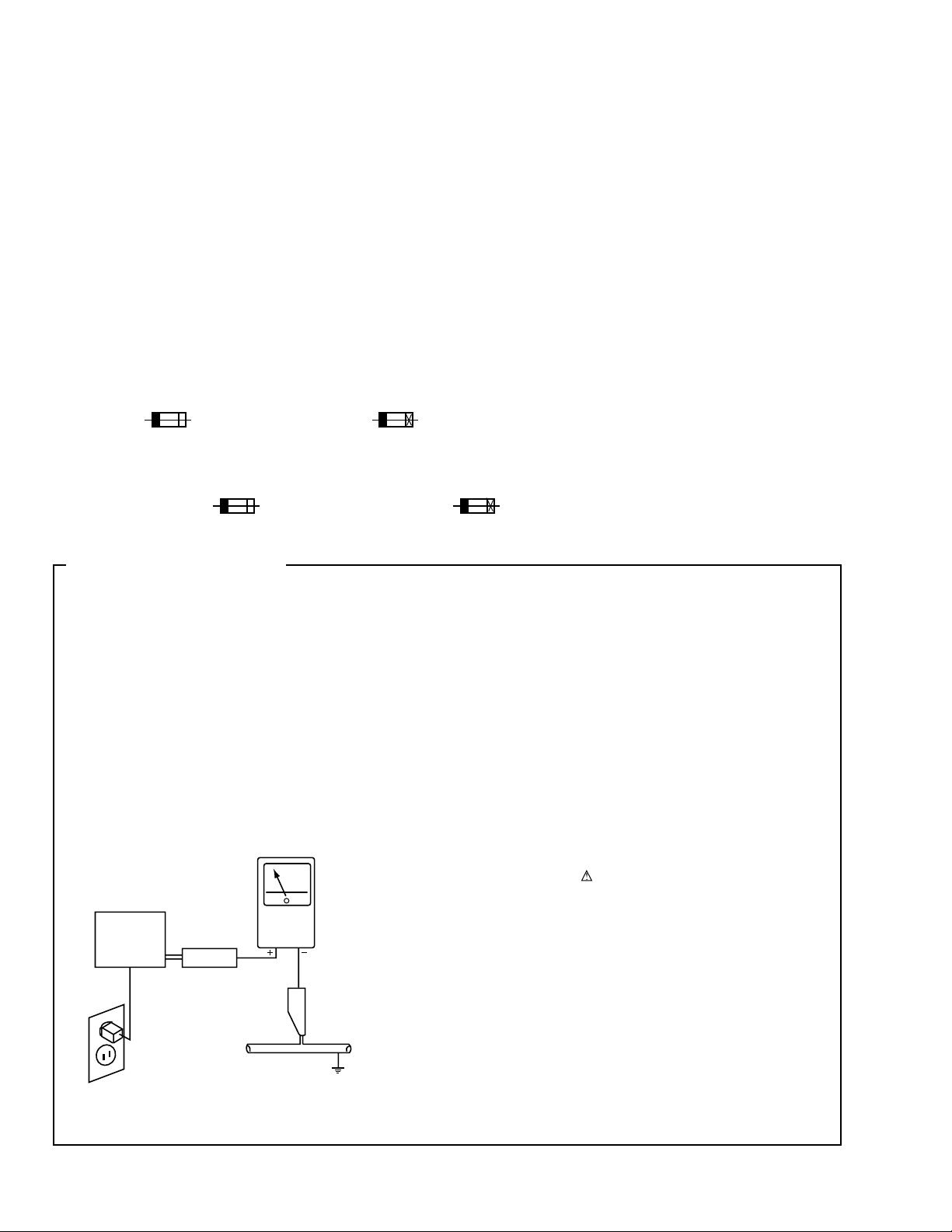
LEAKAGE CURRENT CHECK
Measure leakage current to a known earth ground (water
pipe, conduit, etc.) by connecting a leakage current tester
such as Simpson Model 229-2 or equivalent between the
earth ground and all exposed metal parts of the appliance
(input/output terminals, screwheads, metal overlays, control
shaft, etc.). Plug the AC line cord of the appliance directly
into a 120V AC 60Hz outlet and turn the AC power switch
on. Any current measured must not exceed 0.5mA.
Reading should
not be above
0.5mA
Earth
ground
Device
under
test
Also test with
plug reversed
(Using AC adapter
plug as required)
Leakage
current
tester
Test all
exposed metal
surfaces
ANY MEASUREMENTS NOT WITHIN THE LIMITS
OUTLINED ABOVE ARE INDICATIVE OF A POTENTIAL
SHOCK HAZARD AND MUST BE CORRECTED BEFORE
RETURNING THE APPLIANCE TO THE CUSTOMER.
2. PRODUCT SAFETY NOTICE
Many electrical and mechanical parts in the appliance
have special safety related characteristics. These are
often not evident from visual inspection nor the protection
afforded by them necessarily can be obtained by using
replacement components rated for voltage, wattage, etc.
Replacement parts which have these special safety
characteristics are identified in this Service Manual.
Electrical components having such features are identified
by marking with a
in this Service Manual.
The use of a substitute replacement component which does
not have the same safety characteristics as the PIONEER
recommended replacement one, shown in the parts list in
this Service Manual, may create shock, fire, or other hazards.
Product Safety is continuously under review and new
instructions are issued from time to time. For the latest
information, always consult the current PIONEER Service
Manual. A subscription to, or additional copies of, PIONEER
Service Manual may be obtained at a nominal charge from
PIONEER.
on the schematics and on the parts list
AC Leakage Test
2
Page 3
XV-HTD510, XV-HTD510-B
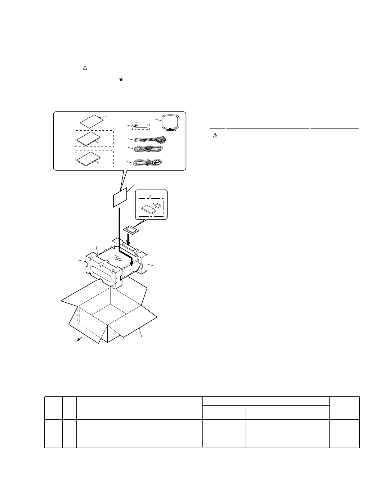
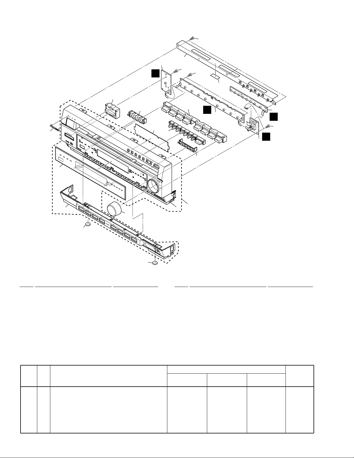
2. EXPLODED VIEWS AND PARTS LIST
NOTES:• Parts marked by "NSP" are generally unavailable because they are not in our Master Spare Parts List.
2.1 PACKING
The mark found on some component parts indicates the importance of the safety factor of the part.
•
Therefore, when replacing, be sure to use parts of identical designation.
Screws adjacent to mark on the product are used for disassembly.
•
KUXJ
Type
Only
KCXJ,
KUCXJ
Types
Only
12
6
13
14
10
7
2
3
1
15
11
4
5
8
(1) PACKING PARTS LIST
Mark No. Description Part No.
1 Power Cord ADG7022
2 FM Antenna ADH7004
3 Video Cord (L = 1.5m) VDE1053
4 Remote Control Unit See Contrast table (2)
5 Battery Cover XZN3117
NSP 6 Dry Cell Battery (R6P, AA) VEM-013
7 Pad F XHA3124
8 Pad R XHA3125
9 Packing Case See Contrast table (2)
10 Packing Sheet AHG7010
NSP 11 Polyethylene Bag Z21-038
NSP 12 Warranty Card ARY7045
13 Operating Instructions (English) See Contrast table (2)
14 Operating Instructions See Contrast table (2)
(English/French)
15 AM Loop Antenna ATB7009
9
FRONT
(2) CONTRAST TABLE
XV-HTD510/KUXJ, KCXJ and XV-HTD510-B/KUCXJ are constructed the same except for the following :
Part No.
Mark No. Symbol and Description
4
Remote Control Unit
9
Packing Case
13
Operating Instructions (English)
14
Operating Instructions
(English/French)
XV-HTD510
/KUXJ
XXD3033
XHD3171
XRB3009
Not used
XV-HTD510
/KCXJ
XXD3033
XHD3171
Not used
XRE3039
XV-HTD510-B
/KUCXJ
XXD3032
XHD3192
Not used
XRE3039
Remarks
DSP Button
3
Page 4
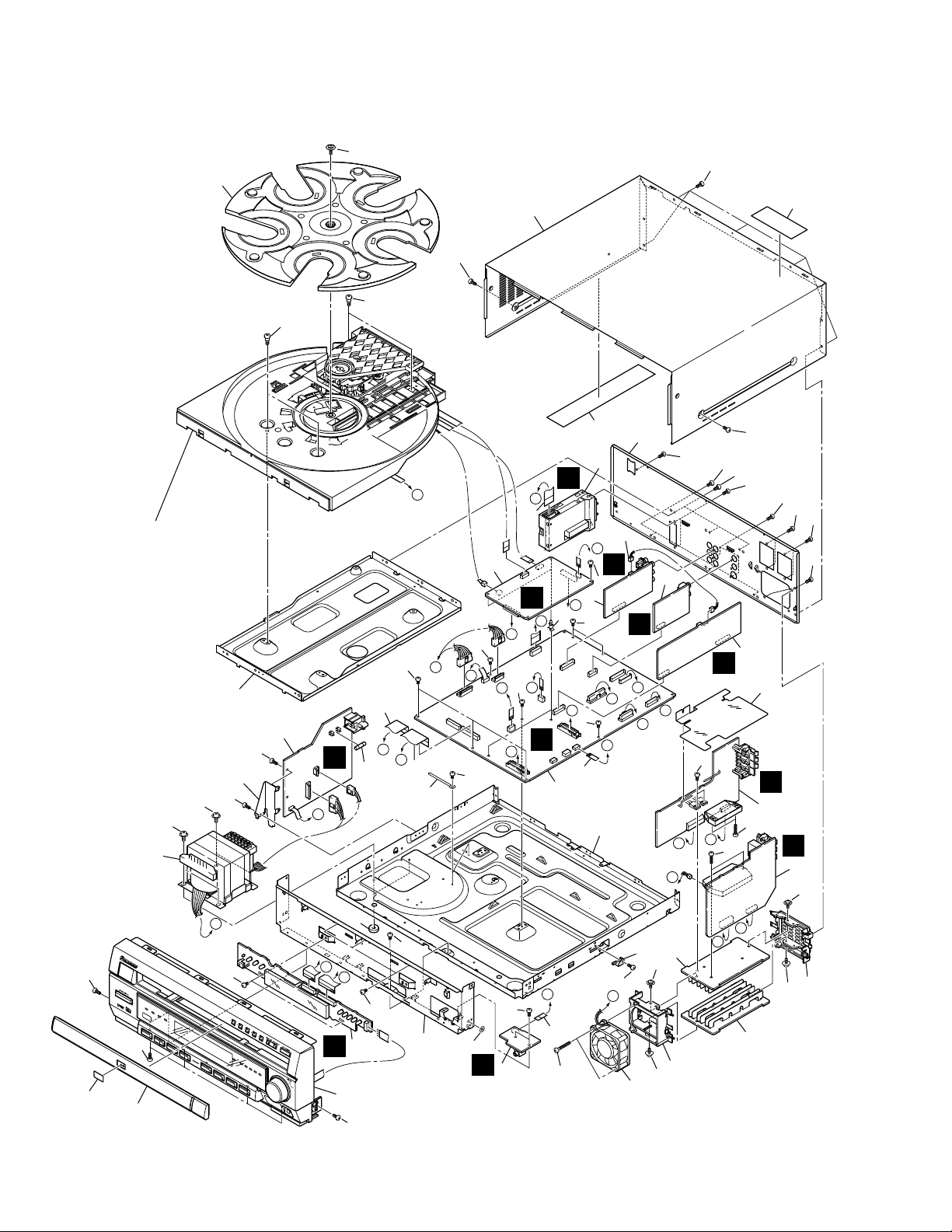
XV-HTD510, XV-HTD510-B
2.2 EXTERIOR
31
Refer to
"2.4 TABLE MECHANISM SECTION".
26
43
25
43
42
42
12
41
23
44
47
47
38
22
11
J
M
43
43
C
D
16
2
A
T
D
B
13 17
39
43
O
15
20
K
1
F
33
O
L
43
E
M
I
L
9
K
43
7
N
43
L
J
I
N
43
19
G
K
21
44
37
44
48
43
43
48
48
48
48
48
8
10
M
32
H
44
H
4
45
J
I
45
F
G
3
40
29
43
A
B
43
24
5
N
Refer to
"2.3 FRONT PANEL SECTION".
44
49
O
H
30
G
34
40
28
28
27
40
E
43
18
6
46
43
F
40
14
44
35
C
43
44
36
4
Page 5

(1) EXTERIOR PARTS LIST
XV-HTD510, XV-HTD510-B
Mark No. Description Part No.
1 DVDM Assy XWX3034
2 PRIMARY Assy XWZ3432
3 FRONT AMP Assy XWZ3438
4 REAR AMP Assy XWZ3442
5 DISPLAY Assy XWZ3446
6 MIC HP Assy XWZ3450
7 INPUT Assy XWZ3455
8 VIDEO Assy XWZ3459
9 MAIN Assy XWX3030
10 DSP Assy XWX3040
11 TUNER MODULE AXQ7228
12 T1 Power Transformer XTS3051
13 FU1 Fuse (5A) REK1067
14 DC Fan Motor AXM7014
15 13P F.F.C/60V XDD3089
(MAIN CN5701 – TUNER CN201)
16 19P F.F.C/60V XDD3090
(MAIN CN5509 – DISPLAY CN5801)
17 27P F.F.C/60V XDD3091
(MAIN CN5511 – DISPLAY CN5802)
18 5P F.F.C/60V XDD3093
(MAIN CN5501 – MIC HP CN5807)
19 7P F.F.C/60V XDD3094
(MAIN CN8902 – DVDM CN55)
20 Connector Assy 3P XDE3041
(INPUT CN5207 – DSP CN3703)
NSP 21 Chassis XNA3008
Mark No. Description Part No.
27 DV Bracket XNG3064
28 Heat Sink XNH3021
NSP 29 Spacer XEB3019
30 Fan Mold AMR7321
31 Rotary Tray VNK4739
32 Barrier H XEC3016
NSP 33 PCB Support XEC3020
34 Rear Mold XMR3038
35 DVDV Badge XAM3003
36 Tray Cap See Contrast table (2)
37 65 Label ARW7050
NSP 38 Large Label XAX3217
39 Cord Clamper RNH-184
40 Screw ABA1021
41 Screw ABA7069
42 Screw ASZ40P060FMC
43 Screw BBZ30P060FMC
44 Screw BBZ30P080FZK
45 Screw BBZ30P160FMC
46 Screw BPZ30P350FZK
47 Screw PBA1106
48 Screw VPZ30P080FZK
49 Washer VEC1254
22 Rear Panel See Contrast table (2)
23 Bonnet Case See Contrast table (2)
24 Front Frame XNG3056
25 PCB Angle XNG3057
26 Mecha Frame XNG3059
(2) CONTRAST TABLE
XV-HTD510/KUXJ, KCXJ and XV-HTD510-B/KUCXJ are constructed the same except for the following :
Part No.
Mark No. Symbol and Description
22
Rear Panel
23
Bonnet Case
36
Tray Cap
XV-HTD510
/KUXJ
XNC3094
XZN3118
XAN3032
XV-HTD510
/KCXJ
XNC3094
XZN3118
XAN3032
XV-HTD510-B
XNC3097
XZN3119
XAN3033
Remarks
/KUCXJ
5
Page 6
XV-HTD510, XV-HTD510-B
2.3 FRONT PANEL SECTION
12
13
7
6
9
14(1/2)
Q
15
19
10
16
19
19
18
11
8
5
P
14(2/2)
2
3
S
19
R
1
4
17
17
(1) FRONT PANEL SECTION PARTS LIST
Mark No. Description Part No.
NSP 1 JOG Assy XWZ3448
2 KEYB Assy XWZ3447
NSP 3 DISC KEY Assy XWZ3449
NSP 4 STBY SWITCH Assy XWZ3453
NSP 5 Front Panel Assy See Contrast table (2)
6 Front Cap See Contrast table (2)
7 Display Panel See Contrast table (2)
8 Front Panel See Contrast table (2)
9 Volume Knob See Contrast table (2)
10 Disc Button See Contrast table (2)
Mark No. Description Part No.
11 Function Button See Contrast table (2)
12 Power Button See Contrast table (2)
13 Pioneer Badge XAM3001
14 Lens XAX3216
15 FL Filter XEC3015
16 Top Frame XNG3063
17 Leg AEB7090
NSP 18 Small Label XAX3291
19 Screw VPZ30P080FZK
(2) CONTRAST TABLE
XV-HTD510/KUXJ, KCXJ and XV-HTD510-B/KUCXJ are constructed the same except for the following :
Part No.
Mark No. Symbol and Description
NSP
5
Front Panel Assy
6
Front Cap
7
Display Panel
8
Front Panel
9
Volume Knob
10
Disc Button
11
Function Button
12
power Button
XV-HTD510
/KUXJ
XXG3070
XAK3212
XAK3213
XMB3047
XAA3020
XAD3093
XAD3100
XAD3101
XV-HTD510
/KCXJ
XXG3070
XAK3212
XAK3213
XMB3047
XAA3020
XAD3093
XAD3100
XAD3101
XV-HTD510-B
Remarks
/KUCXJ
XXG3071
XAK3227
XAK3229
XMB3048
XAA3021
XAD3099
XAD3094
XAD3095
6
Page 7
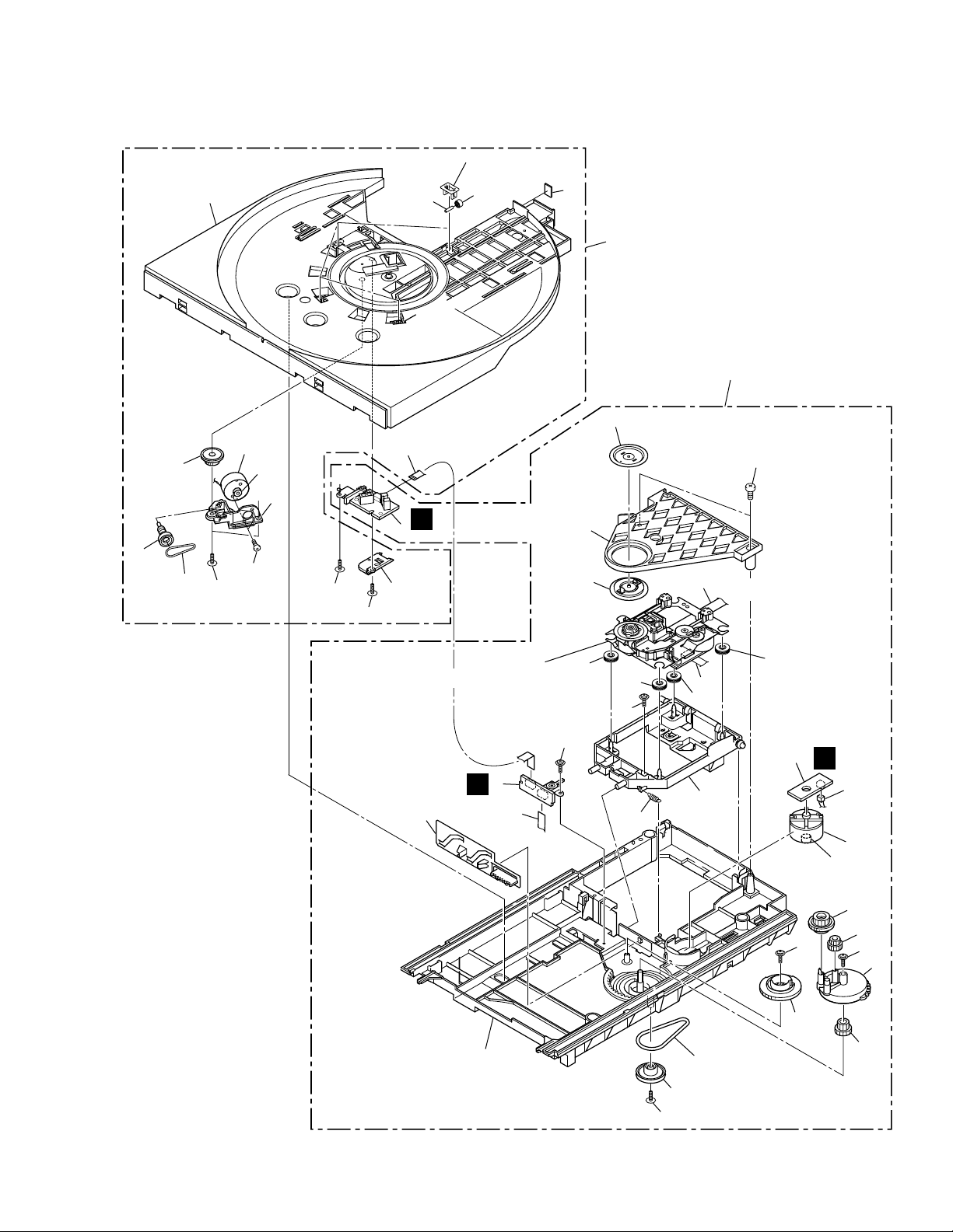
2.4 TABLE MECHANISM SECTION
37
(1/6)
37
(2/6 - 5/6)
[Roller Cover]
37
(6/6)
[PCB Cover]
36
35
2
1
16
29
20
18
14
30
28
21
14
14
19
32
13
14
11
12
26
25
30
30
27
22
15
17
38
33
40
34
42
39
31
10
5
7
8
3
4
42
9
6
From
DVDM CN555
From
DVDM CN2
Refer to
"2.5 TRAVERSE MECHANISM ASSY-S".
43
42
41
24
23
30
B
A
C
XV-HTD510, XV-HTD510-B
7
Page 8

XV-HTD510, XV-HTD510-B
TABLE MECHANISM SECTION PARTS LIST
Mark No. Description Part No.
NSP 1 5C Mech. Base Assy XXA3027
NSP 2 5C Table Mech. Assy VWT1175
NSP 3 TRSB Assy XWZ3461
NSP 4 SSRB Assy XWZ3462
NSP 5 LOMB Assy XWZ3463
6 Traverse Mechanism Assy-S VXX2653
7 Flexible Cable 24P XDD3074
8 Flexible Cable 8P (T) XDD3075
9 Flexible Cable 8P (M) XDD3076
10 Housing Assy 2P XDE3039
11 Slider Motor (LOADING) VXM1033
12 Motor Pulley PNW1634
13 Spring VBH1333
14 Floating Rubber VEB1286
15 Load Belt VEB1316
16 Clamper Plate VNE2162
17 Mechanism Base VNK4826
18 Clamper VNL1738
19 Float Base VNL1907
20 Clamper Holder VNL1872
21 Clamp Cam VNL1873
22 Planet Base VNL1874
23 Gear Pulley VNL1876
24 Loading Gear (1) VNL1877
25 Loading Gear (2) VNL1908
26 Drive Gear VNL1879
27 Change Gear VNL1904
28 Screw ABA7009
29 Screw BPZ30P080FMC
30 Screw Z39-019
31 Motor (TRAY) DXM1118
32 Flexible Cable (7P) VDA1835
33 Motor Pulley PNW1634
34 Tray Belt VEB1317
35 Rubber Roller VEB1318
36 Roller Shaft VLL1511
37 Slide Table VNK4751
38 Motor Holder VNL1880
39 Worm Gear VNL1881
40 Tray Gear VNL1882
41 Screw JGZ17P028FMC
42 Screw Z39-019
43 CR Cushion 2 XEB3020
8
Page 9
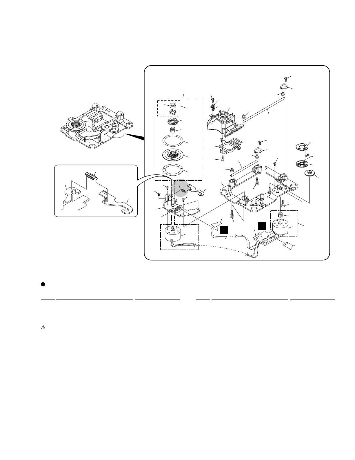
2.5 TRAVERSE MECHANISM ASSY-S
XV-HTD510, XV-HTD510-B
• Top View
17
37
32
29
18
26
11
25
27
7
3
36
35
30
16
9
31
37
21
17
24
34
19
8
6
20
12
9
37
4
21
22
33
33
23
28
10
15
2
E
10
5
10
13
37
10
14
7
18
7
1
D
To
DVDM Assy
CN3
TRAVERSE MECHANISM ASSY-S PARTS LIST
Mark No. Description Part No. Mark No. Description Part No.
NSP 1 SMEB Assy VWG2048
NSP 2 FGSB Assy VWG2009
NSP 3 Motor (CARRIAGE) VXM1079
NSP 4 Motor (SPINDLE) VXM1084
NSP 5 Pickup Assy VWY1055
6 Table Sheet DEC2040
7 Screw VBA1058
8 Centering Spring VBH1278
9 Hook Spring VBH1317
10 Skew Spring VBH1303
11 Gear Spring VBH1308
NSP 12 Reflected Sheet VEC1959
13 Guide Bar VLL1504
14 Sub-guide Bar VLL1505
15 Hold Spring VNC1017
NSP 16 Magnet Holder VNE2070
NSP 17 Motor Base VNE2154
NSP 18 Cover VNE2155
19 Centering Ring VNL1746
NSP 20 Disc Table VNL1747
NSP 30 Magnet VYM1024
21 Hook VNL1770
22 FFC Holder VNL1802
23 Mechanism Base VNL1806
24 FG Holder VNL1807
25 Gear A VNL1808
26 Gear B VNL1809
27 Gear C VNL1810
28 Slider VNL1811
29 Gear D VNL1814
31 Screw JFZ17P025FZK
32 Screw JGZ17P028FMC
33 Screw VBA1051
34 Magnet Holder Assy VXX2507
35 Spindle Motor Assy VXX2649
36 Carriage Motor Assy VXX2650
37 Screw PBA1069
9
Page 10
1
23
XV-HTD510, XV-HTD510-B
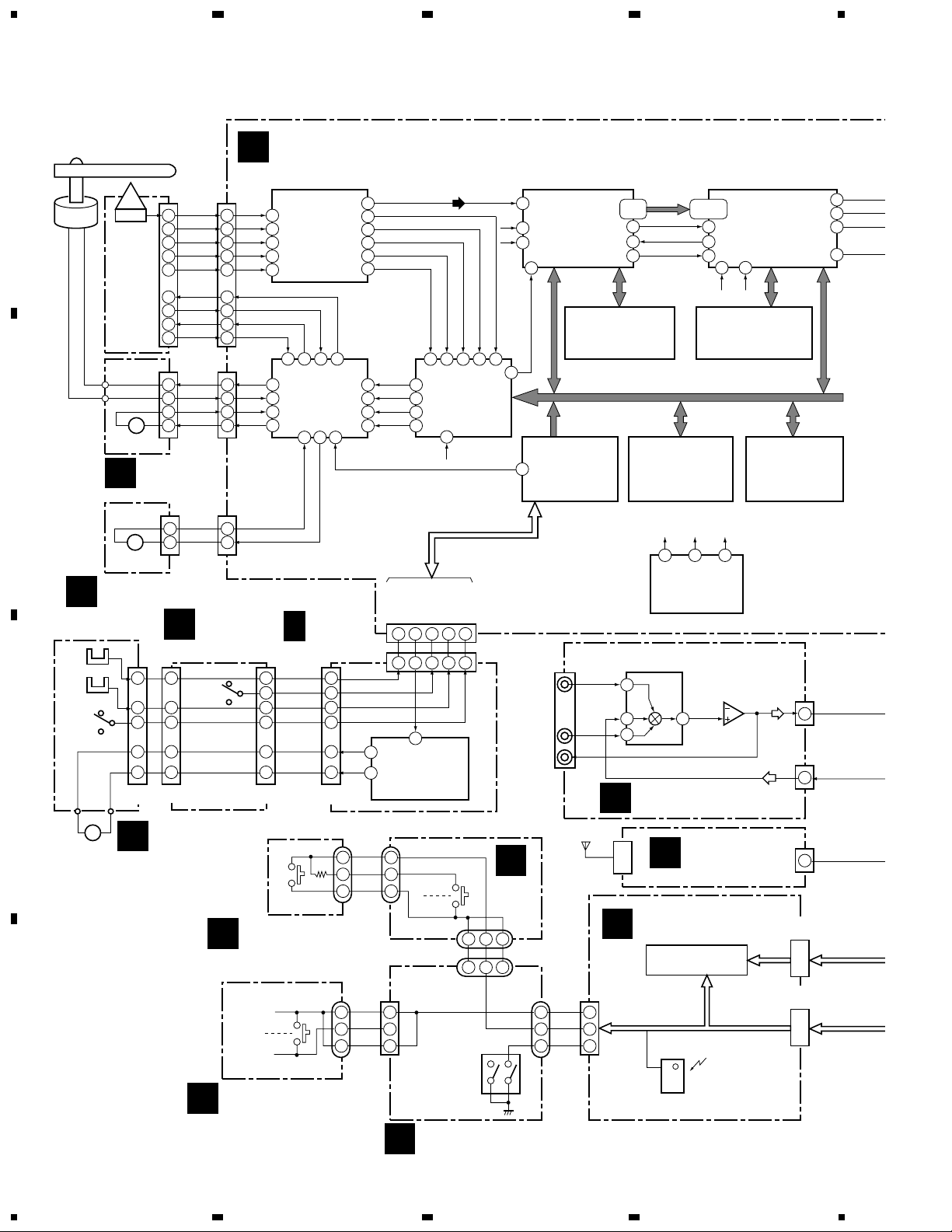
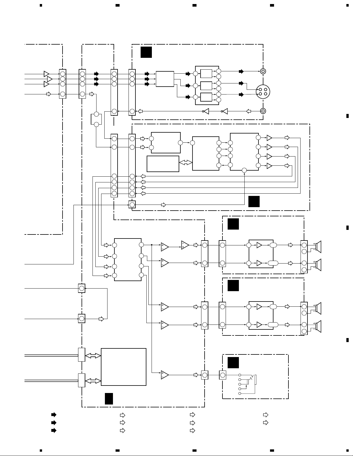
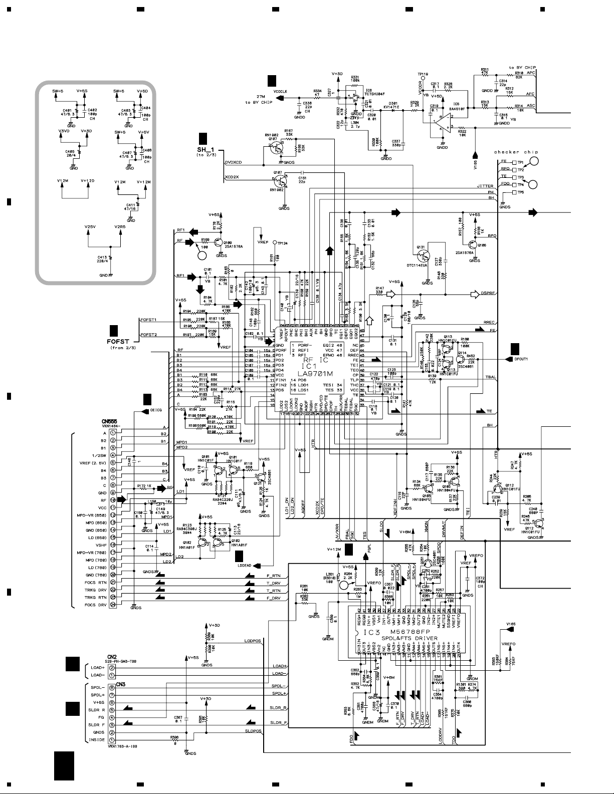
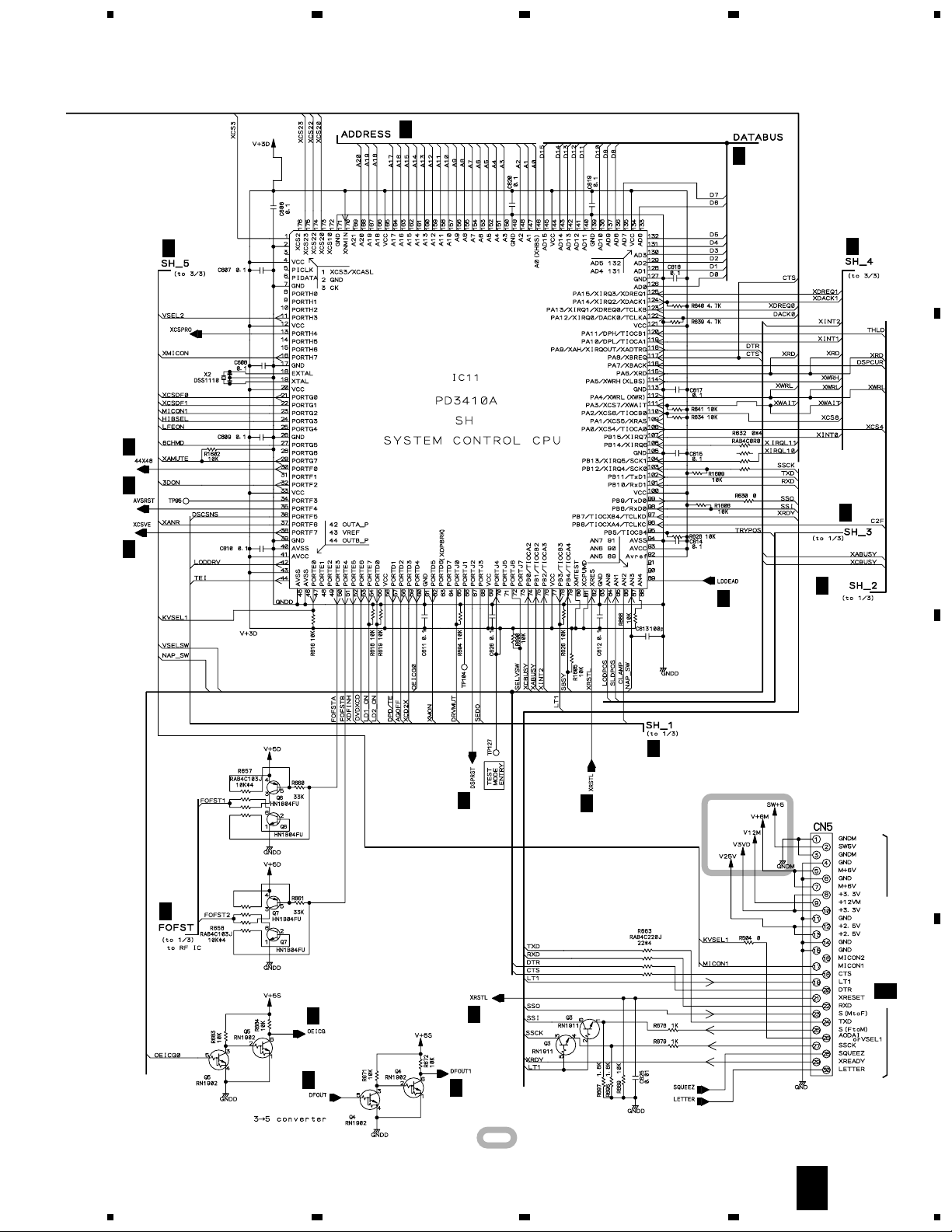
3. BLOCK DIAGRAM AND SCHEMATIC DIAGRAM
3.1 BLOCK DIAGRAM
DVDM ASSY
S11
CN555
10
3
2
7
6
24
23
22
21
CN3
(8P)
7
8
5
3
CN2
1
2
F
(24P)
RF
B1
B2
B3
B4
LOADLOAD+
CN11
(8P)
3
6
7
8
9
31
32
34
35
4
3
5
6
7
8
DISC SENS
TRAY POS
LOAD POS
54
IC1
LA9701M
RF IC
9 12 13 10
IC3
M56788FP
SPDL & FTS
DRIVER
15 14 17
46
56
57
42
35
3
20
37
28
LODDRV LODDRV
I 1/2
MAIN ASSY
5
CLAMP
6
4
3
SEDR+
2
12
SEDR-
1
13
CN8903
(8P)
3
2
1
RFO
DSP RF
BH
PH
FE
TE
32 33 30 31 39
FDO
47
48
45
SERVO DSP
46
16M
DISC SENS
SEDO
34 125
54 763
25
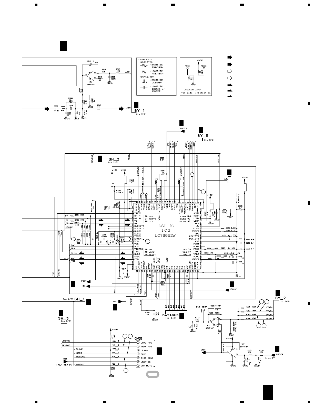
LC78652W
14
CLAMP
TDO
SLDO
SPDO
IC8901
BA6195FP
5DISC
TURN DRIVER
KEYB ASSY
J5811J5811
3
2
1
IC2
TRAY POS
LOAD POS
CN55
CN8902
(7P)
(7P)
170
27M
4
DVD DECODER
16M
107
12
3
PD3410A
42
SYSTEM
CONTROL CPU
JA5201
TV/VCR
IN
AUX IN
AUX OUT
P
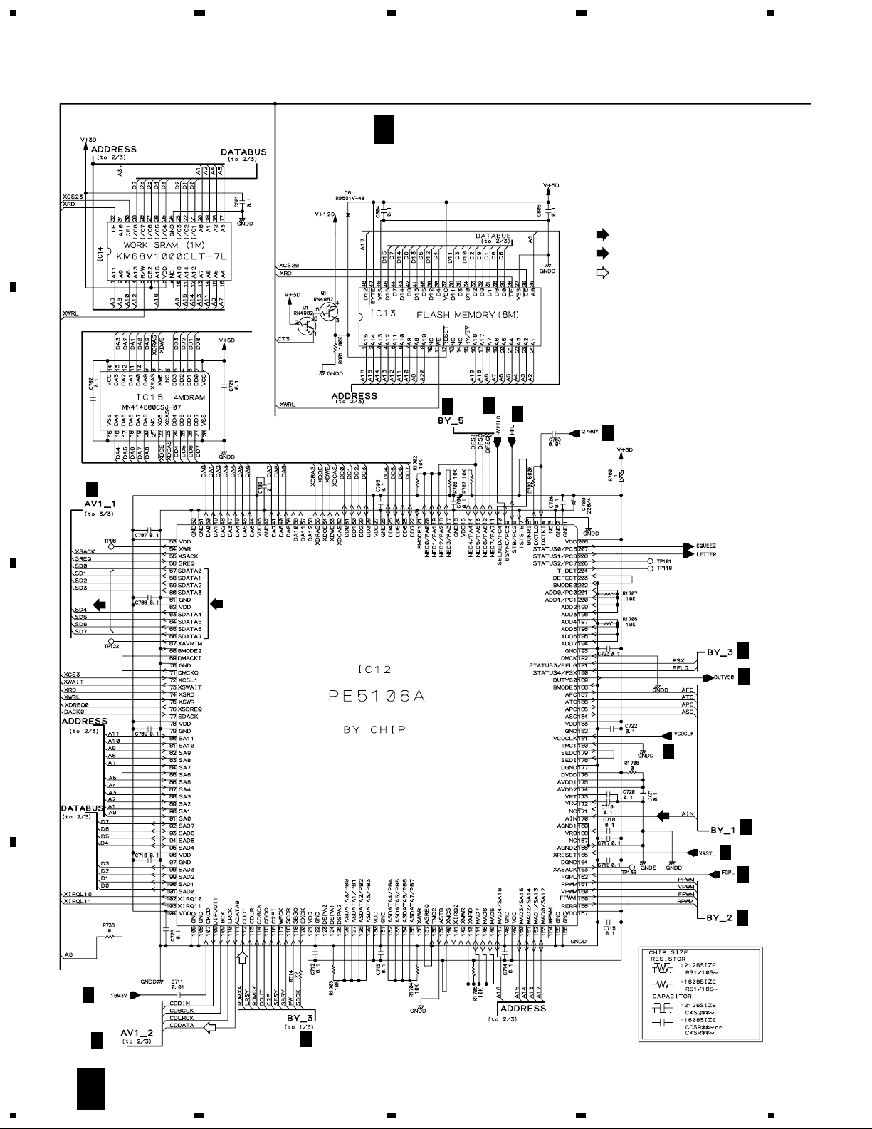
IC12
PE5108A
BY CHIP
IC15
MN414800CSJ-07
4M DRAM
IC11
IC5231
AUDIO SELECTOR
K
ANT
A
(24P)
Spindle
Motor
OEIC
PICKUP
ASSY
CN202
(8P)
+-
M
Carriage
Motor
B
D
SMEB
RF
15
B1
22
B2
23
B3
18
B4
19
F DRV
1
T RTN
2
T DRV
3
F RTN
4
SPDL+
7
SPDL-
8
SLDR R
5
SLDR F
3
ASSY
CN31
2
+-
1
M
Loading
Motor
LOMB ASSY
C
A
PC21
PC22
S21
LOADING
POSITION
DET. SW
C
+-
M
TRAY
Motor
SSRB ASSY
TRSB ASSY
3
5
1
7
5
3
2
6
4
4
CN12
CN21
(7P)
(7P)
B
DISC
CLAMP
DET. SW
SD0-SD7
57-60
63-66
111
56
55
CDDATA
SREQ
XSACK
80-84
78,86,87
54
91
89
MB811171622A-100FN
IC14
KM68V1000CLT-7L
WORK SRAM
(1M)
27M1316M936/16M
3
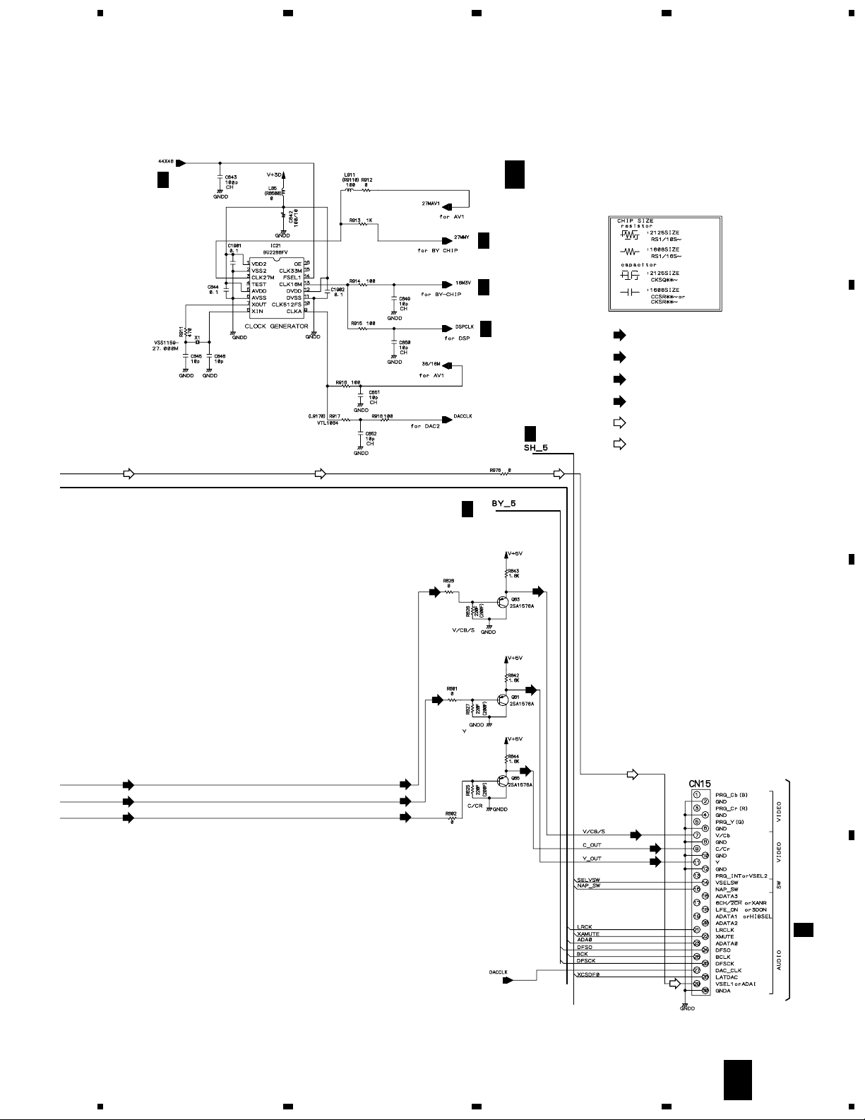
IC21
BU2288FV
CLOCK
GENERATOR
BU4052BCF
11
1314
15
INPUT ASSY
TUNER
J
MODULE
4
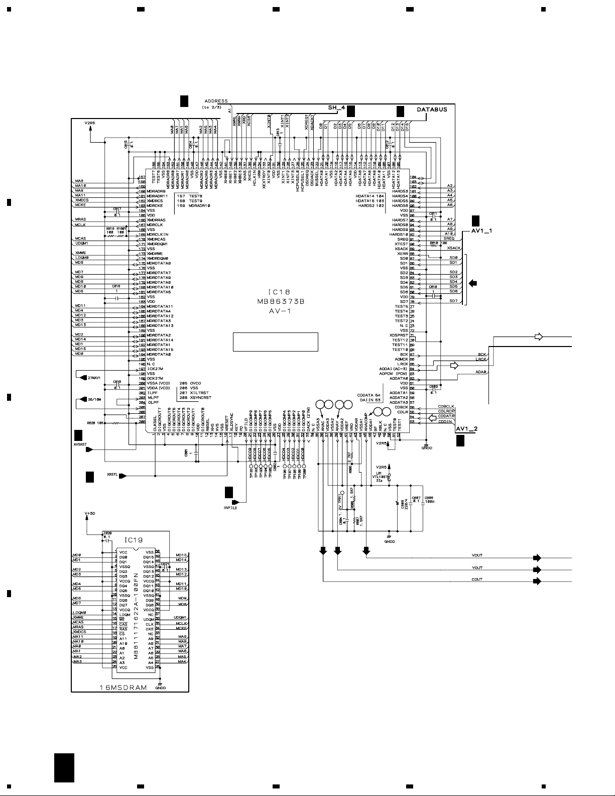
IC18
MB86373B
MPEG2
DECODER
AV-1
197
205
27M
36/16M
IC19
16M SDRAM
MEMORY (8M)
IC5352-1/2
CN5207
2
1
3
CN5208
IC13
VYW3003
FLASH
(3P)
(FL)
3
(19P)
(TX)
6
CN201
(13P)
7
45
39
36
64
L
TXL
L CH
STBY SWITCH
Q
ASSY
J5805
3
2
1
D
DISC KEY ASSY
S
J5808
J5808
CN5806
3
2
1
VOLUME
JOG ASSY
R
S5801
JOG
1
3
2
1
3
2
J5804
(5P)
4
3
2
4
3
2
DISPLAY ASSY
N
V5801 XAV3011
CN5803
(5P)
FL TUBE
REMOTE
SENSOR
CN5801
(19P)
CN5802
(27P)
10
1234
Page 11
(DVD)
CN15
(30P)
Q83
Q81
Q85
5
678
XV-HTD510, XV-HTD510-B
VIDEO ASSY
L
CN8501
CN5352
(30P)
11
29
7
9
(VCB)
(DVD)
IC8351
V/Cb
7
Y
11
C/Cr
9
AODAI
AC-3
29
(11P)
(Y)
(C)
13
12
TC74HCT7007AF
11
CN3001
(21P)
15
21
17
11
4
8
6
3
1
VIDEO
Y
C/Cr
DIN
DIN
AODAI
SW
C
SL
FL
CN5351
(11P)
4
8
6
11
CN3702
(21P)
(DI)
3
(DVD)
1
15
21
17
11
CN3703
(3P)
3
(VCB)
(Y)
(C)
3
4
W24257AJ-12
256k SRAM
(SW)
(C)
(SL)
(FL)
VIDEO
FILTER
IC8801
LC89056W-E
DIR
IC3851
(FL)
IC5351 LA7138M
VIDEO AMP
(VCB)
3
(Y)
10
(C)
6
IC5104-2/3 IC5104-1/3
16
85
IC3801
YSS912C-F
AMP
AMP
AMP
DSP
21
23
13
15
17
19
45
84
(VCB)
(Y)
(C)
IC3751
647
AK4527BVQ
746
6 ch
8
CODEC
9
30
JA5351
VIDEO OUT
Y
C
(DI)(DI)
M
JA5103
DIGITAL IN
IC8701-2/2
67
27
IC8703-1/2
21
25
IC8705-1/2
21
24
IC8705-2/2
6
23
DSP ASSY
CN5352
S-VIDEO OUT
(FL)
(SL)
(C)
(SW)
7
A
B
CN5209
(19P)
6
CN5701
(13P)
7
CN5509
(19P)
CN5511
(27P)
(FL)
17
(SL)
(C)
(SW)
(TX)
IC3001
9
M62446FP
E-VOL
11
6
IC5501
PDC076A
MICROCOMPUTER
IC3151,IC3152,IC3161,IC3171:
BA4558F
IC3151-1/2
31
36
34
33
5
6
IC3171-2/2
5
6
IC3161-1/2
5
6
IC3161-2/2
3
2
IC3902-1/2
5
6
7
7
7
1
7
IC3151-1/2
6
5
(FL)
7
(SW)
CN3051
(15P)
CN3052
(13P)
(SL)
(C)
(HP)
CN5501
(5P)
FRONT AMP ASSY
G
IC3301
CN3301
(15P)
FL IN
2
6
6
10
5
SW IN
SL IN
C IN
LOUT
2
6
CN3501
(13P)
6
10
1
CN5807
(5P)
REAR AMP ASSY
H
MIC HP ASSY
O
STK413-000
POWER AMP
13
18
IC3401
STK402-230
POWER AMP
1
15
PHONES
8,9
20,21
6,7
18,19
CN3303
(FL)
(SW)
CN3401
(SL)
(C)
(6P)
(6P)
6
5
2
1
FL
SP
SW
SP
C
1
2
5
6
SL
SP
C
SP
(VCB)
: VCB SIGNAL ROUTE
(Y)
: Y SIGNAL ROUTE
(C)
: C SIGNAL ROUTE
I 2/2
(DVD)
MAIN ASSY
: DVD AUDIO SIGNAL ROUTE
(DI)
: DI AUDIO SIGNAL ROUTE
(FL)
: FL AUDIO SIGNAL ROUTE
(HP)
: HP AUDIO SIGNAL ROUTE
(SL)
: SL AUDIO SIGNAL ROUTE
(C)
: C AUDIO SIGNAL ROUTE
(SW)
: SW AUDIO SIGNAL ROUTE
(TX)
: TX AUDIO SIGNAL ROUTE
11
D
5
6
7
8
Page 12
1
XV-HTD510, XV-HTD510-B
3.2 OVERALL WIRING DIAGRAM
A
23
TUNER MODULE
J
(AXQ7228)
FM
AM
INPUT ASSY
K
(XWZ3455)
4
AC 120V
50/60Hz
POWER CORD
ADG7022
LIVE
NEUTRAL
PICKUP ASSY
(VWY1055)
T
B
C
PRIMARY ASSY
(XWZ3432)
(F)
(T)
(T)
(F)
E
TRAVERSE MECHANISM ASSY-S (VXX2653)
FGSB ASSY
(VWG2009)
5CH MECH.BASE ASSY
(XXA3027)
B
SSRB ASSY
(XWZ3462)
D
SMEB ASSY
(VWG2048)
LOMB ASSY
C
(XWZ3463)
A
TRSB ASSY
(XWZ3461)
(F)
(T)
(T)
(F)
: RF SIGNAL ROUTE
(F)
: FOCUS SERVO LOOP LINE
(T)
: TRACKING SERVO LOOP LINE
(S)
D
: SLIDER SERVO LOOP LINE
Q
STBY SWITCH
ASSY
(XWZ3453)
DISPLAY ASSY
N
(XWZ3446)
KEYB ASSY
P
(XWZ3447)
12
1234
Page 13
5
678
XV-HTD510, XV-HTD510-B
Note : When ordering service parts, be sure to refer to "EXPLODED VIEWS and PARTS LIST" or "PCB PARTS LIST".
M
DSP ASSY (XWX3040)
F
M 1/2- M 2/2
F 1/3- F 3/3
DVDM ASSY
(XWX3034)
VIDEO ASSY
L
(XWZ3459)
I 1/3- I 3/3
I
MAIN ASSY (XWX3030)
DC FAN MOTOR
AXM7014
G
FRONT AMP
ASSY
(XWZ3438)
A
B
H
C
D
R
JOG ASSY
(XWZ3448)
MIC HP ASSY
O
(XWZ3450)
REAR AMP
ASSY
(XWZ3442)
S
DISC KEY ASSY
(XWZ3449)
13
5
6
7
8
Page 14
1
23
XV-HTD510, XV-HTD510-B
3.3 TRSB, SSRB, LOMB, SMEB and FGSB ASSYS
4
A
: The power supply is shown with the marked box.
TRSB ASSY (XWZ3461)
A
CN8903
SSRB ASSY (XWZ3462)
B
I 3/3
B
C
LOMB ASSY (XWZ3463)
C
CARRIAGE MOTOR (LOADING)
D
: VXM1033
F 1/3
CN2
14
A
B C
1234
Page 15
5
678
XV-HTD510, XV-HTD510-B
A
(S)
: SLIDER SERVO LOOP LINE
FGSB ASSY
E
(VWG2009)
SMEB ASSY (VWG2048)
D
B
F 1/3
CN3
(S)
(S)
CARRRIAGE MOTOR
ASSY : VXX2650
SPINDLE MOTOR ASSY
: VXX2649
C
D
D
5
6
7
E
8
15
Page 16
1
XV-HTD510, XV-HTD510-B
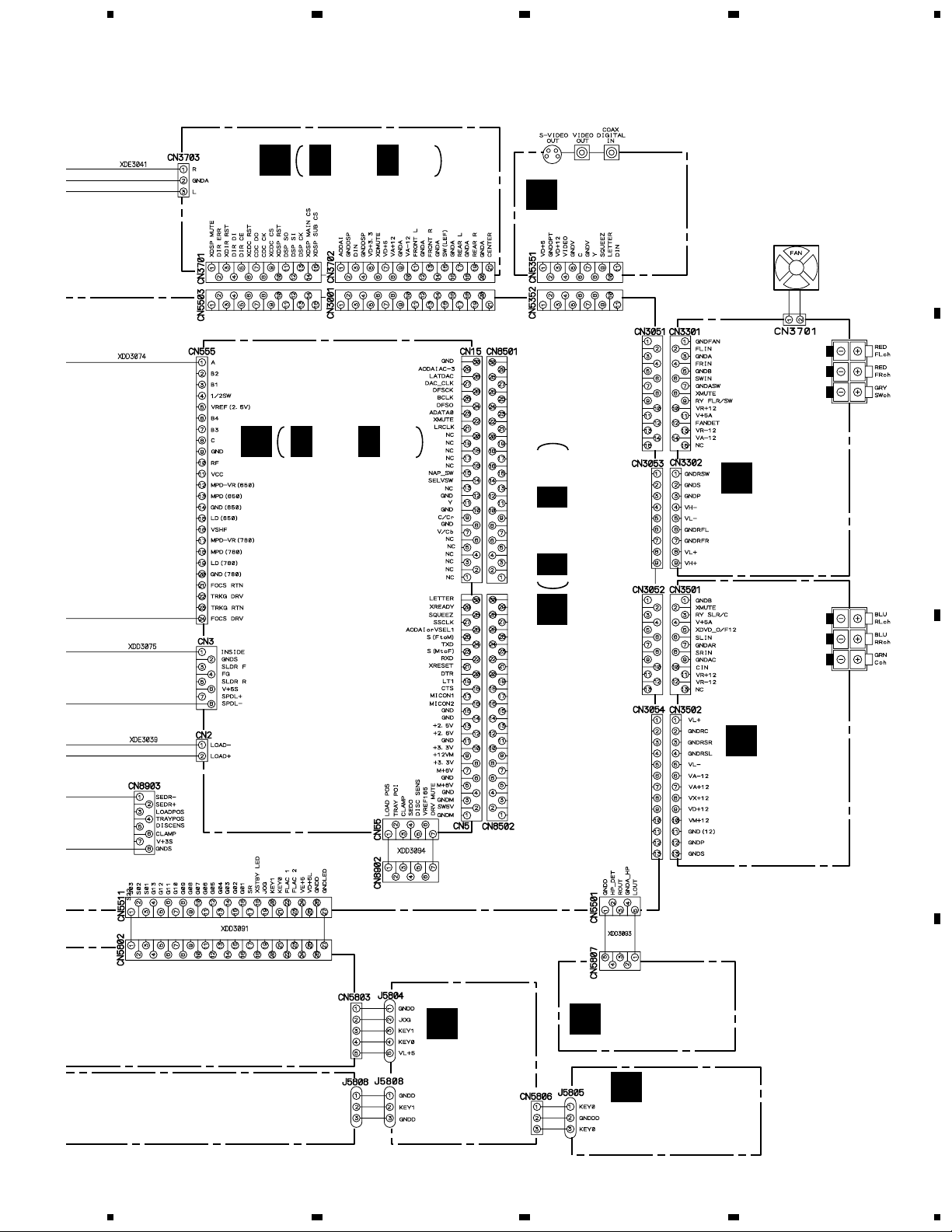
3.4 DVDM ASSY (1/3)
A
23
F
2/3
1/2
F
2/3
4
2
4
(V)
1
B
F
2/3
F
2/3
C
(V)
(A)
(A)
(A)
(F)
(F)
(T)(T)
(V)
F
2/3
(S)
PICKUP ASSY
F
2/3
(F)
(T)
(T)
(F)
(F)
(T)
(T)
(F)
F
2/3
7
(S)
(S)
C
CN31
D
(S)
(S)
(F)
16
D
CN202
1/3
F
1234
(S)
(S)
(T)
(T)
(F)
(F)
(T)
Page 17
5
678
XV-HTD510, XV-HTD510-B
F 1/3
(V) (V)
DVDM ASSY (XWX3034)
2/2
F
2/3
: RF SIGNAL ROUTE
(V)
: RF VIDEO SIGNAL ROUTE
(A)
: RF AUDIO SIGNAL ROUTE
(AD)
: AUDIO DATA SIGNAL ROUTE
(F)
: FOCUS SERVO LOOP LINE
(T)
: TRACKING SERVO LOOP LINE
(S)
: SLIDER SERVO LOOP LINE
F
2/3
F
3/3
F
2/3
F
2/3
(AD)
6
A
B
(T)
(F)
(A)
(S)
(F)
(T)
F
2/3
F
2/3
F
2/3
(T)
(F)
(A)
5
(S)
(F)
(T)
F
2/3
F
2/3
8
9
F
2/3
F
19 20
2/3
VNK1493
I 3/3
2/2
1/2
10 11
F
2/3
C
D
CN8902
18
5
6
: The power supply is shown with the marked box.
F
7
1/3
8
17
Page 18
1
XV-HTD510, XV-HTD510-B
3.5 DVDM ASSY (2/3)
23
4
A
F 2/3
VYW3003
B
F
3/3
DVDM ASSY (XWX3034)
(V)
: RF VIDEO SIGNAL ROUTE
(VD)
: VIDEO DATA SIGNAL ROUTE
(AD)
: AUDIO DATA SIGNAL ROUTE
F
3/3
3/3
F
1/3
F
F
3/3
(VD)
C
D
F
3/3
(VD)
(AD)
F
1/3
F
1/3
F
1/3
(V)
F
1/3
F
3/3
F
1/3
F
1/3
18
F
3/3
2/3
F
1234
(AD)
F
1/3
Page 19
5
678
XV-HTD510, XV-HTD510-B
F
1/3, 3/3
F
1/3, 3/3
F
F
3/3
20MHz
F
3/3
F
3/3
3/3
A
B
F
1/3
F
3/3
F
F
1/3
F
1/3
F
1/3
F
1/3
F
3/3
1/3
C
VNK1626
CN8502
I 3/3
F
F
1/3
F
1/3
5
6
3/3
D
F
1/3
: The power supply is shown with the marked box.
2/3
F
7
8
19
Page 20
1
XV-HTD510, XV-HTD510-B
3.6 DVDM ASSY (3/3)
A
B
23
F
2/3
F
2/3
F
2/3
F
4
2/3
(VD)
AV-1
MPEG2 DECODER
(DVD)
1417
1316
F
2/3
F
2/3
F
C
2/3
(Y)
(C)
(VCB)
1215
(AD)
F
2/3
(DVD)
(VCB)
(Y)
(C)
D
20
3/3
F
1234
Page 21
5
678
XV-HTD510, XV-HTD510-B
A
F
F
F
2/3
F 3/3
2/3
2/3
1/3
(VCB)
F
2/3
F
2/3
(DVD) (DVD) (DVD)
F
(VCB)
DVDM ASSY (XWX3034)
(VD)
: VIDEO DATA SIGNAL ROUTE
(VCB)
: VCB SIGNAL ROUTE
(Y)
: Y SIGNAL ROUTE
(C)
: C SIGNAL ROUTE
(AD)
: AUDIO DATA SIGNAL ROUTE
(DVD)
: DVD AUDIO SIGNAL ROUTE
B
(VCB)
(V/Cb)
(Y)
(VCB)
(Y)
(C)
(Y)
(C)
(Y)
C
(C)
(DVD)
(VCB)
VNK1626
(C)
(Y)
CN8501
I 3/3
D
(DVD)
3/3
F
5
6
7
8
21
Page 22
1
XV-HTD510, XV-HTD510-B
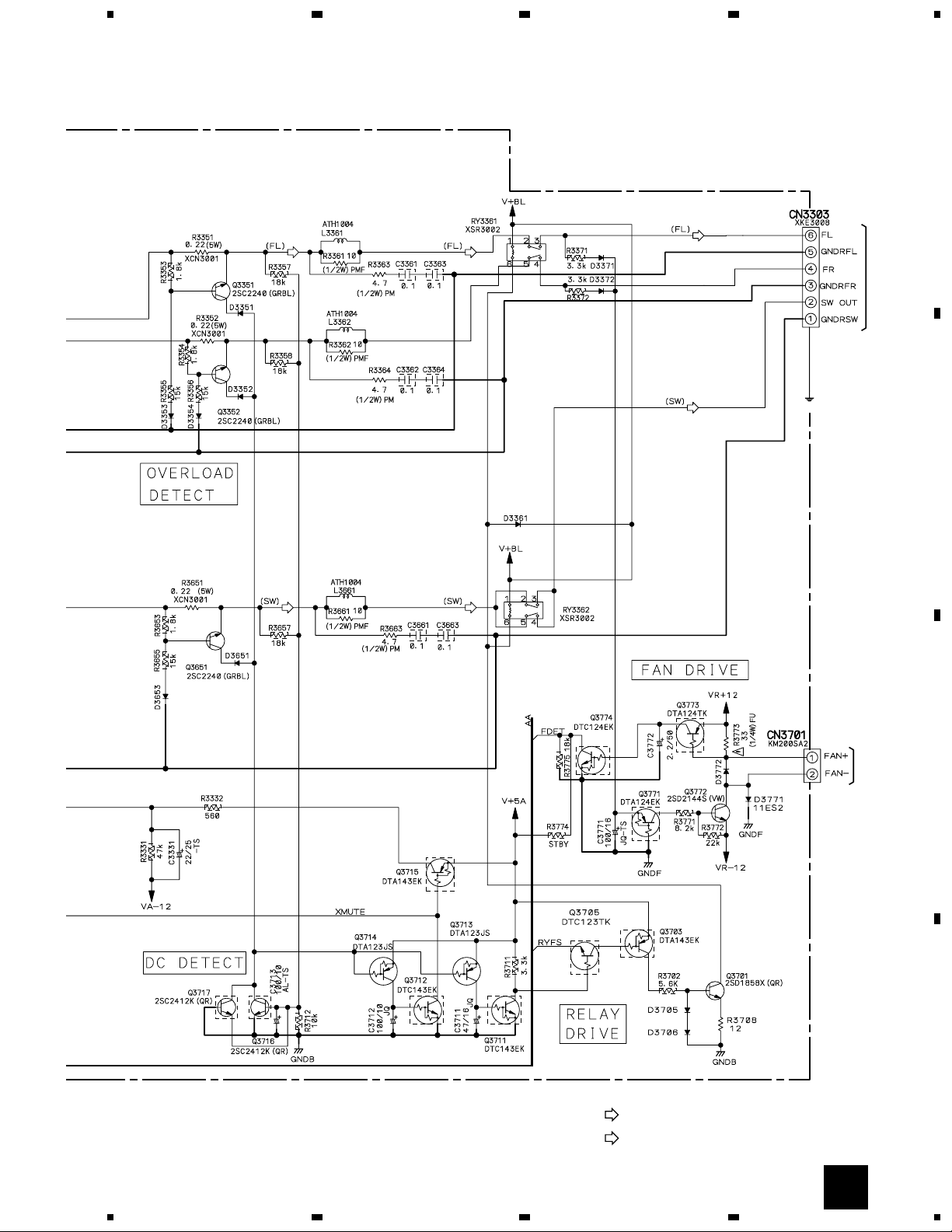
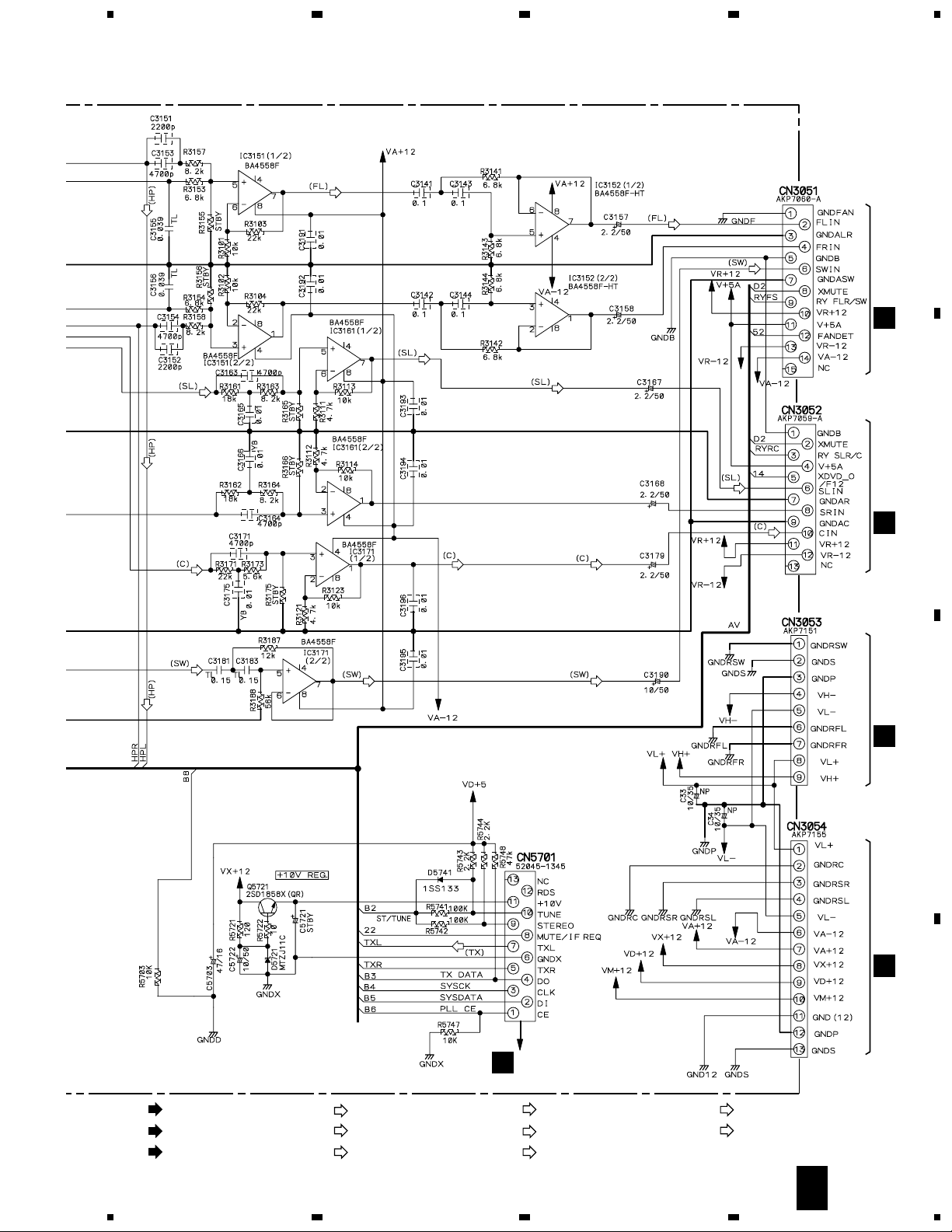
3.7 FRONT AMP ASSY
A
CN3051
G
I 2/3
B
23
FRONT AMP ASSY (XWZ3438)
4
CN3053
I 2/3
C
D
22
: The power supply is shown with the marked box.
G
1234
Page 23
5
678
XV-HTD510, XV-HTD510-B
A
SPEAKERS
B
C
DC FAN MOTOR
D
(FL)
: FL AUDIO SIGNAL ROUTE
(SW)
: SW AUDIO SIGNAL ROUTE
G
5
6
7
8
23
Page 24
1
XV-HTD510, XV-HTD510-B
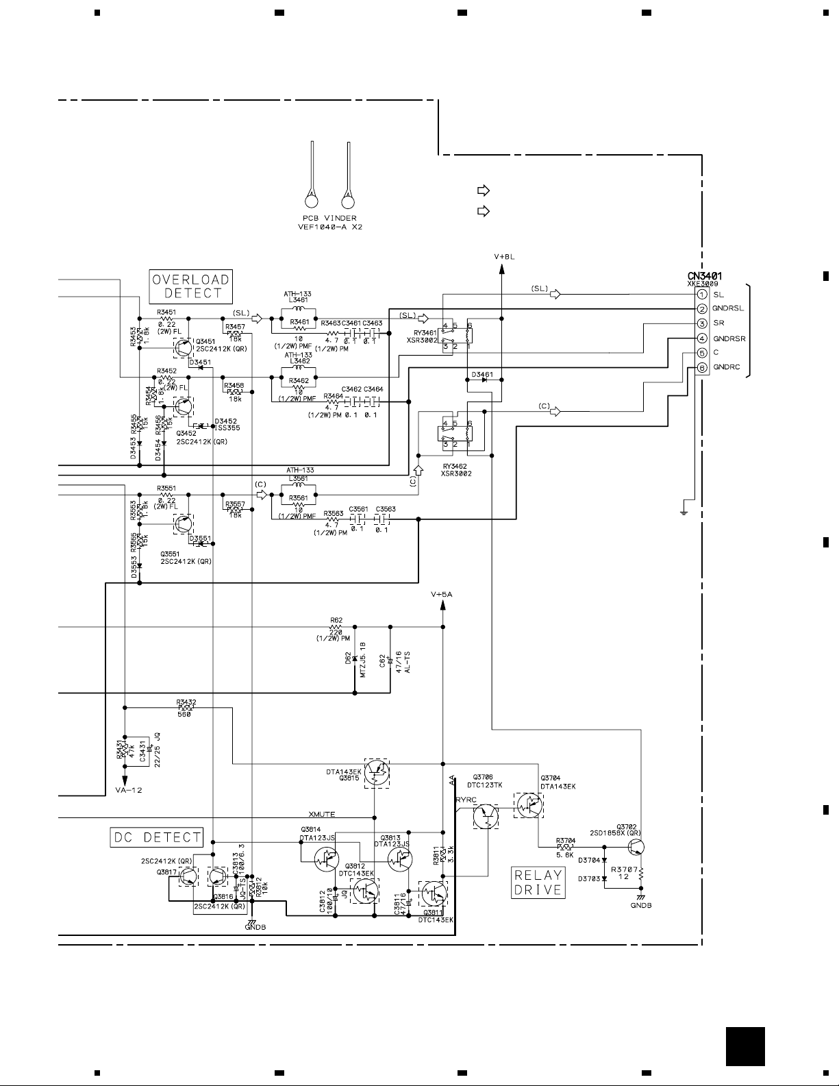
3.8 REAR AMP ASSY
A
CN3052
H
I 2/3
B
23
REAR AMP ASSY (XWZ3442)
4
CN3054
I 2/3
C
D
: The power supply is shown with the marked box.
24
H
1234
Page 25
5
678
XV-HTD510, XV-HTD510-B
A
(SL)
: SL AUDIO SIGNAL ROUTE
(C)
: C AUDIO SIGNAL ROUTE
SPEAKERS
B
C
D
H
5
6
7
8
25
Page 26
1
XV-HTD510, XV-HTD510-B
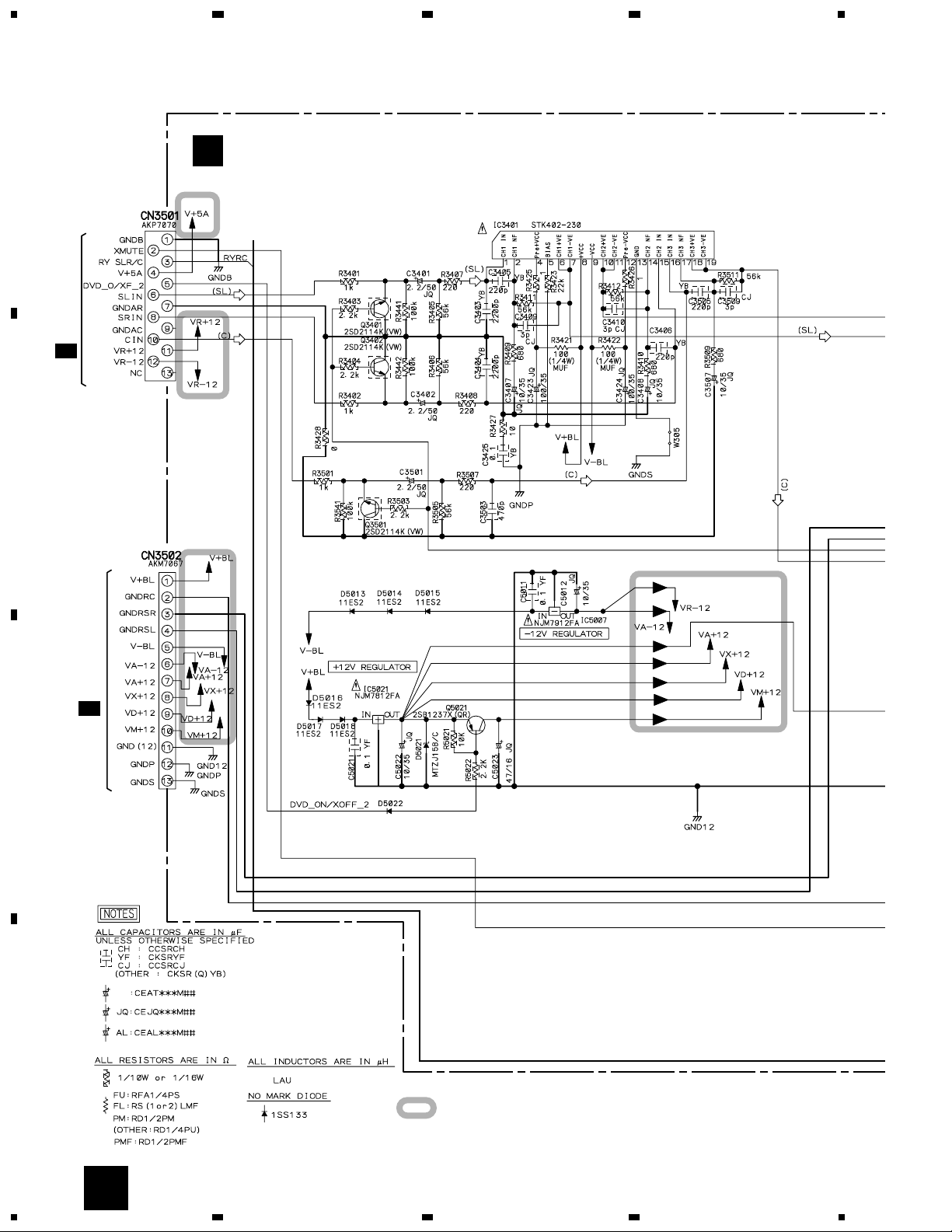
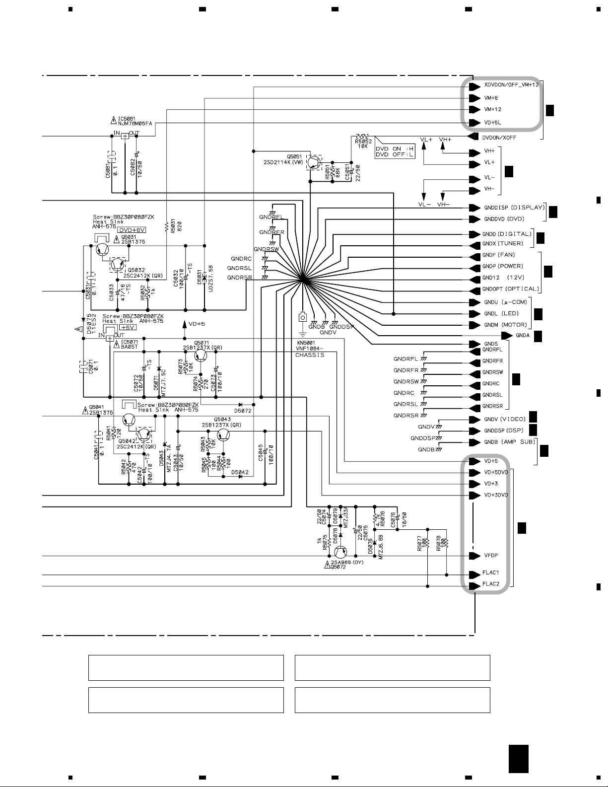
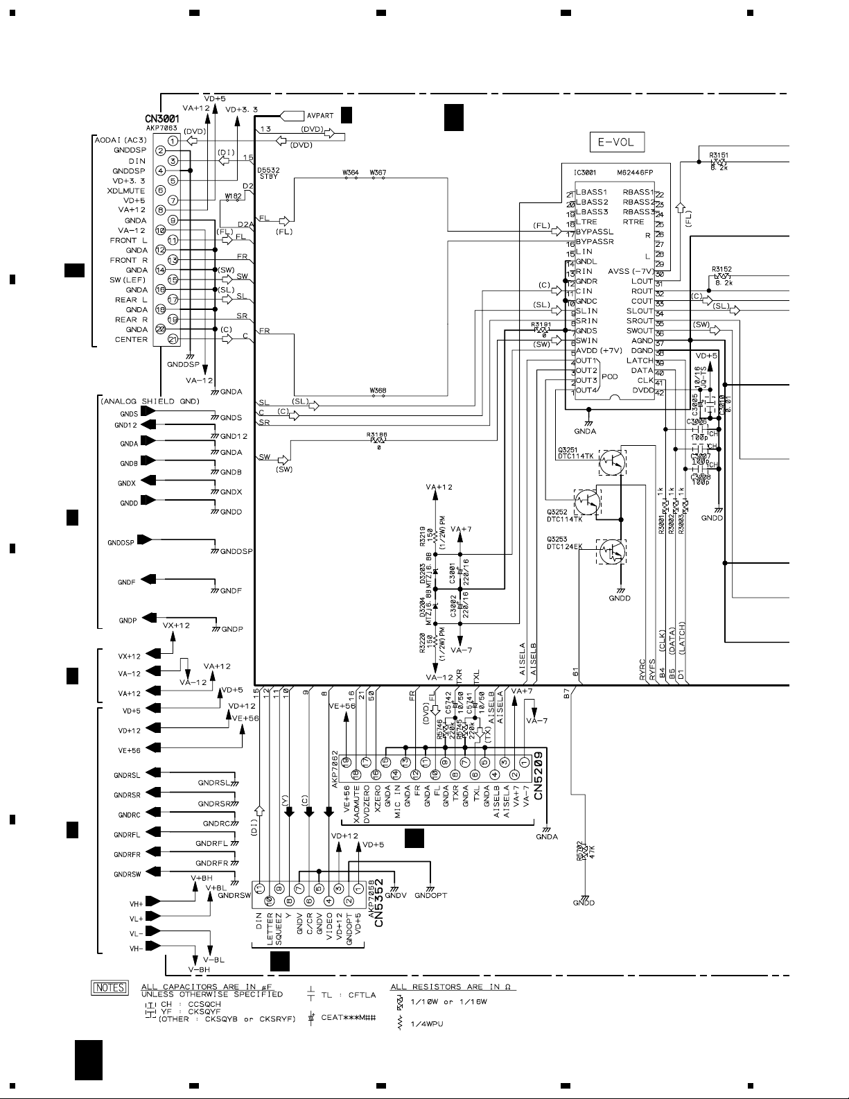
3.9 MAIN ASSY (1/3)
23
4
A
B
I 1/3
MAIN ASSY (XWX3030)
C
D
: The power supply is shown with the marked box.
26
1/3
I
1234
Page 27
5
678
XV-HTD510, XV-HTD510-B
I
3/3
I
2/3
I
3/3
I
2/3, 3/3
I
2/3
I
3/3
I
2/3, 3/3
I
2/3
A
B
CAUTION : FOR CONTINUED PROTECTION AGAINST RISK OF FIRE.
REPLACE ONLY WITH SAME TYPE NO. 491010 MFD, BY
LITTELFUSE INC. FOR IC13 AND IC14 (AEK7022).
CAUTION : FOR CONTINUED PROTECTION AGAINST RISK OF FIRE.
REPLACE ONLY WITH SAME TYPE NO. 491005 MFD, BY
LITTELFUSE INC. FOR IC15 AND IC5004 (AEK7019).
CAUTION : FOR CONTINUED PROTECTION AGAINST RISK OF FIRE.
REPLACE ONLY WITH SAME TYPE NO. 4910.75 MFD, BY
LITTELFUSE INC. FOR IC5001 (AEK7007).
CAUTION : FOR CONTINUED PROTECTION AGAINST RISK OF FIRE.
REPLACE ONLY WITH SAME TYPE NO. 49103.5 MFD, BY
LITTELFUSE INC. FOR IC5005 (AEK7017).
I
I
3/3
I
2/3, 3/3
3/3
I
2/3
C
D
1/3
I
5
6
7
8
27
Page 28
1
XV-HTD510, XV-HTD510-B
3.10 MAIN ASSY (2/3)
A
CN3702
M1/2
B
23
I
3/3
I 2/3
MAIN ASSY (XWX3030)
4
I
1/3
I
C
3/3
(VCB)
I
1/3
K
CN5208
D
28
2/3
I
1234
L
CN5351
Page 29
5
678
XV-HTD510, XV-HTD510-B
A
CN3301
G
B
CN3501
H
CN3302
G
C
CN3502
H
(VCB)
: VCB SIGNAL ROUTE
(Y)
: Y SIGNAL ROUTE
(C)
: C SIGNAL ROUTE
CN201
J
(DVD)
: DVD AUDIO SIGNAL ROUTE
(DI)
: DI AUDIO SIGNAL ROUTE
(FL)
: FL AUDIO SIGNAL ROUTE
5
6
(HP)
: HP AUDIO SIGNAL ROUTE
(SL)
: SL AUDIO SIGNAL ROUTE
(C)
: C AUDIO SIGNAL ROUTE
7
(SW)
: SW AUDIO SIGNAL ROUTE
(TX)
: TX AUDIO SIGNAL ROUTE
I
2/3
8
29
D
Page 30
1
XV-HTD510, XV-HTD510-B
23
4
3.11 MAIN ASSY (3/3)
I 3/3
A
CN15
MAIN ASSY (XWX3030)
F 3/3
B
(VCB)
I
1/3
I
2/3
I
I
2/3
1/3
I
2/3
I
1/3
I
1/3
C
CN5
F 2/3
I
1/3
D
30
T
N
N
CN5801
3/3
I
1234
CN5802
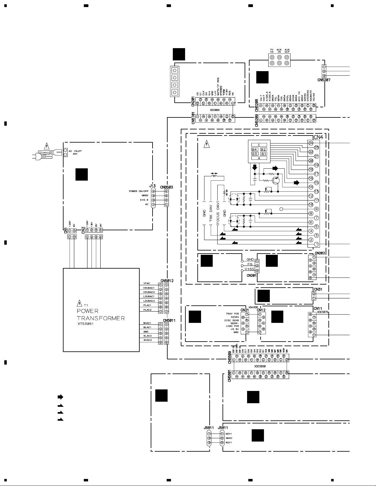
J13
Page 31

5
678
XV-HTD510, XV-HTD510-B
A
O
CN5807
3.1V
3.1V
0V
2.5V
2.5V
2.5V
LEVEL SHIFT
1.6V
1.6V
0V
0V
F 1/3
CN55
A
CN11
B
CN3701
C
M1/2
FOR DOWNLOAD
(VCB)
: VCB SIGNAL ROUTE
(Y)
: Y SIGNAL ROUTE
(C)
: C SIGNAL ROUTE
5
6
(DVD)
: DVD AUDIO SIGNAL ROUTE
(HP)
: HP AUDIO SIGNAL ROUTE
(T)
: TRAY POSITION SERVO LOOP LINE
(S)
: SEDO SERVO LOOP LINE
7
I
3/3
8
31
D
Page 32

1
XV-HTD510, XV-HTD510-B
3.12 TUNER MODULE
A
TUNER MODULE (AXQ7228)
J
FM FRONT END
23
4
B
(FM) (FM)
(FM)
(AM)
C
(AM)
(FM)
AM RF TUNING BLOCK
(AM)
(FM)
(AM) (AM)
OSC : 981 - 2052kHz 9k step
(FM)
(FM)
(FM)
(FM) (FM)
(AM)
D
32
J
1234
Page 33

5
678
XV-HTD510, XV-HTD510-B
A
: The power supply is shown with the marked box.
(TX)
: TUNER AUDIO SIGNAL ROUTE
(AM)
: AM SIGNAL ROUTE
(FM)
: FM SIGNAL ROUTE
(AM)
(FM)
(AM)
(AM)
(AM)
(AM)
(FM)
(AM)
(AM)
(FM)
(AM)
L201
ATE7003
(AM)
(FM)
(TX)
(TX)
(TX)
(TX)
(TX)
B
CN5701
2/3
I
C
D
J
5
6
7
8
33
Page 34

1
XV-HTD510, XV-HTD510-B
3.13 INPUT and VIDEO ASSYS
A
B
23
INPUT ASSY (XWZ3455)
K
4
C
VIDEO ASSY (XWZ3459)
L
D
34
K
L
1234
Page 35

5
678
XV-HTD510, XV-HTD510-B
A
M1/2
CN3703
I 2/3
CN5209
B
: The power supply is shown with the marked box.
(VCB)
(VCB)
(VCB)
(VCB)
(VCB)
I 2/3
CN5352
C
(VCB)
(VCB)
: VCB SIGNAL ROUTE
(Y)
: Y SIGNAL ROUTE
(C)
: C SIGNAL ROUTE
D
(DVD)
: DVD AUDIO SIGNAL ROUTE
(DI)
: DI AUDIO SIGNAL ROUTE
(FL)
: FL AUDIO SIGNAL ROUTE
5
6
(AI)
: AUX IN AUDIO SIGNAL ROUTE
(AO)
: AUX OUT AUDIO SIGNAL ROUTE
(TV)
: TV AUDIO SIGNAL ROUTE
7
(TX)
: TX AUDIO SIGNAL ROUTE
K
L
8
35
Page 36

1
XV-HTD510, XV-HTD510-B
3.14 DSP ASSY (1/2)
23
4
A
M 1/2
DSP ASSY (XWX3040)
I 3/3
CN5503
B
C
I 2/3
CN3001
D
36
K
CN5207
: The power supply is shown with the marked box.
1/2
M
1234
Page 37

5
678
XV-HTD510, XV-HTD510-B
A
M
2/2
B
(DVD)
: DVD AUDIO SIGNAL ROUTE
(DI)
: DI AUDIO SIGNAL ROUTE
(FL)
: FL AUDIO SIGNAL ROUTE
5
(SL)
: SL AUDIO SIGNAL ROUTE
(C)
: C AUDIO SIGNAL ROUTE
(SW)
: SW AUDIO SIGNAL ROUTE
6
: AUDIO SIGNAL ROUTE
7
M
2/2
M
M
2/2
1/2
8
C
D
37
Page 38

1
XV-HTD510, XV-HTD510-B
3.15 DSP ASSY (2/2)
M
1/2
A
(FL)
23
4
(FL)(FL)
M 2/2
B
(SL)
DSP ASSY (XWX3040)
(SL)(SL)
C
M
1/2
D
38
2/2
M
1234
(C)
(SW)
(C)(C)
(SW)(SW)
Page 39

5
678
XV-HTD510, XV-HTD510-B
(FL)
(FL)
(SL)(SL)
(FL)
: FL AUDIO SIGNAL ROUTE
(SL)
: SL AUDIO SIGNAL ROUTE
(C)
: C AUDIO SIGNAL ROUTE
(SW)
: SW AUDIO SIGNAL ROUTE
A
B
(C)
(SW)
(C)
(SW)
2/2
M
5
6
7
8
39
C
D
Page 40

1
23
XV-HTD510, XV-HTD510-B
3.16 DISPLAY, MIC HP, KEYB, STBY SWITCH, JOG and DISC KEY ASSYS
CN5509
I 3/3
A
B
I 3/3
4
CN5511
DISPLAY ASSY (XWZ3446)
N
C
D
DISC KEY ASSY (XWZ3449)
S
40
N
S
1234
Page 41

5
678
XV-HTD510, XV-HTD510-B
SWITCHES
JOG ASSY
S5801 : VOLUME
DISC KEY ASSY
S5803 : 0 OPEN/CLOSE
S5804 : EXCHANGE
S5805 : DISC SKIP
S5806 : 5
S5807 : 4
S5808 : 3
S5809 : 2
S5810 : 1
STBY SWITCH ASSY
S5811 : STANDBY/ON
O
DISC
MIC HP ASSY (XWZ3450)
A
KEYB ASSY
S5802 : ¡•¢ (FORWARD)
S5812 : DVD/CD
S5813 : TUNER/BAND
S5814 : TV/AUX
S5815 : CD MODE
S5816 : 7 (STOP)
S5817 : 6 (PLAY/PAUSE)
S5818 : 4•1 (REVERSE)
B
I 3/3
CN5501
JOG ASSY (XWZ3448)
R
5
KEYB ASSY (XWZ3447)
P
: The power supply is shown with the marked box.
6
N
7
STBY SWITCH ASSY
Q
(XWZ3453)
O
P
Q
R
8
C
D
41
Page 42

1
XV-HTD510, XV-HTD510-B
3.17 PRIMARY ASSY
A
I 1/3
B
CN5011
23
XTS3051
4
I 1/3
CN5012
C
I 3/3
CN8503
D
ATT7049
42
T
1234
Page 43

5
• NOTE FOR FUSE REPLACEMENT
CAUTION -
PRIMARY ASSY (XWZ3432)
T
FOR CONTINUED PROTECTION AGAINST RISK OF FIRE,
REPLACE WITH SAME TYPE AND RATINGS OF FUSE.
678
XV-HTD510, XV-HTD510-B
A
B
C
FU1: REK1067
5A
2.2M,1/2W
D
T
5
6
7
8
43
Page 44

1
23
XV-HTD510, XV-HTD510-B
WAVEFORMS
Note : The encircled numbers denote measuring point in the schematic diagram.
Measurement condition : No. 1 to 4 and 6 to 11 : MJK1, Title 1-chp 1
A
No. 5 : CD, ABEX-784 Track 1
No. 12 to 14 : MJK1, Title 1-chp 4
No. 15 to 17 : MJK1, Title 1-chp 5
4
Foot of R169 (RF)
1
V: 100mV/div. H: 0.2µsec/div.
TP2 (RFO)
2
V: 500mV/div. H: 0.1µsec/div.
GND
Foot of R261 (FPWM)
8
V: 1V/div. H: 5msec/div.
Foot of R262 (VPWM)
9
V: 1V/div. H: 5msec/div.
GND
IC18 - pin 36 (C output)
14
V: 0.2V/div. H: 5msec/div.
IC18 - pin 45 (CB output when
15
selecting color difference output)
V: 0.2V/div. H: 5msec/div.
GND
IC18 - pin 39 (Y output when
16
selecting color difference output)
V: 0.2V/div. H: 5msec/div.
IC18 - pin 36 (CR output when
17
selecting color difference output)
V: 0.2V/div. H: 5msec/div.
GND
B
TP3 (Tracking Error)
4
(AI-Inner Tracking Off)
V: 500mV/div. H: 2msec/div.
IC2 - pin 39 (EFM before slice)
5
V: 1V/div. H: 1µsec/div.
GND
Foot of R263 (PPWM)
10
V: 1V/div. H: 5msec/div.
Foot of R264 (RPWM)
11
V: 1V/div. H: 5msec/div.
GND
GND
CN55 - pin 5 (DISC SENS)
18
V: 2V/div. H: 1sec/div.
CN55 - pin 2 (TRAY POS)
19
V: 2V/div. H: 1sec/div.
18
GND
C
GND
GND
IC2 - pin 1 (EFM)
6
V: 1V/div. H: 0.2µsec/div.
IC3 - pin 41 (REGB)
7
V: 1V/div. H: 5msec/div.
GND
GND
IC18 - pin 45
12
(Composite Video output)
V: 0.2V/div. H: 1msec/div.
IC18 - pin 39 (Y output)
13
V: 0.2V/div. H: 5msec/div.
19
CN55 - pin 4 (SED0)
20
V: 2V/div. H: 5sec/div.
CLOSE
Tray Close
OPEN DISC CHANGE
GND
D
GND
GND
44
1234
Page 45

1
VOLTAGES
234
XV-HTD510, XV-HTD510-B
I 3/3
IC5501 (PDC076A)
Pin No. Voltage (V) Pin No. Voltage (V) Pin No. Voltage (V) Pin No. Voltage
MAIN ASSY
• Mode: DVD Play
1 4.8 26 2.4 51 -30.8 76 0
2 4.8 27 0 52 ∗ 77 0
3 3.3 28 0 53 ∗ 78 0
4 4.8 29 4.6 54 ∗ 79 4.7
5 4.8 30 ∗ 55 ∗ 80 −
6 4.8 31 ∗ 56 ∗ 81 4.7
7 4.8 32 ∗ 57 ∗ 82 4.5
8 4.8 33 ∗ 58 ∗ 83 0
9 3.3 34 ∗ 59 ∗ 84 4.7
10 3.4 35 ∗ 60 ∗ 85 0
11 4.8 36 ∗ 61 ∗ 86 0
12 0 37 ∗ 62 ∗ 87 4.8
13 3.2 38 ∗ 63 ∗ 88 0
14 0 39 ∗ 64 ∗ 89 0
15 2.5 40 ∗ 65 ∗ 90 4.8
16 2.5 41 ∗ 66 − 91 0
17 4.8 42 ∗ 67 0 92 0
18 4.8 43 − 68 5.0 93 0
19 4.9 44 − 69 4.2 94 0
20 0 45 − 70 0 95 0
21 0 46 4.8 71 0 96 0
22 4.8 47 ∗ 72 4.8 97 4.8
23 0.2 48 ∗ 73 4.9 98 0
24 4.7 49 ∗ 74 0 99 4.8
25 − 50 ∗ 75 0 100 4.6
A
B
C
Note ∗ : FL drive voltage, pulse waveform of Low level is VFDP (about -31V) and High level is VDD (+5V).
1
2
3
D
45
4
Page 46

1
23
XV-HTD510, XV-HTD510-B
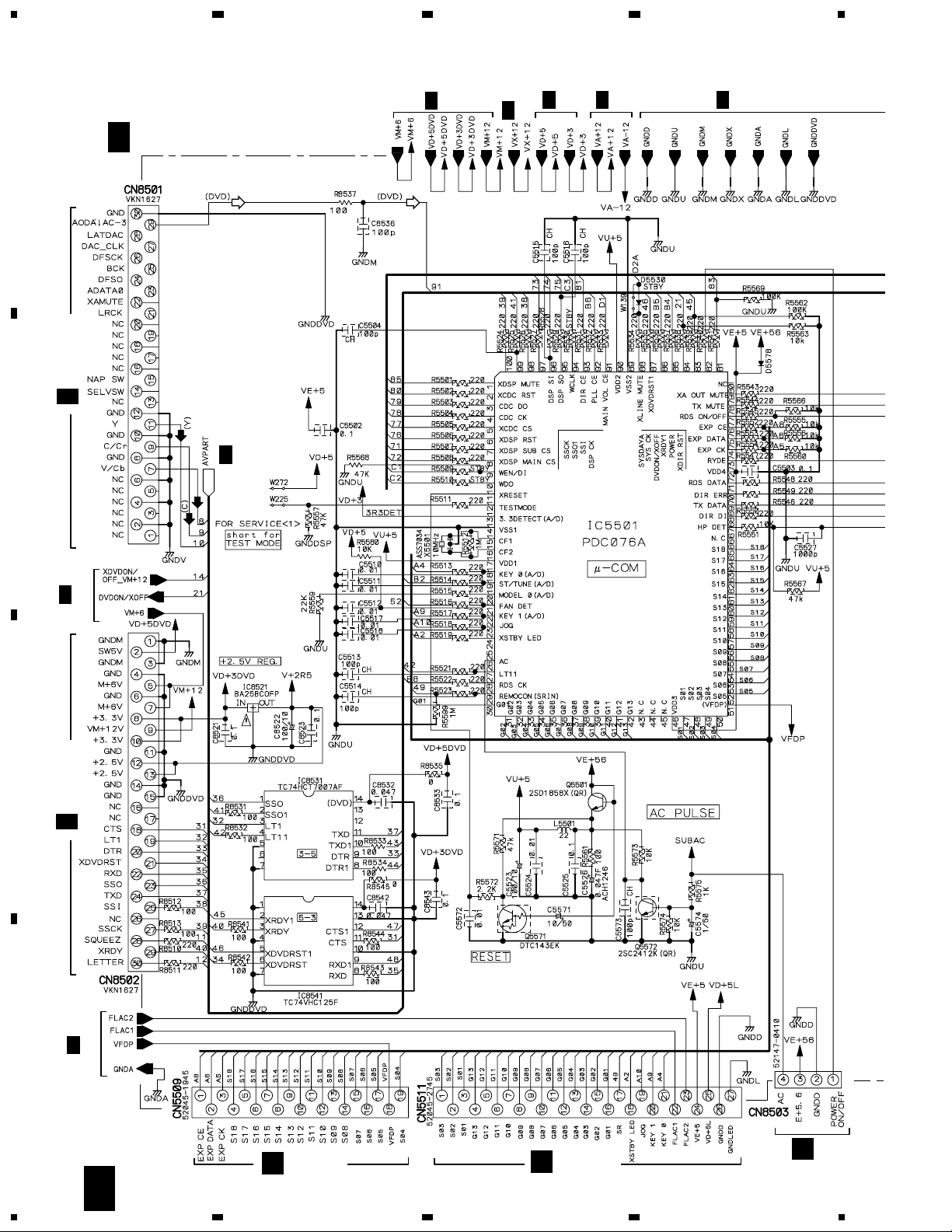
4. PCB CONNECTION DIAGRAM
A
NOTE FOR PCB DIAGRAMS :
1. Part numbers in PCB diagrams match those in the schematic
diagrams.
2. A comparison between the main parts of PCB and schematic
diagrams is shown below.
Symbol In PCB
Diagrams
BCE
BCE
D
B
Symbol In Schematic
Diagrams
BCEBCE
BCE
BCE
DGS
DGGSS
Part Name
Transistor
Transistor
with resistor
Field effect
transistor
Resistor array
3-terminal
regulator
3. The parts mounted on this PCB include all necessary parts for
several destinations.
For further information for respective destinations, be sure to
check with the schematic diagram.
4. View point of PCB diagrams.
Connector
Capacitor
SIDE A
P.C.Board
Chip Part
SIDE B
4
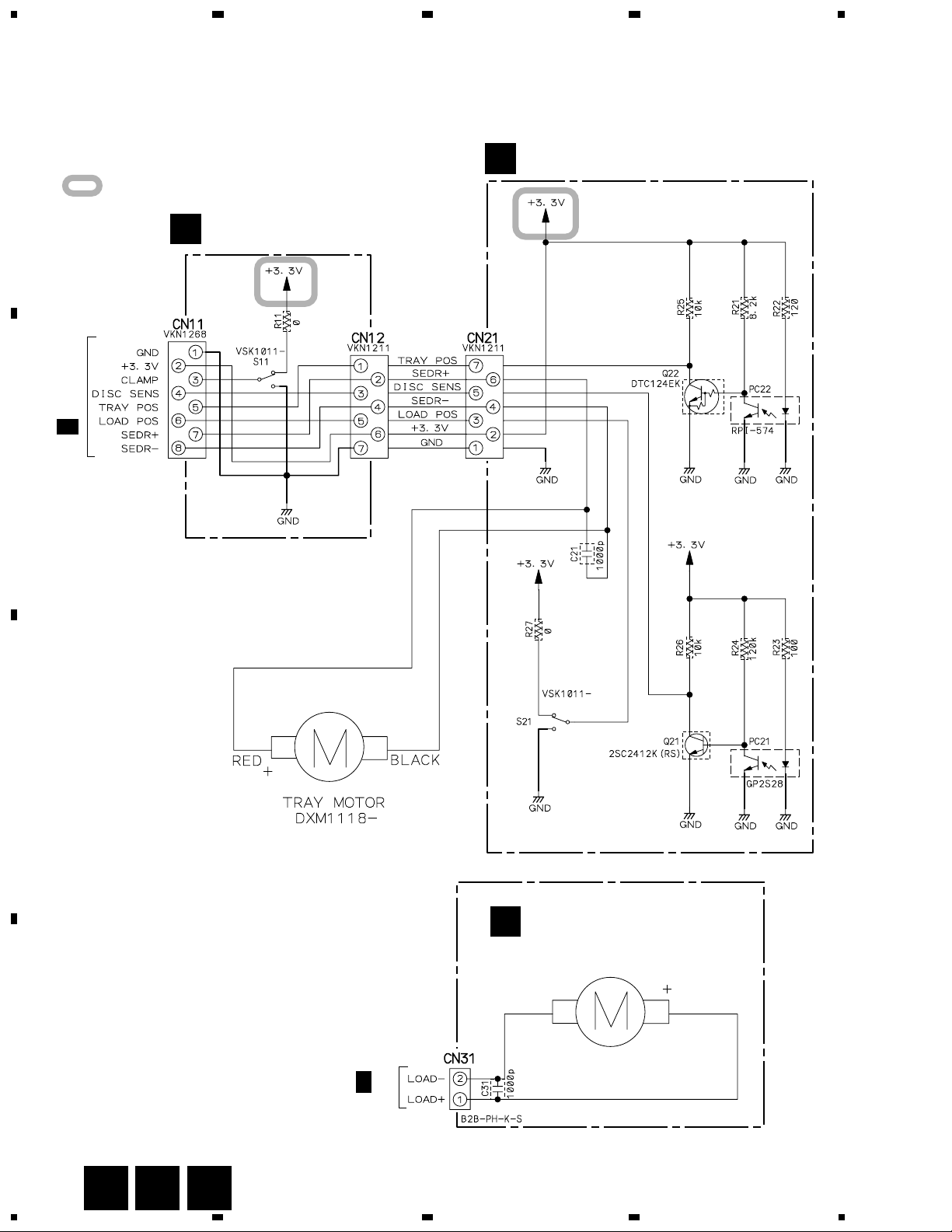
4.1 TRSB, SSRB, LOMB, SMEB and FGSB ASSYS
CN8903
TRSB ASSY
A
(XNP3042-A) (XNP3042-A)
C
(XNP3042-A)
SSRB ASSY
B
SMEB ASSY
D
I
CN2
F
M
C
LOADING
MOTOR
LOMB ASSY
CN3
F
TRSB ASSY
A
TRAY
M
MOTOR
(XNP3042-A)
SSRB ASSY
B
(XNP3042-A)(XNP3042-A)
SIDE B
E
FGSB ASSY
M
D
CARRIAGE
MOTOR
BLK
RED
(VNP1722-A)
M
SPINDLE
MOTOR
R101
PC101
(VNP1784-A)
SIDE A
46
A B C D E
1234
Page 47

1
4.2 TUNER MODULE
234
XV-HTD510, XV-HTD510-B
J
TUNER MODULE
SIDE A
A
B
J
TUNER MODULE
I
CN5701
Q202
(ANP7338-B)
SIDE B
C
D
Q201
1
2
IC201 Q205
3
Q203
IC202
(ANP7338-B)
Q204
J
4
47
Page 48

1
XV-HTD510, XV-HTD510-B
4.3 DVDM ASSY
A
23
4
F
DVDM ASSY
Q3
IC23
IC7 IC5
B
Q7
IC8
IC11
IC15
Q101Q121
Q6
SIDE A
IC21 Q4
Q103
Q5 Q102
C
PICKUP ASSY
IC1
IC18
Q109
Q107
Q81 IC3
Q83Q91
D
48
(VNP1817-A)
CN8902
I
F
1234
Page 49

1
234
XV-HTD510, XV-HTD510-B
A
C
CN31
SIDE B
CN8502
I
F
DVDM ASSY
Q1
IC14IC13IC12
B
Q112
CN202
D
IC2
IC19
Q114
Q113
Q131
Q106
IC26 IC27
Q251
Q85 Q89 Q87
C
D
CN8501
I
1
2
3
(VNP1817-A)
F
4
49
Page 50

1
XV-HTD510, XV-HTD510-B
4.4 FRONT AMP ASSY
A
B
I
CN3051
23
FRONT AMP ASSY
G
4
Q3701
C
D
I
CN3053
(XNP3044-C)
Q3714
Q3713
IC3301
IC3321
Q3351
Q3352
Q3651
Q3372
50
DC FAN MOTOR
SIDE A
G
1234
Page 51

1
FRONT AMP ASSY
G
234
XV-HTD510, XV-HTD510-B
A
Q3703
Q3705
Q3715
B
Q3603
Q3302
Q3301
Q3711
Q3712
Q3717
Q3716
C
Q3773
Q3771
Q3774
(XNP3044-C)
D
SIDE B
G
1
2
3
4
51
Page 52

1
XV-HTD510, XV-HTD510-B
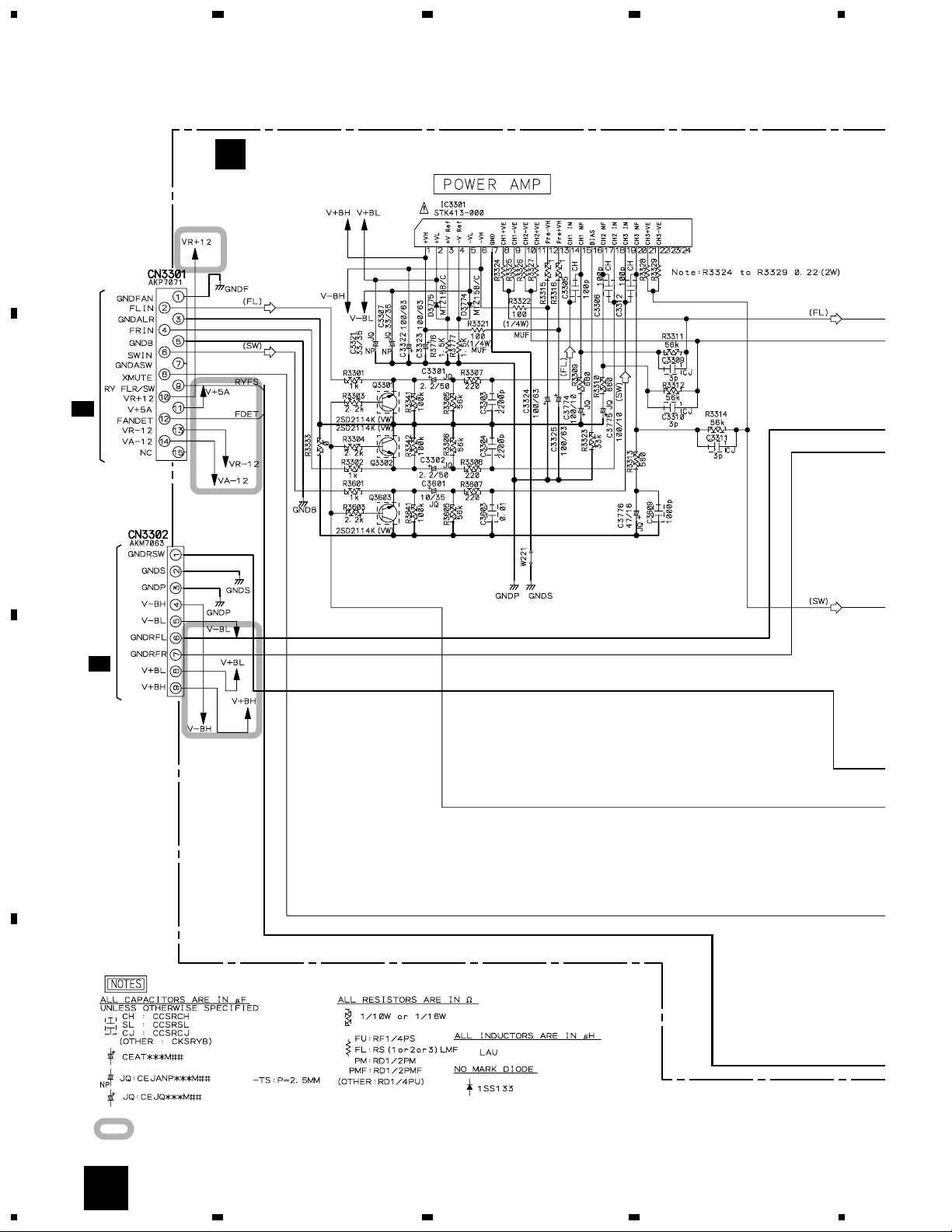
4.5 REAR AMP ASSY
A
Q3813
Q3702
Q3814
IC3322
B
IC3401
23
REAR AMP ASSY
H
4
I
CN3052
IC5021
I
CN3054
C
D
IC5007
Q5021
(XNP3044-C)
52
SIDE A
H
1234
Page 53

Q3816
Q3817
Q3811
Q3704
Q3706
Q3812
Q3452
Q3815
Q3451
1
234
XV-HTD510, XV-HTD510-B
A
REAR AMP ASSY
H
B
Q3551
Q3501
Q3401
Q3402
C
D
(XNP3044-C)
SIDE B
H
1
2
3
4
53
Page 54

1
T
XV-HTD510, XV-HTD510-B
4.6 MAIN ASSY
23
4
A
B
G
CN3301
H
CN3501
M
CN3702
MAIN ASSY
I
G
CN3302
H
CN3502
M
CN3701
C
D
L
CN5351
K
CN5208
54
CN201
J
IC3151 IC3152
I
1234
IC3002
IC3171 IC3161
IC3181
Q5721 IC15
CN5807
O
IC14
IC13 IC18
Page 55

5
678
XV-HTD510, XV-HTD510-B
N3701
F
CN15
F
CN55
A
CN11
F
CN5
A
B
IC17
N
CN5802
C
N
CN5801
D
SIDE A
Q5041
(XNP3043-C)
55
I
8
T
Q5072
5
IC5001 IC5004 IC5005
T1T1 J13
Q5071Q5501 IC5081 Q5043
IC5071
6
Q5031
7
Page 56

1
MAIN ASSY
I
IC8541 IC8531 IC8901 IC5401IC8521
IC5081
IC5501
Q5042 Q5032
Q5551-Q5554
Q5571Q5572
Q3905
Q3906
XV-HTD510, XV-HTD510-B
A
B
23
4
C
D
56
I
1234
Page 57

5
678
XV-HTD510, XV-HTD510-B
A
B
C
D
SIDE B
IC8802 Q3252Q3251 Q3253 IC3001
5
6
IC5701 Q3919Q3904 Q3903
7
(XNP3043-C)
57
I
8
Page 58

1
23
XV-HTD510, XV-HTD510-B
4.7 INPUT and VIDEO ASSYS
4
A
B
I
CN5209
INPUT ASSY
K
M
CN3703
INPUT ASSY
K
Q5272
Q5271
IC5353
IC5352
Q5273
Q5254
Q5231
IC5231
C
D
I
CN5352
VIDEO ASSY
L
VIDEO ASSY
L
Q5232
(XNP3048-C)(XNP3048-C)
IC5104
IC5351
Q5351
Q5181
Q5171
Q5161
58
K L
(XNP3048-C)(XNP3048-C)
SIDE A SIDE B
1234
Page 59

1
4.8 DSP ASSY
234
XV-HTD510, XV-HTD510-B
A
I
CN3001
DSP ASSY
M
Q8713
Q8718
Q8717
Q8716
IC8701
Q8710
Q8709
DSP ASSY
M
Q8711
Q8712
Q8714
Q8715
IC8703
IC8705
B
K
CN5207
I
CN5503
IC8801
IC3751
IC3801
IC3851
(XNP3045-C) (XNP3045-C)
C
D
SIDE A SIDE B
M
1
2
3
4
59
Page 60

1
23
XV-HTD510, XV-HTD510-B
4.9 DISPLAY, MIC HP, KEYB, STBY SWITCH, JOG and DISC KEY ASSYS
A
DISPLAY ASSY
N
B
4
CN5509
I
KEYB ASSY
P
(XNP3044-C)
C
MIC HP ASSY
O
I
CN5501
(XNP3044-C)
D
STBY SWITCH
Q
ASSY
60
N O P Q
1234
Page 61

5
678
XV-HTD510, XV-HTD510-B
A
509 CN5511
I
(XNP3044-C)
JOG ASSY
R
B
DISC KEY ASSY
S
(XNP3044-C)
SIDE A
(XNP3044-C)
C
(XNP3044-C)
D
N P R S
5
6
7
8
61
Page 62

1
XV-HTD510, XV-HTD510-B
A
23
DISPLAY ASSY
N
4
IC5801 Q5804
B
C
JOG ASSY
R
(XNP3044-C)
DISC KEY ASSY
S
KEYB ASSY
P
Q5803
(XNP3044-C)
D
SIDE B
62
N P R S
1234
Page 63

5
678
XV-HTD510, XV-HTD510-B
A
(XNP3044-C)
Q5802
B
MIC HP ASSY
O
IC5802
(XNP3044-C)
STBY SWITCH
Q
ASSY
(XNP3044-C)
(XNP3044-C)
C
D
N O P Q
5
6
7
8
63
Page 64

1
XV-HTD510, XV-HTD510-B
4.10 PRIMARY ASSY
A
AC IN
B
23
PRIMARY ASSY
T
4
T1
C
IC41
Q41
I
CN8503
(XNP3044-C)
D
SIDE A
64
T
1234
Page 65

1
PRIMARY ASSY
T
234
XV-HTD510, XV-HTD510-B
A
B
C
(XNP3044-C)
D
SIDE B
T
1
2
3
4
65
Page 66

XV-HTD510, XV-HTD510-B
Mark No. Description Part No. Mark No. Description Part No.
5. PCB PARTS LIST
NOTES:•Parts marked by "NSP" are generally unavailable because they are not in our Master Spare Parts List.
The mark found on some component parts indicates the importance of the safety factor of the part.
•
Therefore, when replacing, be sure to use parts of identical designation.
When ordering resistors, first convert resistance values into code form as shown in the following examples.
•
Ex.1 When there are 2 effective digits (any digit apart from 0), such as 560 ohm and 47k ohm (tolerance is shown by J=5%,
and K=10%).
560 Ω→56 × 10
47k Ω→47 × 10
0.5 Ω→R50 ..................................................................................... RN2H
1 Ω→1R0 ..................................................................................... RS1P
Ex.2 When there are 3 effective digits (such as in high precision metal film resistors).
5.62k Ω→ 562 × 10
1
→ 561 ........................................................ RD1/4PU 5 6 1 J
3
→ 473 ........................................................ RD1/4PU 4 7 3 J
R 5 0
1 R 0
1
→ 5621 ...................................................... RN1/4PC 5 6 2 1 F
K
K
Mark No. Description Part No.
LIST OF ASSEMBLIES
NSP 5C MECH. BASE ASSY XXA3027
NSP MECB ASSY XWM3197
NSP TRSB ASSY XWZ3461
NSP SSRB ASSY XWZ3462
NSP LOMB ASSY XWZ3463
Traverse Mechanism Assy-S VXX2653
NSP SMEB ASSY VWG2048
NSP FGSB ASSY VWG2009
NSP COMPLEX ASSY XWM3187
PRIMARY ASSY XWZ3432
FRONT AMP ASSY XWZ3438
REAR AMP ASSY XWZ3442
DISPLAY ASSY XWZ3446
KEYB ASSY XWZ3447
NSP JOG ASSY XWZ3448
NSP DISC KEY ASSY XWZ3449
MIC HP ASSY XWZ3450
NSP STBY SWITCH ASSY XWZ3453
NSP CONNECT ASSY XWM3193
INPUT ASSY XWZ3455
VIDEO ASSY XWZ3459
DVDM ASSY XWX3034
MAIN ASSY XWX3030
DSP ASSY XWX3040
TUNER MODULE AXQ7228
Mark No. Description Part No.
SSRB ASSY
B
SEMICONDUCTORS
Q21 2SC2412K
Q22 DTC124EK
PC21 GP2S28
PC22 RPI-574
SWITCH
S21 VSK1011
CAPACITOR
C21 CKSQYB102K50
RESISTORS
All Resistors RS1/10S J
OTHERS
CN21 7P FFC CONNECTOR VKN1211
LOMB ASSY
C
CAPACITOR
C31 CKSQYB102K50
TRSB ASSY
A
SWITCH
S11 VSK1011
RESISTORS
R11 RS1/10S0R0J
OTHERS
CN12 7P FFC CONNECTOR VKN1211
CN11 8P FFC CONNECTOR VKN1268
66
OTHERS
CN31 KR CONNECTOR B2B-PH-K
SMEB ASSY
D
SWITCH
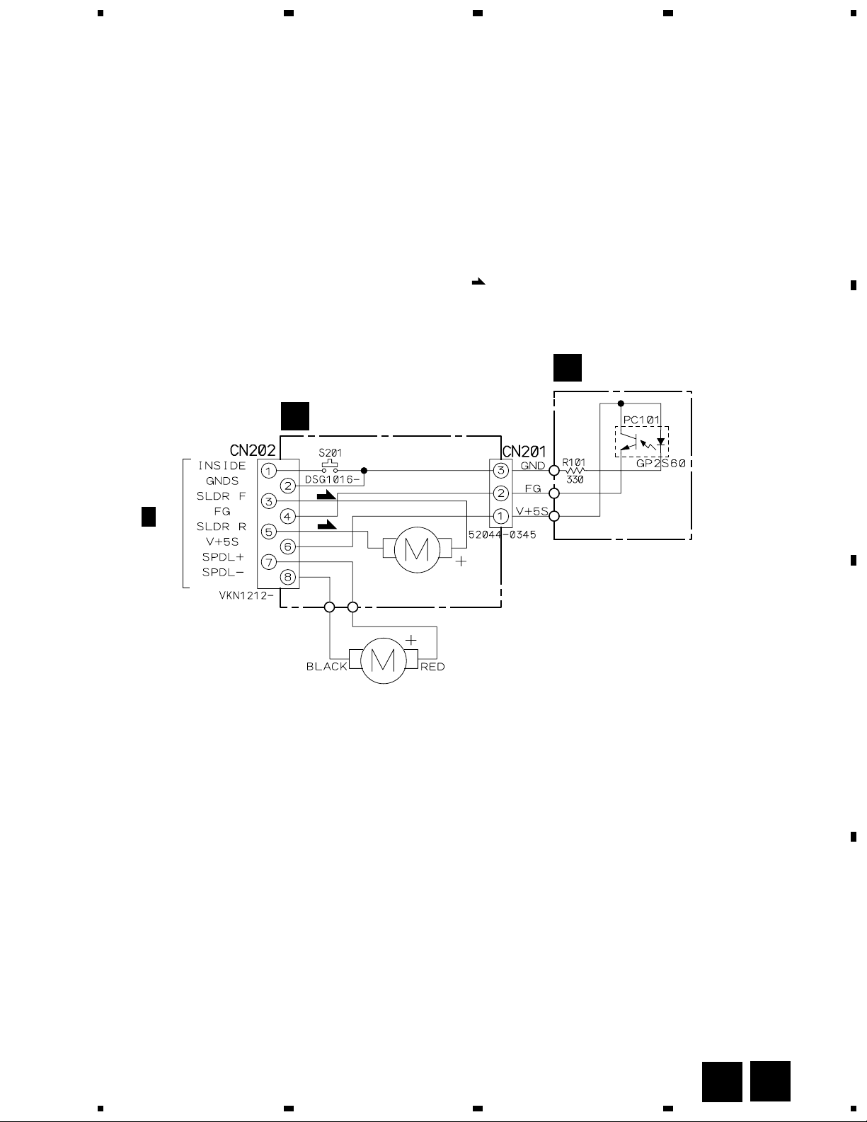
S201 DSG1016
OTHERS
CN201 3P FFC CONNECTOR 52044-0345
CN202 8P FFC CONNECTOR VKN1212
PC BOARD SMEB VNP1722
Page 67

XV-HTD510, XV-HTD510-B
Mark No. Description Part No. Mark No. Description Part No.
C124,C132 CCSRCH680J50
FGSB ASSY
E
SEMICONDUCTOR
PC101 GP2S60
C117,C240,C352,C360 CCSRCH681J25
C129,C142,C842 CEV101M10
C113,C139 CEV220M16
C405,C413,C700,C808 CEV221M4
RESISTOR
R101 RS1/10S331J
DVDM ASSY
F
SEMICONDUCTORS
IC5,IC7 BA4510F
IC21 BU2288FV
IC14 KM68V1000CLT-7L
IC1 LA9701M
IC2 LC78652W
IC3 M56788FP
IC19
IC18 MB86373B
IC15 MN414800CSJ-07
IC11 PD3410A
IC12 PE5108A
IC8 TC7SHU04F
IC13 XYW3003
Q106,Q109,Q81,Q83,Q85 2SA1576A
Q114,Q121,Q251 2SC4081
Q131 DTC114EUA
Q102 HN1A01F
Q103,Q6,Q7 HN1B04FU
Q101 HN1C01F
Q112,Q113 HN1C01FU
Q107,Q4,Q5 RN1902
Q3 RN1911
Q1 RN4982
D301 KV1471E
D6 RB501V-40
COILS
L150,L330 LCYA100J2520
L304 LCYA2R7J2520
L81 CHIP COIL VTL1067
L9170 CHIP BEAD VTL1084
CAPACITORS
C845,C846,C849-C852 CCSRCH100D50
C123,C146,C613,C806,C843 CCSRCH101J50
C372,C402,C404,C408 CCSRCH101J50
C322 CCSRCH120J50
C135 CCSRCH121J50
C104-C108 CCSRCH150J50
C206,C210,C211 CCSRCH151J50
C333 CCSRCH180J50
C314,C336 CCSRCH220J50
C152 CCSRCH221J50
C151 CCSRCH270J50
C127,C209,C337 CCSRCH331J50
C116,C134,C236 CCSRCH470J50
C122,C208 CCSRCH471J50
C126,C335 CCSRCH560J50
C334 CCSRCH5R0C50
MB811171622A-100FN
C368,C411 CEV470M16
C111,C149,C205,C207,C401 CEV470M6R3
C403,C407 CEV470M6R3
C140,C223,C224,C252,C264 CKSQYB105K10
C312 CKSQYB105K10
C216,C313 CKSRYB102K50
C133,C136,C203,C220,C225 CKSRYB103K50
C239,C320,C321,C330,C625 CKSRYB103K50
C703,C711 CKSRYB103K50
C101,C102,C114,C118,C119 CKSRYB104K25
C121,C138,C204,C212,C213 CKSRYB104K25
C227,C231,C263,C315,C317 CKSRYB104K25
C332,C804,C604,C606,C609 CKSRYB104K25
C611,C612,C614,C617,C619 CKSRYB104K25
C705,C707,C709,C710,C713 CKSRYB104K25
C714,C722,C724,C807,C809 CKSRYB104K25
C811,C812,C814,C815,C817 CKSRYB104K25
C819,C821 CKSRYB104K25
C153,C266,C357 CKSRYB223K50
C214,C251,C261,C351,C354 CKSRYB472K50
C109,C110,C120,C130,C131 CKSRYF104Z50
C143,C150,C1901,C1902,C202 CKSRYF104Z50
C215,C221,C222,C226,C230 CKSRYF104Z50
C235,C265,C299,C319,C359 CKSRYF104Z50
C367,C369,C370,C601,C605 CKSRYF104Z50
C607,C608,C610,C615,C618 CKSRYF104Z50
C620,C626,C701,C702,C704 CKSRYF104Z50
C706,C708,C712,C715-C721 CKSRYF104Z50
C723,C726,C820,C844 CKSRYF104Z50
C148,C217,C327,C801,C802 CKSRYF105Z10
C810,C813,C818,C828,C830 CKSRYF105Z10
RESISTORS
R632 RAB4C0R0J
R657,R658 RAB4C103J
R121,R663 RAB4C220J
R123 RAB4C390J
R202,R3510 RS1/10S101J
R700 RS1/10S1R0J
R807 RS1/16S1201F
R806 RS1/16S1501F
R363,R365 RS1/16S1503F
R825-R827 RS1/16S2000F
R805 RS1/16S2701F
R361,R364 RS1/16S7502F
Other Resistors RS1/16S J
OTHERS
X2 CHIP CERALOCK DSS1110
CN2 PH CONNECTOR S2B-PH-SM3
CN555 24P FFC CONNECTOR VKN1464
CN55 7P FFC CONNECTOR VKN1493
CN15,CN5
CN3 8P FFC CONNECTOR VKN1763
X1
(20MHz)
FLEXIBLE CABLE(07P) VDA1681
B TO B CONNECTOR 30P
CRYSTAL RESONATOR
(27.000MHz)
VKN1626
VSS1159
67
Page 68

XV-HTD510, XV-HTD510-B
Mark No. Description Part No. Mark No. Description Part No.
FRONT AMP ASSY
G
SEMICONDUCTORS
IC3301 STK413-000
Q3351,Q3352,Q3651 2SC2240
Q3716,Q3717 2SC2412K
Q3701 2SD1858X
Q3301,Q3302,Q3603 2SD2114K
Q3772 2SD2144S
Q3713,Q3714 DTA123JS
Q3771 DTA124EK
Q3773 DTA124TK
Q3703,Q3715 DTA143EK
Q3705 DTC123TK
Q3774 DTC124EK
Q3711,Q3712 DTC143EK
D3771 11ES2
D3351-D3354,D3361,D3371,D3372 1SS133
D3651,D3653,D3705,D3706,D3772 1SS133
D3774,D3775 MTZJ15B
COILS
L3361,L3362,L3661 ATH1004
RELAYS
RY3361,RY3362 XSR3002
CAPACITORS
C3305,C3306,C3312 CCSRCH101J50
C3309-C3311 CCSRCJ3R0C50
C3713 CEAL101M10
C3771 CEAT101M16
C3322-C3325 CEAT101M63
REAR AMP ASSY
H
SEMICONDUCTORS
IC5021 NJM7812FA
IC5007 NJM7912FA
IC3401 STK402-230
Q5021 2SB1237X
Q3451,Q3452,Q3551,Q3816,Q3817 2SC2412K
Q3702 2SD1858X
Q3401,Q3402,Q3501 2SD2114K
Q3813,Q3814 DTA123JS
Q3704,Q3815 DTA143EK
Q3706 DTC123TK
Q3811,Q3812 DTC143EK
D5013-D5018 11ES2
D3451,D3453,D3454,D3461,D3551 1SS133
D3553,D3703,D3704,D5022 1SS133
D3452 1SS355
D5021 MTZJ15B
D62 MTZJ5.1B
COILS
L3461,L3462,L3561 ATH-133
RELAYS
RY3461,RY3462 XSR3002
CAPACITORS
C3409,C3410,C3509 CCSRCH330J50
C62 CEAL470M16
C3811 CEAT470M16
C3407,C3408,C3507,C5012,C5022 CEJQ100M35
C3812 CEJQ101M10
C3772 CEAT2R2M50
C3601 CEJQ100M35
C3712,C3774,C3775 CEJQ101M10
C3331 CEJQ220M25
C3301,C3302 CEJQ2R2M50
C3711,C3776 CEJQ470M16
C3307,C3321 CEJQNP330M35
C3609 CKSRYB102K50
C3603 CKSRYB103K50
C3361-C3364,C3661,C3663 CKSRYB104K25
C3303,C3304 CKSRYB222K50
RESISTORS
R3363,R3364,R3663 RD1/2PM4R7J
R3361,R3362,R3661 RD1/2PMF100J
R3321,R3322 RD1/4MUF101J
R3708 RD1/4PU120J
R3776,R3777 RD1/4PU152J
R3773 RF1/4PS330J
R3324-R3329 RS2LMFR22J
R3351,R3352,R3651 (0.22Ω/5W) XCN3001
Other Resistors RS1/16S J
OTHERS
CN3302 09P CONNECTOR PLUG AKM7063
CN3301 15P SOCKET AKP7071
CN3701 PLUG(2P) KM200SA2
CN3303 SPEAKER TERMINAL 6-P XKE3008
C3423,C3424 CEJQ101M35
C3813 CEJQ101M6R3
C3431 CEJQ220M25
C3401,C3402,C3501 CEJQ2R2M50
C5023 CEJQ470M16
C3425,C3461-C3464,C3561,C3563 CKSRYB104K25
C3405,C3406,C3505 CKSRYB221K50
C3403,C3404,C3503 CKSRYB471K50
C5011,C5021 CKSRYF104Z50
RESISTORS
R62 RD1/2PM221J
R3463,R3464,R3563 RD1/2PM4R7J
R3461,R3462,R3561 RD1/2PMF100J
R3421,R3422 RD1/4MUF101J
R3707 RD1/4PU120J
R3451,R3452,R3551 RS2LMFR22J
Other Resistors RS1/16S J
OTHERS
CN3502 13P CONNECTOR PLUG AKM7067
CN3501 13P SOCKET AKP7070
PCB BINDER VEF1040
CN3401 SPEAKER TERMINAL 6P XKE3009
68
Page 69

XV-HTD510, XV-HTD510-B
Mark No. Description Part No. Mark No. Description Part No.
C3157,C3158,C3167,C3168,C3179 CEAT2R2M50
MAIN ASSY
I
SEMICONDUCTORS
IC5001 PROTECTOR (750mA) AEK7007
IC5005 PROTECTOR (3.5A) AEK7017
IC15,IC5004 PROTECTOR (5A) AEK7019
IC13,IC14 PROTECTOR (10A) AEK7022
IC5071 BA05T
C5006,C5008 CEAT682M16
C5033,C5703 CEAT470M16
C31,C32 CEAT472M35
C3005 CEJQ100M16
C3181,C3183 CFTLA154J50
C3155,C3156 CFTLA393J50
C3913,C3914,C5527 CKSRYB102K50
IC8521 BA25BC0FP
IC3151,IC3152,IC3161,IC3171 BA4558F
IC3902 BA4560F
IC8901 BA6195FP
IC3001 M62446FP
IC5081 NJM78M05FA
IC5501 PDC076A
IC8531 TC74HCT7007AF
IC8541 TC74VHC125F
Q3906 2SA1037K
Q5072 2SA965
Q5043,Q5071 2SB1237X
Q5031,Q5041 2SB1375
Q5032,Q5042,Q5572 2SC2412K
Q5501,Q5721 2SD1858X
Q3903,Q3904,Q3919,Q3920,Q5051 2SD2114K
Q3905 DTA124EK
Q5553,Q5554 DTA143EK
Q3251,Q3252 DTC114TK
Q8922 DTC114YK
Q3253 DTC124EK
Q5551,Q5552,Q5571 DTC143EK
D5010,D5011,D5074,D5075 11ES2
D3901,D5042,D5072,D5078,D5578 1SS133
D5741 1SS133
D5005,D5006 D3SBA20(B)
D11,D12 D5SBA20(B)
D5721 MTZJ11C
D5079 MTZJ33A
D5043 MTZJ4.7A
D3203,D3204,D5076 MTZJ6.8B
D5071 MTZJ7.5C
D5031 UDZS7.5B
COIL
L5501 LAU220J
CAPACITORS
C5526 (0.047F) ACH1246
C21,C22 (3300µF/56V) ACH7045
C3006-C3008,C5504,C5513-C5516 CCSRCH101J50
C5573,C8536,C8914 CCSRCH101J50
C8910-C8913,C8916 CCSRCH221J50
C9004 CCSRCH331J50
C8907 CEAL101M10
C33,C34 CEANP100M35
C3190,C3903-C3908,C3917,C5043 CEAT100M50
C5072,C5076,C5082,C5571,C5722 CEAT100M50
C5741,C5742 CEAT100M50
C5032,C5042,C5045,C5073,C5523 CEAT101M10
C8522,C8909 CEAT101M10
C5010 CEAT101M50
C5574 CEAT1R0M50
C5051,C5074,C5075 CEAT220M50
C3001,C3002 CEAT221M16
C3010,C3165,C3166,C3175 CKSRYB103K50
C3191-C3196,C5510-C5512 CKSRYB103K50
C5517,C5518,C5524,C5572,C8902 CKSRYB103K50
C8908,C9003 CKSRYB103K50
C3141-C3144,C5031,C5041,C5071 CKSRYB104K25
C5081,C5502,C5503,C5525,C8521 CKSRYB104K25
C8523,C8533,C8543,C8905,C8906 CKSRYB104K25
C8915 CKSRYB104K25
C3911,C3912 CKSRYB221K50
C3151,C3152 CKSRYB222K50
C3153,C3154,C3163,C3164,C3171 CKSRYB472K50
C8532,C8542 CKSRYB473K25
RESISTORS
R3219,R3220 RD1/2PM151J
R5077,R5078,R8533,R8534 RD1/4PU101J
R5075 RD1/4PU102J
R5580 RD1/4PU103J
R3909,R3910 RD1/4PU470J
R5076 RD1/4PU472J
R5568 RD1/4PU473J
R5031 RD1/4PU821J
R8930 RS1/16S1002F
R8909 RS1/16S1502F
R8914,R8928 RS1/16S2402F
R8927 RS1/16S2701F
R8929 RS1/16S5601F
Other Resistors RS1/16S J
OTHERS
CN5501 5P FFC CONNECTOR 52045-0545
CN5701 13P FFC CONNECTOR 52045-1345
CN5509 19P FFC CONNECTOR 52045-1945
CN5511 27P FFC CONNECTOR 52045-2745
CN8503
CN5352 11P PLUG AKP7058
CN3052 13P PLUG AKP7059
CN3051,CN5503 15P PLUG AKP7060
CN5209 19P PLUG AKP7062
CN3001 21P PLUG AKP7063
CN3053 09P CONNECTOR AKP7151
CN3054 13P CONNECTOR AKP7155
CN5011 5P-VH CONNECTOR B5P-VH
CN5012 7P-VH CONNECTOR B7P-VH
CN5507,CN8902 VKN1211
CN8501,CN8502 VKN1627
CN8903 8P FFC CONNECTOR VKN1707
KN5001 EARTH METAL FITTING VNF1084
X5501 CERAMIC RESONATOR ASS7034
4P JUMPER CONNECTOR
SOCKET
SOCKET
HEAT SINK ANH-575
SCREW BBZ30P080FZK
7P FFC CONNECTOR
B TO B CONNECTOR 30P
(10MHz)
52147-0410
69
Page 70

XV-HTD510, XV-HTD510-B
Mark No. Description Part No. Mark No. Description Part No.
TUNER MODULE
J
SEMICONDUCTORS
IC201 BA1451F
IC202 LC72131MD
Q201,Q204,Q205 2SC2412K
Q202 DTA124ES
Q203 DTC124EK
D201 1SS133
D202 MTZJ5.1C
COILS AND FILTERS
L201 ATE7003
F202 ATF-107
F201 ATF-119
F203 ATF1155
CAPACITORS
C206 CCSRCH100D50
C212,C213,C226,C233-C235 CCSRCH101J50
C240 CCSRCH101J50
C231,C232 CCSRCH150J50
C223 CEAT100M50
C229 CEAT101M10
C224 CEAT1R0M50
C227 CEAT220M25
C241 CEAT2R2M50
C243 CEAT330M16
C228 CEAT3R3M50
C237 CEAT470M10
C211 CEJA1R0M50
C210 CEJA470M16
C204,C238,C602 CKSRYB102K50
INPUT ASSY
K
SEMICONDUCTORS
IC5352 BA4558F-HT
IC5231 BU4052BCF
Q5271,Q5272 2SD2114K
Q5273 DTA124EK
Q5231,Q5232 DTC124EK
D5253 1SS181
D5252 1SS355
COILS
L5201,L5202,L5205,L5207,L5208 VTL1112
L5211,L5271,L5272,L5280 VTL1112
CAPACITORS
C5201-C5204,C5207-C5210 CCSRCH101J50
C5271,C5272 CCSRCH101J50
C5239,C5240 CEAT100M50
C5212-C5215,C5231,C5232 CEAT470M16
C5229,C5230,C5233,C5234 CKSRYB103K50
C5244-C5246 CKSRYB103K50
RESISTORS
Other Resistors RS1/16S J
OTHERS
JA5201 PIN JACK (6P) AKB7113
CN5208 19P SOCKET AKP7073
CN5207 KR CONNECTOR S3B-PH-K
C101,C102,C208,C220,C239 CKSRYB103K50
C242,C601 CKSRYB103K50
C216,C217 CKSRYB123K50
C225 CKSRYB153K50
C201,C205,C209,C214,C230 CKSRYB223K50
C236,C603 CKSRYB223K50
C221 CKSRYB224K10
C202,C222 CKSRYB473K16
C215 CKSRYB681K50
RESISTORS
R211 RD1/4PU221J
R221 RD1/4PU222J
R233 RD1/4PU391J
R243 RS1/10S0R0J
R103 RS1/10S331J
R104 RS1/10S391J
Other Resistors RS1/16S J
OTHERS
CN201 13P CONNECTOR 52044-1345
BN201 TERMINAL 4P AKA7003
X201 CRYSTAL RESONATOR ASS1093
SHIELD CASE T ANK7072
SHIELD CASE B ANK7073
(7.2000MHz)
FM FRONT END AXF7003
AM RF TUNING BLOCK AXX7071
VIDEO ASSY
L
SEMICONDUCTORS
IC5351 LA7138M
IC5104 TC7WU04F
Q5161,Q5171,Q5181,Q5351 2SA1037K
COILS AND FILTERS
L5161,L5171,L5181 LCTB120K1608
F5101 VTF1096
L5371,L5378,L5379 VTL1087
CAPACITORS
C5106 CCSRCH100D50
C5163,C5173,C5183 CCSRCH180J50
C5371,C5379 CCSRCH331J50
C5161,C5162,C5171,C5172 CCSRCH6R0D50
C5181,C5182 CCSRCH6R0D50
C5354,C5356,C5360 CEAT101M16
C5105 CEAT470M16
C5372,C5380 CEAT471M6R3
C5107,C5392 CKSRYB102K50
C5101,C5103,C5104,C5164,C5174 CKSRYB104K25
C5184,C5351-C5353,C5357,C5361 CKSRYB104K25
C5381 CKSRYB104K25
RESISTORS
Other Resistors RS1/16S J
70
Page 71

XV-HTD510, XV-HTD510-B
Mark No. Description Part No. Mark No. Description Part No.
OTHERS
JA5103 PIN JACK (1P) AKB7111
CN5352 4P MINI DIN SOCKET AKP7008
CN5351 11P SOCKET AKP7069
JA5351 PIN JACK (1P) VKB1063
DSP ASSY
M
SEMICONDUCTORS
IC3751 AK4527BVQ
IC8701,IC8703,IC8705 BA4558F-HT
IC8801 LC89056W-E
IC3851 W24257AJ-12
IC3801 YSS912C
Q8709-Q8714 2SD2114K
Q8715,Q8716,Q8718 DTA124EK
Q8717 DTC124EK
D8701,D8702 1SS181
D8703 1SS184
FILTERS
F3731-F3736,F3801,F3802,F3851 DTF1064
F8801,F8802 DTF1064
F3751,F3752 DTF1067
CAPACITORS
C3807,C3810,C3814,C3817,C3821 CCSRCH101J50
C3825,C3828,C3854,C8825 CCSRCH101J50
C8733 CCSRCH121J50
C3803,C3804,C8816,C8817 CCSRCH200J50
C3820 CCSRCH221J50
C8709,C8710 CCSRCH470J50
C3811 CCSRCH471J50
C8721,C8722 CCSRCH820J50
C8711,C8712,C8723,C8724 CEAT100M50
C8735,C8736,C8741-C8746 CEAT100M50
RESISTORS
R3751,R3757,R3809,R3813,R3822 RAB4C101J
R3827,R3830,R8801,R8825 RAB4C101J
R3817 RAB4C102J
Other Resistors RS1/16S J
OTHERS
CN3701 15P SOCKET AKP7071
CN3702 21P SOCKET AKP7074
CN3703 CONNECTOR POST S3B-PH-K
X3801,X8801 CRYSTAL VSS1140
DISPLAY ASSY
N
RESONATOR (12.288MHz)
SEMICONDUCTORS
IC5801 HEF4794BT
Q5803,Q5804 2SC2412K
Q5802 DTA143EK
D5801-D5808 MPG5064X
D5809 SLR-343VC(NPQ)
CAPACITORS
C5825-C5827 CCSRCH101J50
C5902 CEAL470M16
C5802 CKSRYB104K25
C5901 CKSRYB473K25
RESISTORS
Other Resistors RS1/16S J
OTHERS
X5901 REMOTE RECEIVER UNIT GP1U27X
CN5802 27P FFC CONNECTOR HLEM27R-1
V5801 FL TUBE XAV3011
FL HOLDER(FE) VNF1085
C8761-C8766 CEAT100M50
C3709,C3710,C3756,C3759,C3801 CEAT101M10
C3851,C8801 CEAT101M10
C3705,C3706,C3802 CEAT220M25
C3856 CEAT221M6R3
C8812,C8915,C8917 CEAT470M16
C3752 CEJQ470M10
C3783-C3785 CKSRYB102K50
C3732,C3734,C3765,C3786 CKSRYB103K50
C8701,C8702,C8751,C8753 CKSRYB103K50
C8755-C8758,C8808,C8811 CKSRYB103K50
C3711,C3712,C3754,C3755,C3758 CKSRYB104K25
C3833,C3834,C3855,C8802,C8803 CKSRYB104K25
C8805,C8806,C8809,C8810,C8814 CKSRYB104K25
C8818,C8820,C8821,C8916,C8918 CKSRYB104K25
C8715,C8716,C8727 CKSRYB122K50
C8713,C8714,C8725 CKSRYB152K50
C3707,C3708 CKSRYB222K50
C8728 CKSRYB224K10
C8703,C8704,C8734 CKSRYB472K50
C3805,C3809,C3813,C3816,C3819 CKSRYB473K25
C3822,C3824,C3827,C3830,C3831 CKSRYB473K25
C3852 CKSRYB473K25
MIC HP ASSY
O
CAPACITORS
C5822 CKSRYB104K25
C5819,C5821 CKSRYB223K50
RESISTORS
Other Resistors RS1/16S J
OTHERS
CN5807 5P FFC CONNECTOR 52044-0545
JA5802 MINI JACK AKN7003
KN5801 EARTH METAL FITTING VNF1084
KEYB ASSY
P
SWITCHES
S5802,S5812-S5818 ASG7013
RESISTORS
Other Resistors RS1/16S J
OTHERS
3P CABLE HOLDER 51048-0300
71
Page 72

XV-HTD510, XV-HTD510-B
Mark No. Description Part No. Mark No. Description Part No.
STBY SWITCH ASSY
Q
SWITCH
S5811 ASG7013
RESISTORS
Other Resistors RS1/16S J
OTHERS
3P CABLE HOLDER 51048-0300
J5811 JUMPER WIRE 03P D20PYY0310E
JOG ASSY
R
SWITCH
S5801 XSX3003
CAPACITOR
C5801 CKSRYB102K50
RESISTORS
Other Resistors RS1/16S J
CAPACITORS
C1,C3 (0.01µF) ACE7027
C42 CEAT102M16
C41 CEJQ100M35
C44 CKSRYB104K25
RESISTORS
R1 (2.2MΩ, 1/2W) RCN1080
R43 RS1/16S102J
Other Resistors RD1/4PU J
OTHERS
4P CABLE HOLDER 51048-0400
AN1 AC INLET 1P XKP3042
H1,H2 FUSE CLIP AKR7001
CN1 2P-VH CONNECTOR B2P3-VH
J13 JUMPER WIRE 5P D20PYY0420E
KN2 EARTH METAL FITTING VNF1084
OTHERS
3P CABLE HOLDER 51048-0300
CN5806
J5808 JUMPER WIRE 3P D20PYY0310E
J5804 JUMPER WIRE 5P D20PYY0515E
DISC KEY ASSY
S
5P CABLE HOLDER 51048-0500
3P JUMPER CONNECTOR
52147-0310
SWITCHES
S5803-S5810 ASG7013
RESISTORS
Other Resistors RS1/16S J
OTHERS
3P CABLE HOLDER 51048-0300
J5805 JUMPER WIRE 3P D20PYY0310E
PRIMARY ASSY
T
SEMICONDUCTORS
IC41 NJM78M56FA
D41 DF06SA
Q41 2SD1859X
D42,D44,D45 1SS133
COIL AND TRANSFORMER
L1 ATF7018
T2 ATT7049
RELAY
RY41 XSR3004
72
Page 73

6. ADJUSTMENT
6.1 TUNER SECTION
AM Tuner Section
• There is no adjustment in the AM tuner.
FM Tuner Section
• Set the mode selector to FM BAND.
• Connect the wiring as shown in Fig. 1.
Step
No.
1
Adjustment
Title
T-METER
Adjustment
ANT. Input level and signal condition
Frequency
(MHz)
98 OFF 80
Modulation
Input Level
(dBµV)
Adjust
point
L201
XV-HTD510, XV-HTD510-B
Adjustment
Contents
Adjust L201 so that the DC voltage between Pin
21 and Pin 23 of IC201 (Test point Vtm) gets
within 0 ± 50mV.
MPX SG FM SG
FM75Ω antenna terminal
Fig.1 Adjustment Wiring Diagram
TUNER MODULE
J
IC201
L201
pin 21
pin 23
PRODUCT
DC
Voltmeter
SIDE B
Fig.2 Adjustment Point
73
Page 74

XV-HTD510, XV-HTD510-B
7. GENERAL INFORMATION
7.1 DIAGNOSIS
7.1.1 SELF-DIAGNOSTIC FUNCTION OF PICKUP DEFECTIVE
Symptom
• Indicates "No Disc" in FL display.
• Player does not playback, etc..
Procedure of Self-Diagnosis
1 Press the → buttons (of the test mode remote control unit : GGF1067) in the test mode screen, and turn on the
laser diode (It light-up for nine seconds.).
2 Confirm the indicated value of the laser diode current (LDI).
3 When indicated value is more than 110, pickup is defective. → Release the Traverse Mechanism Assy.
Note : When a DVD disc is played in the test mode, this function is effective.
TEST 1
This function is effective only for DVD pickup (650nm).
Character in bold : Item name
: Information display
Laser diode current value
Test Mode Screen Display
74
Page 75

7.1.2 TEST POINTS LOCATION
XV-HTD510, XV-HTD510-B
DVDM ASSY
F
CN4
CN2
VCODR
IC1
IC2
C707
SREQ
CN5
IC13
Front Side
IC14
CN3
VREF
VREF
TP3 (TE)
TP2 (RFO)
TP4 (FDO)
TP1 (FE)
IC26
Short-circuit at diagnosis
CN15
IC19
IC27
CN1
R389
SIDE B
75
Page 76

XV-HTD510, XV-HTD510-B
7.1.3 TEST MODE SCREEN DISPLAY
TEST MODE SCREEN DISPLAY
Consecutive double-OSD display is supported during test mode. The screen is composed 10 lines with a maximum of 32 characters per line.
It can't be used with the debugging display mode together.
• Screen Composition
Address
Background color
Tracking status and
Laser diode current value
Spindle status and AFB status
AGC setting
FTS servo IC information
C1 error value of CD and DVD
Internal operation mode of
the mechanism control
Disc judgment and
CD 1/3 beam switch
jitter value
Character in bold : Item name
: Information display
First Screen Display
Remote control code
Key code
Mechanism position value and
slider position
AV1 chip version
FL controller version and
region setting for the player
FL controller destination setting
Port No. of Flash ROM and
system controller
Flash ROM version and Flash ROM size
System controller revision
DVD mechanism controller revision
(Control and part No. of GUI-ROM)
Caution :
The first screen and second screen switch by pressing [DISPLAY]
key of the remote control unit.
It is only a version display part on the lower right of the screen
those contents of display change.
ATB : ON/OFF information display and AGC manual setting display
deleted with the second generation.
The displays of Tilt error value, Tilt servo status and pickup
DVD/CLD display deleted with the third generation becomes LD
part is deleted.
• Description of Each Item on the Display
(1) Address indication
The address being traced is displayed in number.
DVD : ID indication (hexadecimal number, 8 digits)
[ ∗ ∗ ∗ ∗ ∗ ∗ ∗ ∗ ]
CD : A-TIME (min. sec.) [ 0 0 0 0 ∗ ∗ ∗ ∗ ]
(Note : For DVDs, decimal-number indication is possible.)
(2) Code indication of the remote control unit [R – ∗ ∗ ∗ ∗]
The code for the key pressed on the remote control unit, which
is received by the FL controller, is displayed while the key is
pressed. In the case of the double code, the second code will
be displayed.
(3) Key code indication for the main unit [K – ∗ ∗ ]
The code for the key pressed on the main unit, which is
received by the system controller, is displayed while the key is
pressed.
(4) Background color indication [C – R∗ ∗ G∗ ∗ B∗ ∗]
(6) 1 Spindle status [SPDL – ∗ ∗ ∗]
Spindle accelerator and brake, free-runnimg [A/B]
FG servo [FG]
Rough, velocity phase servo [SRV]
Offset addition, rough, velocity phase servo [O_S]
2 AFB status [AFB – ∗ ∗]
ON [ON ]
OFF [OFF]
(7) Mechanism position value [M – ∗]
Position code [1] to [7]
(8) Slider position [S – ∗ ∗ ∗ ∗]
CD TOC area [IN ]
CD active area [CD ]
(9) AGC setting [AGC – ∗ ∗]
AGC on [AGC-ON]
AGC off [AGC-OFF]
(5) 1 Tracking status [TRKG – ∗∗∗]
Tracking on [ON ]
Tracking off [OFF]
2 Laser diode current value [LDI – ∗∗∗]
76
Page 77

XV-HTD510, XV-HTD510-B
(10) Output video system [V – ∗ ∗ ∗ ∗]
NTSC system [NTSC]
PAL system [PAL ]
Auto-setting [AUTO]
(11) FTS servo IC information
DSP coefficient indication [KS – [∗ ∗ ∗ ∗] ∗ ∗ ∗ ∗ ]
Displays the address (four digits) of the specified coefficient
and the setting value (four digits) with [TEST] and [9] keys.
(12) Error rate indication
1 C1 error value of CD [ER – C1 ∗ ∗ ∗ ∗ ]
2 C1 error value of DVD [ER – ∗ ∗ ∗ ∗ ∗ ∗ ∗ ∗ ]
(13) Internal operation mode of mechanism controller
[MM – ∗ ∗ : ∗ ∗]
Internal mechanism mode (2 digits) and internal mechanism
step (2 digits) of the mechanism controller
(14) 1 Disc sensing [DSC – ∗ ∗ ∗]
The type of discs loaded is displayed.
[DVD], [CD ], [VCD], [ ]
2 CD 1/3 beam switch [BM – ∗ ∗]
(15) Jitter value [J – ∗ ∗]
CD is effective only in the jitter value.
(20) 1 Version of the flash ROM [V : ∗ . ∗ ∗ ∗]
2 Flash ROM size [FLSH = ∗]
(21) Revision of the system controller [S : ∗ . ∗ ∗ ∗ / ∗ . ∗ ∗ ]
1 Revision number of the external ROM part (flash ROM) of
the system controller <Front>
2 Revision of the internal ROM part of the system controller
<Rear>
(22) Revision of the DVD mechanism controller
[M : ∗ . ∗ ∗ ∗]
Revision number of the external ROM part (flash ROM) of the
DVD mechanism controller
(23) Control and part numbers of the GUI-ROM
[GUI : ∗ ∗ ∗ ∗]
No GUI model displays as "––– / ––––".
OEM model displays the part number of GUI-ROM
[GUI : * * * *]
(16) Version of the AV-1 chip [ AV : ∗ . ∗ ∗' ∗' ]
(17) 1 Version of the FL controller [FL : ∗ ∗ ∗ ∗]
2 Region setting of the player [REG : ∗ ]
Setting value [1] to [6]
(18) Destination setting of the FL controller
[MDL : ∗ ∗ ∗ ∗ / ∗ ∗ ∗ ]
For characters in front represent the type of model :
There characters that follow represent the destination code.
J : /J, K : /KU, /KC, /KU/KC, R : /RAM, /RL, /RD, /LB,
WY : /WY
(19) The part number of the flash ROM and system
controller [∗ ∗ ∗ ∗ ∗ ∗ / ∗ ∗ ∗ ∗ ∗ ∗ ∗]
1 Part number of the flash ROM <Front>
(Example) VYW1536-A = W1536A
(Example) PD6256A9 = 6256A9
2 Part number of the system controller <Rear>
(Example) PD3381T1 = 3381T1
77
Page 78

XV-HTD510, XV-HTD510-B
7.1.4 POWER ON SEQUENCE
Reset start
Microcomputer
initialization
Model
discrimination
Demonstration mode
permission
Yes
Demonstration mode
• It starts when the XRESET terminal (Pin 11) is "H level".
Initialization routine
• The input of Pin 20 is inspected and the model discrimination is done.
No
Microcomputer IC (PDC076) (MAIN ASSY : IC5501)
• Inspecting the backup data, it is decited whether
the demonstration mode is done.
• The setting at default is "demonstration mode ok".
Standby setting
Main loop processing
demonstration
mode?
Yes :Power ON
System power supply on
DVD microcomputer start-up
Relay release
Demonstration mode
or Normal power ON mode
If the pulse is not input to the AC terminal (Pin 26) about 60ms, during the memory backup mode,
*
the microcomputer does not process all.
It returns from the memory backup mode when there is a rising up input at the XRESET terminal (Pin 11).
*
No
• The POWER terminal (Pin 82) is "H".
• Only in DVD function, the DVD RESET terminal (Pin 87) is "H".
• The speaker relay is turned on after about four seconds from power on.
The RELAY ON/OFF terminal (Extended port of VOLIC) is "H".
• The system mute is released after about four seconds from power on.
The XLINEMUTE terminal (Pin 88) is "H".
However, mute is not released in the following cases.
*
• When the main volume is 0.
• When The XDSP MUTE terminal (Pin 1) is error or no lock to the input signal on the DIGITAL
input mode.
Standby
78
Page 79

7.1.5 TROUBLE SHOOTING
Microcomputer troubleshooting
Symptom of problem
• The power supply does not enter .
• The standby LED lights even if the
POWER key is pushed.
• The microcomputer is not reset.
Thought cause
XV-HTD510, XV-HTD510-B
Check method
• Whether terminal RESET (11Pin) is "H" is confirmed.
The operation of the RESET circuit is confirmed if
not becoming "H".
• It enters the state of POWER OFF
soon even in case of the POWER
ON.
• DVD does not operate at all.
• Time is not displayed in FL DISPLAY
at the DVD function.
• The AC pulse is not input.
• The oscillation circuit of the microcomputer
does not oscillate.
• If the function is DVD, the 3.3DETECT input
is 2.9V or less.
• It does not communicate with the DVD
microcomputer.
• Whether the AC pulse is input to AC input terminal
(26Pin) is confirmed. If the AC pulse is not input,
the AC pulse generation circuit is confirmed.
• The microcomputer or the oscillation circuit is broken.
The microcomputer or the oscillation circuit is
exchanged.
• If the voltage of the 3.3DETECT (13Pin) terminal of
the microcomputer is 2.9V or less, the voltage is
adjusted to 2.9V or more.
• Whether terminal (27Pin, 83Pin, 98-100Pin) for the
communication with the DVD microcomputer does
the communication operation is confirmed. If the
communication operation is not done, whether the
B to B connector etc. are disconnected is confirmed.
• Whether "H" is output to terminal DVDRESET
(87Pin) is confirmed.
• The operation key is not accepted at
all.
• It is recognized that other KEY has already
been pushed.
• When KEY is not pushed, whether KEY input
terminal (18Pin, 22Pin) is 5V is confirmed. If the KEY
input terminal is not 5V, whether KEY SW on the
line breaks is confirmed.
79
Page 80

XV-HTD510, XV-HTD510-B
7.1.6 ERROR CODE
Error codes that are displayed on the FL display without using the remote control unit
FL Display Possible causes Operation of the unit
AV1 VER AV-1 chip is not a match with the program of system controller
CPU AERR CPU address error (Hardware is unusual.) No operation
DMA AERR DMA address error (Hardware is unusual.) No operation
FLASH ID
FLASH WRP Write protect error of the flash ROM No operation
FLASH SIG
FLASH SUM
FLASH SIZE Size error of the flash ROM (Use 4 or 8 M-bit.) No operation
ILLGAL The system controller fetched a code other than an operation code (Hardware is unusual.) No operation
RESERVE Undefined interrupt (Hardware is unusual.) No operation
SLOT Inappropriate slot command issued (Hardware is unusual.) No operation
DVD ERR This display appears when the terminal of microcomputer PIN.No13 becomes 2.9V or less
CT FAN ERR display appears when the terminal of microcomputer PIN.No21 becomes more than 2.5V
Difference in versions of the internal ROM of the system controller and of the flash ROM,
or bus line failure or reverse installation
Difference in part number of the flash ROM
(When the ROM which couldn't be used was used.)
Check sum error of the flash ROM (It exceeds the regular size.) or reverse
installation (Hardware is unusual.)
and the set enters the standby state.
(fan abnormality), and the set enters the state of the standby.
The sound may not produced
with the specific audio.
No operation
No operation
No operation
No operation
No operation
Error codes that are displayed on the FL display by using the remote control unit
(Mechanism controller error)
To display: ESC + DISPLAY + DISPLAY; Location of the display: At the two digits of center of the FL display
To display the error history: ESC + DISPLAY + One shot; Location of the display: TV screen
Description
FL
11 Search timeout
12
19
1B
22
23
33
of Error
Search retry
error
Tracing timeout
while converging
Index 0 search
error
Timeout of slider
inner
circumference
Timeout of slider
outer
circumference
No FOK pulse
during
playback CLVA
Causes if with a DVD Causes if with a CD Operation of the Unit
Search could not be complete within 7
seconds.
A search could not be completed after 3
retries, search backup was executed 4
times, or in a case of timeout (6 seconds)
while the unit was tracing 11 tracks or
more beyond the target while the search
operation was converging.
Timeout (10.5 seconds) while tracing at
the stage of convergence of a search.
Inside switch could not ON within 3 seconds. Stop
Inside switch could not OFF within 2 seconds. Stop
When the focus was deviated continuously 20 times.
Search could not be complete within 7
seconds, and it could not enter the target
area within 7 seconds by VCD scan.
Backup against slider skip was executed
4 times during a search, or slider skip
twice resulted in starting from the read-in
point.
During Track (Index) Search, the search
for the beginning of a program could not
be completed within 3 seconds (20
seconds in the case of Index Search)
after positioning based on the TOC data
was completed.
CD : Stops,
DVD : Continues operation
CD : Stops,
DVD : Continues operation
Stop
Stop
Adjusts focus at the innermost
circumference and tries to return
to its position where the error
was generated (for 3 times),then
opens. If the same error persists
after one retry, the tray opens.
(No FOK pulse)
80
Page 81

XV-HTD510, XV-HTD510-B
FL
Description
of Error
If normal starting was impossible in the following three cases, disc-type sensing will
Disc-type-
38
sensing error
SGC converge
39
timeout
41 Spindle timeout The unit did not enter Stop mode within 10 seconds of issuance of a Stop command. Stop
Spindle FG
48
transition timeout
Spindle PLL
49
transition timeout
4A Spindle lock timeout Spindle could not lock more than 1.5 seconds before start the AFB.
Auto sequence
51
timeout of peak
be retried if other errors occure excepting C5 error. However, when the focus error
"33" was occured continuously 3 times, it is finished as "38 error" at the moment:
(1) startup with the first disc-type-sensing result, (2) forced startup with another disc
by designating the disc type, (3) forced startup with the original disc by designating
the disc type.
SGC could not converge during detects the peak Open
The spindle could not converge into within ± 12% of
the target FG rotation speed within 10 seconds after
spindle kick. The first time after startup (the first time
after disc distinction), it doesn't become the number of
the target rotation within five seconds. The first time
after startup, detects the abnormal rotation number of
high-speed continuously 3 loops. DVD: 5 to 9 mS , CD:
40 to 60 mS
After the second times after startup, it doesn't become the number of the target rotation
within five seconds. Detects the abnormal high-speed or low-speed rotations. DVD: 5 to
9 mS , CD: 40 to 60 mS
ABUSY did not return within 1 second after the
DDTCT (peak detection) command was sent.
Causes if with a DVD Causes if with a CD Operation of the
Open
Stops. (FG timeout)
Stops.
("73" is displayed during
starting process.)
Stops.
("73" is displayed during
starting process.)
Stop
Auto sequence
52
timeout of focus
jump down
Auto sequence
53
timeout of focus
Auto sequence
54
timeout of play AGC
Auto sequence
55
timeout of disc-typesensing
Auto sequence
56
timeout of ATB2
Auto sequence
57
timeout of tracking
servo ON
Auto sequence
58
timeout of ATB1
Auto sequence
59
timeout of focus gain
adjustment
Auto sequence
5A
timeout of tracking
gain adjustment
Auto sequence
5B
timeout of offset
adjustment
Auto sequence
5C
timeout of
modulation factor
measurement
Auto sequence
5D
timeout of auto focus
bias
Auto sequence
5F
already busy
62 Pause retry error
ABUSY did not return within 30 mS after the FJMPD
(Focus jump 1 to 0) command was sent.
ABUSY did not return within 30 mS after the FJMPU
(Focus jump 0 to 1) command was sent.
ABUSY did not return within 50 mS after the GSUMON
(play-AGC-measuring) command was sent.
ABUSY did not return within 2 seconds after the
DJSRT (disc-sensing) command was sent.
ABUSY did not return within 1 second after the
TBLOFS (Internal ATB after the completion of external
ATB) command was sent.
ABUSY did not return within 500 mS after the TSON
(tracking servo ON) command was sent.
ABUSY did not return within 200 mS after the TBL
(external ATB) command was sent.
ABUSY did not return within 2 seconds after the FGN
(focus gain adjustment) command was sent.
ABUSY did not return within 2 seconds after TGN
(tracking gain adjustment) command was sent.
ABUSY did not return within 1 second after the
CMDAVE (offset adjustment) command was sent.
ABUSY did not return within 200 mS after the ADJMIR
(modulation factor measurement) command was sent.
ABUSY did not return within 2 seconds after the AFB
(auto focus bias) command was sent.
A command could not be sent because ABUSY was
low. ABUSY did not return within 200 mS after TLV
command was sent.
Pause mode could not be restored within three retries
after it had been released.
Stop
Stop
Stop
Stop
Stop
Stop
Stop
Stop
Stop
Stop
Stop
Stop
Stop
Continues operation
81
Page 82

XV-HTD510, XV-HTD510-B
Description
FL
71
72
73
74
81
82
A1
A2
A3
A4
B1
B2
B3 Retry error for trace
C3
(C5)
E3
F5 Tray being pushed
F8 Loading timeout
FC Focus
of Error
ID can not read
during tracing
Subcode check
failure during
playback
ID can not read at
the startup
Subcode check
failure during startup
Timeout for reading
TOC of the
mechanism
controller
Timeout for reading
TOC of the system
controller
Communication
timeout of DSP
command
Communication
timeout for reading
DSP coefficient
Communication
timeout for writing
DSP coefficient
Communication
timeout for
continuously writing
DSP coefficient
Timeout error for
backup
Retry error for
backup
Detection of tracking
overcurrent
Short-circuit test
corresponding error
Violation against
digital copy guard
Causes if with a DVD Causes if with a CD Operation of the Unit
An ID could not be read for 1 second or more. Stop
No frame could be read for 3
seconds or more.
An ID could not be read within 1 second after the
AFB adjustment had been finished.
No subcode could be read within 3
seconds after AFB adjustment had
been finished.
TOC readout took 30 seconds or
more.
Reading TOC of the system
controller took 30 seconds or more.
A command could not be issued to DSP because
Command Busy (XCBUSY) was in force
(XCBUSY = L) for a specified time (about 200
mS).
Command Busy (XCBUSY) was in force for a
specified time (about 200 mS) before and after a
coefficient read command was issued to DSP, or
the address echo-back after command issuance
did not match the setup address.
Command Busy (XCBUSY) was in force for a
specified time (about 1024 mS) before and after
the coefficient write command was issued to
DSP.
Command Busy (XCBUSY) was in force for 200
mS during continuous coefficient writing, or
before and after a continuous write command
was issued to DSP.
In the tracing state during the backup sequence, codes could not be read for 1
second or more. In the backup sequence, tracking ON sequence of the servo DSP
could not be completed even if more than 500 mS after the tracking ON command
was issued.
Tracing impossible after retring the tracking ON for 3 times in the backup sequence. Stops
During tracing, runaway was detected after three iterations of backup operations for
detecting runaway.
During playback, the overcurrent detection port was at L for 300 ms or more
continuously.
While the power was on, the overcurrent detection port was at L for 40 ms or more
continuously.
The tray switch that had been Open mode was forcibly changed to a mode other than
Open by an external force.
Loading, unloading or clamping could not be completed within a specified time (about
5 seconds).
The following error occured eight times.
(1) Focus ON sequence could not be completed even if more than two seconds after
the focus ON command (to the servo DSP) was sent.
(2) Focus IN sequence was finished, actually focus IN was not completed.
Stop
Opens (ID readout failure)
Opens (Subcode readout
failure).
Stop
Stop
No operation
No operation
No operation
No operation
Stops
Stops
Stops (the mechanical
controller operates
independently).
Turns off the power
instantly (No indication on
the FL display and no
writing to flash memory)
Stops
Closes
Reverses the loading
direction. It timeout is
repeated upon retry, the
unit stops.
Stops wherever possible
then opens (stops in the
case of side B).
82
Page 83

XV-HTD510, XV-HTD510-B
Error codes that are displayed on the FL display by using the remote control unit (Device error)
To display : ESC + DISPLAY + DISPLAY ; Location of the display : At the two digits of left of the FL display
FL Description of Error Causes if with a DVD Causes if with a CD Operation of the Unit
bit3=1 08 etc.
bit2=1 04 etc. MY CHIP access error
bit1=1 01 etc. SRAM access error
AV1 access error
(read, write NG)
No operation or it becomes debugging
indication if the power is able to ON.
83
Page 84

XV-HTD510, XV-HTD510-B
7.1.7 DISASSEMBLY
DIAGNOSIS OF PCBs
Note
When diagnosing the unit, be sure to use two connection cables for service. (Part No : GGD1228)
DVDM Assy
Remove the Bonnet (Screws × 7)
1
Power ON
2
Tray Open (0 OPEN/CLOSE)
3
Remove the Tray Cap
4
10
4
Tray Cap
3
Rotary Tray
Power OFF (Pull out the Power Cord from the outlet.)
5
Remove one Screw
6
Remove one DV Brackets (one screw)
7
8
Unhook two PCB Supports
(Remove FFC Cable (CN5807))
Remove the DVDM Assy (Connectors × 2)
9
PCB Support
8
Cutting Pliers
CN5807
CN5
9
9
CN15
DVDM
×2
12
Connect two Connection Cables
for Service (GGD1228)
Attention: Be carefull not to put the flexible cables
when closing the tray
11
Insullation Sheet
Assy
13
Test Disc
Put the Power Cord in the outlet
14
Power On → Tray close (Automatically)
15
Press the EXCHANGE Button
16
(clamp the Test Disc →
Tray Open)
16
-1
6
84
DVDM Assy
-2
16
7
Diagnosis
Page 85

XV-HTD510, XV-HTD510-B
FRONT PANEL SECTION TABLE MECHANISM SECTION
Remove the Bonnet (Screws × 7)
1
Power ON
2
Tray Open (0 OPEN/CLOSE)
3
Remove the Tray Cap
4
Close the tray
5
Power OFF (Pull out the Power Cord from the outlet.)
6
7
4
Turn the Pickup Short SW to Short side.
1
7
5
3
Tray Cap
Unhook Unhook
9
× 48
9
10
STBY SWITCH
Assy
Put the Power Cord in the outlet
11
Power ON
12
KEYB Assy
JOG Assy
DISC KEY Assy
Open
Pickup
Flexible
Cable
Remove the Front Panel section
2
Short
Short SW
Refer to the " TRAVERSE MECHANISM
ASSY-S" section.
4
× 33
Diagnosis
× 33
85
Page 86

XV-HTD510, XV-HTD510-B
Remove four connectors.
5
CN3
CN8903 CN555
CN2
MAIN Assy DVDM Assy
How to Open the Tray by Manual Operating
1
2
Tray Open
1
Gear Pulley
If the tray moved toward the front about 2 or 3 cm,
3
pull out the tray by hands.
Gear Pulley
PCB LOCATION
T
N
PRIMARY Assy
DISPLAY Assy
J
TUNER MODULE
K
INPUT Assy
L
VIDEO Assy
M
DSP Assy
H
REAR AMP Assy
G
E
DVDM Assy
FRONT AMP Assy
86
I
MAIN Assy
O
MIC HP Assy
Page 87

TRAVERSE MECHANISM ASSY-S
Disassembly
Remove the Bonnet (Screws × 7)
1
Remove the Tray Cap
2
Remove the Front Panel Section (Refer to " FRONT PANEL SECTION")
XV-HTD510, XV-HTD510-B
8
Unhook
9
Power ON
3
Tray Open (0 OPEN/CLOSE)
4
Pull out the power cord from the outlet.
5
Push the Tray by hand. (about 5 cm)
6
Bring an extra flexible cable
7
close to the rear side.
Disconnect the flexible cable.
8
Unhook × 2
9
10
Pull out the tray
while pressing the two hooks ( ).
CN12
TRSB Assy
9
7
Note :
The Traverse mechanism being
an unclamp (=down) state.
9
10
6
Tray Section
Unhook
When Tray Cannot Pull Out
Tray cannot pull out that is not at a position of home position.
(When two hooks ( ) hide under the Rotary Tray
and can not pull out the tray.)
In that case, set the tray in the following procedures.
Note :
Do not need to match with Disc No. (1 to 5)
when returns the tray.
Detect it automatically.
9
Remove
1
Tighten
3
Rotary Tray
Set the tray to the position
2
that can see a hole of the center.
87
Page 88

XV-HTD510, XV-HTD510-B
Mechanism Base
Section
12
11
×4
• Bottom View
Flexible Cable (24P)
17
Release ×2SMEB Assy
FFC Holder
19
16
CN202
Flexible Cable (8P)
Pickup
Connector
One Screw
18
Mecha Frame
Clamper Holder
13
14
13
15
Unhook
Traverse Mechanism Assy-S
Unhook One Screw
21
21
Unhook
22
×2
20
88
Spring
Exchange
Page 89

Assembly
Traverse Mechanism Assy-S
Float Rubber
XV-HTD510, XV-HTD510-B
×2
Hook
1
Float Rubber
Check the Float Rubbers ×4
NG OK
Pole of the Float Base
Float Rubber
×2
Hook
Hook
1
• Bottom View
Flexible Cable (24P)
Float Rubber
6
5
CN202
2
Hook ×2SMEB Assy
Float Rubber
One Screw
FFC Holder
3
Reference
Styling of the Flexible Cables
1
1
24P Flexible Cable
8P Flexible Cable
2
2
Flexible Cable (8P)
Pickup
Connector
One Screw
4
Leave slacking of two flexible cables
89
Page 90

XV-HTD510, XV-HTD510-B
Rear View
DVDM Assy
Side
PRIMARY Assy Side
Short SWShort SW
Open
7
Turn it till stops
9
Connect four connectors.
8
Pickup Flexible CablePickup Flexible Cable
CN3
Change Gear
OK
Match it between first teeth of the gear.
NG
Planet Base
CN8903 CN555
MAIN Assy DVDM Assy
90
CN2
When the tooth of gear deviates more than two or three tooth,
Strange sound is generated, and cause trouble.
Page 91

Clamper Holder
XV-HTD510, XV-HTD510-B
1212
Spring
11
10
14
Hook
×4
Mechanism Base
Section
Mecha Frame
13
91
Page 92

XV-HTD510, XV-HTD510-B
Assemble the Tray Section to the Mechanism Base Section
15
Bring an extra flexible cable
21
close to the front side.
Confirmation :
Fully turning the Planet Base to an arrow direction.
Mechanism Base Section
16
Match a convex part of the
Tray section with a concave
part of the Mechanism Base,
and put it.
Tray Section
17
Mechanism Base Section
CN12
TRSB Assy
20
18
Flexible cable
Flexible cable
from
from
SSRB Assy CN21
SSRB Assy CN21
19
Tray Section
Assemble the Front Panel Section.
22
Assemble the Bonnet. (Screws × 7)
23
92
Page 93

XV-HTD510, XV-HTD510-B
Important Points when Assembling the Mechanism Section
4
Tray Gear
2
Motor Holder
3
Worm Gear, Tray Belt
Motor (for Tray)
1
Motor Pulley
(for Tray Motor)
Clamper Plate
5
Motor (for Loading)
6
Motor Pulley
(for Loading Motor)
93
Page 94

XV-HTD510, XV-HTD510-B
Motor (for Tray), Motor Pulley (for Tray Motor)
1
Adjust the height of the Motor Pulley to 2.4mm.
Motor Pulley
Motor
Wiring lead wires into the hook of Motor Holder.
(So that lead wires are caught at the Tray open or close.)
2.4mm
RedRed
BlackBlack
Worm Gear and Tray Belt
3
Tray Belt
Worm Gear
Apply the one round Lubricating Oil (GYA1001)
Tray Gear
4
Be carefull not to damage it in exchange.
Motor Holder
Tray Gear
Motor
Motor Holder
2
Apply Lubricating Oil (GYA1001) to the holder part.
Motor Holder
Apply Lubricating Oil
(GYA1001)
SSRB Assy
Apply the one round Lubricating Oil (GYA1001)
Clamper Plate
5
Apply the adhesive on the inside of hooks.
(Prevention of dropping)
Clamper Plate
Motor (for Loading), Motor Pulley (for Loading Motor)
6
Adjust the height of Motor Pulley to 6.2mm.
Motor Pulley
94
Apply Lubricating Oil (GYA1001)
Motor
6.2mm
Page 95

7.1.8 TROUBLE SHOOTING FOR MECHANISM SECTION
Open
Close
Location of Motors and Switches
XV-HTD510, XV-HTD510-B
Carriage Motor : VXM1033
(for LOADING)
Operation :
Tray open → close
↓ Continuous action
Traverse Mecha. clamp → unclamp
* When continued turning a gear by hand
Tray open → close → Disc clamp → open
Disc exchange operation
Disc Clamp Detect SW
(S11 : VSK1011)
ClampClamp
UnclampUnclamp
Tray position Detect Sensor
(PC22 : RPI-574)
Disc Detect Sensor
(PC21 : GP2S28)
Motor : DXM1118
(for Rotary Tray Drive)
Open
Open
Close
Close
Tray Open/Close
Position Detect SW
(S21 : VSK1011)
95
Page 96

XV-HTD510, XV-HTD510-B
Trouble Shooting
Condition Condition
Tray does not open. (Nothing works)
POWER OFF Key → "OFF" indication does not disappear
0 (OPEN) key → "OPEN" indication does not disappear
3 (PLAY) key → It becomes indication of "OPEN" from "NO DISC",
and stop by the condition.
(When a disc is not put in the Tray.)
Tray does not open. (Hear the clatter continuation sound.)
It becomes the state that flashed indication of " ".
Tray opens it in POWER ON freely, and stay by the state.
Rotary Tray does not stop at the home position.
(May stop on the way of rotation suddenly.)
"CHANGE" indication does not change in POWER ON, and Rotary Tray does
not move. (In this case only opening and closing of Tray are possible.)
1 2 3 4 5
Loading Motor is damage, disconnection or
contact defectiveness.
Contact defectiveness of Flexible Cable (7P)
or the connector comes off, etc..
Tray Open/Close Position SW (S21) is
damage or contact defectiveness, etc..
Contact defectiveness of Flexible Cable (8P)
or the connector comes off, etc..
Tray Position Detect Sensor (PC22) is
damage or contact defectiveness, etc..
Motor for Rotary Tray Drive is damage,
disconnection or contact defectiveness.
Trouble
Point
1
2
3
4
5
6
Hear the clatter sound in clamp of the disc. A gear of Planet Base deviates.
Rotation of Rotary Tray does not stop in POWER ON.
In this case indication more than two which seems to be " "
lights, and abnormal indication appears.
When Rotary Tray turns, hear the rattle and large sound.
Playback even if indicates it with "NO DISC".
Take time till playbacks.
1 2 3 4 5
Slit part of bottom of the Rotary Tray is
damaged.
Damage of Worm Gear or grease is
insufficient.
Disc Detect Sensor (PC21) is damage or
contact defectiveness, etc..
7
8
9
10
96
Page 97

XV-HTD510, XV-HTD510-B
Flexible Cable (8P)
4
(SMEB CN202 ↔ DVDM CN3)
Carriage Motor : VXM1033
1
(for LOADING)
Planet Base : VNL1874
7
Rotary Tray : VNK4739
8
Motor : DXM1118
(for Rotary Tray Drive)
Flexible Cable (7P) : VDA1835
2
(TRSB CN12 ↔ SSRB CN21)
Worm Gear : VNL1881
9
Tray position Detect Sensor
5
(PC22 : RPI-574)
10
Disc Detect Sensor
(PC21 : GP2S28)
Tray Open/Close
36
Position Detect SW
(S21 : VSK1011)
97
Page 98

XV-HTD510, XV-HTD510-B
7.2 PARTS
7.2.1 IC
• The information shown in the list is basic information and may not correspond exactly to that shown in the schematic diagrams.
List of IC
•
LC78652W, PD3410A, MB86373B, PDC076A, BA6195FP, AK4527BVQ, LC89056W-E, STK413-000
LC78652W (DVDM ASSY : IC2)
• Servo DSP IC
Block Diagram
•
98
TILTE
RF_PH
RF_BH
JITT
HFLIO
TES
PP2/EVENT
SLCIST1,2
EFMIN
SLCO1,2
EFMOUT
PCKIST1,2
DVDFR
CDFR
PD01-3
DVDSYNC
PCK
LEFM
LEFM2
VPDO
VCOC
XIN
XOUT
XTALOUT
ADRAO
CSB
WRB
RDB
P0-7
BUSYB
LASER
FBUSYB
PP0-3
FE
TE
FG
JV
33
32
29
30
31
28
51
26
56
55
34,35
39
36,37
1
87,88
90
91
83-85
92
96
93
100
97
81
80
14
15
8
94
58
60
59
63-70
73
52
7
53,54
,56
MPX
8bit
A/D
CMP
Track Counter
Event Counter
FG Counter
SLC
PLL
Frame Synchronous
Detection, Protection,
Clock
Generator
Command
Interface
Deemphasis Filter
General Purpose Register
Servo
Processor
(16×16+32→32)
CLV
DVD Lock
Detection
Insertion EFM
Demodulation
Error Detect
Correction
C1-Twofold,
C2-Fourfold
Supplement/Mute
D Attenuate
8bit
D/A
Sub Code
Decode
CRC
For De-Interleave
16k SRAM
Serial Out
DOUT
47
48
45
46
44
43
42
24
22
95
23
21
77
74
75
76
17
12
10
18
11
9
20
5
4
3
2
19
25,27
38,50
57
FDO
TDO
SLDO
SPDO
TBAL
TILTDO
AUXO
DRF
FAST
DVDSYEQ
V_PB
FSEQ
WRQ
SQOUT
CQCKB
RWC
EMPH
PW
SBCK
SBSY
SFSY
FSX
EFLG
LRSY
ROMCK
ROMXA
C2F
DOUT
TEST1-4
RESB
Page 99

Pin Function
•
.oNemaNniPO/InoitcnuF
1TUOMFEO MFEeulavdetats-yranibsawtahtetatsehttuptuO
2F2COtuptuogalf2C
3AXMORO tuptuoatadMOR-DC
4KCMORO tuptuoatadMOR-DCroftuptuokcolctfihS
5YSRLO tuptuoatadMOR-DCroftuptuokcolcR/L
63PPO/I tuptuoDO-hcNtupnilangis.cnysDVD/tuptuo/tupnitropesoprup-lareneG
7BYSUBFO tuptuoDO-hcNnoitarepossecorpPSDfotuptuolangisysuB
8TUOLATXO tuptuokcolcmetsyslanretxE
9XSFO tuptuolangis.cnysemarf1DC
01KCBSI tupnikcolctuognidaeredocbuS
11YSFSO edocbusfotuptuolangis.cnysemarF
21WPO tuptuoWdnaV,U,T,S,R,Q,PedocbuS
31SSV
41NIXI )zHM4439.61(rotanoserlatsyrcatcennoC
51TUOXO rotanoserlatsyrcatcennoC
611DDVD
71HPMEO sisahpmeedehtfoniprotinoM
81YSBSO kcolbedocbusehtfotuptuolangis.cnyS
91TUODO tuptuoatadJAIEoiduA
02GLFEO 2Cdna1CnoitcerrocrorreehtforotinometatsnoitcerrocrorrE
12QESFO langis.cnysemarfDVD/DCehtforotinomnoitceteD
22TSAFO tuptuoDO-hcNrotinomdeepskcabyalP
32BP_VO lortnocVLC/ovreshguorehtfotuptuorotinoM
42FRDO rotinomsucofnI
523TSETI3tupnitseT
62SETI tupnilangisrorregnikcarT
722TSETI2tupnitseT
82TTIJI LLPMFEfotupnilangisgnitcetedytitnauqrettiJ
92ETLITI tupnilangisrorretliT
03HP_FRI tupnilangisdlohkaepFR
13HB_FRI tupnilangisdlohmottobFR
23
ET
33EFI tupnilangisrorresucoF
431TSICLS
532TSICLS
631OCLSO CLSrof1tuptuolortnoC
732OCLSO CLSrof2tuptuolortnoC
831TSETI1tupnitseT
93NIMFEI tupni+MFE/MFE
04DDVA
14SSVA
24OXUAO tuptuoyrailixuaAD
34ODTLITO tuptuolangislortnoctliT
44LABTO tuptuolangislortnocecnalabgnikcarT
54ODLSO tuptuolangislortnocdelS
64ODPSO tuptuolangislortnoceldnipS
74ODFO tuptuolangislortnocsucoF
84ODTO tuptuolangislortnocgnikcarT
94FERV
054TSETI4tupnitseT
−
−
ItupnilangisrorregnikcarT
−
−
−
−
−
nipDNG
tiucricnoitallicsoehtfoylppusrewopV3.3
ovresrofA/DdnaD/AfoylppusrewopV5
ovresrofA/DdnaD/AfoDNG
ovresrofA/DfolevelecnerefeR
XV-HTD510, XV-HTD510-B
CLSrofpmupegrahctnerructnatsnocehtfo1nipgnittestnerruC
CLSrofpmupegrahctnerructnatsnocehtfo2nipgnittestnerruC
99
Page 100

XV-HTD510, XV-HTD510-B
.oNemaNniPO/InoitcnuF
15OILFHO/Ituptuo/tupnilangisnoitcetedrorriM
25RESALO lortnocFFO/NOresalrofniptuptuO
35BDC_DVD/0PPO/ItuptuolangisnoitanimircsidcsiD/tuptuo/tupnitropesoprup-lareneG
45BRRECRC/1PPO/I tuptuolangistluserCRCedocbuS/tuptuo/tupnitropesoprup-lareneG
55GFItupniretnuocGF
65TNEVE/2PPO/ItupniretnuoctnevE/tuptuo/tupnitropesoprup-lareneG
75BSERItupniteseR
85BSCI tupnitcelespihC
95BDRI tupnilangisgnidaeretatslanretnI
06BRWI tupnilangisgnitirwatad/dnammoC
162DDVD
26SSV
360P
461P
562P
663P
764P
865P
966P
077P
17SSV
271DDVD
37BYSUBO ssecorpdnammocfotuptuolangisysuB
47TUOQSO QedocbusfotuptuolaireS
57BKCQCI tuptuoatadQedocbusroftupnikcolctfihS
67CWRI QedocbusfotupninoissimrepetadpU
77QRWO QedocbusforotinomydaertuodaeR
87SSVA
97RFPRV
08COCVI
18ODPVO
28
DDVA
381ODPO/IkcabyalpMFErof1nipnoitcennocretlifLLP
482ODPO/IkcabyalpMFErof2nipnoitcennocretlifLLP
583ODPO/IkcabyalpMFErof3nipnoitcennocretlifLLP
68SSVA
781TSIKCP
882TSIKCP
98DDVA
09RFDVD
19RFDC
29VJO kcabyalpMFErofkcolcLLPfotuptuorettiJ
39KCPO kcabyalpMFEroftuptuokcolctiB
49OARDAItupnisserddA
59QEYSDVDI tupnieslupezinorhcnysDVD
69CNYSDVDI tupnilangissuonorhcnysDVD
792MFELO 2KCPhtiwMFEeulavdetats-yranibsawhcihwlangisatuodnatuctahtetatsehttuptuO
891DDVD
99SSV
001MFELO 1KCPhtiwMFEeulavdetats-yranibsawhcihwlangisatuodnatuctahtetatsehttuptuO
−
−
O/Ituptuo/tupniatad/dnammoC
−
−
−
−
−
−
−
−
−
−
−
−
−
DNG
DNG
DNG
ylppusrewopV5
lanretnirofylppusrewopV3.3
kcolcmetsyslanretnirofDNGLLP
kcolcmetsysrofretlifLLPatcennoC
kcolcmetsysrofylppusrewopV5LLP
kcabyalpMFErofDNGLLP
kcabyalpMFErofylppusrewopV5LLP
O/IrofylppusrewopV3.3
kcolcmetsysrofLLPfognittesegnarnoitallicsoOCV
kcabyalpMFErofpmupegrahctnerructnatsnocLLPfo1gnittestnerruC
kcabyalpMFErofpmupegrahctnerructnatsnocLLPfo2gnittestnerruC
1kcabyalpMFErofLLPfognittesegnarnoitallicsoOCV
2kcabyalpMFErofLLPfognittesegnarnoitallicsoOCV
100
 Loading...