

Page 1
PIONEER CORPORATION 4-1, Meguro 1-chome, Meguro-ku, Tokyo 153-8654, Japan
PIONEER ELECTRONICS (USA) INC. P.O. Box 1760, Long Beach, CA 90801-1760, U.S.A.
PIONEER EUROPE NV Haven 1087, Keetberglaan 1, 9120 Melsele, Belgium
PIONEER ELECTRONICS ASIACENTRE PTE. LTD. 253 Alexandra Road, #04-01, Singapore 159936
PIONEER CORPORATION 2005
STANDBY/ON KARAOKE
TIMER
DVD/CD
MIC PHONES INPUT
MIN MAX
VOL MAIN
DVD/CDINPUTFM/AM VOLUME
SUB
STEREO DVD RECEIVER
F. AUDIO USB
HA5DVD
+
-
ORDER NO.
RRV3217
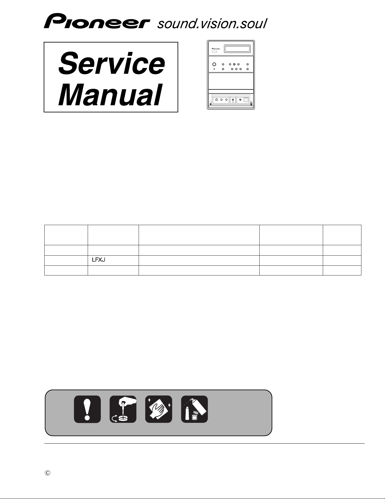
XV-HA5
DVD/CD RECEIVER
XV-HA5
THIS MANUAL IS APPLICABLE TO THE FOLLOWING MODEL(S) AND TYPE(S).
Model Type Power Requirement
XV-HA5 WLXJ AC220-240V 3
XV-HA5
XV-HA5 NTXJ AC220V 3
AC110V 3
Regional restriction
codes (Region No.)
Remarks
For details, refer to "Important Check Points for Good Servicing".
T-ZZR AUG. 2005 printed in Japan
Page 2
1234
SAFETY INFORMATION
A
This service manual is intended for qualified service technicians ; it is not meant for the casual doit-yourselfer. Qualified technicians have the necessary test equipment and tools, and have been
trained to properly and safely repair complex products such as those covered by this
manual.Improperly performed repairs can adversely affect the safety and reliability of the product
and may void the warranty. If you are not qualified to perform the repair of this product properly and
safely, you should not risk trying to do so and refer the repair to a qualified service technician.
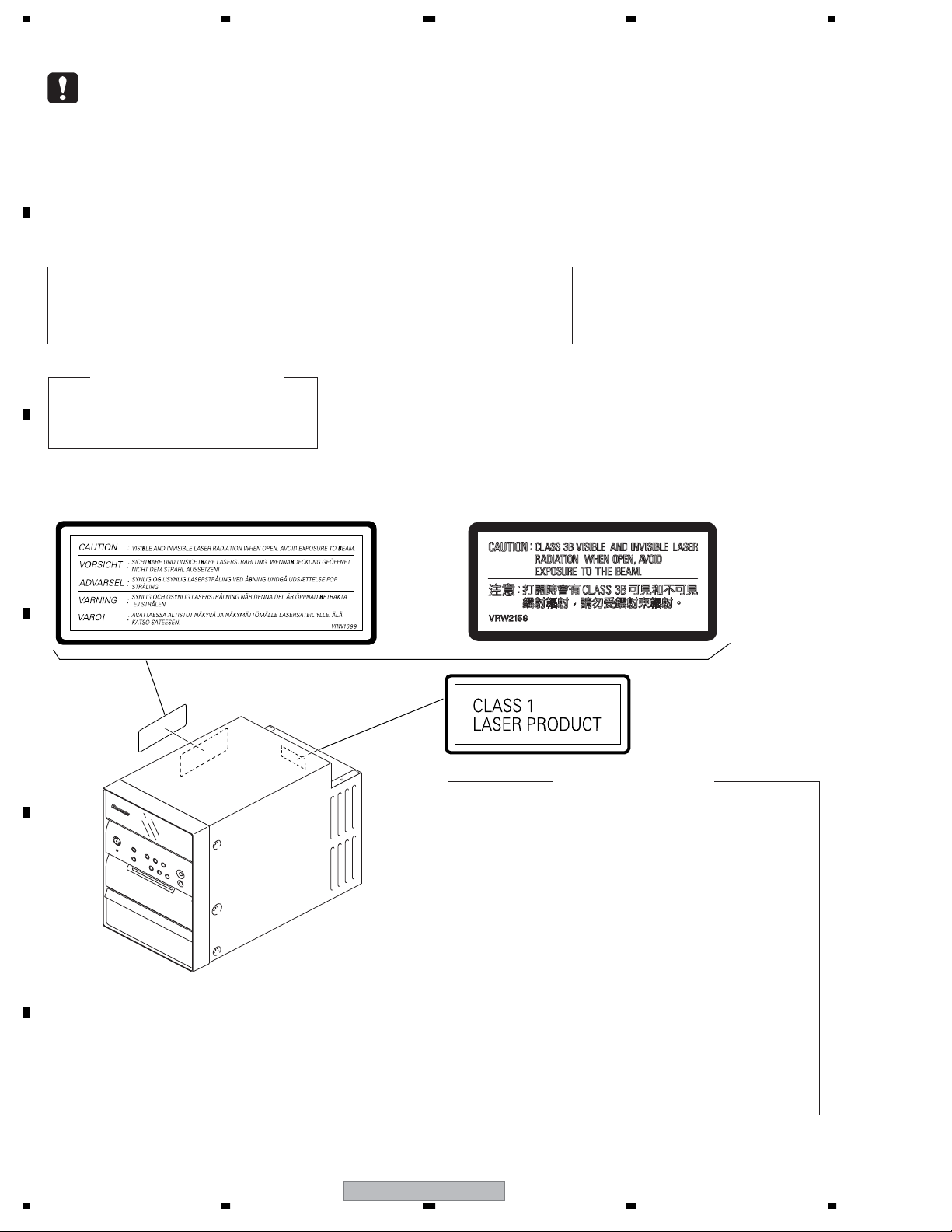
WARNING !
THE AEL (ACCESSIBLE EMISSION LEVEL) OF THE LASER POWER OUTPUT IS LESS THAN CLASS 1
BUT THE LASER COMPONENT IS CAPABLE OF EMITTING RADIATION EXCEEDING THE LIMIT FOR
B
CLASS 1.
A SPECIALLY INSTRUCTED PERSON SHOULD DO SERVICING OPERATION OF THE APPARATUS.
LASER DIODE CHARACTERISTICS
FOR DVD : MAXIMUM OUTPUT POWER : 5 mW
FOR CD : MAXIMUM OUTPUT POWER : 7 mW
WAVELENGTH : 650 nm
WAVELENGTH : 780 nm
LABEL CHECK
C
D
E
WLXJ, NTXJ types VRW1699
(Printed on the Rear Panel HAL)
LFXJ type VRW2159
Additional Laser Caution
1. Laser Interlock Mechanism
• Loading switch (S101 on the LOAB Assy) is used for interlock
mechanism of the laser.
When this switch turned ON in SW2 (CLOSE) side (OPEN signal is
0V and CLOSE signal is 3.5V), a laser becomes the status which can
completely oscillation.
Furthermore, the laser completely oscillates in the disc judgment and
disc playback.
When player is power ON state and laser diode is not completely
oscillating, 780nm laser diode is always oscillating by half power.
• Laser diode is driving with Q307 (650nm LD) and Q308 (780nm LD)
on the DVDM Assy.
Therefore, when short-circuit between the emitter and collector of these
transistors or the base voltage is supplied for transistors turn on, the
laser oscillates. (failure mode)
• In the test mode ∗ , there is the mode that the laser oscillates except
for the disc judgment and playback. LD ON mode in the test mode
oscillates with the laser forcibly.
The interlock mechanism mentioned above becomes invalid in this
mode.
2. When the cover is open, close viewing through the objective lens with
the naked eye will cause exposure to the laser beam.
F
2
1234
XV-HA5
∗ : Refer to page 63.
Page 3
5678
[Important Check Points for Good Servicing]
In this manual, procedures that must be performed during repairs are marked with the below symbol.
Please be sure to confirm and follow these procedures.
1. Product safety
Please conform to product regulations (such as safety and radiation regulations), and maintain a safe servicing environment by
following the safety instructions described in this manual.
1 Use specified parts for repair.
Use genuine parts. Be sure to use important parts for safety.
2 Do not perform modifications without proper instructions.
Please follow the specified safety methods when modification(addition/change of parts) is required due to interferences such as
radio/TV interference and foreign noise.
3 Make sure the soldering of repaired locations is properly performed.
When you solder while repairing, please be sure that there are no cold solder and other debris.
Soldering should be finished with the proper quantity. (Refer to the example)
4 Make sure the screws are tightly fastened.
Please be sure that all screws are fastened, and that there are no loose screws.
5 Make sure each connectors are correctly inserted.
Please be sure that all connectors are inserted, and that there are no imperfect insertion.
6 Make sure the wiring cables are set to their original state.
Please replace the wiring and cables to the original state after repairs.
In addition, be sure that there are no pinched wires, etc.
7 Make sure screws and soldering scraps do not remain inside the product.
Please check that neither solder debris nor screws remain inside the product.
8 There should be no semi-broken wires, scratches, melting, etc. on the coating of the power cord.
Damaged power cords may lead to fire accidents, so please be sure that there are no damages.
If you find a damaged power cord, please exchange it with a suitable one.
9 There should be no spark traces or similar marks on the power plug.
When spark traces or similar marks are found on the power supply plug, please check the connection and advise on secure
connections and suitable usage. Please exchange the power cord if necessary.
0 Safe environment should be secured during servicing.
When you perform repairs, please pay attention to static electricity, furniture, household articles, etc. in order to prevent injuries.
Please pay attention to your surroundings and repair safely.
A
B
C
D
2. Adjustments
To keep the original performance of the products, optimum adjustments and confirmation of characteristics within specification.
Adjustments should be performed in accordance with the procedures/instructions described in this manual.
3. Lubricants, Glues, and Replacement parts
Use grease and adhesives that are equal to the specified substance.
Make sure the proper amount is applied.
4. Cleaning
For parts that require cleaning, such as optical pickups, tape deck heads, lenses and mirrors used in projection monitors, proper
cleaning should be performed to restore their performances.
5. Shipping mode and Shipping screws
To protect products from damages or failures during transit, the shipping mode should be set or the shipping screws should be
installed before shipment. Please be sure to follow this method especially if it is specified in this manual.
56
XV-HA5
E
F
3
7
8
Page 4

1234
CONTENTS
SAFETY INFORMATION..................................................................................................................................... 2
1. SPECIFICATIONS ............................................................................................................................................ 5
2. EXPLODED VIEWS AND PARTS LIST ............................................................................................................ 6
A
B
C
D
E
2.1 PACKING ................................................................................................................................................... 6
2.2 EXTERIOR SECTION................................................................................................................................ 8
2.3 FRONT PANEL SECTION ....................................................................................................................... 10
2.4 05 LOADER ASSY................................................................................................................................... 12
2.5 Traverse Mechanism Assy-S.................................................................................................................... 14
3. BLOCK DIAGRAM AND SCHEMATIC DIAGRAM ..........................................................................................16
3.1 BLOCK DIAGRAM ................................................................................................................................... 16
3.2 OVERALL WIRING CONNECTION DIAGRAM........................................................................................ 18
3.3 DVDM ASSY (1/2).................................................................................................................................... 20
3.4 DVDM ASSY (2/2).................................................................................................................................... 22
3.5 IF ASSY (1/2)........................................................................................................................................... 24
3.6 IF (2/2) and DISP ASSYS ........................................................................................................................ 26
3.7 HP 2 ASSY .............................................................................................................................................. 28
3.8 REGULATOR and POWER ASSYS......................................................................................................... 30
3.9 SECONDARY and PRIMARY ASSYS ..................................................................................................... 32
3.10 KARAOKE ASSY ................................................................................................................................... 34
3.11 WAVEFORMS........................................................................................................................................ 36
4. PCB CONNECTION DIAGRAM ..................................................................................................................... 39
4.1 LOAB ASSY............................................................................................................................................. 39
4.2 DVDM ASSY............................................................................................................................................ 40
4.3 IF ASSY ................................................................................................................................................... 42
4.4 DISP ASSY .............................................................................................................................................. 46
4.5 HP2, REGULATOR and POWER ASSYS................................................................................................ 48
4.6 SECONDARY ASSY ................................................................................................................................ 50
4.7 PRIMARY ASSY ...................................................................................................................................... 52
5. PCB PARTS LIST ........................................................................................................................................... 56
6. ADJUSTMENT ............................................................................................................................................... 61
6.1 ADJUSTMENT ITEMS AND LOCATION ................................................................................................. 61
6.2 JIGS AND MEASURING INSTRUMENTS............................................................................................... 61
6.3 NECESSARY ADJUSTMENT POINTS ................................................................................................... 62
6.4 TEST MODE ............................................................................................................................................ 63
6.5 MECHANISM ADJUSTMENT.................................................................................................................. 64
7. GENERAL INFORMATION ............................................................................................................................. 66
7.1 DIAGNOSIS ............................................................................................................................................. 66
7.1.1 TEST MODE ...................................................................................................................................... 66
7.1.2 DISPLAY SPECIFICATION OF THE TEST MODE............................................................................ 67
7.1.3 FUNCTIONAL SPECIFICATION OF THE SHORTCUT KEY ............................................................ 68
7.1.4 SPECIFICATION OF MODEL INFORMATION DISPLAY.................................................................. 69
7.1.5 FUNCTIONAL SPECIFICATION OF THE SERVICE MODE............................................................. 70
7.1.6 SERVICE TEST MODE ..................................................................................................................... 71
7.1.7 METHOD FOR DIAGNOSING DEGRADATION OF THE LDs ON THE PICKUP ASSY................... 72
7.1.8 DVD TROUBLE SHOOTING.............................................................................................................. 73
7.1.9 ID NUMBER AND ID DATA SETTING ............................................................................................... 76
7.1.10 SEQUENCE AFTER POWER ON/0FF ........................................................................................... 79
7.1.11 SYSTEM COMPUTER PROTECT SPECIFICATION ...................................................................... 83
7.1.12 PROTECTION CIRCUIT.................................................................................................................. 86
7.1.13 DISASSEMBLY ................................................................................................................................ 88
7.2 PARTS.................................................................................................................................................... 100
7.2.1 IC ..................................................................................................................................................... 100
7.2.2 DISPLY ............................................................................................................................................ 105
8. PANEL FACILITIES ...................................................................................................................................... 106
F
4
1234
XV-HA5
Page 5
5678
1. SPECIFICATIONS
• Amplifier section
Front . . . . . . . . . . . . . . . . . . . 25 W per channel
(1 kHz, 10 % T.H.D., 4 Ω)
• Disc section
Digital audio
characteristics . . . . . . . . DVD fs: 96 kHz, 24-bit
Type . . . . . DVD system, Video CD/Super VCD
system and Compact Disc
digital audio system
Frequency
response . . . 4 Hz to 44 kHz (96kHz sampling) /
4 Hz to 22 kHz (48kHz sampling)
Wow and Flutter . . . . . . . Limit of measurement
(±0.001 % W.PEAK) or less (JEITA)
• FM tuner section
Frequency range . . . . . . 87.5 MHz to 108 MHz
Antenna . . . . . . . . . . . . . . . . 75 Ω, unbalanced
• AM tuner section
Frequency range
With 9kHz step . . . . . . 531 kHz to 1,602 kHz
With 10kHz step . . . . . 530 kHz to 1,700 kHz
Antenna . . . . . . . . . . . . . . . . . . . Loop antenna
• Miscellaneous
Power requirements:
Singapore / Malaysia/ Thailand
models . . . . . . . . . . AC 220-240 V, 50/60 Hz
Taiwan model . . . . . . . . . . . AC 110 V, 60 Hz
Power consumption:
Singapore / Malaysia / Thailand
models . . . . . . . . . . . . . . . . 79 W
Taiwan model . . . . . . . . . . . . . . . . . . . . 71 W
Power consumption in standby:
Singapore / Malaysia / Thailand
models . . . . . . . . . . . . . . 0.37 W
Taiwan model. . . . . . . . . . . . . . . . . . . 0.27 W
Dimensions . . 170(W) x 252(H) x 321.4(D) mm
Weight . . . . . . . . . . . . . . . . . . . . . . . . . . 5.3 kg
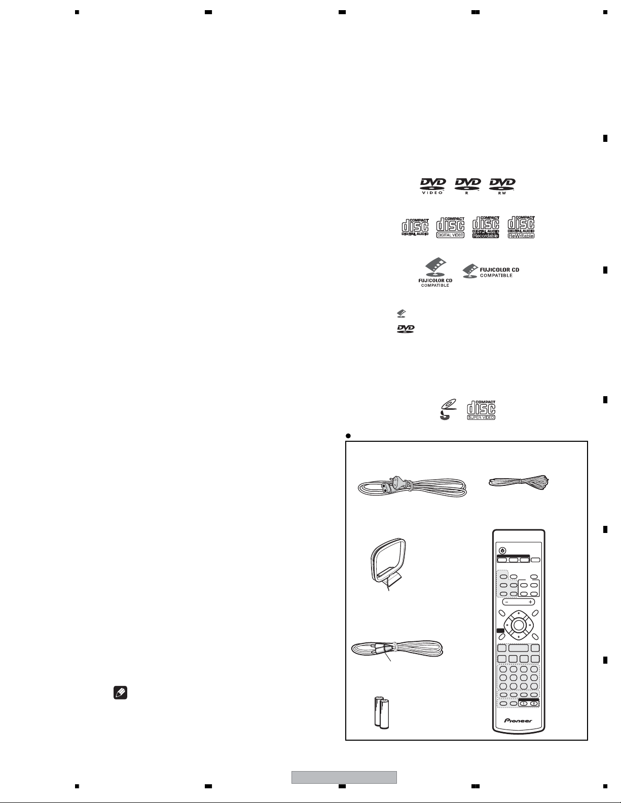
• Accessories (DVD/CD receiver)
Remote control . . . . . . . . . . . . . . . . . . . . . . . . 1
AA/R6 dry cell batteries . . . . . . . . . . . . . . . . . 2
Video cable (yellow plugs) . . . . . . . . . . . . . . . 1
AM loop antenna . . . . . . . . . . . . . . . . . . . . . . 1
FM antenna . . . . . . . . . . . . . . . . . . . . . . . . . . 1
Power cord . . . . . . . . . . . . . . . . . . . . . . . . . . . 1
These operating instructions . . . . . . . . . . . . . 1
Speaker system
Enclosure . . . . . . . Bass-reflex bookshelf type
System . . . . . . . . . . . . . . . 10 cm 2-way system
Speakers:
Woofer . . . . . . . . . . . . . . . . . . 10 cm cone type
Tweeter . . . . . . . . . . . . 2.6 cm semi-dome type
Nominal impedance . . . . . . . . . . . . . . . . . . 4 Ω
Frequency range . . . . . . . . . . . 50 Hz to 60 kHz
Maximum Input Power . . . . . . . . . . . . . . . 25 W
Dimensions . . . 140(W) x 250(H) x 253(D) mm
Weight . . . . . . . . . . . . . . . . . . . . . . . . . . 2.5 kg
(magnetically shielded)
• Accessories (speakers)
Non-skid pads . . . . . . . . . . . . . . . . . . . . . . . . 8
Note
•
Specifications and design subject to
possible modification without notice, due
to improvements.
Disc / content format playback
compatibility
This player is compatible with a wide range of
disc types (media) and formats. Playable discs
will generally feature one of the following logos
on the disc and/or disc packaging. Note
however that some disc types, such as
recordable CD and DVD, may be in an
unplayable format.
See the Disc compatibility table below for more
information.
DVD-Video DVD-R DVD-RW
Audio CD CD-R
• is a trademark of Fuji Photo Film Co. Ltd.
• is a trademark of DVD Format/Logo
Licensing Corporation
• Also compatible with KODAK Picture CD
This player supports the IEC’s Super VCD standard for superior picture quality, dual
soundtracks, and widescreen support.
Accessories
• Power cord
(WLXJ, NTXJ : ADG1154)
(LFXJ : ADG7097)
• AM Loop Antenna
(ATB7013)
• Video Cable
(L = 1.5m) (VDE1065)
Yellow
• Dry Cell Batteries
Video CD
Super Video CD (Super VCD)
Fujicolor CD
VIDEO
CD
CD-RW
• FM Antenna (ADH7030)
• Remote Control
(XXD3100)
STANDBY/ON
DVD/CD
FUNCTION
FM/AM
TIMER/
CLOCK ADJ.
SFC AUDIO
VOLUME
TUNE +
ENTER
TUNE -
2 3
ECHO
INPUT
ANGLE ZOOMMUTE SOUND
DEFABC
MNOGHI JKL
WXYZ MARKPQRS TUV
PROGRAM
KEY CONTROL
DVD
ST +ST -
SYSTEM
SETUP
SUBTITLE
RETURN
CLEAR
ENTER
DISP/CHARA
DVD/CD
BASS
BOOST
VIRTUAL
SURROUND
TOP MENU DVD MENU
HOME
MENU
1
4 5 6
7 8 9 0
REPEAT RANDOM
KARAOKE
A
B
C
D
E
F
56
XV-HA5
5
7
8
Page 6
1234
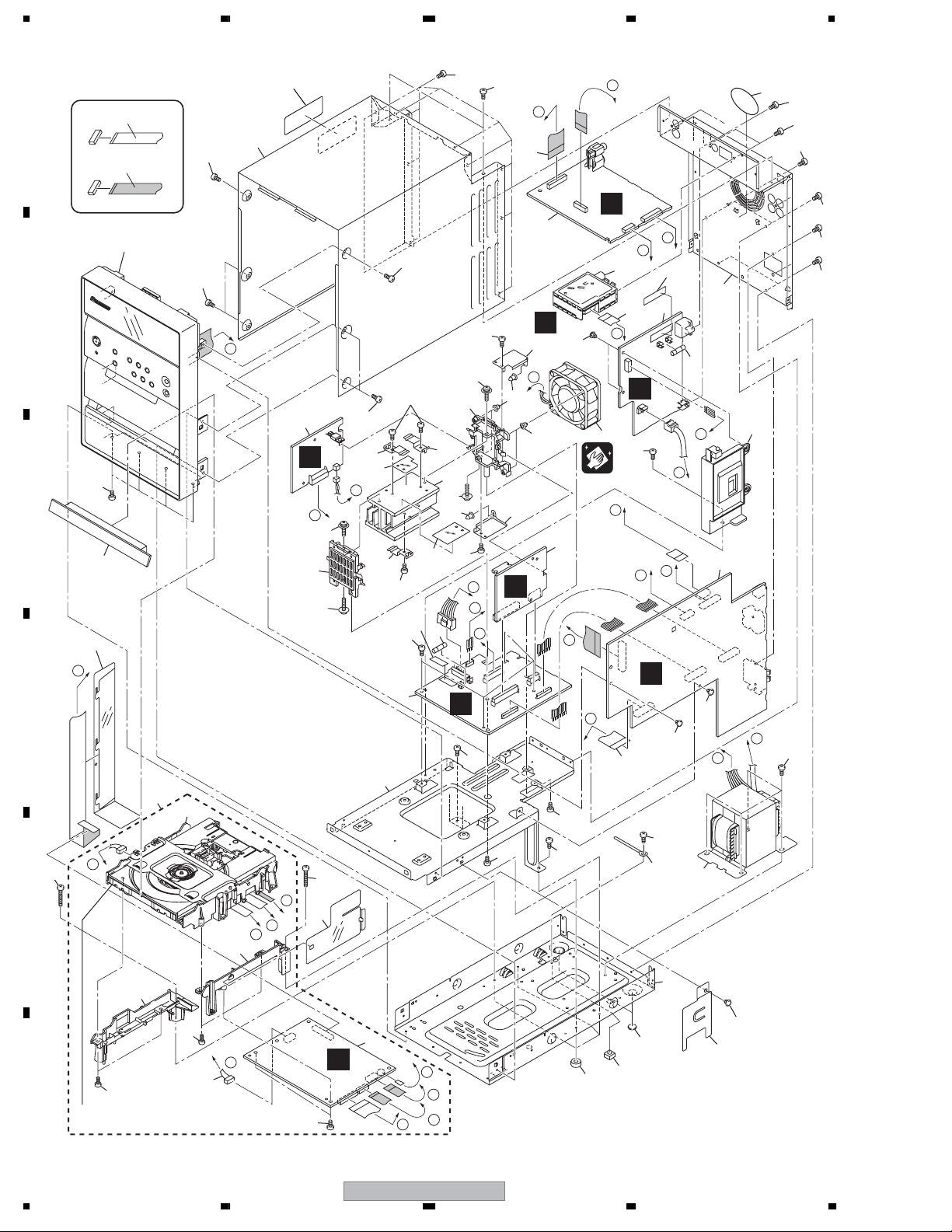
2. EXPLODED VIEWS AND PARTS LIST
NOTES:
A
Parts marked by "NSP" are generally unavailable because they are not in our Master Spare Parts List.
The mark found on some component parts indicates the importance of the safety factor of the part.
Therefore, when replacing, be sure to use parts of identical designation.
Screws adjacent to mark on product are used for disassembly.
For the applying amount of lubricants or glue, follow the instructions in this manual.
(In the case of no amount instructions, apply as you think it appropriate.)
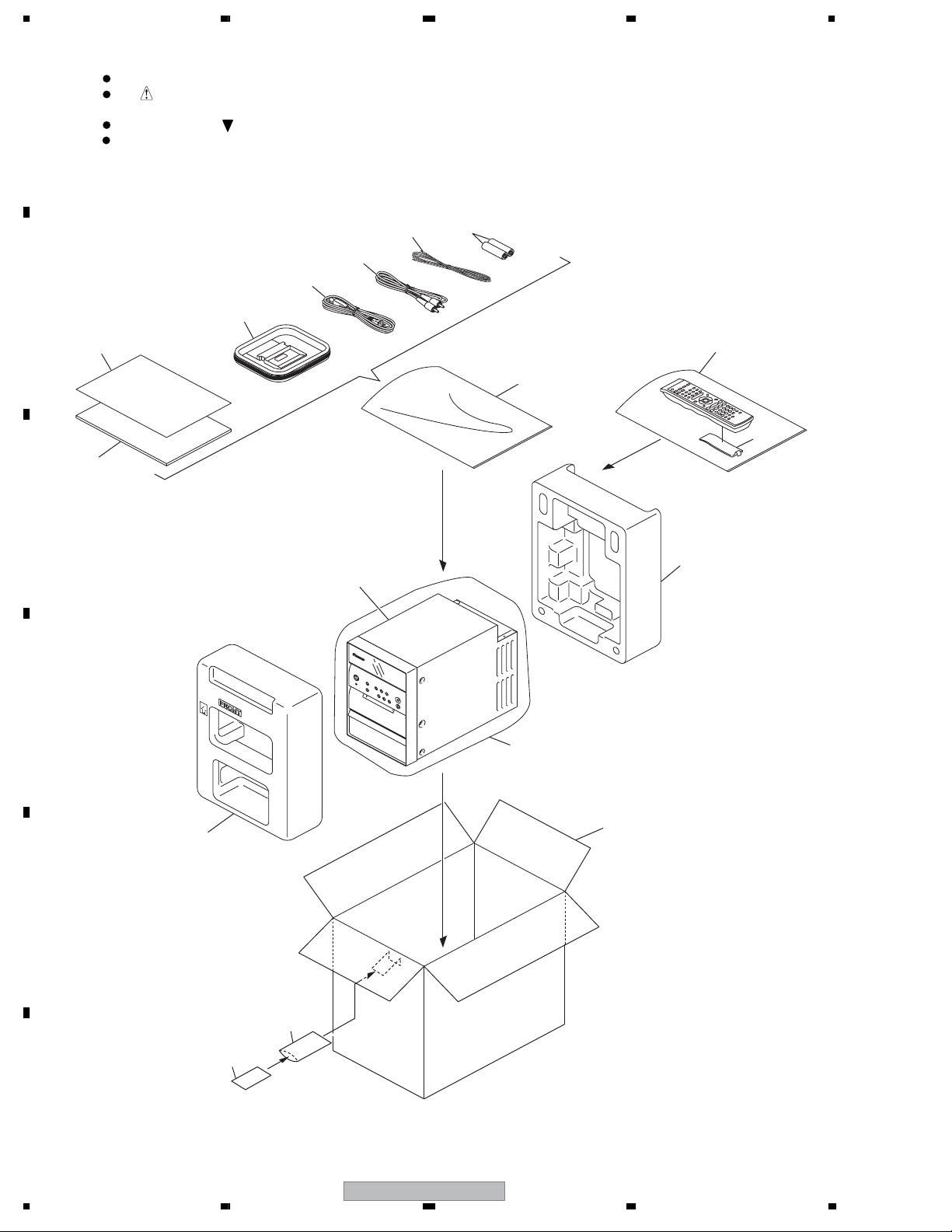
2.1 PACKING
B
16
1
C
8
6
7
5
4
2
11
3
14
XV-HA5
D
12
15
13
E
10
9
F
6
1234
XV-HA5
Page 7
5678
(1) PACKING SECTION PARTS LIST
No. Description Part No.
Mark
1 Operating Instructions See Contrast table(2)
2 Remote Control XXD3100
3 Battery Cover AZN7933
4 AM Loop Antenna ATB7013
5Power Cord See Contrast table(2)
6 FM Antenna ADH7030
7 Video Cable VDE1065
NSP 8 Dry Cell Batteries(R6P,AA) VEM1031
NSP 9 Warranty Card See Contrast table(2)
NSP 10 Vinyl Bag See Contrast table(2)
No. Description Part No.
Mark
NSP 11 Literature Bag AHG1180
12 Packing Sheet AHG7053
13 Front Pad XHA3154
14 Rear Pad XHA3155
15 Packing Case See Contrast table(2)
NSP 16 Service Map See Contrast table(2)
A
(2) CONTRAST TABLE
XV-HA5/WLXJ, LFXJ and XV-HA5/NTXJ are constructed the same except for the following:
Mark No. Description
1 Operating Instructions XRE3112 XRE3112 Not used
(English/Chinese)
1 Operating Instructions Not used Not used XRC3208
(Thai)
Power Cord
5
NSP 9 Warranty Card Not used Not used XRY3004
NSP 10 Vinyl Bag Not used Not used AHG7031
15 Packing Case XHD3551 XHD3551 XHD3553
NSP 16 Service Map Not used Not used XRY3005
XV-HA5
/WLXJ
ADG1154 ADG7097 ADG1154
>
>
XV-HA5
/LFXJ
XV-HA5
/NTXJ
B
C
D
56
XV-HA5
E
F
7
7
8
Page 8
1234
2.2 EXTERIOR SECTION
A
B
C
D
E
NON-CONTACT
SIDE
CONTACT SIDE
Refer to "2.3 FRONT PANEL SECTION"
52
45
42
C
18
M
59
19
52
57
23
36
10
26
27
50
33
51
58
39
50
51
C
15
4
33
25
G
25
H
M
35
33
6
A
58
K
J
G
17
47
57
A
5
52
F
H
G
50
38
50
51
26
37
26
51
51
To "2.3 FRONT PANEL
C
SECTION
K
E
8
13
F
I
12
51
Cleaning paper
GED-008
F
E
48
56
51
54
51
D
24
29
2
11
J
I
D
44
1
58
51
C
21
3
30
59
N
41
O
P
H
51
58
51
58
40
51
35
35
I
K
9
53
L
14
31
28
35
43
20
60
M
60
F
Refer to "2.4 05 LOADER ASSY"
22
60
8
1234
B
7
N
O
P
L
XV-HA5
32
34
Page 9
5678
(1) EXTERIOR SECTION PARTS LIST
No. Description Part No.
Mark
1 IF Assy See Contrast table (2)
2 PRIMARY Assy See Contrast table (2)
3 SECONDARY Assy XWZ4042
4 KARAOKE Assy XWZ4043
5 REGULATOR Assy XWZ4039
6POWER Assy XWZ4040
7DVDM Assy AWM7966
8 FM/AM TUNER Unit AXX7173
9Power Transformer XTS3098
10 FU2 Fuse (T5.0A/ 250V) REK1029
11 FU1 Fuse See Contrast table (2)
12 DC Fan Motor AXM7025
13 11P FFC/30V XDD3174
14 25P FFC/30V XDD3175
15 27P FFC/30V XDD3176
16 • • • • • •
17 CAUTION Label See Contrast table (2)
NSP 18 DVD ASSY XXA3036
NSP 19 05 Loader Assy VWT1219
20 Adaptor 05L XNW3014
21 Adaptor 05R XNW3015
22 Connector Assy PG05KK-E07
NSP 23 FUSE Card See Contrast table (2)
NSP 24 FUSE Card AAX7098
25 Insulation Plate AND7055
26 FET Bracket A ANG7432
27 Heat Sink ANH7169
NSP 28 Chassis HAL XNA3025
29 Rear Panel HAL See Contrast table (2)
30 Mecha Frame XNG3136
No. Description Part No.
Mark
31 Leg AEB7090
NSP 32 Spacer AEB7092
33 Insulation Rubber AEB7256
34 S Cover AEB7262
35 Push Rivet AEC7205
36 Mica Sheet A AEE7049
37 Mica Sheet B AEE7050
38 Rear Mold AMR7437
39 Fan Mold AMR7470
40 Cord Clamper RNH-184
41 DVD Barrier XEC3060
42 FFC Barrier XEC3061
43 FFC Cover XEC3067
44 PCB Suppor t XMR3096
45 Tray Cap XAK3491
46 • • • • • •
47 Bonnet Case XZN3177
NSP 48 SISIR Label See Contrast table (2)
49 • • • • • •
50 Screw 3*10 ABA7117
51 Screw BBZ30P060FTC
52 Screw BBZ30P080FNI
53 Screw BBZ40P060FTC
54 Screw BCZ30P060FTC
55 • • • • • •
>
>
>
56 Screw PPZ30P080FNI
57 Screw VPZ30P080FNI
58 Screw VPZ30P080FTC
59 Screw XBA3015
60 Screw BPZ30P080FNI
A
B
C
D
(2) CONTRAST TABLE
XV-HA5/WLXJ, LFXJ and XV-HA5/NTXJ are constructed the same except for the following:
Mark No. Description
1 IF Assy XWZ4033 XWZ4049 XWZ4050
2 PRIMARY Assy XWZ4041 XWZ4044 XWZ4041
>
NSP 23 FUSE Card AAX2367 AAX2377 AAX2367
NSP 48 SISIR Label XAX3525 Not used Not used
11 FU1 Fuse REK1021 REK1024 REK1021
17 CAUTION Label VRW1699 VRW2159 VRW1699
29 Rear Panel HAL XNC3342 XNC3388 XNC3389
XV-HA5
/WLXJ
(T800mA/ 250V) (T1.6A/ 250V) (T800mA/ 250V)
XV-HA5
56
XV-HA5
/LFXJ
XV-HA5
/NTXJ
7
E
F
9
8
Page 10
1234
2.3 FRONT PANEL SECTION
A
NON-CONTACT
SIDE
CONTACT SIDE
B
24
1
D
To "2.2 EXTERIOR
SECTION
A
4
22
14
C
8
5
D
11
15
26
16
20
24
21
23
17
25
3
12
6
B
C
To "2.2 EXTERIOR
SECTION
24
2
E
9
10
B
E
19
18
F
10
1234
XV-HA5
7
13
Page 11

5678
(1) FRONT PANEL SECTION PARTS LIST
No. Description Part No.
Mark
1 DISPLAY Assy XWZ4034
2 HP2 Assy XWZ4035
3 13P FFC/30V XDD3171
4 29P FFC/30V XDD3173
5 Door Spring XNG3138
6 Gnd Plate B XNG3140
7 Leg AEB7090
8 Pioneer Name Plate AAM7012
9 Func Button A XAD3219
10 Func Button B XAD3222
11 Tray Cap XAK3491
12 Standby Button Assy XXG3212
13 Front Panel Assy XXG3215
14 Display Window XAK3489
15 Sealing Panel XAK3495
16 Door Cover XAK3517
17 Timer Lens XAK3500
18 Door XAN3055
19 Sub Cushion XEB3048
20 Door Cushion XEB3049
A
B
C
21 Front Panel XMB3202
NSP 22 Standby Button XAD3221
NSP 23 Standby Lens XAK3490
24 Screw VPZ30P080FTC
25 DM Screw DBA1260
26 MIC Knob XAA3031
D
E
56
XV-HA5
F
11
7
8
Page 12
1234
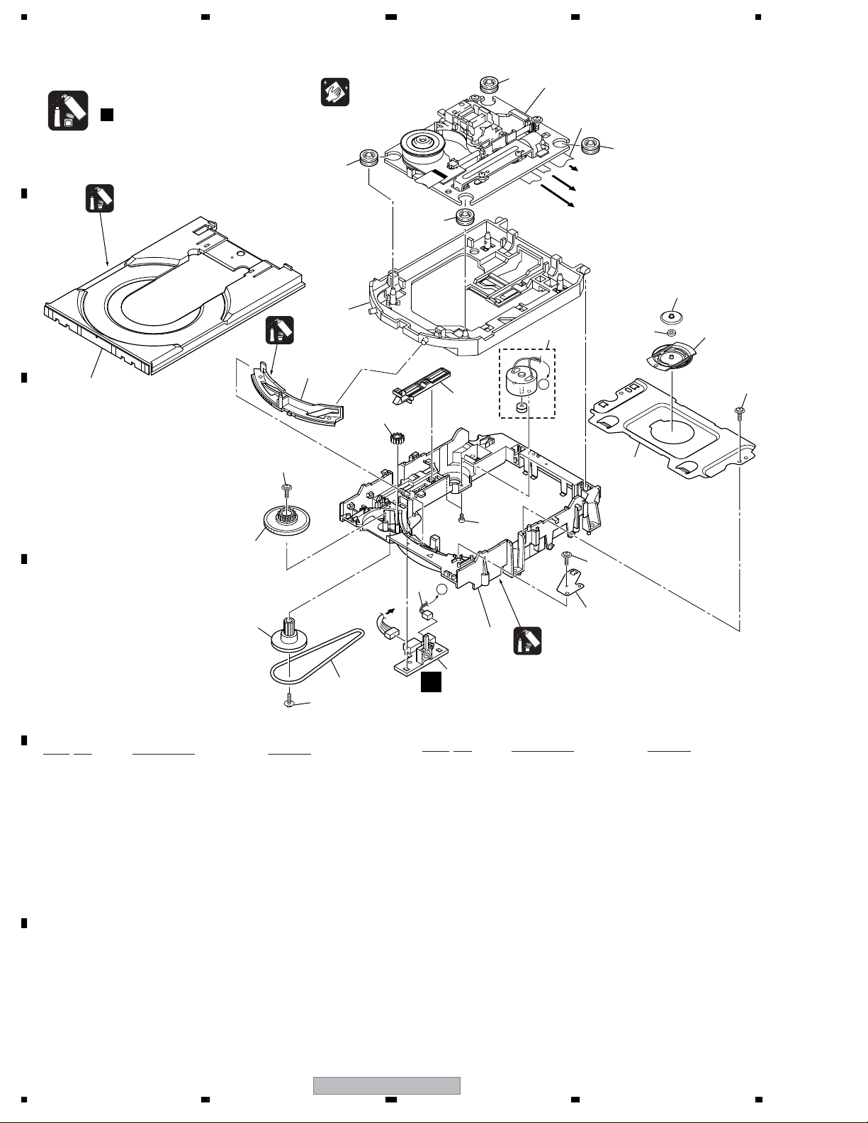
2.4 05 LOADER ASSY
A
B
C
Note :
Refer to
" Application of Lubricant".
Daifree
GEM1036
23
Lubricating Oil
GYA1001
13
22
Pickup leneses
Cleaning liquid
GEM1004
Cleaning paper
GED-008
8
12
16
8
2
Refer to
"2.5 Traverse Mechanism Assy-S".
6
8
To DVDM CN101 (Pickup)
To DVDM CN104 (Stepping Motor)
To DVDM CN102 (Spindle Motor)
8
18
17
3
A
24
19
20
22
15
14
D
05 LOADER ASSY PARTS LIST
Mark
No. Description Part No.
NSP 1 LOAB Assy VWG2346
2Traverse Mechanism Assy-S DXX2568
3 Loading Motor Assy VXX2912
E
4• • • • •
5• • • • •
6 Flexible Cable (24P) VDA2008
7 Connector Assy 2P VKP2253
8 Floating Rubber VEB1351
9 Belt VEB1358
10 Stabilizer VNE2253
22
To
DVDM CN103
9
21
22
7
A
11
1
A
Mark
No. Description Part No.
16 Drive Gear VNL1923
17 SW Lever VNL1925
18 Clamper Plate 04 VNE2342
19 Bridge 04 VNE2343
20 Clamper 04 VNL1969
21 Screw JGZ17P028FTC
22 Screw VBA1094
23 Tray VNL1920
24 Clamp Magnet VMG1029
10
Lubricating Oil
GYA1001
11 Loading Base VNL1917
12 Float Base 04 VNL1968
F
13 Drive Cam VNL1919
14 Gear Pulley VNL1921
15 Loading Gear VNL1922
12
1234
XV-HA5
Page 13
5678
Application of Lubricant
Lubricating Oil
GYA1001
No. 11
Loading Base
No. 13
Drive Cam
Lubricating Oil
GYA1001
Around the shaft
Lubricating Oil
GYA1001
Lubricating Oil
GYA1001
Inner side of a ditch
A
B
Lubricating Oil
GYA1001
Inner side of a ditch
C
Lubricating Oil
GYA1001
Lubricating Oil
GYA1001
Front View Rear View
No. 23
Tray
Daifree
GEM1036
Concave of unevenness
No. 23
Tray
Top View Bottom View
Concave of unevenness
Daifree
GEM1036
Inner side of a ditch
Daifree
GEM1036
No. 13
Drive Cam
D
Daifree
GEM1036
Concave of unevenness
E
Side of the rib
Daifree
GEM1036
F
56
XV-HA5
13
7
8
Page 14
1234
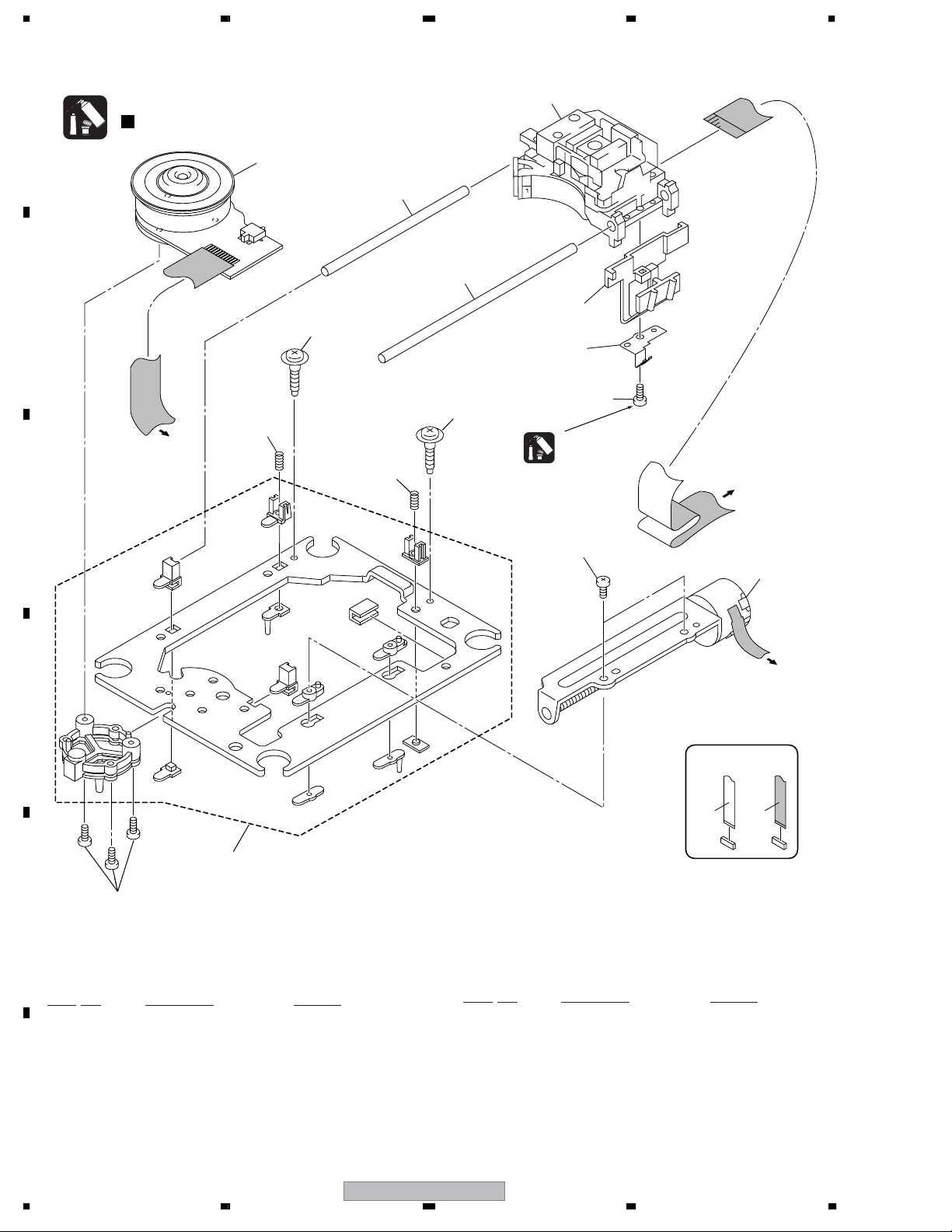
2.5 Traverse Mechanism Assy-S
Note :
A
B
C
Refer to
" Application of Lubricant".
Note : When part #2 is replaced,
2
11
To DVDM CN102
(Spindle Motor)
part #13 also need to be
replaced at the same time.
4
3
10
10
11
1
5
6
9
Silicone Adhesive
GEM1037
To
DVDM CN101
(Pickup Assy)
D
8
Note : Spindle screw (DBA1252) of No.13 is the screw which applied special bond.
E
13
Therefore the adhesion becomes ineffective when takes it off once. Spindle screw is the part which cannot recycle.
When part #2 is replaced, part #13 also need to be replaced at the same time.
Traverse Mechanism Assy-S PARTS LIST
No. Description Part No.
Mark
1 05SD Pickup Assy-S OXX8014
2 Spindle Motor N200 DXM1197
3 Guide Shaft VK1 DLA1940
4 Sub Guide Shaft VK1 DLA1941
NSP 5 Joint VK1B DNK4272
F
6 Joint Spring VK1 DBK1235
7 Stepping Motor VK1 DXM1201
12
>
NON-CONTACT
SIDE
Mark No. Description Part No.
NSP 8 Mechanism Frame VK1 DNK4160
9 Precision Screw VK1 DBA1209
10 Skew Screw VK1 DBA1211
11 Skew Spring VK1 DBH1516
NSP 12 Stepping Screw DBA1205
13 Spindle Screw VK1(for Service) DBA1252
7
To
DVDM CN104
(Stepping Motor)
CONTACT SIDE
14
XV-HA5
1234
Page 15

5678
A
B
C
D
E
56
XV-HA5
F
15
7
8
Page 16
1234
+ -
+ -
SC
Sy
FL
POWER SUPPLY
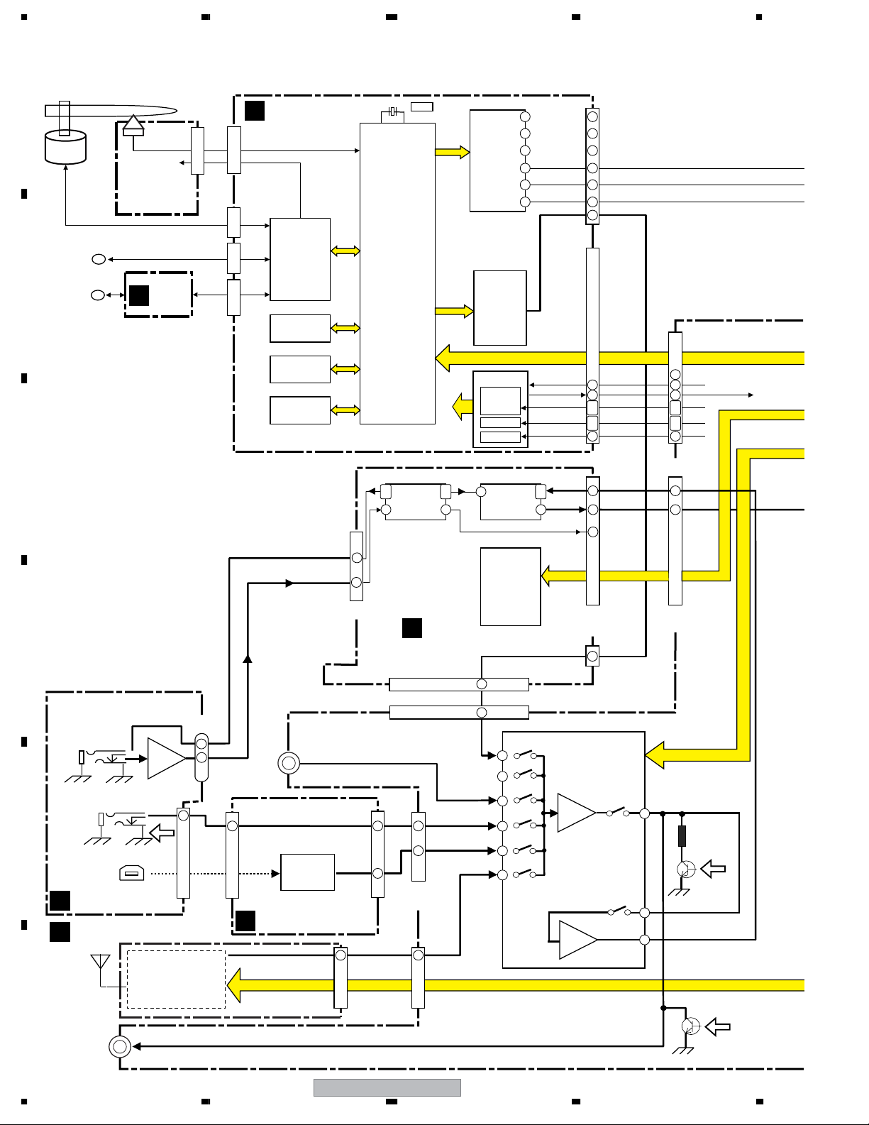
3. BLOCK DIAGRAM AND SCHEMATIC DIAGRAM
3.1 BLOCK DIAGRAM
A
SPINDLE
Motor
05SD PU
FOCS/TRKG
PlCK UP
ASSY
Stepping
M
Motor
+ -
B
Loading
Motor
+ -
M
A
LOAD
ASSY
CN1013
(24P)
CN103
(4P)
CN104
(5P)
DVDM ASSY
B
CN101
(24P)
CN102
(12P)
FTS&SPDL
DRlVER
IC101
BD7995EFS
IC204
16K
EEPROM
IC202
64M SDRAM
IC203
16M
FLASH ROM
MT1389FE/C2-L
·System Control
·RF Amp
·Servo Control
·AV Decoder
·108MHz 12bit Video
DAC
C
27MHz
BACK END IC
IC201
MIC
8
ECHO
IC8401
9
Bu9255FS
VlDEO AMP
8
2
DRlVER
IC401
MM1623BF
2CH DAC
IC501
PCM1753
POWER SUPPLY
1.8V:IC711
3.3V:IC731
5V:IC751
6.5V:IC761
12V:Q701
VOCAL
2
FADER
IC8301
BA3838F
16
20
18
23
26
21
CN902
(27P)
DVDPOWER
VDET
VPR+8
VPR+8M
VDVD+12
6
3
16
12
14
10
25
13
23
24
21
22
25
11
8
6
4
1
16
FL
CN901
(25P)
V
SC
Sy
CN5952
(25P)
DOUT
16
13
4
23
24
21
22
25
CN3101
(21P)
11
1
VDET
FL IN
L OUT
3
DVD
LINE IN
TUNER
KEY
CON
IC8201
M65847AFP
7
7
1
3
7
9
11
5
CN8301
(1/2)
(21P)
25
CN8502
(27P)
AUDIO INPUT SELECT
BD3841FS
IC3001
BUFFER
CN3101
(1/2)
(21P)
ATTENUATOR
RECA
26
IN1
18
20
OUT
-6dB
-6 dB ATT
(u-p)
REC MUTE
(u-p)
2
CN5105
(4P)
K
1/2
D
CN8301(2/2)
(21P)
CN3101(2/2)
J9911
MIC
AMP
(u-p)
AXA7173
(4P)
1
3
CN5421
(1/2)
(15P)
3
2
3
CN5921
D
LINE IN
(15P)
2/2
USB
RECEIVER
IC5201
PCM 2900EG
DISP ASSY
MIC SW
MIC IN
FRONT IN
E
USB IN
HP2 ASSY
2/2
E
M
TUNER MODULE
TUNER
2
IC9402
HA17558AF
FRONT IN DETECT
TUNER MODULE
(21P)
CN5911
(2/2)(2/2)
(29P)
6
F
KARAOKE ASSY
27
27
17
17
CN5951
(2/2)
(29P)
6
CN5701
(11P)
FRONT AUDIO IN
USB AUDIO
16
LINE OUT
XV-HA5
1234
Page 17
5678
16
12
14
8
6
10
CN8502
(27P)
KEY
14.15
14.15
MICROPROCESSOR
K
PDC 125
IC5501
KARAOKE ASSY
2/2
IR SENSOR
13
13
COMPOSITE
VIDEO OUT
S-VIDEO
OUT
CN5951(2/2)
(29P)
CN5911(2/2)
(29P)
IC3911
NJM4565M
3
HP. AMP
CN5911(1/2)
1
22
CN5951(1/2)
(29P)
(29P)
A
D
DISPLAY ASSY
1/2
B
LCD
With COG DRIVER
Positive: XAV3029-
1/2
E
(2/2)
(15P)
HP DETECT
(u-p)
HP2 ASSY
HEADPHONE
OUT
C
CN5921
(1/2)
(15P)
22
CN5421
8
8
ON/OFF
(u-p)
3
BASS
BOOST
IC3271
HA17558AF
1
SYSTEM MUTE
(u-p)
XPROTECT
(u-p)
9
CN42(1/2)
(11P)
J21(1/2)
(11P)
9
R3033,
R3034
15
E-VOLUME
IC3201
BD3814FV
-VOLUME
-ST-WIDE
-TONE
-SFC
27
H
C
IF ASSY
56
XV-HA5
AMP SECTION
POWER
G
ASSY
IC3301
1
13
2ch
Power Amp
LOW POWER AMP
TDA8560Q
MODULE
1
CN23
(15P)
CN3302
(15P)
SECONDARY ASSY
ANALOG AUDIO & VIDEO SIGNAL
DIGITAL AUDIO SIGNAL
CONTROL SIGNAL
OTHER
7
7
9
CN3301
(5P)
CN42
4
5
J21(2/2)
(2/2)
(11P)
21212
(11P)
CN24
(5P)
4
5
• R ch is same as L ch.
CN3352
(4P)
1
8
D
L/R OUT
E
F
17
Page 18
1234
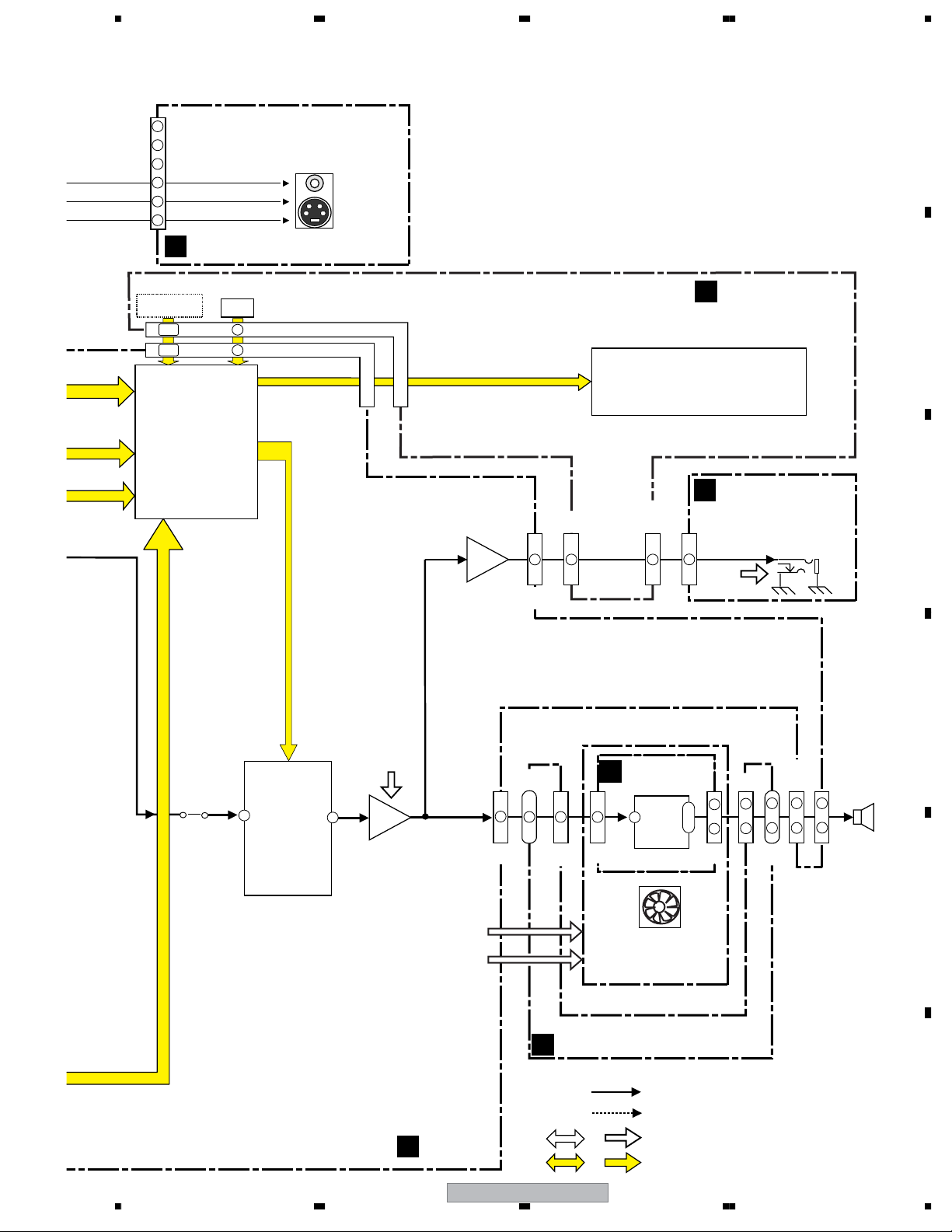
3.2 OVERALL WIRING CONNECTION DIAGRAM
A
JA9903
XKN3016
HP2 ASSY
JA9902
AKN7005
JA9901
AKN7005
JA9401
MIC
(MAIN)
AKN7005
JA9402
MIC
(SUB)
B
AKN7005
E
(XWZ4035)
2mm PITCH WIRE
GNDA
MIC SW
2143
MIC
VA+12
51048-0400
D20PYY0435E
J9911
CN9421
52045-1345
FA(R)
1
GNDA
FA(L)
3
GNDA
FADET
5
HPR
GNDHP
7
HPL
HPDET
9
GNDC
D-
11
D+
VBUS
13
CN5921
52044-1345
2
4
6
8
10
12
2
4
6
8
10
12
FFC (1.25mm PITCH)
XDD3171
FA(R)
1
GNDA
3
FA(L)
GNDA
FADET
5
HPR
GNDHP
7
HPL
HPDET
9
GNDC
D-
11
D+
VBUS
13
CN5911
DIMMER
GLED
1
52044-2945
2
2
1
GLED
HLEM295-1
DIMMER
CN5951
C 1/2,CC 2/2,
C
CN8301
XKP3081-
1
LOUT
2
GNDA
3
ROUT
4
GNDA
5
DVDR
6
GNDA
7
JA8502
AKB7146
D
VIDEO OUTPUT
(COMPOSITE+S OUT)
CN5105
52147-0410
VA+12
1
MIC
2
MIC SW
3
4
GNDA
K
KARAOKE ASSY
(XWZ4043)
DVDL
GNDA
FRIN
GNDA
FLIN
VA+12
KEYCONSTB
KEYCONCLK
KEYCONDATA
ECHOVOL
VOCAL A
VOCAL B
VOCAL C
GNDU
GNDU
8
9
10
11
12
13
14
15
16
17
18
19
20
21
CN3101
XKP3070-
LOUT
1
GNDA
2
ROUT
3
GNDA
4
DVDR
5
GNDA
6
7
DVDL
8
GNDA
FRIN
9
GNDA
10
FLIN
11
VA+12
12
13
KEYCONSTB
14
KEYCONCLK
BOARD TO BOARD (1.25mm PITCH)
15
KEYCONDATA
16
ECHOVOL
17
VOCAL A
18
VOCAL B
19
VOCAL C
GNDU
20
GNDU
21
IF ASSY
(XWZ4033:XV-HA5/WL)
(XWZ4049:XV-HA5/LF)
(XWZ4050:XV-HA5/NT)
P/XI
SQUEEZE
VSEL1SCASPECT
VSEL2
GNDDVGNDDSYGNDD
CY/G
Cb/B
GNDD
Cr/R
GNDDBG
GNDD
GNDD
GNDA
GNDDRGNDDFRGNDA
FL
573
1
VKN1258-
2
CN8502
E
LOADING
MOTOR
ASSY
: VXX2912
F
2
1
P/XI
VKN1258-
SQUEEZE
CN902
LOAD-
S5B-PH-SM3
CN104
1
CN602
LOAD-
2
1
3
VSEL2
LOAD+
A
9
13
4
11
6
10
17
15
16
1481820222624
12
XDD3176 FFC (1mm PITCH)
8
4
567
SC
VSEL1
ASPECT
SW2
LOAD+
342
21345
SW2
V+3D
LOAB ASSY
(VWG2346)
GNDD
V+3D
9
V
GNDDSYGNDD
SW1
5
SW1
CN601
12
10
CY/G
CN103
S5B-PH-K-S
14
131911
Cb/B
GNDD
AKN7035
171615
Cr/R
GNDD
ST1-
ST1+
2
2
STEPPING
GNDD
19
18
20
B
G
GNDD
B
ST2-
ST2+
413
413
MOTOR
232125
27
22
26
24
27
25
23
21
R
FL
FR
GNDA
GNDA
GNDD
GNDD
DVDM ASSY
(AWM7966)
H2+
H1-
H1+
A2A3A1
9
7
11
8
12
10
CN105
8
12
10
9
711351
A1A2A3
H1-
H2+
H1+
SPINDLE
H2-
H3+
H3-
6
RKN1053
4
6
H3-
H2-
H3+
MOTOR
GNDS
345
GNDS
V+5S
2
2
V+5S
INSIDE
1
INSIDE
A
18
XV-HA5
NCNCNCNC
VKN1256-
1
2
XDD3175
2104
VKN1256-
CN901 CN5952
FOCS RTN
CN101
241720
FOCS RTN
CN1013
VDET
345
3
NCNCNC
VDET
TRKG RTN
FOCS DRV
222324
TRKG RTN
FOCS DRV
GNDD
GNDD
6
6
5
GNDD
GNDD
TRKG DRV
VSHF
21
20
212223
VSHF
TRKG DRV
MDATA2
SDATA2
SCLK2
ACK
7
DVDPOWER
XDVDRST
XREADY
GNDD
9
8
10
121116
FFC (1mm PITCH)
8
12
719
11
ACK
GND
19
GND
MDATA2
LD(650)
18
18
LD(650)
GNDD
SCLK2
SDATA2
XREADY
XDVDRST
DVDPOWER
PD
LD(780)
GND
MDB2B1ACB4B3
MPD(780)
MPD(650)
171619
ADD7418
24P FFC
16
1312151411
PD
MD
GND
LD(780)
MPD(650)
MPD(780)
PICKUP ASSY
GNDD
DOUT
GNDD
GNDD
1718151413
181422
16
17
151319
DOUT
GNDD
GNDD
GNDD
VREF(2.1V)
11
896
1013121514
VKN1482
89456
10
A
B1
B2
VREF(2.1V)
GNDM
GNDM
OEICG
745
7
OEICG
GNDM
20
GNDM
C
VPR+8M
VPR+8M
21
221920
21
VPR+8M
VPR+8M
780/650
B4
780/650
VPR+8
VPR+8
VDVD+12
23
25
24
FFC (1.25mm PITCH)
24
23
25
VPR+8
VPR+8
VDVD+12
VCC
GND
3
1
2
2
1
3
B3
VCC
GND
DVD MODULE
GND
VSM
RDS
TXR
+9V
TXLDOGND
7
9
11
856
10
XDD3174
8
6104
9
+9V
TXL
TXR
RDS
VSM
GND
M
(AXX7173)
TUNER MODULE
XXA3036
GND
CN5701
CLKDICE
52045-1145
3
1
2
4
2
5117
1
3
DI
CE
DO
CLK
52045-1145
1234
Page 19
5678
V5901
posi:XAV3029- nega:XAV3030-
LCD
WITH COG DRIVER
51048-0900
DISP ASSY
D
(XWZ4034)
XLCDRST
VP+12
TMRLED
LCDCS
LCDCLK
VE+5
LCDDATA
GNDU
GNDD
REMOCON
VESW+5
7109
345
8
6
XDD3173 FFC (1.25mm PITCH)
8
4
6
10
7
5
VP+12
LCDCS
LCDCLK
XLCDRST
CN51
SYS U-COM DOWNLOAD
9
VE+5
LCDDATA
WEN/DI
HLEM7S-1
1
VESW+5
WD0
2
3
TMRLED
121116
12
11
GNDD
GNDU
REMOCON
WCLK
RST
VCC
3
5
4
XSUSPEND
KEY2
KEY1
16
151319
KEY2
KEY1
XSUSPEND
VSS
NC
7
6
VDDNCVSS
VREF
RESET
STB
SCK
DATA
NC
215437869
GNDA
USBL
USBR
1718151413
181422
17
USBL
USBR
GNDA
HPDET
20
HPDET
GNDA
21
21
GNDA
HPL
221920
HPL
GNDHP
23
23
GNDHP
CABLE HOLDER
(FOR LCD
INSERTION)
FADET
GNDA
HPR
FA(L)
25
27
24
262928
242628
252927
HPR
FA(L)
GNDA
FADET
JA4601
TOTX177PL
JA3001
VKB1047
CN3352
CN43
52147-1210
SYSPOW
CN42
52147-1110
XPROTECT
FA(R)
GNDA
FA(R)
GNDA
AKE7086-
GNDU
GNDM
GNDM
GNDD
GNDD
AC
UN+56
GLED
VA-12
VP+8
VP+8
RIN
GNDA
MUTE
VP+15
GNDP
L+-+
L-
R-
LIN
R+
R-
L-
L+
÷
When ordering service parts, be sure to refer to "EXPLODED VIEWS and PARTS LIST" or
"PCB PARTS LIST".
÷
The > mark found on some component parts indicates the importance of the safety factor
of the part. Therefore, when replacing, be sure to use parts of identical designation.
÷
-
+R+
12
11
10
9
8
7
6
5
4
3
2
1
11
10
9
8
7
6
5
4
3
2
1
: The power supply is shown with the marked box.
OPTICAL OUTPUT
L
LINE IN
R
L
LINEOUT
R
SPEAKER
J22
51048-1200
D20PYY1225E
12
GNDU
11
GNDM
10
GNDM
9
GNDD
8
GNDD
7
SYSPOW
6
AC
5
UN+56
4
GLED
3
VA-12
2mm PITCH WIRE
VP+8
2
1
VP+8
J21
51048-1100
D20PYY1125E
11
RIN
10
GNDA
9
LIN
8
XPROTECT
7
MUTE
6
VP+15
5
R+
R-
4
2mm PITCH WIRE
3
GNDP
2
L-
1
L+
CN24
2.5mm pitch
KM250NA5L
CN3301
HELP
52147-0510
CN26
2.0mm PITCH WIRE
1212543
J11
HELP
D20PYY0520E
51048-0500
KP250NA5
R+L-GNDPR-L+
13425
CN23
BtoB
12345
L-
R-
GNDP
L+
R+
SYSPOW
AC
GNDU
354
AC
SYSPOW
GNDA
LIN
KP250NA15
LIN
GNDA
KM250NA15L
CN3302
AN1
XKP3084
CN3
B5P9-VH
115
XTS3098
UN+56
* T2
12 5643
UN+56
SUB2
GNDU
SECONDARY ASSY
H
(XWZ4042)
STBY
GNDA
RIN
MUTE
321 45678910
2.5mm pitch
321 4567891011 12 1513 14
RIN
STBY
MUTE
GNDA
POWER ASSY
G
(XWZ4040)
AC POWER CORD
AC INLET
2
1
5
412
3
0
0
115
SUB2
SUB1
SUB2
SUB1
SUB2
SUB1
REF5V
(VP+15V)
SENSE
VP+15V
BtoB
REF5V
SENSE
VP+15V
(VP+15V)
I
PRIMARY ASSY
(XWZ4041: WL, NT)
(XWZ4044: LF)
MAIN
MAIN
SUB1
MAIN
MAIN
B6P-VH
CN21
GNDP
H/LCONT
GNDVP+15+B+B
GNDP
11 12 1513 14
GNDP
GNDP
H/LCONT
GNDVP+15
LOW POWER AMP ASSY
+B
CN22
+B
CN3303
UVP+8
VP+8
KP250NA10
BtoB
VP+8
UVP+8
KM250NA10L
F
2
1
CN3651
KM200SA2L
SENSE
VP+15
GNDVP+8
H/LCONT
2.5mm pitch
VP+15
GNDVP+8
REF5V
REF5V
H/LCONT
(VP+8)
321 45678910
321 45678910
(VP+8)
SENSE
REGULATOR ASSY
(XWZ4039)
XPROTECT
FANGND
FANGND
XPROTECT
A
B
C
D
E
+B(FAN)
+B(FAN)
F
56
XV-HA5
19
7
8
Page 20
1234
3.3 DVDM ASSY (1/2)
A
(RF)
B
LD Driver for CD
(RF)
(T)
(T)
(F)
(F)
LD Driver for DVD
C
FTS DRIVER
3
2
(F)
(T)
D
E
F
20
MOTOR
STEPPING
CN601 PICKUP ASSY CN1013SPINDLE MOTOR
A
B
1/2
A
1234
(S)
(S)
(S)
(S)
(RF)
: RF SIGNAL ROUTE
(D)
: AUDIO SIGNAL ROUTE(DIGITAL)
(F)
: FOCUS SERVO LOOP LINE
(T)
: TRACKING SERVO LOOP LINE
(S)
: STEPPING SERVO LOOP LINE
(C/V)
: VIDEO SIGNAL ROUTE
(R/Cr)
: VIDEO SIGNAL ROUTE(R/Cr)
(G/Y)
: VIDEO SIGNAL ROUTE(G/Y)
(B/Cb)
: VIDEO SIGNAL ROUTE(B/Cb)
(S_Y)
: S VIDEO SIGNAL ROUTE
(S_C)
: S VIDEO SIGNAL ROUTE
1
(F)
(F)
(F)
(T)
(T)
(S)
(S)
(S)
(S)
XV-HA5
(T)
AYW7069
Page 21
5678
(D)
!
(R/CY)
(B/Cb)
B
DVDM ASSY
1/2
A
(AWM7966)
(S_Y)
(S_C)
(G/Y)
(C/V)
B
C
MT1389FE/C2-L
D
E
56
XV-HA5
F
B
1/2
21
7
8
Page 22
1234
3.4 DVDM ASSY (2/2)
B
A
B
C
DVDM ASSY
2/2
(AWM7966)
(D)
D
E
F
B
2/2
A
22
1234
XV-HA5
Page 23
5678
A
1.8V Regulator
5.0V
3.3V Regulator
5V Regulator
7.8V
6.4V
Video Driver Amp
6.5V Regulator
(D)
CN5952
B
C 2/2
7.8V
C
NC
(D)
: AUDIO SIGNAL ROUTE
(C/V)
: VIDEO SIGNAL ROUTE
(S_Y)
: S VIDEO SIGNAL ROUTE
(S_C)
: S VIDEO SIGNAL ROUTE
(S_C)
(C/V)
(C_Y)
(Y)
(Cb)
(Cr)
(S_C)
(C/V)
(S_Y)
(Y)
(Cb)
(Cr)
Y
Cb
Cr
NC
NC
NC
FL
FR
R521
0
R522
0
DAC 2CH
FL
FR
D
CN8502
K
E
F
56
XV-HA5
B
2/2
A
23
7
8
Page 24
1234
3.5 IF ASSY (1/2)
JA3001
VKB1047-
A
B
LINEIN
LINEOUT
CN5701
52045-1145
GND
RDS
VSM
TXR
+9V
TXL
GND
CLK
L
R
L
R
DO
CE
TO TUNER MODULE
C
46
45
10
8
6
4
2
DI
VOLCLK
VOLDATA
(LINEL)
CHASSIS_GND
11
9
7
5
3
1
47p
C5724
GNDU
(LINEOUTL)
GNDA
100p
CH
C5723
STBY
C3016
VX+9
CH
100pCHSTBY
C5721
66
61
62
57
CH
C5722
STBY
C3015
+9.7V
(TXL)
XPROTECT
C5792
STBY
R3226 D3225
R3005
L3005
R3004
L3004
L3006
R3006
R3007
L3007
R3009
L3009
L3008
R3008
1k 1SS355
STBY
STBY
STBY
STBY
STBY
STBY
220
STBY
STBY
STBY
STBY
220
C5793
2SC4081(QR)
Q5711
0.1
C5713
C5795
R3212
R3211
STBY
STBY
C5712
UDZS10B
STBY
C5794
C3005
C3006
(LINEOUTL)
CH
C3009
CH
C3010
R5712
CH
220p
CH
220p
820p
820p
10
D5711
STBY
1k
1k
C3013
D5713
DAN217-
C5791
LIN
RIN
R3013
STBY
C3012
R3014
R3017
R3018
STBY
REC MUTE
+9V REG.
VA+12
STBY
330
330
Q3001
IMX9-
(1/2)
STBY
STBY
Q3001
IMX9-
(2/2)
R5711
C5711
220
10/50
C3007
C3008
CH
3300p
CH
3300p
R3015
1.8k
R3021
4.7k
R3022
4.7k
R3016
1.8k
R3025
R3026
RECMUTE
47k
47k
R3019
R3020
220k 220k
R3072
100k
R3071
100k
AUDIO
FAR
(FAL)
(TXL)
(LINEOUTL)
FAL
0
R3050
C
AUDIO
C 2/2
USBL
USBR
1
2
3
4
(USBL)
5
6
7
8
9
10
11
12
13
14
15 18
16
(DVDL)
0
R3051
IF ASSY
1/2
(XWZ4033 / WL)
(XWZ4049 / LF )
(XWZ4050 / NT)
AUDIO INPUT SELECT
IC3001
BD3841FS-
DVDR
MDL
MDR
TXL
TXR VCC
LINEL
LINER
FAL
FAR
USBL
USBR
ING1
ING2
INH1 INI1
INH2
DGNDDVDL
VEE
BIAS
RECA1
RECA2
RECB1
RECB2
RECC1
RECC2
LOUT
ROUT
INI2
+7.1V
32
31
CL
30
DA
29
28
27
26
25
24
23
22
21
20
19
17
-7.1V
(LCH)
(LCH)
VA+7
VA-7
0.1
C3017
C3018
47
R3040
C3040
100p CH
0.1
100
100
SELDATA
100
R3011
R3012
48
SELCLK
100
R3039
C3039
100p CH
10k
R3209
10k
R3210
0.068
0.068
0.068
0.068
4700p
4700p
PCB Binder
C3202
0.01
R3214
4.7k
R3215
4.7k
B2B1
VEF1040-
C3201
0.01
C3203
C3204
C3245
STBY
RT1P241M
100p
100p
GNDD
Q3221
CH
CH
(FL)
VA-12V
GNDUGNDM
VP+8
R3234
D3223
R3275
Q3293
RT1P241M
2.2k
UDZS4.7B
12
GNDU
47k
+12.4V
11
GNDM
R3276
10k
R3279
10k
10
GNDM
(FL)
GNDD
IC3271
8
GNDD
R3277
STBY
IC3271
HA17558AF
+
4
3
(1/2)
-
STBY
C3271
2SD2114
Q3291
Q3292
RIN
C3272
HA17558AF
BASS BOOST CIRCUIT
2
R3271
C3273 C3275
0.1 0.1
R3273
22k
R3274
22k
2SD2114
0.1 0.1
R3272
6
STBY
5
R3278
STBY
UN+56
697
AC
SYSPOW
(2/2)
-
+
VA-12
5
UN+56
8
27k
C3276C3274
8
4
VA-12V
27k
GLED
1
7
341
VA-12
VA+12V
C3277
C3278
VP+8
2
VP+8
VA+12
R3263
0.1
C3257
0.1
C3258
VP+8
22
47/16
47/16
R3264
VA-12
+8.4V
GLED
CN43
52147-1210
H
22
J22
R3218
R3217
FLOUT
10k
ST-WIDE CIRCUIT
R3251
2.7k
2.7k
VA+7
220/10
220/10
R3255
R3256
C3243
C3244
R3259
4.7k
STBY
R3257
STBY
R3258
0.1
0.1
C3251
1000p
C3254
C3253
R3250
10/50
R3249
STBY
STBY
R3260
4.7k
C3252
1000p
10/50
R3253
10k
SLOUT
D
E
VA+12
D3221
D3222
VA-12
34
38
22
FROUT
10k
R3252
R3254
10k
SROUT
150
R3232
1/2W VM
C3241
UDZS6.8B
C3242
UDZS6.8B
150
R3233
1/2W VM
BBCTRL
XSYSMUTE
XPROTECT
AC
SYSPOW
VA-7
NOTES
F
C
ALL CAPACITORS ARE IN µF
UNLESS OTHERWISE SPECIFIED
CH :CCSRCH
:CEAL
AL
1/2
(OTHER :CKSRYB)
:CEAT
24
100
100
RIN
LIN
STBY
R3262
STBY
R3261
-7.1V
ALL RESISTORS ARE IN Ω
ALL INDUCTORS ARE IN µH
1
INP1
2
INN1 VCC(+7V)
3
OUT1
4
GNDA
5
INP2
6
INN2
7
OUT2
8
GNDA
9
DTSR DTSRO
10
GNDA
11
SRIN
12
GNDA
13
SLIN
14
GNDA
15
DTSL
16
GNDA
17
FRIN
18
GNDA
19
FLIN
20
VEE(-7V)
IC3201
BD3814FV
E-VOL
1/2W RD1/2PM*
1/16W(CHIP)
LCYA
GNDA
GNDA
CLK
DATA
MUTE
GNDD
GNDA
SROUT
SLOUT
DTSLO
FROUT
FLOUT
BNF2L
BNF1L
BNF2R
BNF1R
TNFL
TNFR
+7.1V
40
39
38
37
36
35
34
33
32
31
30
29
28
27
26
25
24
23
22
21
PCB Binder
R3213
STBY
C3206
C3207
C3208
C3209
C3210
C3211
VEF1040-
XV-HA5
1234
Page 25
5678
A
C3019
GNDA
(LINEOUTL)
11
RIN
0.1
GNDA
R3035
R3036
R3033
C3903
STBY
C3904
STBY
(FL)
C3021
10/50
C3022
10/50
0
(FL)
STBY STBY
39k
R3905
39k
R3906
0
R3034
C3905
R3907
C3907
C3908
R3908
C3906
47/16
VP+15
IC3911
NJM4565M
3
CH
47p
2
1k
R3909
C3909
47/16
100p
100p
C3910
R3910
1k
6
CH
(2/2)
47p
5
IC3911
NJM4565M
+
(1/2)
-
-
+
R3027
R3028
(DVDL)
4
8
8
4
+15.8V
**
100k100k100k100k100k100k100k100k
**
39k
42
6dB ATT
ATT6dB
Q3043
RT1P241M
R3913
1
(FL)
39k
10/50
C3913
CH
CH
C3914
10/50
7
R3914
R3315
C3301
*
R3301
R3303
**
*
C3303
*
C3304
R3302 R3304
**
C3302
*
R3316
(FL)
R3041
15k
R3045
10k
R3046
10k
R3047
100k
R3042
15k
GNDU
VA+12
22
STBY
R3915
TS
47/16
C3911
R3931
NP
2.2k
STBY
R3911
R3923
0.1
2.2k
C3915
R3924
0.1
C3916
2.2k
R3932
STBY
R3912
2.2k
NP
C3912
47/16 TS
22
STBY
R3916
VA-12
ANDREW CIRCUIT
STBY
0
IC3301
+
3
STBY
-
C3305
2
R3307
STBY
R3305
STBY
R3306
R3308
-
6
+
C3306
STBY
5
IC3301
STBY
0
R3301
R3302
R3303
R3304
R3307
R3308
C3301
C3302
C3303
C3304
R3043
R3044
R3917
100 100
R3919
100 100
R3921 R3929
100 100
R3922 R3930
100 100
R3920 R3928
100 100
R3918 R3926
100
(1/2)
4
8
*
*
8
4
(2/2)
*
STBY
STBY
STBY
STBY
STBY
1
R3309
C3307
C3308
R3310
7
15k
Q3041
2SC4081(QR)
Q3042
15k
2SC4081(QR)
R3925
R3927
Q3901
IMX9-
(1/2)
Q3901
IMX9-
(2/2)
100
C3311
10/50
STBY
STBY
STBY
STBY
C3312
10/50
VA-12V
C3025
10/50
C3026
10/50
VA+12V
C3309
C3310
R3313
STBY
STBY
R3314
220k
R3029
220k
R3030
HPMUTE
HPL
Q3903
IMX9-
(1/2)
GNDA
Q3903
IMX9-
(2/2)
HPR
C 2/2
6.8k
6.8k
(FL)
AUDIO
R3225 D3224
CHASSIS_GND
OPTOUT
1k 1SS133
VP+8
58
59
60
72
65
64
63
:AUDIO SIGNAL ROUTE
LIN
MUTE
XPROTECT
697108
VP+15
5
R-
R+
2
341
L-
GNDP
GNDP
CN42
L+
52147-1110
H
(LINEL)
J21
:FLch AUDIO SIGNAL ROUTE
(FL)
:LINE Lch AUDIO SIGNAL ROUTE
:TX Lch AUDIO SIGNAL ROUTE
(TXL)
:MD Lch AUDIO SIGNAL ROUTE
(MDL)
XV-HA5
56
R4621
1
R4623
C4621
VP+8
IC8881
AEK7014
Q4621
2SC4081(QR)
470
R4622
D4621
47/10
GNDD
VP+8
R3285
STBY
R3287
STBY
R3289
STBY
R3291
STBY
R3290
STBY
R3292
STBY
+5.0V
L4603
STBY
R4602
0
47
0.1
C4608
C4603
UDZS5.6B
R3284
R3282
R3283
R3281
GNDP
C3287 C3285
STBY 1000p
C3291 C3289
STBY 1000p
C3288 C3286
STBY
C3292
STBY
(DVDL)
(USBL)
(FAL)
(LINEOUT L)
7
47/10
(DVDL)
U-COM
C4604
LOUT
ROUT
95
STBY
STBY
DIGPOW
R4605
U-COM
Q4601
STBY
STBY
R4604
STBY
Q4602
C4611
C4612
C4605
STBY
C 2/2
STBY
STBY
R4624
0.01
STBY
C4614
JA4602
STBY
312
R4603
R4616
JA4601
TOTX177PL
C4615
1000p
GNDC
CN3101
1
3
5
7
9
11
FLIN
C3282
GNDU
C3284
4700/25
13
15
17
19
21
1
2
3
4
4700/25
VA+12
10k
10k
10k
10k
1000p
C3290
1000p
+7.8V
C3281
C3283
4700/25
4700/25
:DVD Lch AUDIO SIGNAL ROUTE
:USB LCH Audio SIGNAL ROUTE
:FA LCH AUDIO SIGNAL ROUTE
:LINE OUT LCH AUDIO SIGNAL ROUTE
STBY
STBY
231
22
STBY
R4601
XKP3070-
LOUT
GNDA
2
ROUT
GNDA
4
DVDR
GNDA
6
DVDL
GNDA
8
FRIN
GNDA
10
FLIN
VA+12
12
KEYCONSTB
KEYCONCLK
14
KEYCONDATA
ECHOVOL
16
VOCAL A
VOCAL B
18
VOCAL C
20
GNDU
GNDU
CN3352
AKE7086-
L+
L-
R-
R+
8
TO KARAOKE ASSY
KARAOKE ASSY
CN8301
K
SPEAKER
C
1/2
25
B
C
D
E
F
Page 26
1234
3.6 IF (2/2) and DISP ASSYS
ALL CAPACITORS ARE IN µF
UNLESS OTHERWISE SPECIFIED
A
CH : CCSRCH
(OTHER : CKSRYB)
AL : CEAL
TS : CE*-TS
(OTHER : CEAT)
ALL RESISTORS ARE IN Ω
RS1/16S***J
ALL INDUCTORS ARE IN µH
LCYA
B
WEN/DI
C
WD0
WCLK
RST
VCC
VSS
NC
*
DEST.
1
2
3
4
5
6
7
CN51
HLEM7S-1
LF
47k
NT
WL
D
E
F
C
2/2
A
26
VE+56
**
R5615
R5515
R5515R5615
-15k
47k47k
-47k
RESET
R5803
2.2K
C5807
0.01
D5802
R5617
GNDU
+15.8V
VU+5
R5802
STBY
C5502
1000p
R5601
47k
C5507
STBY
1M
C5517
C5518
C5519
VESW+5
47k
C5804
RT1N431M
Q5802
NOTES
98
99
100
8
0.01
0.01
0.01
IC301
TA7812S
13
2
0.1
C301
VE+56
Q5801
2SC4081(QR)
+4.8V
L5801
22u
100/6.3
0.01
C5803
C5805
10/50
STBY
C5806
GNDU
R5602
1
2
7
8
CH
C5509
17
18
19
22
26
27
28
30
OUTIN
GNDA
0.1
C5802
VESW+5
100k
12p
C5510
10p
VA+12VP+15
C302
1SS355
C504
R5508
220
CH
270k
R5622
D5801
R5801
C5801
+5.6V
10/50
C
X5502
R5510
680k
TS
47/16
100
ACH1246-
VSS1143-
IF ASSY (XWZ4033/WL,XWZ4049/LF,XWZ4050/NT)
2/2
98
99
C5808
IC511
R5501
R5502
R5507
R5509
STBY
X5501
10MHz
ASS7034-
R5517
R5518
R5519
R5522
R5527
R5528
R5530
R5807
2SC4081(QR)
100p CH
Q5803
2
31
OUT IN
BA178M05FP
220
220
VU+5
220
1M
R5512
C5514
0.1
220
220
220
5
220
220
220
220
4
0.01
C5522
AC PULSE
10K
R5806
0
C502
D511
1SS355
100
R5698
10k
C5598
220
STBY
R5600
100
DVDON/OFF
2
HPDET
31
NC
ACPULSE
NC
NC
REMOCON
XRESET
947865
XT1
XT2
VSS1
CF1
CF2
14 1513121110
VDD1
SIMUKE
NC
VDET
KEY1
KEY2
20 221716 211918
NC
NC
XPROTECT
SDATA0
MDATA0
SCLK0
LCDDATA
LCDCS
2827262523 24
LCDCLK
29 30
SYSCS2
SYSCS1
220
R5531
47k
R5805
C5809
UN+56
C501
STBY12125
95
220
220
220
R5598
R5595
R5599
96
97
98
99
NC
NC
FLASHCLK
XHPMUTE
1
BASS_BOOST
XMDRST
3231333534
220
220
220
R5533
R5532
R5534
323134
33
HPMUTE
VP+12 VP+15
R5804
10k
1/50
Q5804
STBY
93
R5693
47k
0.1C5589
220
220
R5593
R5592
92
93
94959190898887868584827981
NC
NC
DIGPOW
XDVDRST
SYSPOW2
SPDIFPOW
FLASHDO
FLASHE/D
VDD3
VSS3
NC
NC
NC
85
220
R5585
NC
XSUSPEND
NC
83
NC
ECHCNT2
ECHCNT1
IC5501
PDC125
µ-COM
2
3
XHPMUTE2
XRECMUTE
XLCDRST
TMRLED
XSYSMUTE
373639384041424445434647485049
220
220
220
R5537
R5594
R5536
38
37
36
SHORT for
TEST POINT
R5933R5932
D3953
DAN202K-
47k
R3936
2SA1576A(QR)
VA-12
0
R5808
7
VDD4
VSS4
SYSPOW
ATT6dB
220
220
0.1
220
C5540
R5591
R5542
R5543
41
42464548475049
STEST
1010
R3934
Q3951
1k
+4.9V
SELCLK
STEST
220
R5544
%
$
#
SDATA2
MDATA2
UTEST
VOLDATA/CE
220
R5597
R5596
JP1
JP2
R3937
C3932
R3933
R3935
C3930
TXIDATA
TXODATA
KCONDATA
KCONCLK
KCONSTB
9
6
VOLCLK
SELDATA
220
220
220
R5574
R5575
R5644
R5643
UTEST
Q3952
2SC4081(QR)
6.8k
R3938
0.1
15k
1k
47k
R3010
Q3003
RT1P241M
10/50
DIMMER
FADET
DVDACK
VOCALA
VOCALB
VOCALC
TXCLK
TXCE
VSS2
VDD2
8
SCLK2
220
@
R5549
10k
10k
10
D3951
VE+5
80
NC
NC
NC
NC
NC
NC
NC
73 727476 757778
NC
NC
666769 6871 70
596062 61636465
NC
535456 5558 57
NC
52 51
NC
220
R5550
VMUTE+5
C3931
UDZS5.6B
GNDU
R5573
R5572
R5570
R5568
R5567
R5566
R5565
R5564
R5563
R5562
R5561
R5579
R5578
R5577
R5557
C5555
R5551
!
0.1
D3001
1SS355
0.1
VE+5
2SA1576A(QR)
0
Q3953
Q5831
R5831
R5832
1k
Q5832
RT1N241M
8.2k
4.7k
220
220
220
220
220
220
220
220
1k
220
220
220
220
220
C5597
STBY
C5596
STBY
2SA1576A(QR)
R3939
XHPMUTE2
47k
XRECMUTE
VESW+5
22k
12k
R5576
10k
R5626
XHPMUTE
RECMUTE
SYSPOW
72
70
68
67
66
65
64
63
62
61
60
59
58
57
51
33
31
32
C 1/2
AC
C
AUDIO
41
XV-HA5
1234
Page 27
DE015WE0
CN5421
E
VBUS
D+
D-
GNDC
HPDET
HPL
GNDHP
HPR
FADET
GNDA
FAL
GNDA
FAR
VA+7
USBL
USBR
IC3191
HA17558AF
5678
1.5k
R5206
R5209
+5.1V
J1
GNDC
CN5921
52044-1345
12
10
68
4
2
HA17558AF
IC3191
7
R3198
C3196
CH330p
330p CH
R3197
10k
1
R5210
C5214
0.1
Q5203(1/2)
R5212
VE+5
13
11
9
5
3
17
GNDA
VA-7
R3192
+
5
-
6
10k
C3194
3300p
27k
R3196
27k
R3195
C3193
3300p
-
2
R3191
+
3
4
(2/2)
8
C3195
8
(1/2)
4
56
USB RECEIVER
22
128
D+ XSUSPEND
22
C5204
C5205
0.1
C5208
STBY
GNDC
USBR
C5215
R5217
STBY
GNDA
STBY
1k
1k
0.1
+1.7V
W624
W625
R3194
R3193
TS
10/50
0
C3192
2.2/50
C3191
2.2/50
10
11
12
13
14
R5214R5215
STBYSTBY
R5213
STBY
L5201
10k
R5951
STBY
STBY
(FAL)
10k 10k
2
1
D-
3
2
VBus
4
DGNDUSB
5
HID0
6
HID1
7
8
SEL0 XT1
9
SEL1
Vcci Vccp2i
AGNDC
VinL
VinR VoutL
Vcom
C5216
R5216
STBY
(FL)
USBL
10/50
0
10k
R5961
GNDA
FAR
PCM2900E
R5204
R5205
TS
STBY
C5951
STBY
Q5203(2/2)
(USBL)
STBY
W623
292527
28
FAR
GNDA
28
292527
FAL
FAL
IC5201
27
Vddi
26
DGND
25
DOUT
24
DIN
23
Vccxi
22
AGNDXHID2
21
20
XTO
19
18
AGNDP
17
Vccp1i
16
15
VoutR
100
100
KARAOKE DVD/CD
POWER
R5952 R5953 R5954 R5956 R5957R5955
1k 1.2k 1.5k
VSG1009
S5951
RMC
+4.8V
W622
FAL
23
26
24
HPR
GNDA
FADET
GNDHP
26
24
23
GNDHP
(USBL)
HPR
68
(FL)
+3.3V
220
R5211
C5207
C5206
R5202
1M
R5203
2.2k
0.1
0.1
0.1
0.1
22p
C5201
C5202
X5201
C5210
C5213
CH
CH
18p
ASS7047-
12MHz
Q5201
STBY
VESW+5
+3.4V
USBL
+1.7V
1.8k 2.7k 3.3k
S5953
S5954
S5962
470
C5942
10/50
15913
16
KEY2
XSUSPEND
16
15913
18
19
S5955
VSG1009
VSG1009
VOL+ VOL-
R5963 R5964
1.2k 1.5k
S5963
VSG1009
VSG1009
X5941
3
R5943
STBY
2
1
AL
11
12
14
KEY1
GNDU
GNDD
REMOCON
12
14
11
GNDD
7
S5952
C5961
R5942
47
(USBL)
HPL
22
HPL
22
HPL
VSG1009
STBY
R5941
21
20
GNDA
20
21
USBL
2
S5961
C5941
USBL
19
USBR
HPDET
19
VSG1009
R5962
1k
VSG1009
0.1
17
18
GNDA
18
17
USBL
85
:FLch AUDIO SIGNAL ROUTE
XV-HA5
R5218
DVD/CDFM/AM/LINEINPUT
S5964
VOUT
VCC
GND
10
VESW+5
10
D
STBY
R5219
STBY
C5217
S5956
VSG1009
VSG1009
GP1UM28XK
8
VE+5
LCDDATA
8
27
26
(USBL)
(FAL)
DISP ASSY
( XWZ4034 )
Switches
DISP ASSY
S5951 : STANDBY/ON
S5952 : KARAOKE
S5953 : DVD/CD 6
STBY
S5954 : INPUT
S5955 : FM/AM/INPUT
LCD
WITH COG DRIVER
VESW+5
51048-0900
VP+12
0.1
C5902
R5907
R5908
R5909
R5910
SLI-343YCW
(RST)-TS
D5924
+4.8V
STBY
R5971
D5901
R5911
VSG1009
RT1N241M
STBY
C5901
Q5971
+15.3V
VP+8
00
R5982R5981
513
462
VP+12
XLCDRST
462
513
37
GLED
TMRLED
70
CN5911
DIMMER
CN5951
GLED
+8.4V
52044-2945
OPTOUT
1
93
HLEM295-1
30
51
49
50
67
17
SPDIF
:USB LCH Audio SIGNAL ROUTE
:FA LCH AUDIO SIGNAL ROUTE
7
7
LCDCS
7
28
Q5202
STBY
GNDA
STOP
S5957
LCDCLK
36
S5956 : DVD/CD 0
S5957 : 7 (STOP)
S5961 : 4
S5962 : ¢
S5963 : UP +
S5964 : – DOWN
V5901
posi:XAV3029- nega:XAV3030-
NC
VSS
VDD
132547869
R5901
1k
AL
C5905
0.1
R5902
C5903
UDZS6.8B
47/6.3
220
220
220
220
CH
10k
R5927
STBY
R5929
RT1N431M
Q5924
RT1N241M
D5920:
0.1
STBY
C8884
C8881
R8881
220
0R8882
U-COM
22p
STBY
C5907
D5907
Q5922
2SA1576A(QR)
5.6k
R5926
10k
R5928
D5925
D5927
1SS355
NSPW500-4A05
NSPW510BS-2224D5921-D5923:
(DVD)
VA+12
C8885
1000/10
0.1
GNDM
STBY
C8883
STBY
L8881
0
R8883
GNDD
C5908
DAN217-
GNDU
Q5923
1.5k
C8882
VREF
STB
RESETNCDATA
000
15k
R5904
R5903
CH
CH
22p
22p
STBY
C5909
D5908
STBY
5.6k
R5922
R5921
0.1
R5925
D5921
C5921
D5923
27
Q5921
2SC4081(QR)
R5924
CN5952
VKN1256-
VDVD+12
25
VPR+8
24
VPR+8
23
VPR+8M
22
VPR+8M
21
GNDM
20
GNDM
19
GNDD
18
GNDD
17
DOUT
16
GNDD
15
GNDD
14
DVDPOWER
13
XDVDRST
12
XREADY
11
SCLK2
10
SDATA2
9
MDATA2
8
ACK
7
GNDD
6
GNDD
5
VDET
4
3
NC
2
NC
NC
1
VOLUME
SCK
R5905
STBY
D5909
STBY
D5922
R5923
33
GLED
C 1/2
C
2/2
8
0
CABLE HOLDER
R5906
(FOR LCD INSERTION)
0.1
STBY
C5910
D5910
470
R5930
0.1
D5920
C5922
560
Q5925
2SC4081(QR)
R5931
CN901
B
D
27
A
B
C
D
E
F
Page 28
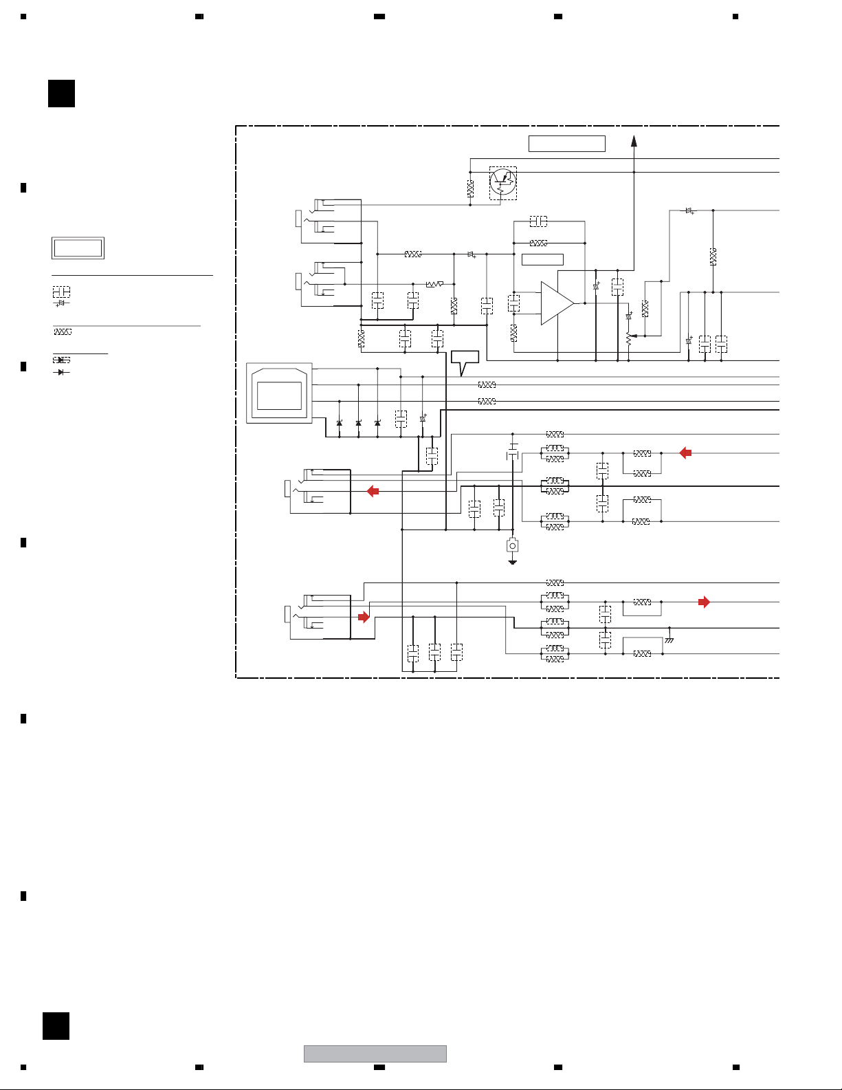
1234
3.7 HP 2 ASSY
A
HP2 ASSY
E
(XWZ4035)
NOTES
ALL CAPACITORS ARE IN µF
B
UNLESS OTHERWISE SPECIFIED
CH : CCSRCH
AL : CEAL (OTHER : CEAT)
TS : CE *-TS
ALL RESISTORS ARE IN Ω
RS1/16S***J
ALL DIODE
:1SS355
:1SS133
C
D
(OTHER : CKSRYB)
MIC (MAIN)
JA9401
AKN7005-
MIC (SUB)
JA9402
AKN7005-
JA9903
XKN3016
1
VBUS
2
D-
3
D+
4
GNDD
HP
5
4
2
3
7
8
1
JA9902
AKN7005-
FRONT AUDIO
5
4
2
3
7
8
1
JA9901
AKN7005-
5
4
2
3
7
8
1
5
4
2
3
7
8
1
D9901
R9429
D9902
UDZ6.8B
UDZ6.8B
(FAL)
C9428
STBY
D9903
(FL)
100pF
C9946
STBY
CH
C9427
C9430
0.01
0.1
C9947
C9943
1000p
R9425
3.3k
CH
100pF
C9429
47/16
C9948
C9944
TS
0.1
R9422
0.1
STBY
AL TS
C9426R9423
2.2/503.3k
STBY
+5.1V
R9960
R9959
C9945
0.01
STBY
R9426
C9425
1000p
C9953
KN9901
VNF1084-
GNDC
STBY
0
0
C9955
C9954
C9424
R9421
0.01
0.1
R9948
L9941
R9945
L9943
R9947
L9942
R9946
RT1P431MQ9401
C9423
R9420
21.5dB
2
-
3
STBY
+
IC9402(1/2)
10k
HA17558AF-
R9958
L9951
R9955
L9953
R9957
L9952
R9956
MIC AMP
1000p CH
39k
8
1
4
68
STBY
STBY
STBY
STBY
STBY
STBY
68
STBY
STBY
STBY
STBY
STBY
STBY
C9413
C9951
C9952
C9941
C9942
STBY
C9412
AL
0.022
0.022
220p
220p
C9422
VA+12V
0.1
2.2/50
VR9401
XCS3007-
R9951
68
R9953
68
R9954
68
R9952
68
R9943
STBY
R9944
STBY
STBY
R9419
C9421
2.2/50
GNDA
AL
TS
C9420
47/16
(FL)
(FAL)
R9418
C9436
0.1
47k
C9419
100p CH
E
F
E
28
1234
XV-HA5
Page 29
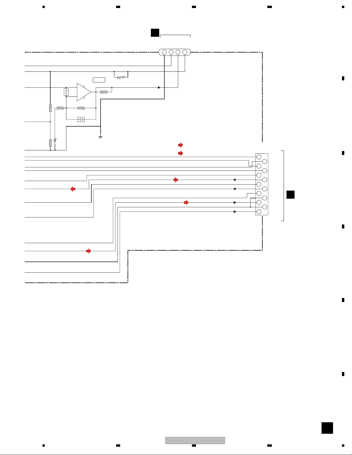
5678
CN5105
K
KARAOKE ASSY
A
GNDA
MIC
MIC SW
VA+12
243 1
J9911
D20PYY0435E
51048-0400
R9416
R9417
3.3k 3.3k
R9415
2.2k
C9416
2.2/50 TS
IC9402(2/2)
HA17558AF-
5
STBY
6
R9414
C9415
C9414
1200p
(FL)
12k
R9413
STBY
R9412
STBY
MIC
16.2dB
4
+
7
-
8
B
GNDA
:FLch AUDIO SIGNAL ROUTE
(FL)
:FA LCH AUDIO SIGNAL ROUTE
(FAL)
(FL)
(FAL)
CN9421
52045-1345
13
12
11
10
9
8
7
6
5
4
3
2
1
V BUS
D+
D-
GNDC
HPDET
HPL
GNDHP
HPR
FADET
GNDA
FA L
GNDA
FA R
CN5921
D
C
(FAL)
D
E
F
56
XV-HA5
E
29
7
8
Page 30
1234
3.8 REGULATOR and POWER ASSYS
REGULATOR ASSY
F
(XWZ4039)
W102
0
UVP+8
STBY
A
R52
Q81
W105
STBY
IRF9530
W101
+16.5V
R42
STBY
R44
STBY
R46
STBY
R48
STBY
STBY
S
D
W103
W106
G
B
100k
R81
R83
100
R41
STBY
R43
STBY
R45
0
STBY
R47
STBY
R49
STBY
R58
R59
STBY
STBY
Q53
D81
Q51
STBY
UDZS18B
R84
R82
STBY
STBY
C
R54
STBY
NJM78L05A
IC51
R55
(1%)
470
+4.9V
1/50
10/50
C54
C51
D
C55
STBY
Q54
2SC1740S(RS)
(1%)
470
R51
R61
1.8k
(1%)
STBY
C53
C56
R57
D3654 D3653
GNDPRE5
R3669
STBY
1SR154-400
+11.6V
D3656
D3658
KM200SA2L
CN3651
1
E
F
F
+
2
-
FAN MOTOR
R3659R3666
GNDFAN
C3654
33
33
R3665 R3670
0.022
C3653
22/50
R3658
47k
R3661
33k
Q3655 D3665
DTC114TK
33
33
R3660
C3652
FAN LOCK, SHORT, OPEN DETECT
D3664
10
100/10
10K
R3662
STBY
R3677
22k
30
+8.4V
STBY
STBY
STBY
D3655
R3678
STBY
W107
6.8k
(1%)
C52
R56
Q3654
2SC2412K(RS)
22k
XV-HA5
VPRE+5
SHORT DETECT(FAN+B,VP+8V,VP+15V)
Q71
2SA1037K(RS)
R71
0
47k
R74
D73
D71
D74
R78
4.7k
4.7k
D3651
Q3651
2SB1237X
D72
R77
47/25
R76
D3652
R3681
C3655
STBY
390 390
R3664
390
R3663
390
R3657
390
R3651
C3656
47/35
Q3653
2SC2412K(RS)
STBY
22
R3655
Q3652
2SC2412K(RS)
R3652
R3653
D75
4.7k
4.7k
R3654
D77
R3656
220
680
R3679
R3667
D3657
10k
1YF
C71
680
10k
R75
R73
R3680
1/50
100
470k
+B
R72
STBY
R3668
C3651
CN3303
KM250NA10L
1
2
3
4
5
6
7
8
9
10
47K
UVP+8
VP+8
SENSE5
GNDVP+8
VP+15
H/L CONT
REF5V
XPROTECT
FAN GND
+B
CN22
H
1234
Page 31

5678
NOTES
ALL CAPACITORS ARE IN µF
UNLESS OTHERWISE SPECIFIED
ALL RESISTORS ARE IN Ω
NO MARK DIODE
CH : CCSRCH
YF : CKSRYF
(OTHER : CKSRYB)
CEAT***M##-TS
:1/16W
1SS355
CN3301
KM250NA5L
L+OUT
L-OUT
CN24
GNDP
H
R-OUT
R+OUT
+B
+B
GNDP
GNDP
H/L CONT
GNDVP+15
VP+15V
CN23
SENSE
H
(VP+15V)
REF5V
MUTE
STBY
GNDA
RIN
GNDA
LIN
CN3302
KM250NA15L
5
4
3
2
1
15
14
13
12
11
10
9
8
7
6
5
4
3
2
1
2SA1037K(RS)
Q3656
R3676
R3674
+B
+26.8V
47k
R3307
STBY
GNDA
POWER ASSY
G
(XWZ4040)
D3659 R3671 IC3301
D3660 R3672
47k
R3675
4.7k
1k
1k
R3673
R91
100k
R65
220
C64
Q3304
2SC2412K(RS)
R3311
R3314
C3305
1k
POWER AMP
1k
R66
(1%)
R3301
R3302
R67
STBY
STBY
C65
W126
STBY
0
+15.8V
6.8k (1%)
D3304
IRF9540A
Q62
D
S
G
UDZ18B
R92
R93
0
100
D91
Q63
2SC2412K(RS)
R68
STBY
2.2k
R3312 R3313
10k
47
22/50
C3307
Q3305
RT1N241M
STBY
STBY
R3308
STBY
Q3303
VP
C61
47/25
C63
STBY
10k
UDZ4R7B
0
R3303
STBY
R3304
STBY
Q3302
C62
STBY
+4.2V
C3306
10/50
Q3301
STBY
STBY
L IN
DIAGNOSTIC OUT
MODE
12910
13
11
STBY
R3309
C3308
C3359
STBY
VP
STBY
C3351
C3353
R3351
R3319
0.47/50
STBY
R3305
STBY
R3306
0.47/50
L+ OUT
GNDP
8
C3361
STBY
0.1
0.1
10
STBY
C3301
R3320
STBY
C3302
L- OUT
7
C3362
STBY
C3355
C3357
R3353
GNDP
R- OUT
6
5
GNDP
C3360
STBY
0.1
C3356
0.1
C3358
101010
R3354
R3317
1k
R3318
1k
TDA8560Q
R+ OUT
4
+15.8V
C3310
R3310
C3309
0.1
C3352
0.1
C3354
R3352
C3303
C3304
VP
GNDA
2
3
100/25
10
0.01
0.1
0.1
2200p
2200p
R IN
1
+2.1V
C3311
A
B
C
0.01
D
E
F
:AUDIO SIGNAL ROUTE
XV-HA5
56
G
31
7
8
Page 32

1234
3.9 SECONDARY and PRIMARY ASSYS
A
B
CN22
KP250NA10
+B(FAN)
10
FANGND
REF5V
H/LCONT
VP+15
GNDVP+8
SENSE
(VP+8)
VP+8
UVP+8
CN23
GNDP
GNDP
H/LCONT
VP+15V
SENSE
(VP+15V)
REF5V
MUTE
STBY
GNDA
RIN
GNDA
9
8
7
6
5
4
68k(F)
3
2
1
15
+B
14
+B
13
12
11
10
9
8
39k(F)
7
6
5
4
3
2
1
LIN
XPROTECT
CN3303
C
D
F
KP250NA15
GNDVP+15
CN3302
G
SECONDARY ASSY
H
(XWZ4042)
R60
GNDP
R99
+7.8V
CN24
KP250NA5
1R-2
R+
G
354
L-
GNDP
CN3301
B1
VEF1040-A
PCB Binder
KN2
VNF1084-
CHASSIS_GND
D56
1SS355-
5234178119106423187510961112
L-
L+
L+
GNDP
R-
R+
(1/2)CN42
C
VP+15
MUTE
LIN
XPROTECT
GNDA
R94
47
51048-1100
D20PYY1125E
D20PYY1225E
J21
RIN
51048-1200
J22
VP+8
VP+8
VA-12
GLED
C
R95
4.7k
AC
UN+56
SYSPOW
(1/2)CN43
VA-12
GNDD
Q92
2SC4081
R96
10k
GNDD
GNDM
GNDM
GNDU
E
NOTES
ALL CAPACITORS ARE IN µF
UNLESS OTHERWISE SPECIFIED
CH :CCSRCH
:CEAL
AL
(OTHER :CKSRYB)
:CEAT
ALL RESISTORS ARE IN Ω
ALL INDUCTORS ARE IN µH
:CQMA
M
1/16W(CHIP)
LCYA
F
H
32
1234
XV-HA5
Page 33

5678
A
+26.8V
AKR7001
C45
*
IC31
TA79012S
OUT IN
C33
47/16
C22
4700/35
Q91
2SA1576A(QR)
+20.9V
D5SBA20(B)
D41
+
-
GNDD
GNDM
*FU2
H8
+21V
13
2
C32
0.047
S1WB(A)60SD-
4700/35
R53
15k
1SS355-
C41
6800/25
H7
AKR7001
1000/25
C31
D5SBA20(B)
C21
DAN202K-
C57
1/50 AL
D51
D55
UN+56
+16.5V
B6P-VH
CN21
W1
IC32
STBY
-
+
D31
D21
-
+
*
C25
R97
1k
51048-0500
D20PYY0520E
R98
1k
1
2
3
4
5
6
5
4
3
2
1
J11
UN+56
GNDU
AC
SYSPOW
HELP
* T2
SUB2
SUB2
SUB1
SUB1
MAIN
MAIN
115
115
CN3
0
0
52147-0510
CN26
UN+56
GNDU
SYSPOW
HELP
B5P9-VH
AC
PRIMARY ASSY
5
4
3
2
1
STBY
DAN217D15
1k
R13
C11
5
4
3
2
R85
1
56(1W)
UDZS16B-
R19
R18
470
2SD1664(PQR)-
D13
10
12
R12 R11
12
Q11
C12
1000/25
STBY
D12
S1WB(A)60SD-
+12.4V
D14
1SR154-400-
Q12
W224
W225
D11
XSR3011-
1SS355-
2SD1859X(QR)-
5
6
-
+
7
8
9
SPECIFICATIONS TABLE
* FU1
* FU2
* T1
* T2
* L1
* C25
* C45
RY1
4
3
2
1
*T1
WL/NT230V LF
800mA/250V
(REK1021)/J
5A/250V
(REK1029)/J
ATT7080ATS3098
XTF3003-
0.033/250V
0.033/250V
(XWZ4041: WL,NT)
I
(XWZ4044: LF)
W223
W222
W219
W220
W221
C3
0.01
ACG7033-
W201
W202
STBY
C2
*
W203
W204
1.6A/250V
(REK1024)/J
5A/250V
(REK1029)/J
ATT7080XTS3098
XTF3003-
W212
W214
W213
W208
NEUTRAL
ACE7013-
0.01 XKP3084-
C1
H1 H2
L1
*FU1
H1-H2:AKR7001-
H3-H6:STBY
110V
VNE1948-
W206
LIVE
W218
AN1
2
1
W211
KN1
B
312
S2
STBY
C
D
(DVDL)
XV-HA5
56
:AUDIO SIGNAL ROUTE
:DVD Lch AUDIO SIGNAL ROUTE
7
E
F
IH
33
8
Page 34

1234
3.10 KARAOKE ASSY
A
B
C
LOUT
GNDA
ROUT
GNDA
DVDR
GNDA
DVDL
GNDA
FRIN
GNDA
FLIN
VA+12
KEYCONSTB
KEYCONCLK
KEYCONDATA
ECHOVOL
VOCAL A
VOCAL B
VOCAL C
GNDU
GNDU
CN3101
1/2
C
CN8301
XKP3081-
2
4
6
8
10
12
14
16
18
20
DVDR DVDL
1
3
5
7
9
11
13
15
17
19
21
LOUT
ROUT
R8534 R8533
6.8k 6.8k
C8532 C8531
680p 680p
R8532
2.2k
ECHOVOL
2.2k
R8531
FLIN
FRIN
GNDA
(VOC)
R8303
R8302
R8301
R8304
2.7k
R8311
C8303
C8302
C8301
R8305
22k
C8311
680
C8304
0.22
47k
47k
47k
C8305
0.1
0.1
0.1
R8307
2.7k
C8315
STBY
2.2/50
C8306
0.047
RIN
9
10
11
12
10/50
ROUT
13
14
15
16 1
BA3838F
VOCAL FADER
R8306
680
C8316
SW1
SW2
IC8301
STBY
LIN
R8317
8
7
6
5
4
3
2
GND
REF
LOUT
MIC IN
Vcc
C8313
22k
C8307
C8309
C8310
0.01
C8317
10/50
47/16
C8308
2.2/50
2.2/50
C8312
2.2/50
4.7/50
C8201
VA+12
47/16
R8308
C8202
10k
0.047
R8202
C8203
10k
C8204
0.01
0.01
(MIC)
R8203
C8205
R8204
10k
0.01
5.6k
C8218
R8205
R8201
10k
0.01
10k
470p CH
C8217
R8206
R8209
R8208
R8207
10k
C8216
R8217
15k
C8206
8200p
4.7k
15k
6.8k
4700p
D
DVD MODULE
E
CN902
1/2
B
F
K
34
FR
Cr/R
Cb/B
CY/G
P/XI
27
26
FL
25
24
23
22
R
21
20
B
19
18
G
17
16
15
14
13
12
11
SY
10
9
V
8
7
6
SC
5
4
3
2
1
C8501
1000/6.3
C8502
1000/6.3
R8507
150(F)1/10W
150(F)1/10W
R8501
R8502
150(F)1/10W
150(F)1/10W
R8509
R8511
STBY
R8503
R8504
R8505
C8504
C8503
STBY
STBY
R8506
C8505
STBY
75(F) 0
GNDC
0
0
JA8502
D
34
YC
NoAssign1
AKB7146-
2
1
5
GNDA
GNDA
GNDD
GNDD
GNDD
GNDD
GNDD
GNDD
GNDD
GNDD
GNDD
ASPECT
VSEL1
VSEL2
SQUEEZE
CN8502
VKN1258-
NOTES
ALL CAPACITORS ARE IN µF
UNLESS OTHERWISE SPECIFIED
CH :CCSRCH (OTHER :CKSRYB)
:CEAL
AL
:CEAT
ALL RESISTORS ARE IN Ω
1/16W(CHIP)
ALL INDUCTORS ARE IN µH
LCYA
XV-HA5
1234
Page 35

VA+12
L8201
STBY
5678
R8216
2.2k
R8218
Q8201
2SD1858X(QR)
STBY
2.2k
R8220
R8215
KARAOKE ASSY
K
(XWZ4043)
10
A
6.8k
R8211
C8219
C8215
0.22
C8214
0.22
R8210
C8220
1000p
IC8201
4.7k
MIX OUT Vcc
15
MIX IN
16
LPF2OUT
17
1200p
LPF2IN
18
HPFOUT
19
HPFIN
20
LPF1OUT
21
LPF1IN
22
ADINT IN
23
ADINT OUT
24
DAINT IN KEYDOWN
25
DAINT OUT
26
MODE1
27
MODE2 ADCONT
28
M65847AFP-
C8221
10/50
STROBE
KEY CON
DACCONT2
DACCONT1
GND
REF
KEY5
KEY4
SCK
SDATA
CLKO
KEYUP
D8201
14
13
12
11
10
9
8
7
6
5
4
3
2
1
UDZS5R6B
C8222
C8223
0.047
C8213
C8212
R8214
C8211
R8213
R8212
C8210
C8209
C8208
C8207
47/16
AL
47/16
AL
1k
STBY
1k
1k
STBY
0.068
0.068
0.068
MIC ECHO
IC8401
116
GND
ECHO VR
C8434
C8410
0.47
C8407
CH100p
0.01
R8409
10k
R8408
4.7k
R8407
15k
C8411
0.01
C8408
Q8402
2SJ103(GR)
2
STBY
BIAS
314
DAINT IN
4
DAINT OUT
5
DALPF IN
6
7
DALPF OUT
89
3300p
22/16
C8409
AL
(MIC)
C8432
2.2/50
S
D
22k
R8434
BU9255FS
CR
15
MUTE
Vcc
13
ADINT IN
12
ADINT OUT
ADLPF OUT
ADLPF IN
MIX INMIX OUT
C8433
G
0.22/50
R8432
1M
1M
R8431
C8404
11
10
C8406
R8405
20k
C8431
2.2/50
VA+12
(MIC)
0.01
R8404
4700p
8.2k
R8406
C8403
20k
R8402
39k
100p
R8403
C8402
10k
C8405
0.012
0.1
L8401
C8401
STBY
100/16
B
C
MIC
MIC SW
J9911
CN5105
52147-0410
VA+12
HP2 ASSY
4132
GNDA
E
D
E
F
56
XV-HA5
K
35
7
8
Page 36

1234
3.11 WAVEFORMS
Note : The encircled numbers denote measuring point in the schematic diagram.
DVDM ASSY
B
A
Measurement condition ;
No. 1 to 10 : reference A1 (DVD), T2-chp 19, Color-bar
No. 11 to 14 : reference A1 (DVD), T1
IC201-pin47 [FG]
1
V: 1V/div. H: 2msec/div.
B
IC201-pin 39 [TROPENPWM]
2
V: 1V/div. H: 5µsec/div.
[Tray stops]
[Tray is opening] [Tray is closing]
GND
GND
GND
GND
C
IC201-pin37 [DMSO]
3
V: 1V/div. H: 10µsec/div. V: 1V/div. H: 10µsec/div. V: 1V/div. H: 2sec/div.
D
CN102-pin 11, 10, 9 (IC101-pin 14, 13, 12)
4
[SPINDLE (WVU)]
V: 2V/div. H: 2msec/div.
[TRAY OPEN] [DVD PLAY] [DMSO]
GND
GND
GND
PLAY
Pless OPEN key Pless PLAY key
Braking a turn of disc
IC201-pin225 [ASPDIF AUDIO DIGITAL SIGNAL]
11
V: 2V/div. H: 500nsec/div.
Tray :
opening
GND
GND
E
IC401-pin23 [CompositeVideo Out]
8
V: 1V/div. H: 10µsec/div.
GND
F
36
IC401-pin21 [S VIDEO OUT - Y]
9
V: 1V/div. H: 10µsec/div.
IC401-pin26 [S VIDEO OUT - C]
10
V: 1V/div. H: 10µsec/div.
XV-HA5
9
9
10
GND
10
GND
1234
Page 37

5678
Note : The encircled numbers denote measuring point in the schematic diagram.
IF ASSY
C
SYSTEM Microcomputer(IC)<–>Each part communication waveform
A
IC5501-pin 25 [SCLK0]
1
V: 2V/div. H: 20us/div.
IC5501-pin 28 [LCDCLK]
4
V: 2V/div. H: 5us/div.
[ANY FUNCTION]
IC5501-pin 51 [SCLK2]
10
V: 2V/div. H: 10us/div.
[MD]
[DVD]
IC5501-pin 23 [SDATA0]
2
V: 2V/div. H: 20us/div.
IC5501-pin 26 [LCDDATA]
5
V: 2V/div. H: 5us/div.
IC5501-pin 49 [SDATA2]
11
V: 2V/div. H: 10us/div.
1
GND
2
GND
4
GND
5
GND
IC5501-pin 25 [SCLK0]
1
V: 2V/div. H: 20us/div.
IC5501-pin 46 [VOLCLK]
6
V: 2V/div. H: 100us/div.
[VOL UP/DOWN]
IC5501-pin 51 [SCLK2]
10
V: 2V/div. H: 10us/div.
[MD]
[DVD]
IC5501-pin 23 [MDATA0]
3
V: 2V/div. H: 20us/div.
IC5501-pin 45 [VOLDATA]
7
V: 2V/div. H: 100us/div.
IC5501-pin 50 [MDATA2]
12
V: 2V/div. H: 10us/div.
1
GND
3
GND
6
GND
7
GND
IC5501-pin 48 [SELCLK]
8
V: 2V/div. H: 50us/div.
[FUNCTION CHANGE]
IC5501-pin 47 [SELDATA]
9
V: 2V/div. H: 50us/div.
8
GND
9
GND
B
C
IC5501-pin 61 [TXCLK]
13
V: 2V/div. H: 100us/div.
DISP ASSY
D
[TUNER]
14
USB Interface data waveform
10
GND
11
GND
IC5501-pin 62 [TXODATA]
V: 2V/div. H: 100us/div.
13
GND
14
GND
IC5501-pin 61 [TXCLK]
13
V: 2V/div. H: 100us/div.
IC5201-pin 1 [D+]
1
V: 2V/div. H: 500us/div.
[USB (At connecting PC)]
[TUNER]
IC5501-pin 66 [TXIDATA]
15
V: 2V/div. H: 100us/div.
IC5201-pin 2 [D-]
2
V: 2V/div. H: 500us/div.
10
GND
12
GND
13
GND
15
GND
1
GND
D
E
2
GND
XV-HA5
56
F
37
7
8
Page 38

1234
A
B
C
D
E
F
38
1234
XV-HA5
Page 39

5678
4. PCB CONNECTION DIAGRAM
NOTE FOR PCB DIAGRAMS :
1. Part numbers in PCB diagrams match those in the schematic
diagrams.
2. A comparison between the main parts of PCB and schematic
diagrams is shown below.
Symbol In PCB
Diagrams
BCE
BCE
D
Symbol In Schematic
Diagrams
BCEBCE
BCE
DGGSS
BCE
DGS
Part Name
Transistor
Transistor
with resistor
Field effect
transistor
Resistor array
3-terminal
regulator
3. The parts mounted on this PCB include all necessary parts for
several destinations.
For further information for respective destinations, be sure to
check with the schematic diagram.
4. View point of PCB diagrams.
Connector
P.C.Board
Capacitor
Chip Part
A
SIDE A
B
SIDE B
4.1 LOAB ASSY
SIDE A SIDE B
LOAB ASSY
A
LOAB
12
VWG2279VWG2346-
1
CN601
CN602
VNP1836-C
S101
5
51
VWG
5
(VNP1836-C)
LOAB ASSY
A
PNE-1B1
GND
(VNP1836-C)
(V+5D)
V+3D
15
SW2
C102
C101
51
LOAD+
LOAD-
CN601
CN602
C
D
E
CN601CN602 CN601 CN602
CN104
M
LOADING MOTOR
ASSY
B
A A
56
XV-HA5
7
8
F
39
Page 40

1234
4.2 DVDM ASSY
A
B
DVDM ASSY
SIDE ASIDE A
To STEPPING MOTOR
To SPINDLE MOTOR
CN102
CN103
B
C
IC561
Q701
Q702
Q304
IC761
Q305
Q562
IC751
Q564
IC101
IC731
Q565
Q561
Q881
Q308
Q533Q534
Q731
Q801
Q307
IC531
Q535
Q532
Q531
IC711
Q506
CN901
CN5952
C
CN101
To PICKUP ASSY
Q503
Q502
Q401
Q504
IC591
IC501
IC204
Q501
Q505
IC201
Q851
Q821
Q481
A
CN104
CN601
CN8502
K
CN902
(ANP7527-A)
D
E
F
B B
40
1234
XV-HA5
Page 41

5678
DVDM ASSY
B
SIDE BSIDE B
A
B
Q732
Q201
IC203
IC451
IC202
C
D
E
IC401
(ANP7527-A)
B B
56
XV-HA5
7
8
F
41
Page 42

1234
W269
SPDIF
LITTELFUSE INC
4.3 IF ASSY
A
B
C
D
SIDE A
IF ASSY
C
IC301
IC8881
OPT-I
OPT-O
JA4601
JA4602
JA3001
W203
W172
W138
C4621
C4603
AUXI(R)
W139
W140
W141
AUXO(L)
W204
OUT
IC301
IN
AUXO(R)
W121
C302
B1
C3312
C3309 C3310 C3311
SIDE
PRINTED
TA7812S
IC3301
CN42
CN8301
K
TUNER MODULE
M
CN3101 CN5701
11.GND
7.+9V
6.TXL
8.TXR
CN5701
W179
XSYSMUTE
W127
CN43
5.GND
4.DO
3.CLK
21
W229
W180
W181
W147
XPROTECT
W129
W128
1
2.DI
W261
W145
1.CE
AUXI(R)
W230
W182
W130
W107
1
CONTACT
W262
AUXI(L)
W183
VUN+56
W131
AC
SIDE
W231
TX(R)
W132
W232
TX(L)
W233
SYSPOW
OPEN
SIDE
W133
W213
W209
W211
W184
W185
W263
1.VA-12
W148
W134
VP+8
W264
2.VP+8
3.VP+8
4.GNDM
W212
IC3201
EVOLCLK
W149
EVOLDATA
GNDU
12
49102.5
GNDD
OPTIN
GNDM
W268
W266
W267
W265
CN3102
111
11.OPTOUT
10.OPTIN
9.OPTIN
8.GNDD
5.GNDM
6.GNDH
7.GNDD
B2
W210
CAUTION
MARKED.MFD BY
W295
C504
REPLACE IC LINKS AS
IC8881
10.RDS
W256
OPEN
SIDE
W206
W293
VTX+9
W142
W294
1
11
W207
W257
W208
W177
W176
W175
W174
W173
C3913
C3914
W122
W223
C3908
C3903
W106
GNDA
W224
W258
1
W228
C5711
C3907
IC3911
W227
W226
W225
C3258
C3257
C5712
W123
C3904
HP(L)
CN3101
IC3271
W178
W124
W259
W260
VA+12
MD(R)
MD(L)
DVD(R)
DVD(L)
W125
11
C3912
C3911
HP(R)
9.VSM
W146
HPMUTE
W126
CN42
C3281
E
CN3352
W104
W103
W101
W102
C3284
BOND
BOND
F
BOND
C3282
C3283
BOND
W105
BOND
FCICT
PRODUCTION CODE
IF ASSY
LF
H
J21
CN43
H
J22
R
C
42
1234
XV-HA5
Page 43

5678
3
W133
ULE
SIDE A
A
C3026
W191
W276
USB(L)
W236
W195
W194
GNDU
W165
UTEST
W158
C3191
W193
W159
W280
W279
W278
W277
W237
W238
W243
W242
W241
W240
W217
W192
VE+5
STEST
W160
W244
W161
W136
W162
W281
W239
W163
W282
IC5501
C3930
W164
CONTACT
SIDE
W137
W283
1
W166
CN51
1.WEN/DI
2.WD0
3.WCLK
W167
W168
4.RST
5.VCC
W196
6.VSS
W218
7.NC
7
W245
W169
X5502
W197
W284
W285
X5501
W252
W251
W250
W249
W248
W247
W291
W219
FA(L)
C3021
W274
C3242
C5805
W275
USB(R)
C3022
R3232
W111
C3192
W235
W216
W215
W214
W190
W189
XDVDRST
IC3191
C3025
W157
W156
W155
W154
W153
GNDD
OPTIN
VP+8
GNDM
W263
W264
W265
OPEN
CN3102
SIDE
1.VA-12
2.VP+8
3.VP+8
5.GNDM
6.GNDH
4.GNDM
W213
W209
W211
W184
W185
W148
W134
W212
IC3201
EVOLCLK
W149
EVOLDATA
GNDU
W210
SPDIF
W270
W268
W269
W266
W267
111
11.OPTOUT
10.OPTIN
9.OPTIN
8.GNDD
7.GNDD
W234
B2
C3254
C3253
W188
W187
W186
VA+12
W151
CAUTION
W295
REPLACE IC LINKS AS
C5804
MARKED.MFD BY
LITTELFUSE INC.
C504
C5809
W271
W152
W135
VA-12
W272
FA(R)
R3233
C3241
W273
GNDA
IC3001
C5801
12
W288
W287
W253
W220
W286
W289
1
29
W290
CN5951
W221
W198
W170
1.DIMMER
2.GLED
3.TMRLED
4.VP+12
5.XLCDRST
6.LCDCLK
7.LCDCS
8.LCDDATA
9.VE+5
10.VESW+5
11.GNDD
12.GNDU
13.REMOCON
14.KEY1
15.KEY2
16.SUSPEND
17.USBL
18.GNDA
19.USBR
20.HPDET
21.GNDA
22.HPL
23.GNDHP
24.HPR
25.FADET
26.GNDA
27.FAL
28.GNDA
29.FAR
SIDE
CONTACT
W255
HP(L)
HP(R)
W254
W222
GNDHP
W292
W202
W200
W199
W201
W171
(XNP3094-B)
CN5951
B
CN5911
D
C
49102.5
CN43
H
J22
IC8881
C8885
W108
W109
GNDM
H:6
GNDH
W110
GLED
W112
XCLK2
W113
MDATA2
W114
DVDACK
W115
SDATA2
W116
VDET
W117
SYSCS1
W118
DVDON/OFF
CONTACT
SIDE
CN5952
W119
CN5952
B
W120
CN901
251
D
E
F
56
XV-HA5
C
43
7
8
Page 44

A
N
XPROTECT
5 GND
0
18 SYSC1
2
N
SIDE B
1234
IF ASSY
C
C
R3071
R3072
5.VCC
3.WCLK
4.RST
6.VSS
7.NC
2.WD0
1.WEN/DI
R5502
R5510
R5501
C5523
R5598
R5602
R5523
C5598
R5626
R5698
R5509
R5524
R5693
R5512
R5525
CN51
R5600R5599
R5593
C5589
100
1
R5526
7
C5514
R5527
R3935
R3934
Q5831
R5592
R5585
R5528
Q3951
R3933
1020
CN5951
C5518
C5519
1
29
C5522
C5509
C5510
R5622
15.KEY3
C5502
R5623
1.DIMMER
2.GLED
3.TMRLED
4.VP+12
5.XLCDRST
6.LCDCLK
7.LCDCS
8.LCDDATA
9.VE+5
10.VESW+5
11.GNDD
12.GNDU
13.REMOCON
14.KEY1
GNDHP
R5519
R5522
20.HPDET
R5932
R5933
21.GNDA
15.KEY2
16.SUSPEND
17.USBL
18.GNDA
19.USBR
22.HPL
23.GNDHP
24.HPR
25.FADET
26.GNDA
27.FAL
28.GNDA
29.FAR
R5601
B
CN5951
HPL
HPR
R5508
R5507
C5507
R5617
C5517
C
R5515 R5615
R5517
R5518
(XNP3094-B)
D
C8881
C8883
25
R8881
CN5952
R5529
R5531
L8881
1
R5832
81
R5530
D3001
Q3003
R5831
Q5832
R5532
R5533
R5595
R5590
30
R5534
R5536
D3953
R3010
80
R5635
R5573
R5535
R5624
R5572
R5537
R3939
C8884
R5625
R5570
31
R5594
R3936
C8882
R5576
IC5501
Q3953
C5540
Q5804
C3931
Q3952
25.VDVD+12
R5643
R3938
VPR+8
R5567
C5555
R5644
D3951
1
VPR+8
51
50
C5597
C5596
R3937
VPR+8M
VPR+8M
R3293
GNDM
20.GNDM
R5565
R5564
STEST
C3932
GNDD
GNDD
R5562
R5563
R5568
R5566
R3194
R5578
R5577
R5551
R3044
R3045
R3046
Q3043
R5808
R5543
UTEST
SYSCS1
15.GNDD
DOUT
USB(L)
R5561
R5579
C3194
R3196
R5557
Q3042
R3043
R3047
R5597
R5574
VDET
GNDD
DVDPOWER
R3193
58
R3030
Q3041
R5591
DVDACK
SDATA2
10.SCLK2
XDVDRST
XREADY
R3195
C3195
14
C3193
R3191
IC3191
R3029
R3042
R3041
R5596
R5544
R5542
R5575
R5550
R5549
Q5801
D5801
XCLK2
MDATA2
VDET
SDATA2
MDATA2
ACK
GNDD
5.GNDD
GNDA
FA(L)
USB(R)
FA(R)
R3197
R3198
C3196
R3192
IC3001
16
17
R5801
NC
R3036
NC
1
C3017
R3035
R3027
R3028
D3222
D3221
Q5802
D5802
R5802
C5806
GNDM
GNDH
GLED
R5807
Q5803
C5808
R5806
MARKED.MFD BY LITTELFUSE INC.
1.NC
SPDIF
CN3102
R8882
9.OPTIN
10.OPTIN
11.OPTOUT
R3011
R3012
R3250
C3040
C3018
L5801
C3039
R3040
C5802
R5804
C3019
R3039
C3244
C5803
C3243
R3249
C503
IC501
R3262
2140
32
R5803
C5807
49102.5
CAUTION
R5805
REPLACE IC LINKS AS
OPTIN
8.GNDD
C3202
R3210
R3261
C3209
C3211
IC511
GNDD
7.GNDD
6.GNDH
C3207
C3208
R3215
C3210
GNDM
5.GNDM
4.GNDM
C3206
R3214
C501
D511
VP+8
111
3.VP+8
2.VP+8
1.VA-12
R3217
R3218
C3201
R3209
120
EVOLCLK
EVOLDATA
GNDU
11.GNDM
12.GNDU
C5721
C5722
C5792
R3253
IC3201
C3245
9.GNDD
10.GNDM
C5723
TX(L)
C3251
C3204
R3211
R3213
8.GNDD
R3260R3256 R3258
SYSPOW
C5724
TX(R)
C3252
R3254R3252
R3257
R3251
R3255
R3928
R3930
C3203
R3212
R3931
R3932
AC
6.AC
7.SYSPOW
1.CE
1
21.GNDU
AUXIL
R3926
Q3903
R3924 R3923
VUN+56
5.UN+56
4.GLED
3.CLK
2.DI
CN57
20.GNDU
AUX(R
10.GNDA
R3259
R3922
R3920
R3929
3.VA-12
4.DO
19.SYSC2
9.FRIN
R3918
R3912
P
R3927
2.VP+8
CN43CN5952
E
F
C
44
1234
XV-HA5
Page 45

R3209
C3201
EVOLDATA
12
GNDU
VP+8
3.VP+8
2.VP+8
R3217
R3218
C5722
1
1.VA-12
1
40
EVOLCLK
GNDU
C5721
C5792
R3253
IC3201
C3245
R3213
C5723
TX(L)
R3260R3256 R3258
C3251
C3203
C3204
R3212
R3211
SYSPOW
C5724
TX(R)
C3252
R3254R3252
R3255
R3930
R3257
R3251
R3928
R3931
R3932
AC
R3923
R3924
1.CE
1
CN5701
21.GNDU
AUXIL
10.GNDA
R3926
R3922
Q3903
VUN+56
CN5701
4.DO
3.CLK
2.DI
6.TXL
5.GND
20.GNDU
17.XMDRST
18.SYSC1
19.SYSC2
21
AUX(R
9.FRIN
8.GNDA
(JJ)
R3259
R3918
R3912
R3920
R3925
R3929
R3927
XPROTECT
5678
SIDE B
A
CN3101
Q5711
8.TXR
7.+9V
15.MDATA0
16.SCLK0
5.DVDR
7.DVDL
6.GNDA
C3271
R3278
C3272
R3272
Q3293
R3917
XSYSMUTE
9.VSM
10.RDS
11.GND
11.FLIN
12.VA+12
14.SDATA0
13.SPDIFPOW
1.MDR
4.GNDA
2.GNDA
3.MDL
C3273
R3271
R3277
IC3271
58
C3276
C3274
NP NP
Q3901
R3921
R3919
R3911
HP(R)
HPMUTE
11
DVDL
R3274
C5713
MDR
D5713
VA+12
R3031
R3032
CN3101
MDL
DVDR
R3051
R3049
R3273
C3275
R3276
R3275
14
Q3291
R3264
C3277
R3263
Q3292
R3279
C3910
R3910
C3906
IC3911
14
HP(L)
R5712
R3033R3034
58
R3906
R3908
R3907
R5711
1
R3050
R3048
C3278
D5711
GNDA
1.MDR
(JJ)
19.VOCALC
18.VOCALB
9.FRIN
8.GNDA
10.GNDA
C3915
C3916
R3909
D3225
C5793
15.KCDATA
16.ECHOVOL
17.VOCALA
5.DVDR
6.GNDA
7.DVDL
(GEN)
R3915
R3913
R3916
R3914
C3909
R3905
C3905
R3226
11.RIN
C5795
C5794
21.GNDU
12.VA+12
13.KCSTB
14.KCCLK
2.GNDA
3.ROUT
4.GNDA
VTX+9
9.LIN
10.GNDA
C5791
20.GNDU
11.FLIN
1.LOUT
C3301
R3303
R3301
C3302
R3302
6.VP+15
7.MUTE
8.XPROTECT
C3305
R3304
5.L+
R3309
C3306
4.L-
R3310
2.R-
3.GNDP
R3315R3316
C3303
IC3301
58
C3304
1.R+
IC301
OUT
IN
R3305R3306
R3307
1
14
C3308
C3307
R3308
R3313
R3314
AUXOR
R3019
Q4621
R3017
R3015
R3021
C301
C3009
R3022
R3020
R4623
C3006R3014
R3018
R4622
R4616
R3025
L3004
L3006
C3010
C4608
R4604
R4605
R4603
C3007
R3004
R3006
AUXOL
NP
Q4602
R4624
C4605
R3026
C3008
D4621
AUXIR
Q3001
Q4601
C3005
R3007
L3007
R3009
L3009
C4614
R3013
R3016
R4621
C4612
ROUT
R3008
R4601
LIN
LOUT
RIN
L3008
L4603
R3005
R4602
L3005
C3012
C3013
C4604
C4611
C4615
C3015C3016
IC3191
IC3001
IC5501
IC3201
IC501
IC511
IC3271
IC3301
IC3911
Q5711
Q4621
Q3291
Q3292
Q3001
Q3041
Q3042
Q3043
Q3293
Q5802
Q3903
Q3901
Q5801
Q5831
Q5832
Q3953
Q3951
Q5952
Q3003
B
C
6.AC
9.GNDD
10.GNDM
8.GNDD
5.UN+56
7.SYSPOW
4.GLED
3.VA-12
2.VP+8
.
11.GNDM
CN43 CN42
CN43
1.VP+8
R3225
R3234
Q3221
D3224
IF ASSY
XWZ4030
XWZ4033
1
0
123456789
0
0
123
1
0
D3223
XWZ4049
R
CN42
C3287
R3289
C3285
R3281
R3292
C3292
R3284
C3289
C3291
R3291
R3282
C3290
+
C3286
+
C3288
R3290
R3287
R3285
+
R3283
+
LF
A
B
C
XV-HA5
56
D
Q5803
Q3221
E
F
C
45
7
8
Page 46

1234
4.4 DISP ASSY
A
B
C
D
SIDE A
DISP ASSY
D
1
CONTACT
SIDEUPPER
C
CN5911
W613
W614
W615
W616
W617
W618
W619
W620
W621
CN5951
CN5911
W612
W622
V5901
SIDE A
CN9421
E
CN5921
CONTACT
SIDEUPPER
LF
W623
W625
C5216
C5215
W609
W628
W608
W630
W610
W626
J1
W624
W606
R
115
VOL+
S5963
W601
W602
W603
W604
FM/AM/LINE
S5955
IC5201
MD
S5954
S5953
DVD/CD
C5208
CN5921
VOL-
W605
13
S5964
S5957
S5962
S5961
29
W629
1
C5905
X5201
9
W611
C5942
DISPLAY ASSY
E
D5921
D5922
D5923
X5941
MD
S5952
ON/OFF
D5920
S5951
DVD/CD
S5956
D5924
(XNP3094-B)
F
D D
46
1234
XV-HA5
Page 47

5678
SIDE B
DISP ASSY
D
CN5921
15
CN5921
R5964
R5963
R5962
C5961
R5957
R5956
R5952
R5971
C5951
F
D
R5955
E
R5210
C5214
C5204
C5205
R5954
R5953
1
9.HPDET
8.HPL
Q5925
C5922
7.GNDHP
5.FADET
6.HPR
15.KEY3
14.GNDU
R5206
R5209
114
R5205
R5204
R5931
4.GNDA
3.FAL
13.VBUS
12.D+
IC5201
R5214
R5215
Q5921
2.GNDA
11.D-
R5924
R5923
1.FAR
10.GNDD
R5212
C
SIDE B
A
B
CN5911
R5982
VE+5
LCDDATA
LCDCS
LCDCLK
XWZ4034
R
Q5971
1
CN5911
GLED
TMRLED
1.DIMMER
R5981
VP+12
5.XLCDRST
XWZ4031
DISPLAY ASSY
IC5201
XWZ4045
LF
R5922
R5921
R5930
Q5923
Q5971
Q5922
Q5924
Q5921
Q5925
C
D
E
29
HPL
FAR
GNDA
HPDET
FAL
GNDHP
GNDA
A
L5201
C5901
C5902
C5207
C5206
R5202
D5901
C5201
R5213
C5210
C5213
NP
Q5924
D5927
D5925
R5203
Q5203
R5942
C5202
R5218
R5901
Q5202
R5219
R5941
R5943
1528
Q5201
C5217
R5216
R5217
GNDA
25.FADET
R5211
19
USBR
GNDA
HPR
USBL
KEY1
REMCON
GNDU
GNDD
15.KEY2
SUSPEND
10.VESW+5
R5911
C5903
R5902
R5903
R5904
R5905
R5906
C5941
R5951
R5961
B
R5927
R5929
R5928
R5910
C5910
C5907
D5907
C5908
R5909
C5909
D5909
Q5922
R5926
R5925
C5921
G
D5910
R5907
R5908
D5908
Q5923
H
(XNP3094-B)
D D
56
XV-HA5
7
8
F
47
Page 48

1234
4.5 HP2, REGULATOR and POWER ASSYS
4
SIDE A
A
1
J9911
J9911
CN5105
HP2 ASSY
E
K
W501
C9416
Q3651
VR9401
W504
Q81
C9421
B
REGULATOR ASSY
F
C
Q54
C9420
W514
W502
IC51
JA9401
C9422
C9413
MIC1
W503
IC9402
REGULATOR ASSY
Q3651
W125
C3652
FAN+
W110
GND FAN
JA9402
W505
MIC2
C3656
FAN+
GND FAN
W123
W124
R
W108
C3651
+B
W109
C9426
KN9901
W506
JA9902
HP
W507
JA9901
C9947
FA
R
W508
HP2 ASSY
USB
JA9903
W509
W510
LF
13.VBUS
12.D+
11.D-
10.GNDD
9.HPDET
8.HPL
7.HPGND
6.HPR
5.FADET
4.GNDA
3.FA(L)
2.GNDA
1.FA(R)
W511
W512
CONTACT
SIDE
CN9421
113
CN9421
CN5921
D
(XNP3094-B)
PRINTED SIDE
B
W106
W119
GNDPRE5
W120
W105
Q53
UPRE5V
W118
IRF9530
W101
SENS5V
W117
S
PRE5V
W116
D
W103
C52
G
PRE5V
W104
Q81
W102
Q54
Q51
E
C
W107
C55
REF5V
H/L CONT
W121
W122
IC51
C51
+B
OPEN
SIDE
10
CN3303
XPROTECT
FAN GND
REF5V
VP+15V
H/L CONT
SENSE5
GNDVP+8V
VP+8V
D
CN3303 CN3651
1
UVP+8V
C3654
+
-
1
BLACK
OPEN
SIDE
CN3651
RED
1
(XNP3095-B)
M
CN22
POWER ASSY
H
G
POWER ASSY
IC3301
R
W137
L+OUT
L-OUT
W138
W139
W140
GNDP
W141
R-OUT
E
OPEN
SIDE
Q62
F
CN3301
W115
L+OUT
L-OUT
W113
W114
GNDP
W129
R-OUT
W130
R+OUT
VP
GNDP
C3307
C3306
W136
W133
R+OUT
15
CN3301
Q62
GDS
PRINTED SIDE
IRF9540A
GNDP
W132
CN3302
15
C3310
13
W131
+B
15
LIN
W135
FAN MOTOR
PRINTED SIDE
VP
MODE
GNDP
L+OUT
L-OUT
R-OUT
DIAOUT
+B
VP
C61
GNDP
H/L CONT
GNDP
GNDP
C3305
PRE12V
GNDPRE12
CN3302
GNDP
R+OUT
W134
PRE12V
SENSE12
VP
W126
1
RIN
GNDA
W112
W111
OPEN
C3302
SIDE
REF5V
W127
MUTE
MUTE
RIN
IC3301
GNDA
STBY
W128
GNDA
C3301
GNDA
LIN
1
GNDA
RIN
(XNP3095-B)
CN24
E F G GFE
48
H
XV-HA5
H
CN23
1234
Page 49

5678
SIDE B
13 1
CN9421
7.HPGND
6.HPR
CN9421
5.FADET
4.GNDA
3.FA(L)
2.GNDA
1.FA(R)
HP2 ASSY
E
D9903
R9959
13.VBUS
R9960
12.D+
11.D-
10.GNDD
D9902
9.HPDET
8.HPL
REGULATOR ASSY
F
C9946
C9948
C9945
D9901
R9948
L9941
R9945
C9941
R9943
R9947
L9943
C9944
C9943
R9944
L9942
R9946
C9942
LF
R81
R83
C54
R51
R61
R55
D81
C53
C56
R56
C3653
+
C9954
C9953
C9955
Q54
R9958
L9951
R9955
R9953
R9951
C9951
L9953
R9957
Q81(Q52)
R57
-
L9952
R9956
C9952
REGULATOR ASSY
D
S
G
B
R58
R49
C52
Q53
R82
R54
UPRE5V
SENS5V
PRE5V
R52
PRE5V
C3654
UVP+8V
110
R48
R46
R44
R42
R84
R78
VP+8V
R9954
R9952
C51
GNDPRE5
SENSE5
C9427
R9425
C
R59
D74
R77
R9422
Q51
E
IC51
H/L CONT
R71
D72
GNDVP+8
VP+15V
C9428
R9423
R47
R45
R43
R41
R74
R75
5
C9429
C9430
R9429
REF5V
H/LCONT
Q71
C9425
R73
REF5V
R3655
R3652
R3679
R3680
Q3652
D77
R3656
R3667
I
OG
Q3654
D73
R72
XPROTECT
R
D3657
C55
R3677
D75
FAN GND
Q3653
R3668
D3665
D71
C71
+B
C9412
R9421
C9423
R9420
C9424
IC9402
1458
XWZ4039
+B
R3654
R3653
C3655
C3651
R3661
R3662
R3678
D3664
G FAN
R76
FAN+
D3658
R9413
C3656
D3656
FAN+
R3660
R3659
R9414
C9414
C3652
D3652
D3651
C9415
LF
Q3655
R3658
R3670
R3666
R3665
D3653
G FAN
D3654
GNDA
R
R3657
R3651
D3655
R9416
R9417
C9419
C9436
R9415
VA+12
R3681
R3664
R3663
R3669
(XNP3095-B)
J9911
HP2 ASSY
R9418
XWZ4035
R9419
(XNP3094-B)
Q3652
Q3653
Q3654
Q71 Q3655
41
Q9401
SIDE B
R9412
R9426
LF
A
B
C
D
CN3651 CN3303
POWER ASSY
G
5
R3309
R3310
R3307
GP
C3308
13
1
VP
RIN
Q3656
13
GNDA
R+OUT
VP
C61
C3310
R3313
D3304
Q63
15
SD
+B
GNDP
R3675
Q3305
R91
R-OUT
L-OUT
G
GNDP
D91
L+OUT
Q3304
10
VP
C3306
R92
MODE
R3673
DIAOUT
R3312
13
LIN
R3676
C3307
R3314
R93
D3659
R3671
R3311
R+OUT
1
R+OUT
1
R
C3303
POWER ASSY
XWZ4040
C3304
R3318
R3317
C3311
GNDA
MUTE
L
R3319
R3303
C3301
Q3301
R3301
R3305
R3302
Q3302
5
1
RIN
GNDA
LIN
STBY
GNDA
E F G GFE
GNDP
Q3303
R3308
R
R3306
MUTE
R3320
R3304
C63
REF5V
C3302
R67
SENSE
C3309
C3305
R65
C65
C64
R68
10
R66
C62
12
GP
H/L CONT
P12
G12
CN3302 CN3301
R3674
R3672
R-OUT
R-OUT
D3660
L-OUT
GNDP
L-OUT+BL+OUT
C3351
C3357
C3355
C3353
R3353
R3351
C3359
C3361
C3362
R3354
R3352
C3360
C3354
C3358
C3352
C3356
L+OUT
5
(XNP3095-B)
Q3656
Q3304
Q3305
Q63
XV-HA5
56
7
E
F
49
8
Page 50

1234
4.6 SECONDARY ASSY
A
B
C
D
E
SIDE A
IC31
SECONDARY ASSY
H
D21
GNDUGNDU
W24
W41
W37
W36
VP+15
W8
C25
C45
H8
HELP
GLED
W10
W9
A
C57
+B
W4
BOND
C22
W33
W31
W32
W35W34
D41
W28
BOND
W27
C21
W6
CHASSIS GND
W7
BOND
D
BOND
C41
GNDU
GNDD
GNDM
KN2
(XNP3095-B)
GNDM
12
CN26
T2
CN21
6
FU2
W42
CN23
GNDD
J22
CN21
W40
1
W38
LIN
GNDA
115
W21
STBY
GLED
UN+56
AC
SYSPOW
H7
W12
+B(FAN)
W11
REF5V
STBY
(VP+15)
SENSE
REF+5
MUTE
RIN
GNDA
UVP+8
W25
GNDVP+8
VP+8
VA-12
VP+8
1
22
J
I
HELP
11
15
J
GNDU
HELP
W2
W22
W1
C31
+B(FAN)
101
FANGND
XPROTECT
W13
W14
W15
GNDVP+15
GNDP
H/LCONT
VP+15V
H/LCONT
GNDVP+15
CN23
GNDP
VA-12
VP+8
GNDP
+B
W19
W18
W20
J11
SYSPOW
REF+5V
+B
GNDU
AC
GND
TA79012S
VP+15V
H/LCONT
GNDU
UN+56
OUT
IN
IC31
PRINTED SIDE
SENSE
(VP+15)
VP+8V
GNDVP+8
VP+8V
GNDVP+8
W17
W26
VP+15V
W16
C
RIN
11
W3
UVP+8V
GNDA
C33
CN22
LIN
XPROTECT
MUTE
J21
VP+15
F
B
XPROTECT
W5
PRODUCTION CODE
CN24
15
L-
L+
R+R-GNDP
L+
R-
L-
R+
GNDP
1
21
J
SIDE A
CN3303
CN22
FCICT
R
SECONDARY ASSY
CN24
C
CN43
CN3302
G
C
CN42
CN3301
G
F
H H
50
1234
XV-HA5
Page 51

5678
SIDE B
SECONDARY ASSY
H
CN22
E
Q92
C
B
R95
R96
UVP+8V
1
VP+8V
CN22
UN+56
+
-
OUT
(VP+15)
SENSE
GNDVP+8
R60
IN
J11
GNDU
AC
GND
IC31
VP+15V
SYSPOW
D31
H/LCONT
REF+5V
HELP
15
C32
XPROTECT
J11
FANGND
+B(FAN)
10
SIDE B
A
CN21
CN21
MAIN
MAIN
SUB1
SUB1
SUB2
SUB2
16
C31
FU2
D21
R98
D41
C21
D51
D55
R97
R53
E
C
Q91
B
Q91
Q92
B
C
R
SECONDARY ASSY
LF
5
GNDP
L+
J21
L-
L+
L-
1
XWZ4042
XWZ4037
CN24
R-
GNDP
SENSE
(VP+15)
REF+5
+B
1
CN24
R+
VP+15
MUTE
R+
R-
XPROTECT
RIN
10
15
R99
MUTE
J22
STBY
VP+8
VP+8
1
H/LCONT
+B
11
GNDA
LIN
GNDVP+15
GNDA
VA-12
CN23
1
GNDA
LIN
RIN
C41
SYSPOW
UN+56
GNDM
GNDM
GNDD
GNDD
GNDU
12
GLED
AC
VP+15V
GNDP
GNDP
CHASSIS
GND
C22
R94
D56
152
(XNP3095-B)
D
E
CN23
J21
J22
F
H H
56
XV-HA5
7
8
51
Page 52

1234
4.7 PRIMARY ASSY
A
B
C
D
E
SIDE A
J11
H
Q11
PRIMARY ASSY
I
CN26
CN26
1
5
R85
W226
GNDU
Q11
C2
STBY
RISK OF FIRE
C11
SECONDARY
SIDE
121
T2
CN3
W201
W202
W203
W204
CN2
FU4
H4
AS MARK
FUSEREPLACE
PRIMARY ASSY
CN3
H3
FU3
W225
W224
H6
LF/WL
W220
W221
C1
L1
H2
T1
PRIMARY
SIDE
JJ ONLY
W227
W228
5
WL ONLY
W222
W223
NEUTRAL
FU1
LF/JJ
W206
W214W213
W208
WL
W205
RY1
R
LF ONLY
W218
W211
LF ONLY
W212
W219
H5
LF ONLY
W215
H1
W207
W209
AN1
LIVE
W216
S2
STBY
C3
LF/WL
W217
S1
STBY
SIDE A
AC IN
115V
230V
115V
230V
KN1
(XNP3095-B)
F
I I
52
1234
XV-HA5
Page 53

5678
SIDE B
PRIMARY ASSY
I
NEUTRAL
AN1
LIVE
RISK OF FIRE
FU1
FUSE
LF/JJ
WL
C1
L1
AS MARKREPLACE
T1
PRIMARY
CEB
SIDE B
A
B
CN26
1
HELP
SYSPOW
AC
GNDU
UN+56
5
D14
R19
R18
Q12
D13
R14
CN26
Q12
C
C3
LF/WL
LF ONLY
RY1
LF ONLY
LF ONLY
LF
D11
SECONDARY
R
PRIMARY ASSY
JJ ONLY
LL ONLY
CN3
FU3
XWZ4036
XWZ4041
XWZ4044
CN2
LF/WL
(XNP3095-B)
R13
R12
C12
D12
C
B
E
-
R11
+
D15
D
12
15
CN3
FU4
E
I I
56
XV-HA5
7
8
F
53
Page 54

1234
4.8 KARAOKE ASSY
A
B
C
D
E
SIDE A
KARAOKE ASSY
K
J9911
Q8402
E
IC8401
Q8201
IC8301
IC8201
B
B
3
W321
C8311
W326
CN5105
ROUT
W320
CONTACT
SIDE
CN8502
GNDA
W319
GNDA
C8305
1
C8201
B
IC8301
CN902
CN8502
4.VSEL1
5.ASPECT
2.SQUEEZE
3.VSEL2
6.SC
1.P/XI
CN5105
C8312
C8317
C8307
W325
GNDU
8.V
7.GNDD
4
1
10.SY
9.GNDD
C8308
12.CY/G
13.GNDD
11.GNDD
Q8402
GNDA
C8310
C8309
W316
GNDA
W313
GNDA
14.Cb/B
C8409
W317
W315
16.Cr/R
15.GNDD
C8213
OPEN
SIDE
27
17.0GNDD
19.GNDD
18.G
W314
W304
DVDL
20.B
W327
21.GNDD
21
DVDR
22.R
C8432
W312
GNDA
W303
W302
W301
W328
24.GNDA
23.GNDD
W306
VA+12
W324
25.DVDL
26.GNDA
C8433
W322
Q8201
W311
VA+12
W305
GNDA
DVDR
27.DVDR
C8222
IC8201
FRIN
DVDL
IC8401
FLIN
GNDA
GNDA
VA+12
C8431
W307
C8501
C8502
W310
VA+12
C8401
C8221
W318
GNDA
W309
LOUT
1
SIDE A
JA8502
KARAOKE ASSY
R
W308
GNDA
CN8301
(XNP3095-B)
CN8301
CN3101
C
F
K K
54
1234
XV-HA5
Page 55

5678
SIDE B
KARAOKE ASSY
K
R8501
C8503
R8504
R8507
R8506
C8505
R8502
R8505
C8504
R8509
R8405
R8404
R8403
C8405
C8403
XWZ4043
R8402
LF
D8201
R
LOUT
R8211
R8209
R8208
R8217
C8206
R8204
C8203
GNDA
R8202
C8204
R8201
16.ECHOVOL
15.KEYCONDATA
14.KEYCONCLK
1
7.DVDL
8.GNDA
6.GNDA
GNDA
GNDA
KARAOKE ASSY
C8205
R8203
21.GNDU
17.VOCAL A
18.VOCAL B
19.VOCAL C
20.GNDU
9.FRIN
13.KEYCONSTB
11.FLIN
10.GNDA
12.VA+12
1.LOUT
3.ROUT
4.GNDA
5.DVDR
2.GNDA
CN8301
C8406
C8404
R8503
R8511
GNDA
C8220
R8210
C8219
R8207
C8218
R8215
VA+12
R8205
C8217
R8206
C8216
C8215
C8214
9
16
C8402
R8220
R8218
R8216
L8201
28 15
L8401
VA+12
GNDA
DVDR
IC8401
C8223
FRIN
DVDL
IC8201
FLIN
27.FR
Q8201
VA+12
VA+12
25.FL
26.GNDA
8
1
23.GNDD
24.GNDA
GNDA
CN8502
27 1
8.V
9.GNDD
7.GNDD
5.ASPECT
14.Cb/B
15.GNDD
GNDA
12.CY/G
13.GNDD
Q8402
GNDA
GNDA
10.SY
11.GNDD
C8313
4
CN5105
1
GNDU
6.SC
R8317
16.Cr/R
17.0GNDD
18.0G
22.R
21.GNDD
19.GNDD
20.B
R8432
R8431
R8406
R8434
R8408
C8410
R8409
C8407
C8408
R8407
C8411
C8434
C8212
C8211
R8214
R8213
R8212
C8210
114
1
C8209
C8208
C8207
21
4.VSEL1
2.SQUEEZE
3.VSEL2
4.GNDA
3.MIC SW
2.MIC
1.VA+12
1
8
C8316
R8533
R8534
1.P/XI
CN8101
R8308
IC8301
R8307
C8532
C8202
C8531
16
9
C8306
R8306
R8301
R8302
R8303
GNDA
R8531
R8532
CN8502
R8305
C8301
C8302
C8303
C8304
R8304
ROUT
R8311
C8315
SIDE B
A
B
306
CN5105
C
305
D
E
CN8301
IC8401
Q8201
IC8201
Q8402
IC8301
(XNP3095-B)
K K
56
XV-HA5
7
8
F
55
Page 56

1234
5. PCB PARTS LIST
NOTES:
A
B
7777 LIST OF HOLE PCB ASSEMBLIES
Mark Symbol and Description
NSP 1..DVD ASSY XXA3036 XXA3036 XXA3036
NSP 1..AMP ASSY XWK3205 XWK3206 XWK3205
C
Parts marked by "NSP" are generally unavailable because they are not in our Master Spare Parts List.
The mark found on some component parts indicates the importance of the safety factor of the part.
Therefore, when replacing, be sure to use parts of identical designation.
When ordering resistors, first convert resistance values into code form as shown in the following examples.
Ex.1 When there are 2 effective digits (any digit apart from 0), such as 560 ohm and 47k ohm (tolerance is shown by J=5%,
and K=10%).
560 Ω
47k Ω
0.5 Ω
1 Ω
Ex.2 When there are 3 effective digits (such as in high precision metal film resistors).
5.62k Ω
1..LOAB ASSY VWG2346 VWG2346 VWG2346
2..DVDM ASSY AWM7966 AWM7966 AWM7966
2..REGULATOR ASSY XWZ4039 XWZ4039 XWZ4039
2..POWER ASSY XWZ4040 XWZ4040 XWZ4040
2..PRIMARY ASSY XWZ4041 XWZ4044 XWZ4041
2..SECONDARY ASSY XWZ4042 XWZ4042 XWZ4042
2..KARAOKE ASSY XWZ4043 XWZ4043 XWZ4043
56 x 10
47 x 10
R50
1R0
1
3
561
473
1
5621
XV-HA5
/WLXJ
XV-HA5
/LFXJ
RD1/4PU J
RD1/4PU J
RN2H K
R50
RS1P K
1R0
RN1/4PC F562 x 10
561
473
5621
XV-HA5
/NTXJ
NSP 1..MAIN ASSY XWM3309 XWM3313 XWM3315
2..IF ASSY XWZ4033 XWZ4049 XWZ4050
2..DISP ASSY XWZ4034 XWZ4034 XWZ4034
2..HP 2 ASSY XWZ4035 XWZ4035 XWZ4035
1..FM/AM TUNER UNIT AXX7173 AXX7173 AXX7173
7777 CONTRAST OF PCB ASSEMBLIES
D
I IF ASSY
C
XWZ4049, XWZ4050 and XWZ4033 are constructed the same except for the following :
Mark Symbol and Description XWZ4033 XWZ4049 XWZ4050
R5515 Not used RS1/16S153J RS1/16S473J
I PRIMARY ASSY
I
Although XWZ4041 and XWZ4044 are different in part number, they have the same service parts.
• FM/AM TUNER UNIT
E
This assembly has no service parts.
7777 PCB PARTS LIST FOR XV-HA5/WLXJ UNLESS OTHER WISE NOTED
Mark No. Description Part No.
Mark No. Description Part No.
LOAB ASSY
A
SWITCHES AND RELAYS
S101 VSK1011
F
OTHERS
CN602 KR CONNECTOR S2B-PH-K
CN601 KR CONNECTOR S5B-PH-K
56
1234
XV-HA5
DVDM ASSY
B
SEMICONDUCTORS
IC203 AYW7069
IC0 S29AL016D70TFI010
>
IC761 BA3948FP
IC101 BD7995EFS
Page 57

5678
Mark No. Description Part No.
IC202 K4S641632H-TC75
IC501 PCM1753DBQ
>
IC751 (5.0V) MM1565AF
IC401 MM1623BF
>
IC711 MM1661JH
IC201 MT1389FE/C2-L
>
IC731 R1224N102H
Mark No. Description Part No.
C732, C733, C735, C738 (10uF/16V) DCH1165
RESISTORS
R225 RAB4C330J
R1001-R1003, R200, R207–R209 RS1/10S0R0J
R217, R281, R301–R303, R500 RS1/10S0R0J
R530, R560, R590 RS1/10S0R0J
R732 RS1/10S100J
A
IC204 S-24CS04AFJ
Q505, Q701, Q821, Q851, Q881 2SA1576A
Q304 2SC4081
Q481, Q503, Q504,Q506 DTC114YUA
Q702, Q801 DTC124EUA
Q307, Q308 HN1A01F
>
Q732 RSQ035P03
Q305 UM5K1N
Q501, Q502 2SD2114K
D731, D733, D821, D851, D852 1SS355
D861, D862, D881 1SS355
D732 RSX201L-30
D801 UDZS4R7(B)
COILS AND FILTERS
L732 POWER INDUCTOR ATH7011
L731 POWER INDUCTOR (22U) DTL1099
L901 CHIP BEADS VTL1075
L751 CHIP BEADS VTL1095
CAPACITORS
C252 CCSRCH100D50
C737 CCSRCH121J50
C265 CCSRCH220J50
C227 CCSRCH221J50
C254 CCSRCH391J50
C712, C752 CCSRCH471J50
C211, C212 CCSRCH560J50
C251 CCSRCH8R0D50
C256, C509, C511, C512 CEVW100M16
C101, C373, C401, C404, C734 CEVW101M16
C739, C761 CEVW101M16
C201, C202, C237, C281 CEVW221M4
C203, C206, C215, C309, C310 CEVW470M16
C701 CKSQYB105K16
C713, C753 CKSQYB225K10
C161, C230, C267, C296 CKSRYB102K50
C151–C153, C226, C250 CKSRYB103K50
C131, C204, C205, C207, C209 CKSRYB104K25
C213, C214, C216, C217, C220 CKSRYB104K25
C222–C225, C228, C231–C236 CKSRYB104K25
C239–C241, C244–C246, C253 CKSRYB104K25
C257, C260, C266, C268 CKSRYB104K25
C271–C273, C283–C288, C290 CKSRYB104K25
C371, C372, C402, C405, C406 CKSRYB104K25
C411, C415, C416, C736, C801 CKSRYB104K25
R151, R153 RS1/10S1R0J
R152, R154 RS1/10S1R8J
R131–R136 RS1/10S4R7J
R411–R416 RS1/16S1500F
R738 RS1/16S1502F
R736 RS1/16S1802F
R279 RS1/16S2201F
R737 RS1/16S2702F
R762 RS1/16S3902F
Other Resistors RS1/16S###J
OTHERS
CN104 PH CONNECTOR 5P AKM1291
CN102 12P CONNECTOR AKN7031
CN103 04P CONNECTOR RKN1045
CN901 25P FFC CONNECTOR VKN1317
CN902 27P FFC CONNECTOR VKN1319
CN101 0.5-24P CONNECTOR VKN1482
X201 CRYSTAL RESONATOR VSS1172
(27MHz)
IF ASSY
C
SEMICONDUCTORS
IC8881 (2.5A) AEK7014
IC3201 BD3814FV
IC3001 BD3841FS
IC3191,IC3271 HA17558AF
IC3911 NJM4565M
IC5501 PDC125A
>
IC511 BA178M05FP
IC301 TA7812S
>
Q3951,Q3953,Q5831 2SA1576A
Q3041,Q3042,Q3952,Q4621,Q5711 2SC4081
Q5801,Q5803 2SC4081
Q3291,Q3292 2SD2114K
Q3001,Q3901,Q3903 IMX9
Q5832 RT1N241M
Q5802 RT1N431M
Q3003,Q3043,Q3221,Q3293 RT1P241M
D3001,D3224,D3225,D5801,D511 1SS355
D3953 DAN202K
D5713 DAN217
D5711 UDZS10(B)
D3223 UDZS4R7(B)
D3951,D4621 UDZS5R6(B)
D3221,D3222 UDZS6R8(B)
B
C
D
E
C102–C104, C121, C140, C243 CKSRYB105K10
C282, C289, C343–C347 CKSRYB105K10
C412–C414, C711, C751, C762 CKSRYB105K10
C219 CKSRYB152K50
C144–C146, C208, C210 CKSRYB222K50
C269 CKSRYB333K16
C258, C259 CKSRYB473K50
C255 CKSRYB474K10
56
COILS AND FILTERS
L5801 LCYA220J2520
CAPACITORS
C5801 ACH1246
C5510 CCSRCH100D50
C3039,C3040,C3203,C3204 CCSRCH101J50
C3909,C3910,C5721,C5723,C5808 CCSRCH101J50
C5509 CCSRCH120J50
XV-HA5
F
57
7
8
Page 58

1234
Mark No. Description Part No.
C3195,C3196 CCSRCH331J50
C3905,C3906,C5724 CCSRCH470J50
C3911,C3912 CEANP470M16
C3021,C3022,C3025,C3026 CEAT100M50
A
C3253,C3254,C3311,C3312, C504 CEAT100M50
C3913,C3914,C3930,C5711,C5805 CEAT100M50
C5804 CEAT101M6R3
C8885 CEAT102M10
C5809 CEAT1R0M50
C3241,C3242 CEAT221M10
C3191,C3192 CEAT2R2M50
C4603,C4621 CEAT470M10
C302,C3257,C3258,C3907,C3908 CEAT470M16
C3281-C3284 CEAT472M25
C501 CKSQYB105K16
B
C3251,C3252,C3285,C3286 CKSRYB102K50
C3289,C3290,C4614,C5502 CKSRYB102K50
C3201,C3202,C4611,C5517-C5519 CKSRYB103K50
C5522,C5803,C5807 CKSRYB103K50
C301,C3017-C3019,C3243,C3244 CKSRYB104K50
C3273-C3278,C3915,C3916 CKSRYB104K50
C3931,C3932,C4608,C5514,C5540 CKSRYB104K50
C5555,C5589,C5713,C5802 CKSRYB104K50
C8881,C8882 CKSRYB104K50
C3005,C3006, C3007, C3008 CKSRYB221K50
C3193,C3194 CKSRYB332K50
C3210,C3211 CKSRYB472K50
C3206-C3209 CKSRYB683K16
C
C3009,C3010 CKSRYB821K50
RESISTORS
R3232,R3233 RD1/2VM151J
Other Resistors RS1/16S###J
OTHERS
X5501 CERAMIC RESONATOR ASS7034
X5502 CRYSTAL RESONATOR VSS1143
(32kHz)
CN5701 11P FFC CONNECTOR 52045-1145
CN42 11PJUMPER CONNECTOR 52147-1110
D
CN43 12PJUMPER CONNECTOR 52147-1210
CN3352 SPEAKER TERMINAL 4-P AKE7086
CN5951 29P FFC CONNECTOR HLEM29S-1
CN51 7P FFC CONNECTOR HLEM7S-1
JA4601 OPTICAL OUTPUT JACK TOTX177PL
1,2 PCB BINDER VEF1040
JA3001 4P PIN JACK VKB1047
CN5952 25P FFC CONNECTOR VKN1256
CN3101 21P PLUG XKP3070
Mark No. Description Part No.
CAPACITORS
C5201 CCSRCH180J50
C5202,C5907-C5909 CCSRCH220J50
C5905 CEAL470M6R3
C5215,C5216,C5942 CEAT100M50
C5204-C5207,C5210,C5213,C5214 CKSRYB104K50
C5901,C5903,C5910,C5921,C5922 CKSRYB104K50
C5941 CKSRYB104K50
RESISTORS
Other Resistors RS1/16S###J
OTHERS
X5201 CRYSTAL RESONATOR ASS7047
5901 9P CABLE HOLDER 51048-0900
CN5921 13P FFC CONNECTOR 52044-1345
CN5911 29P FFC CONNECTOR 52044-2945
5941 REMOTE RECEIVER UNIT GP1UM28XK0VF
V5901 LCD MODULE XAV3029
HP 2 ASSY
E
SEMICONDUCTORS
IC9402 HA17558AF
Q9401 RT1P431M
D9901,D9902 UDZS6R8(B)
CAPACITORS
C9420, C9947 CEAT470M16
C9943,C9953 CKSRYB102K50
C9430,C9945, C9955 CKSRYB103K50
C9412,C9429, C9436, C9944, C9946 CKSRYB104K50
C9954 CKSRYB104K50
C9941,C9942 CKSRYB221K50
C9951,C9952 CKSRYB223K50
C9419,C9427, C9428 CCSRCH101J50
C9421,C9422, C9426 CEAL2R2M50
C9423 CCSRCH102J50
RESISTORS
VR9401 (10kΩ) XCS3007
Other Resistors RS1/16S###J
OTHERS
CN9421 13P FFC CONNECTOR 52045-1345
JA9401,JA9402 MINITURE JACK AKN7005
JA9901,JA9902 MINITURE JACK AKN7005
KN9901 WRAPPING TERMINAL VNF1084
JA9903 USB CONNECTOR XKN3016
JA9911 4P WIRE D20PYY0435E
9911 4P CABLE HOLDER 51048-0400
E
DISP ASSY
D
SEMICONDUCTORS
IC5201 PCM2900E
Q5922 2SA1576A
Q5921,Q5925 2SC4081
Q5924,Q5971 RT1N241M
Q5923 RT1N431M
D5927 1SS355
D5925 DAN217
D5920 NEPW500-4A05
D5921-D5923 NSPW510BS-2224
D5924 SLI-343YCW(RST)
F
D5901 UDZS6R8(B)
SWITCHES AND RELAYS
S5951-S5957,S5961-S5964 VSG1009
58
1234
XV-HA5
REGULATOR ASSY
F
SEMICONDUCTORS
IC51 NJM78L05A
>
Q71 2SA1235A
Q3651 2SB1237X
>
Q54 2SC1740S
Q3652-Q3654 2SC2412K
Q3655 DTC114TK
Q81 IRF9530
>
D3656 1SR154-400
>
D3651-D3654 1SS355
>
D3657,D3664,D3665,D71-D75 1SS355
D77 1SS355
D81 UDZS18(B)
Page 59

5678
Mark No. Description Part No.
CAPACITORS
C55 CEAT100M50
C3652 CEAT101M10
C3651,C51 CEAT1R0M50
C3654 CEAT220M50
C52 CEAT470M25
Mark No. Description Part No.
C25,C45 CQMA333K2E
RESISTORS
R99 RS1/16S3902F
R60 RS1/16S6802F
Other Resistors RS1/16S###J
A
C3656 CEAT470M35
C3653 CKSRYB223K50
C71 CKSRYF105Z10
RESISTORS
R61 RS1/16S1801F
R51,R55 RS1/16S4700F
R56 RS1/16S6801F
Other Resistors RS1/16S###J
OTHERS
CN3651 L-PLUG(2P) KM200SA2L
CN3303 10P PLUG KM250NA10L
POWER ASSY
G
SEMICONDUCTORS
IC3301 TDA8560Q
>
Q3656 2SA1235A
Q3304,Q63 2SC2412K
Q62 IRF9540A
>
Q3305 RT1N241M
D3659,D3660 1SS355
D91 UDZS18(B)
D3304 UDZS4R7(B)
CAPACITORS
C3306 CEAT100M50
C3310 CEAT101M25
C3307 CEAT220M50
C61 CEAT470M25
C3301,C3302 CEATR47M50
C3309,C3311 CKSRYB103K50
C3351-C3358 CKSRYB104K16
C3303,C3304 CKSRYB222K50
RESISTORS
R68 RS1/16S2201F
R67 RS1/16S6801F
Other Resistors RS1/16S###J
OTHERS
CN3302 PLUG 15-P KM250NA15L
CN3301 PLUG 5-P KM250NA5L
SECONDARY ASSY
H
SEMICONDUCTORS
IC31 TA79012S
>
Q91 2SA1576A
Q92 2SC4081
D55,D56 1SS355
D21,D41 D5SBA20(B)
>
D51 DAN202K
D31 S1WB(A)60SD
>
CAPACITORS
C57 CEAL1R0M50
C31 CEAT102M25
C33 CEAT470M16
C21,C22 CEAT472M35
C41 CEAT682M25
C32 CKSRYB473K25
56
OTHERS
11 5P CABLE HOLDER 51048-0500
21 11P CABLE HOLDER 51048-1100
22 12P CABLE HOLDER 51048-1200
H7,H8 FUSE CLIP AKR7001
CN21 6P-VH CONNECTOR B6P-VH
J11 JUMPER WIRE 5P D20PYY0520E
J21 JUMPER WIRE 11P D20PYY1125E
J22 JUMPER WIRE 12P D20PYY1225E
CN22 10P SOCKET KP250NA10
CN23 SOCKET 15-P KP250NA15
CN24 SOCKET 5-P KP250NA5
KN2 WRAPPING TERMINAL VNF1084
PRIMARY ASSY
I
SEMICONDUCTORS
Q12 2SD1664
Q11 2SD1859X
D14 1SR154-400
D11 1SS355
D15 DAN217
D12 S1WB(A)60SD
>
D13 UDZS16(B)
SWITCHES AND RELAYS
RY1 XSR3011
>
TRANSFORMERS
T1 STANDBY TRANSFORMER ATT7080
>
>
L1 LINE FILTER XTF3004
CAPACITORS
C1 ACE7013
>
C3 (10000p/AC250V) ACG7033
>
C11 CEAT102M25
RESISTORS
R85 RS1LMF560J
Other Resistors RS1/16S###J
OTHERS
CN26 5P JUMPER CONNECTOR 52147-0510
H1,H2 FUSE CLIP AKR7001
CN3 5P- VH CONNECTOR B5P9-VH
>
KN1 SCREW PLATE VNE1948
> RY1 RELAY XSR3011
AN1 AC INLET 1P XKP3084
>
KARAOKE ASSY
J
SEMICONDUCTORS
IC8201 M65847AFP
IC8301 BA3838F
IC8401 BU9255FS
Q8201 2SD1858X
Q8402 2SJ103
D8201 UDZ5R6
CAPACITORS
XV-HA5
7
B
C
D
E
F
59
8
Page 60

1234
Mark No. Description Part No.
C8201, C8213, C8222, C8307 CEAT470M16
C8202, C8223, C8306 CKSRYB473K50
C8203- C8205, C8218, C8313, C8404 CKSRYB103K50
C8407, C8411 CKSRYB103K50
A
C8206 CKSRYB822K50
C8207- C8209 CKSRYB683K16
C8212, C8403 CCSRCH101J50
C8214, C8215, C8304 CKSRYB224K16
C8216, C8406 CKSRYB472K50
C8217 CCSRCH471J50
C8219 CKSRYB122K50
C8220 CKSRYB102K50
C8301- C8303, C8402 CKSRYB104K50
C8305, C8308- C8310, C8431, C8432 CEAT2R2M50
B
C8311, C8317 CEAT100M50
C8312 CEAT4R7M50
C8401 CEAT101M16
C8405 CKSRYB123K50
C8408 CKSRYB332K50
C8409 CEAL220M16
C8501, C8502 CEAT102M6R3
C8531, C8532 CKSRYB681K50
C8221 CEAL100M50
C8433 CEATR22M50
C8410 CKSRYB474K10
C
RESISTORS
R8501, R8502, R8507, R8509 RS1/10S1500F
R8503 RS1/16S75R0F
Other Resistors RS1/16S###J
OTHERS
CN5105 4P JUMPER CONNECTOR 52147-0410
CN8301 21P SOCKET XKP3081
CN8502 27P FFC CONNECTOR VKN1258
PCB BINDER VEF1040
JA8502 COMB. JACK(S+1P) AKB7146
D
E
F
60
1234
XV-HA5
Page 61

5678
6. ADJUSTMENT
6.1 ADJUSTMENT ITEMS AND LOCATION
Adjustment Items
[Mechanism Part]
1
Tangential and Radial Height Coarse Adjustment
2
DVD Error Rate Adjustment
[Electrical Part]
Electrical adjustments are not required.
Adjustment Points (Mechanism Part)
Cautions: After adjustment, adjustment screw locks with the
Screw tight.
1 2
Tangential
adjustment
screw
1 2
Radial
adjustment
screw
A
B
C
6.2 JIGS AND MEASURING INSTRUMENTS
Screwdriver (large)
Precise screwdriver
Screwdriver (medium)
DVD test disc
(GGV1025)
Soldering iron
TV monitor
D
E
Test mode remote control
unit (GGF1381)
Screw tight
(GYL1001)
F
56
XV-HA5
61
7
8
Page 62

1234
6.3 NECESSARY ADJUSTMENT POINTS
When Adjustment Points
A
Exchange Parts of Mechanism
Exchange the 05SD Pickup Assy
Exchange the Traverse Mechanism
Assy-S
B
Exchange the Spindle Motor
C
Exchange PCB Assy
Exchange PC Board
LOAB and DVDM ASSYS
Mechanical
point
Electric
point
Mechanical
point
Electric
point
Mechanical
point
Electric
point
Mechanical
point
Electric
point
~, Ÿ
Ÿ
∗ After adjustment, screw locks
with the Screw tight.
∗ After adjustment, screw locks
with the Screw tight.
D
E
F
62
XV-HA5
1234
Page 63

5678
6.4 TEST MODE
POWER ON
POWER
A
ON
DISC SET
<TRAY OPEN> <TRAY CLOSE>
OPEN/CLOSE
(Player)
DVD disc
OPEN/CLOSE
(Player)
TEST MODE: PLAY
CHECK
<PLAY>
Press the play key
( ) of the normal
remote control unit.
ESC TEST
DVD, CD
B
C
An address is displayed
D
GGF1381
Test mode
remote control
unit
Notes:
• After going into test mode, if you play back the disc, "DISC-NON" is displayed.
• The video signal and the audio signal are outputted during the test mode.
• The SKIP key and the SCAN key are effective during the test mode.
DSC - &&&
TEST MODE: OFF
POWER
OR
GGF1381
Test mode
OFF
56
remote control
unit
XV-HA5
ESC
7
E
F
63
8
Page 64

1234
6.5 MECHANISM ADJUSTMENT
A
Tangential and Radial Height Coarse Adjustment
1
START
• Remove the 05SD Pickup Assy from the Traverse Mechanism Assy-S.
• Remove the joint and the joint spring of the 05SD Pickup Assy.
05SD Pickup Assy
B
C
Note:
Before removing the flexible cable for the
pickup, soldering of the pickup circuit is
necessary.
For details, see "7.1.11 DISASSEMBLY".
• Pass through the guide shaft to a new 05SD Pickup Assy.
• Attach it to the Traverse Mechanism Assy-S.
Joint
Joint Spring
05SD Pickup Assy
Guide Shaft
D
• Put the joint between the Tangential (or Radial) adjustment screw and the mechanism base
and turn each screw to adjust the height.
(Refer to "6.1 ADJUSTMENT ITEMS AND LOCATION".)
Joint
7.5mm
Mechanism base
E
• Attach the Traverse Mechanism Assy-S to the 05 LOADER Assy.
• Turn it over and attach the joint and the joint spring.
• Arrange the flexible cables.
(Refer to "7.1.11 DISASSEMBLY".)
F
64
1234
XV-HA5
Page 65

5678
DVD Error Rate Adjustment
2
Notes:
• Use disc: GGV1025
• Play the DVD test disc
at inner track
(around #30000)
A
START
• Play the DVD test disc
at inner track
• Display ERROR RATE
on the monitor
1E-3
BER
5E-4
Anticlock wise Clock wise
Rotation of Radial screw
and Tangential screw
Traverse Mechanism
Assy-S
Adjust the radial adjustment
screw so that
ERROR RATE becomes
CHP/TIMESC
AA
Player
around "5E-4".
BC
Best point
A
ERROR RATE : "5E-4"
ERROR RATE: - - - -
Traverse Mechanism
Assy-S
Fasten the radial
adjustment screw so that
ERROR RATE becomes
around "1E-3".
ERROR RATE : "1E-3"
• Unfasten the radial adjustment screw
by 90 degrees step till ERROR RATE
becomes around "1E-3" again .
• Record the number of rotation (N1).
(memorizing how much the screw was rotated.)
• Fasten the radial adjustment screw
till the number of rotation becomes
harf of N1.
ESC
Service mode end
Best Radial point
B
C
B
C
Turn the POWER OFF in
case of NG once, and
perform the adjustment
once again.
If error rate is OK,
locks a root of
tangential and radial
adjustment screws with
the Screw tight.
Screw tight: GYL1001
Disc playback normally.
• The measurement of
block error rate
NG
OK
CHECK
In this check, the error rate
that is less than "5E-5"is
better.
CHP/TIMESC
Service mode end
Monitor
ESC
• Play the DVD test disc
at outer track
(around #200000)
\ Service mode
CHP/TIMESC
Traverse Mechanism
Assy-S
Fasten the tangential
adjustment screw so that
ERROR RATE becomes
around "1E-3".
ERROR RATE : "1E-3"
• Unfasten the tangential screw
by 90 degrees step till ERROR RATE
becomes around "1E-3" again .
• Record the number of rotation (N1).
• Fasten the tangential adjustment screw
till the number of rotation becomes
harf of N1.
Best tangential point
B
C
D
E
F
56
XV-HA5
65
7
8
Page 66

1234
7. GENERAL INFORMATION
7.1 DIAGNOSIS
7.1.1 TEST MODE
A
Test Mode Functional Specification
1 Test mode entry
In the power ON state, press the [ESC] (A8-5F) key and [TEST] (A8-5E) key in order of the Test mode remote control unit.
• OSD displays test mode.
2 LD ON
Enter the test mode.
DVD : Press the [TEST] (A8-5E) and [1] (A8-01) keys in order, and turn on the laser diode (650n).
B
CD : Press the [TEST] (A8-5E) and [4] (A8-04) keys in order, and turn on the laser diode (780n).
3 Release the Test mode
• Turn off the power.
• Press the [ESC] (A8-5F) key of the remote control unit and reset it.
C
D
E
F
66
1234
XV-HA5
Page 67

5678
7.1.2 DISPLAY SPECIFICATION OF THE TEST MODE
Character in bold : Item name
: Information display
1
5
6
12
10
11
1 Address indication
The address being traced is displayed in number.
(as for the DVD, indication of decimal number is possible.)
DVD : ID indication (hexadecimal number, 8 digits)
[∗ ∗ ∗ ∗ ∗ ∗ ∗ ∗]
CD : ID indication [∗ ∗ ∗ ∗ ∗ ∗ ∗ ∗]
2 Code indication of remote control unit [R – ∗ ∗ ∗ ∗]
In case of double code, display a 2nd code.
3 Main unit keycode indication [K – ∗ ∗]
5 Tracking status [TRKG – ∗ ∗ ∗]
Tracking on : [ON]
Tracking off : [OFF]
6 Spindle status [SPDL – ∗ ∗ ∗]
CLV : [CLV]
Off : [OFF]
7 Mechanism (loading) position value [M – ∗ ∗]
Unknown : [01] or [41]
Open state : [04]
Close state : [08]
During opening : [12]
During closing : [22]
2
3
7
8
9
13
14
15
0 Disc sensing [DSC – ∗ ∗ ∗]
The type of discs loaded is displayed.
[DVD], [CD ]
- Jitter value [J – ∗ ∗ ∗ ∗]
Note: Don't use it.
= Version of the FL controller [FL: ∗ ∗ ∗ ∗]
Note: Don't use it.
~ Region setting of the player [REG: ∗]
Setting value : [1] to [6]
! Destination setting of the FL controller
[MDL: ∗ ∗ ∗ ∗ / ∗ ∗ ∗]
Four characters in the front represent code 01.
Three characters in the back represent the destination code.
J: /J, K: /KU, /KC, /KU/KC, R: /RL/RD, RAM : /RAM,
LB: /LB, WY: /WY
@ Version of the flash ROM [V: ∗ . ∗ ∗]
Flash ROM size [FLASH = ∗ ∗]
A
B
C
D
8 Slider position [S – ∗ ∗ ∗ ∗]
In Side Switch ON : [01]
In Side Switch OFF : [00]
9 Output video system [V – ∗ ∗ ∗ ∗]
NTSC system : [NTSC]
PAL system : [PAL]
Automatic setting : [AUTO]
Scart terminal output [SK – ∗ ∗]
(Display only the WY model which can do the output setting
of scart terminal.)
VIDEO : [00]
S-VIDEO : [01]
RGB : [02]
56
XV-HA5
E
F
67
7
8
Page 68

1234
7.1.3 FUNCTIONAL SPECIFICATION OF THE SHORTCUT KEY
Only during normal playback, the following shortcut keys can be assigned by pressing a required key after pressing the ESC
key of the remote control unit. To quit, press the ESC key
A
Command Contents Conditions
Memory clear and region / revision indication CLEAR (∗1) A8-45
Average value measurement of DVD error rate 5 (∗1) A8-05
CD error rate measurement 5 (∗1) A8-05
Scart terminal output : VIDEO
Scart terminal output : S-VIDEO SUBTITLE A3-36
Scart terminal output : RGB ANGLE A3-B5
Progressive OFF
Progressive ON F_SKIP A3-9C
B
FL indication of ID number STEREO (∗1) A8-4A
ZOOM ON (×4) ZOOM A3-37
Service mode indication (error rate indication, etc.) CHP/TIM (∗1) A8-13
Model information indication CHAP (∗1) A8-40
Title search Input mode IN
Region confimation mode
C
Title No. input
Search execution
WY, models equipped with Scart terminal
Only for progressive models
Remote Control
Key Name
AUDIO A3-BE
R_SKIP A3-9D
SIDE A (∗1)
Numbers (∗1)
PLAY (∗1)
A.MON (∗1)
Numbers (∗1)
∗1 : Test mode remote control unit
Remote
Control Code
A8-00 to A8-09
A8-01 to A8-08
A8-4D
A8-17
A8-1E
• Service mode indication (ESC + CHP/TIM keys)
ID Address
The error rate is always displayed in exponential notation, e.g., ∗.∗ ∗ e - ∗, for both DVDs and CDs.
EDC/ID/AV 1 error history (ID Address, EDC/ID Error, last eight errors)
• Calculation of the average error rate (ESC + "5" [Test mode remote control unit] keys)
The average of the last eight error rates is calculated and indicated in exponential notation. After the calculation is completed, "OK" or "NG" is
displayed. If "NG" is displayed, the disc tray will open (for both DVDs and CDs)
For DVDs: OK with 5.0e-4 or less, for CDs: OK with 7.6e-3 or less
• Indication of model information (ESC + CHAP keys)
The items from 12 to 15 of the TEST MODE Indications are displayed. However, in the indications, S in the standard test mode is changed to
D
CHIP VERSION, and M is changed to RF VERSION. For details, see 7.1.4.
• Region confirmation mode (ESC + A.MON [Test mode remote control unit] + "1"-"8" [Test mode remote control unit] keys)
After you press the AUDIO key while holding the ESC key pressed and then input the region number, if the number is different from that set in
the unit, an error message is displayed, and the tray opens.
E
F
68
1234
XV-HA5
Page 69

5678
7.1.4 SPECIFICATION OF MODEL INFORMATION DISPLAY
To display model information : Press the ESC key then the CHAP key.
To close the model information display : Press the ESC key.
• Display contents
A
1
10
9
Don't care.
3
4
5
6
7
1 Destination indication
Display it according to model information set from the FL controller.
2 Region No.
3 Part number
4 ROM version
5 Flash size
6 FL controller version
7 CHIP VERSION
2
B
Character in bold : Item name
: Information display
C
D
9 Remote control code
0 Key code of Main unit
56
XV-HA5
E
F
69
7
8
Page 70

1234
7.1.5 FUNCTIONAL SPECIFICATION OF THE SERVICE MODE
• Display during Service Mode
To enter Service Mode, press the CHP/TIM key while holding the ESC key pressed.
A
To quit, press the ESC key.
Service mode display
1 ID Address
2 Error rate (always displayed), in exponential notation
ERROR RATE : ∗ ∗ ∗ ∗ ∗ ∗ ∗
( ∗ ∗ ∗ ∗ )
Number of error
• Calculation of the average error rate
B
For DVDs: OK with 5.0e-4 or less, for CDs: OK with 7.6e-3 or less
ex) For DVDs
• Step 1
%%e -&
• Step 2
%%e -4
%%e -6 : OK
%%e -5 : OK
%%e -4 : Refer to Step 2
%%e -3 : NG
%%e -2 : NG
C
3.0e -4 : OK
4.0e -4 : OK
5.0e -4 : OK
6.0e -4 : NG
7.0e -4 : NG
3 EDC/ID error history (ID Address, EDC/ID errors, last eight errors)
Note:
∗ Error of AV1 is not supported in this player.
Indication plan contents
D
1
2
3
Character in bold : Item name
: Information display
E
F
70
1234
XV-HA5
Page 71

5678
7.1.6 SERVICE TEST MODE
1. Specific conditions for Service Test mode
• VDET is neglected.
• XPROTECT is neglected.
• Even if the unit is urgently shut down in failure in Normal mode, you can turn it on without waiting for one minute.
2. How to enter Service Test mode
• While connecting STEST port (IC5501 Pin43) to "+5V", connect AC power cord. (See Fig A.)
3. How to quit Service Test mode, and the conditions for quitting
• To quit Service Test mode, turn the power off or disconnect the AC power cord.
• When quitting Service Test mode, only data on protection in RAM are cleared.
4. Indications when Service Test mode starts
• Indications on the LCD display when Service Test mode starts differ depending on whether the unit was turned off normally or if the
unit was urgently shut down because the abnormality of the power, as described below.
A
B
[After the power is turned off normally]
LCD display
LCD display
W e l c o m e !
VD S E R V I C E
[After the power is shut down because of
an failure in the AMP system]
LCD display
LCD display
R T C T E R RP
VD S E R V I C E
[After the power is shut down because of
a abnormality in the AMP system]
LCD display
LCD display
R T C T W N GP
VD S E R V I C E
[After the power is shut down because of a failure
in the DVD system]
LCD display
LCD display
LCD display
V D P R T E C TD
loV u m e 0
VD S E R V I C E
5. Operations during Service Test mode
• Basically, operations in Service Test mode are the same as in Normal mode. However, to clarify that it is in Service Test mode, during
this mode, when functions are changed, the indications on the LCD display become as follows:
[Functions] [Indications on the LCD display]
DVD/CD
TUNER
LINE
USB
FRONT
AUDIO
VD S E R V I C E
XT S E R V I C E
NIL E
RES V I C E
BSU
RES V I C E
A.F U D I O
RES V I C E
Service Test mode connecting point
3001
IF ASSY
C
SIDE B
Fig.A
C3242
C5805
C3022
R3232
W216
W215
W214
W194
GNDU
W193
C3025
C3026
W192
W191
W190
W189
W157
W156
W155
W154
W153
VE+5
W195
W165
STEST
UTEST
W160
W158
W159
1
0
5
5
IC
C3930
W163
W164
W162
W161
Shortstop
W218
X5502
X5
W197
W169
W196
W167
W168
W166
SIDE B
C
D
E
F
56
XV-HA5
71
7
8
Page 72

1234
7.1.7 METHOD FOR DIAGNOSING DEGRADATION OF THE LDs ON THE PICKUP ASSY
Case when this diagnosis is required :
When playback of any disc, including a test disc (DVD: GGV1025, CD: STD-905), won't play or doesn't play
A
How to diagnose
In the case mentioned above, degradation of the laser diodes (LDs) mounted on the 05SD Pickup Assy is suspected.
Measure the voltage between the two ends of one of the resistors mentioned below.
No playback of a DVD :
Measure the voltage between the both ends of R322 or R325 on the DVDM
Assy. If the voltage is 0.4 V or higher, the 650-nm LD is degraded.
B
No playback of a CD :
Measure the voltage between the both ends of R321 or R326 on the DVDM
Assy. If the voltage is 0.4 V or higher, the 780-nm LD is degraded.
If the measurements show degradation
of an LD, replace the 05SD Pickup
Assy.
05SD PICKUP ASSY
C
DVDM ASSY
B
D
R326
E
R321
R326
R325
R322
CN101
R325
F
Front side
72
SIDE A
XV-HA5
1234
Page 73

5678
7.1.8 DVD TROUBLE SHOOTING
No. Symptoms Diagnosis Contents Possible Defective Points
1 The power is not turned on. Are wires of output connector (POWER SUPPLY Unit) and CN901
An opening screen is not
2
displayed on the monitor
(The FL display lights. The
mechanism does not work.)
(DVDM Assy) disconnected or damaged ?
Check that the following voltage is output :
+ side of C739 : 3.3V
Are the signals output from IC201-pin 98 (MDATA) and pin 99 (SCLK)
on the DVDM Assy ? (in the range of 0-3V)
Are the signals input into IC5501-pin 50 (MDATA) and pin 51 (SCLK)
on the CONTROL Assy ? (in the range of 0-3V)
Check that the following voltage are output :
IC751-pin 1 on the DVDM Assy : 5V
Is a resonator (X201: 27MHz) on the DVDM Assy oscillating ?
• Is a signal input into IC203-pin26 (PCE#) on the DVDM Assy ?
(Is a signal "H" for 80 mS and then "L" after the power is turned
on ?)
→ Communication with flash ROM.
• Are the signals input into IC202-pin 16 (DWE#), pin 19 (DCS#)
and pin 38 (SDCLK) on the DVDM Assy ?
(Is a signal fluctuating ?)
→ Communication with SDRAM
Is a signal output from IC203-pin 28 (PRD#) on the DVDM Assy?
(Is a signal fluctuating for several hundred mS after the power is turned
on ?)
Is a signal input into IC5501-pin 67 (DVD ACK) on the CONTROL
Assy ? (Is a signal fluctuating ?)
→ Communication with FL Control IC
Is a signal output from IC5501-pin 30 (XREADY) on the CONTROL
Assy ? (Is a signal fluctuating in the range of 0-5V ?)
Connector / cable
DVDM Assy
3.3V Regulator IC (IC341)
DVDM Assy
DVD IC (IC201)
CONTROL Assy
UCOM (IC5501)
DVDM Assy
5V Regulator IC (IC751)
DVDM Assy
Crystal resonator (X201)
DVD IC (IC201)
DVDM Assy
DVD IC (IC201)
Flash ROM (IC203)
SDRAM (IC202)
DVDM Assy
Flash ROM (IC203)
DVDM Assy
DVD IC (IC201)
CONTROL Assy
UCOM (IC5501)
CONTROL Assy
UCOM (IC5501)
A
B
C
An opening screen is not
3
displayed on the monitor
(The FL display lights. The
mechanism works.)
Are the signals output from IC5501-pin 49 (SDATA) on the CONTROL
Assy ? (in the range of 0-5V)
Are the signals of IC204-pin 5(SDA) and pin 6(SCL) on the DVDM Assy
fluctuating for one or two seconds after the power is turned ?
Check the video signal path between DVD IC (DVDM Assy IC201) and
video-out terminal (see the block diagram)
DVDM Assy
DVD IC (IC201)
CONTROL Assy
UCOM (IC5501)
DVDM Assy
EEPROM (IC204)
DVDM Assy
Video circuit after DVD IC
(IC201)
D
E
F
56
XV-HA5
73
7
8
Page 74

1234
No. Symptoms Diagnosis Contents Possible Defective Points
A
A tray cannot be opened.
4
(An opening screen is
displayed on the monitor)
B
Playback impossible
5
(no focusing)
C
Playback impossible
6
(Spindle does not turn)
D
E
Playback impossible
7
(Playback stops)
Picture disturbance during
8
playback
(block noise, freeze, other)
No sound
9
(Picture is normal)
Does the voltage of CN104-pin 3 and pin 5 on the DVDM Assy change
normally ?
Pin 3 (SW2(TRIN)): Tray is fully closed: "L"
Pin 5 (SW1(TROUT)): Tray is fully opened: "L"
Is the signal input into IC101-pin 11 (TROPEN) on the DVDM Assy ?
At open: 3.3V, At close: 0V
Are the signals output from IC101-pin 1 and pin 2 (CN103-pin 1 and
pin 2) on the DVDM Assy ?
Pin 2: Approx. 6V during opening tray approx. 0V during closing tray.
Pin 1: Approx. 0V during opening tray approx. 6V during closing tray.
Are wires of CN104 and CN103 on the DVDM Assy disconnected or
damaged ?
Does the voltage of CN102-pin 1 on the DVDM Assy change to 0V by
pressing the Inside switch.
Are the signals output from IC101-pin 3 (FOCS_DRV) and pin 4
(FOCS_RTN) on the DVDM Assy ?
Does 650-nm LD emit light ?
Does a pickup lens move up / down ?
Does an actuator spring bend ?
Are plastic parts damaged ? Or is a shaft detached ?
Is the turntable detached or tilted ?
Is flexible cable of CN101 on the DVDM Assy disconnected or
damaged ?
Is signal output from IC201-pin 42 (FOSO) on the DVDM Assy ?
(Device control of about 1.4 V is output usually. It is fluctuated by about
± 250 mV with focus up / down.)
Are the signals output from IC101-pin 30 (W), pin 33 (V) and pin 35 (U)
on the DVDM Assy ?
Is pin 26 (STBY) fixed LOW ? (pin 26 is High at playback: 3V)
Is there any part detached from the spindle motor ?
Or Is there any foreign object lodged in it ?
Are wires of CN102 on the DVDM Assy disconnected or damaged ? Flexible cable / connector
Is signal output from IC201-pin 37 (DMSO) on the DVDM Assy ?
Does 650-nm LD deteriorate ?
If the voltage at each both ends of R322 and R325 on the DVDM Assy
is 0.4 V or more, the 650-nm LD is definitely deteriorated.
Does 780-nm LD deteriorate ?
If the voltage at each both ends of R321 and R326 on the DVDM Assy
is 0.4 V or more, the 780-nm LD is definitely deteriorated.
Is there abnormality in FG waveform ? (IC201-pin 47)
Are there scratches or dirt on the disc ? Disc
Are there scratches or dirt on the disc ?
Is there a problem with the format of the disc ?
Check the video signals.
Composite video signal (IC401-pin 25)
S video signal (IC401-pin 21, pin 26)
RGB video signal (IC401-pin 16, pin 18, pin 20)
Check the waveform (SPDIF: CN901-pin 16).
LOAB Assy
Tray SW (S101)
DVDM Assy
DVD IC (IC201)
DVDM Assy
FTS Driver IC (IC101)
Connector / cable
Inside switch
DVDM Assy
FTS Driver IC (IC101)
Pickup
Mechanism section (motor)
Flexible cable / connector
DVDM Assy
DVD IC (IC201)
DVDM Assy
FTS Driver IC (IC101)
Mechanism section
(Spindle motor)
DVDM Assy
DVD IC (IC201)
650-nm LD deteriorated.
(When playback of a DVD is
impossible)
780-nm LD deteriorated.
(When playback of a CD is
impossible)
DVDM Assy
FG output : FTS Driver IC (IC101)
Disc
DVDM Assy
DVD IC (IC201)
Video IC (IC401, IC451)
DVDM Assy
DVD IC (IC201)
F
74
1234
XV-HA5
Page 75

5678
Symptoms that may occur when any of the following ICs is in failure
IC Symptoms
EEP ROM
(DVDM Assy : IC204)
User's data cannot be stored in memory.
The ID number is lost.
A
Flash ROM
(DVDM Assy : IC203)
DVD IC
(DVDM Assy : IC201)
64M SDRAM
(DVDM Assy : IC202)
The power cannot be turned on.
Downloading of the firmware cannot be performed.
Any kind of symptoms (no power, a failure in any of the servo, video and audio systems, etc.) may be
generated, because the DVD processing is performed by a single chip.
No power.
Block noise is generated during playback.
B
C
D
E
F
56
XV-HA5
75
7
8
Page 76

1234
7.1.9 ID NUMBER AND ID DATA SETTING
Caution:
For the DVD players compatible with DVD-RW, for playback of a DVD-RW disc (CPRM), it is necessary that an individual ID
A
number and ID data are set for each player. If the ID number and ID data be not properly set in the manner described below,
future operations cannot be guaranteed. The ID number is written on the yellow label at the rear panel of the player.
If there is no yellow label, before downloading FLASH ROM, take note of the ID number set following the procedures
outlined in "ID Number Confirmation Mode" on the next page.
Note: Enter ID numbers while the unit is in Stop mode so that the values set will be immediately written to the flash ROM.
Setting an ID number or ID data is required in the
following case:
If "No ID Num!" or "NO ID DATA!" is displayed on the FL
display immediately after the power to the player is turned
on or during Stop mode.
B
JIGS AND MEASURING INSTRUMENTS
Service Remote Control Unit
[GGF1381]
C
DVD Data Disc
[GGV1175]
ID Number Input Mode
To enter ID Number Input Mode, with no ID number set, such as
1
in a case of immediately after upgrading the firmware, press the
ESC key then the STEREO key.
Note: If a previous ID number and ID data, such as a factory-
preset ID number and ID data, are maintained, the unit
enters ID Number Confirmation Mode when the above keys
are pressed. However, if only an ID number is maintained,
the unit enters ID Data Input Mode.
Enter a 9-digit ID number. The ID number is also displayed on
2
D
the FL display.
By pressing the CLEAR key without having input a number, you
3
can exit this mode. Each press of this key after a number has
been input deletes one digit.
After entering all 9 digits, if you press the SEARCH key, the
5
unit unconditionally sets the input number as the ID number.
Then the unit automatically enters Player's Data Input Mode.
(The SEARCH key is not accepted after all 9 digits have been
entered.)
[Player's ID Number Setting]
ID Number ?
0 0 0 0 0 0 0 0 1
4
<PLAY> Compare Mode
<SEARCH> Enter
5
Input ID Number !
This display appears when the PLAY key is pressed in Step 4.
6
Enter a 9-digit number to compare. The number is also
displayed on the FL display.
By pressing the CLEAR key without having input a number, the
7
unit returns to Step 2 without doing anything else. Each press
of this key after a number has been input deletes one digit.
[Player's ID Number Setting]
ID Number ?
0 0 0 0 0 0 0 0 1
Compare
∗ ∗ ∗ ∗ ∗ ∗ ∗ ∗ ∗
6
Input ID Number !
[Player's ID Number Setting]
ID Number ?
- - - - - - - - -
2
3
<CLEAR> Exit
E
Input ID Number !
After entering all 9 digits, if you press the PLAY key, the unit
4
enters Compare mode. Enter the same ID number again. Only
if your two input numbers match, the ID number is set. Compare
mode helps eliminate mistyping of the ID number.
Note: If you press the PLAY button before inputting a 9-digit ID
number, the unit returns to Step 2 without doing anything
F
else.
76
1234
XV-HA5
After entering all 9 digits, if you press the PLAY key, the unit
8
compares the numbers input in Steps 2 and 6, and only if the
numbers match, that number is set as the ID. Then the unit
automatically enters ID DATA Input Mode. If the numbers do not
match, the disc tray is opened, and the unit exits ID Number
Input Mode.
Note: If you press the PLAY button before inputting a 9-digit ID
number, the unit returns to Step 6 without doing anything
else.
[Player's ID Number Setting]
ID Number ?
0 0 0 0 0 0 0 0 1
Compare
0 0 0 0 0 0 0 0 1
<PLAY> Enter
8
Input ID Number !
Page 77

5678
ID Number Confirmation Mode
To enter ID Number Confirmation Mode after the ID number and
1
the ID data are set, press the ESC key then the STEREO key.
The ID number already set is displayed.
2
(It is also displayed on the FL display.)
Enter a 9-digit number for comparison. This is not required
3
when you only wish to check the ID number visually.
(The number is also displayed on the FL display.)
By pressing the CLEAR key without having input a number, you
4
can exit this mode. Each press of this key after a number has
been input deletes one digit.
• Indication of an ID number already set
An ID number already set is displayed in the following cases:
1) When the ESC key then the CLEAR key are pressed, user
settings are cleared, then the ID number set is displayed on
the screen. In this case, the ID number is not displayed on the
FL display.
2) When the unit enters ID Number Confirmation Mode by your
pressing the ESC key then the CLEAR key, the ID number set
is displayed. In this case, the ID number is also displayed on
the FL display.
If you only need to confirm the ID number, you can exit
this mode by pressing the CLEAR key or turning off the power.
A
[Player's ID Number Setting]
ID Number ?
0 0 0 0 0 0 0 0 1
2
Compare
∗ ∗ ∗ ∗ ∗ ∗ ∗ ∗ ∗
3
<CLEAR> Exit
4
Input ID Number !
After entering all 9 digits, if you press the PLAY key, the unit
5
compares the number entered in Step 2 with the ID number
set, and only if the numbers match, the unit automatically exits
ID Number Confirmation Mode. If an ID data has not been
entered, the unit enters ID DATA Input Mode. If the numbers do
not match, the disc tray is opened, and the unit exits ID Number
Confirmation Mode.
Note: If you press the PLAY button before inputting a 9-digit ID
number, the unit returns to Step 4 without doing anything
else.
After entering all 9 digits, if you press the STOP key, the unit
6
compares the number entered in Step 3 with the ID number
set, and only if the numbers match, the unit automatically
deletes the ID number and exits this mode. If the numbers do
not match, the disc tray is opened, and the unit exits this mode.
(The STOP key is not accepted after all 9 digits have been
entered.)
• Indication when no ID number is set
If no ID number is set, the message "No ID Num!" flashes on
the screen and FL display for a few seconds after the power is
turned on or during Stop mode.
B
C
D
[Player's ID Number Setting]
ID Number ?
0 0 0 0 0 0 0 0 1
Compare
0 0 0 0 0 0 0 0 1
5
<PLAY> Enter
<STOP> Memory Clear
6
Input ID Number !
56
XV-HA5
E
F
77
7
8
Page 78

1234
ID DATA Input Mode
A
To enter ID DATA Input Mode, with the ID number set, press the
1
ESC key then the STEREO key.
When the STEREO key is pressed, the unit enters ID DATA
2
Input Mode.
When writing of the data read from the disc to flash ROM is
5
completed, "Rom Write OK!" is displayed. After seeing this
message, you can exit this mode by pressing the CLEAR key.
Note: Whether or not the data have been written to flash ROM can
be confirmed by watching for the message "Rom Write OK!"
being displayed after the disc is read.
[Player's ID Number Setting]
ID Number ?
[ 0 0 0 0 0 0 0 0 1 ]
Compare
B
> ∗ ∗ ∗ ∗ ∗ ∗ ∗ ∗ ∗
<CLEAR> Exit
<STEREO> ID Data Setting Mode
2
Input ID Number !
If the DVD DATA DISC is loaded in this mode, the unit
3
automatically starts reading the data.
(If the DVD DATA DISC has already been loaded, the unit does
not start reading the data. In this case, open then close the
C
tray.)
To exit this mode, press the CLEAR key. While data are being
4
read from the DVD DATA DISC, you cannot exit this mode.
[Player's Data Input Mode]
[Player's Data Input Mode]
5
Rom Write OK!
<CLEAR> Exit
If the data cannot be read from the disc, "Disc Error!" is
6
displayed on the screen, and the disc is ejected.
[Player's Data Input Mode]
6
Disc Error!
<CLEAR> Exit
D
E
F
<CLEAR> Exit
4
Insert The ID Data Disc !
• Indication when the data have not been set
If no ID data are set after the ID number is changed, the message
"NO ID DATA" displays on FL display after the power is turned on
or during Stop mode.
78
XV-HA5
1234
Page 79

5678
7.1.10 SEQUENCE AFTER POWER ON/0FF
1 Power ON
• There are two kinds of Power ON: "Normal Power ON" and "Display Only Power ON".
• Normal Power ON
Power On operated when the Power button or the Play Pause button is pressed during standby
or operated automatically by the timer, etc.
• Display Only Power ON
Power On operated when the button of Remocon : TIMER/CLOCK ADJ. button is pressed during standby.
Power On operated only after various setting or checking of timer setting.
Power On is disabled for about 3 seconds after Power OFF.
*
2 Power ON timing chart (PDC125A Power ON sequence)
Normal Power ON
Elapsed time
STEP
STEP0
STEP1 sy_pon1 60ms
STEP2 sy_pon2
Internal
function
sy_ponlow
(Time elapsed
after start of
Contents of Control
Major control terminal
Power ON)
p 0ms Start of Power ON SYSPOW(41P) L→H
90ms
Start of power supply to LCD driver, etc.
Start of power supply to DVD in DVD function
SYSPOW2(92P) L
DVD ON/OFF(1P) L→H
A
B
→H
240ms
STEP3 sy_pon3
310ms Start of communication control in TX function
450ms Cancel of DVD Reset XDVDRST(93P) L
STEP4 sy_pon4
STEP5 sy_pon5 1590ms
STEP6 sy_pon6 1980ms
STEP7 sy_pon7 2100ms
STEP8 sy_pon8
570ms Start of BUS communication
600ms Start of LCD display
2130ms Cancel of Rejection of all buttons XHPMUTE(31P) L
5080ms Cancel of Mute
Start of data transfer of FUNCTION IC
initialization
Start of data transfer of LCD driver
Start of data transfer of VOLUME IC
initialization
Start of SEL_DATA(47P) communication control
Start of SEL_CLK(48P) communication control
Start of LCDDAT(26P) communication control
Start of LCDCS(27P) communication control
Start of LCDCLK(28P) communication control
Start of TXCE(57P) communication control
Start of TXCLK(61P) communication control
Start of TXIDATA(66P) communication control
Start of TXODATA(62P) communication control
→H
Start of SDATA(23P) communication control
Start of MDATA(24P) communication control
Start of SCLK(25P) communication control
Start of SYSCS1(30P) communication control
XLCDRST(36P) L
Start of VOLCLK(46P) communication control
Start of VOLDATA/CE (45P) communication
control
→H
→H
XSYSMUTE(38P) L→H
XHPMUTE2(33P) L→H
C
D
E
56
XV-HA5
F
79
7
8
Page 80

1234
Display Only Power ON
A
STEP
Internal
function
Elapsed time
(Time elapsed
after start of
Contents of Control
Major control terminal
Power ON)
STEP0
STEP1 sy_pon1 60ms
STEP2 sy_pon2 120ms Start of power supply to LCD driver, etc. SYSPOW2(92P) L
STEP3 sy_pon3 Start of data transfer of LCD driver
B
STEP4 sy_pon4 570ms
sy_ponlowp
0ms
240ms
Start of Power ON
• All Mute On
SYSPOW(41P) L
→H
→H
Start of LCDDAT(26P) communication control
Start of LCDCS(27P) communication control
Start of LCDCLK(28P) communication control
Possible Fail-safe at Power ON
<< Detection of abnormity in PROTECT terminal (22P)>>… For the detailed specification of PROTECT, see the section 7.1.9.
When this terminal detects a failed state, the machine will stand by automatically 2 seconds after the system Power ON.
Then, the TIMER indicator will flash on and off.
<< Detection of abnormity in 3.3 DETECT terminal (17P)>>…For the detailed specification of PROTECT, see the section 7.1.9.
When this terminal detects a failed state, the machine will stand by automatically 2 seconds after the system Power ON.
Then, the TIMER indicator will flash on and off.
C
<< Failure in BUS communication>>
• Defect in communication with DVD
After start of BUS communication, if proper communication is not conducted for 4.3 seconds in a row, the DVDRESET
terminal (93P) will be set to the limited time "L”.
• Defect in communication with MD
After start of BUS communication, if proper communication is not conducted for 2.5 seconds in a row, the MDRESET
terminal (35P) will be set to the limited time "L”.
D
E
F
80
1234
XV-HA5
Page 81

5678
3 Power OFF timing chart (PDC125A Power OFF sequence)
• There are two kinds of Power OFF corresponding to the state of Power ON : "Normal Power OFF" and "Display Only
Power OFF".
• Normal Power OFF
Power OFF operated by the POWER button or the sleep timer
• Display Only Power OFF
Power OFF operated after various settings (or checking) in Display Only Power ON
Normal Power OFF
Elapsed time
STEP
STEP0 sy_poff0 0ms Start of Power OFF ("See you !" lights up.)
STEP1 sy_poff1 30ms
STEP2 sy_poff2 150ms
STEP3 sy_poff3
Internal
function
(Time elapsed
after start of
Power ON)
480ms
Contents of Control
The state is monitored at this STEP till the stop of DVD is
*
enabled.
DVD: Max. 20 seconds
If the time exceeds the above value, the machine will forcefully
proceed to the next STEP.
After P_DVDPOW terminal becomes H→L, the detection of
*
abnormity in the 3.3DETECT terminal(17P) will not be
conducted.
Major control terminal
XSYSMUTE (38P) H
DIMMER(70P) L→H
XDVDRST(93P) H
function)
DVD ON/OFF(1P) H→L (only DVD
function)
→L
→L (only DVD
A
B
C
STEP4 sy_poff4 1800ms End of LCD display ("See you !" lights out.)
STEP5 sy_poff5 1890ms
STEP6 sy_poff6 2130ms
STEP7 sy_poff7 2190ms
Stop of power supply to the LCD driver, etc.
End of BUS communication
End of LCD driver control
Final Power OFF control
Control of output terminal to the "L" output
All the buttons are disabled for 3 seconds after completion of
Power OFF.
SYSPOW2(92P) H
SYSPOW (41P) H
→L
→L
D
E
56
XV-HA5
F
81
7
8
Page 82

1234
Display Only Power OFF
A
STEP
Internal
function
Elapsed time
(Time elapsed
after start of
Contents of Control
Major control terminal
Power ON)
STEP0 sy_poff0 0ms
STEP1 sy_poff1 4620ms
STEP2 sy_poff2 4710ms End of LCD display ("See you !" lights out.)
STEP3 sy_poff3
B
STEP4 sy_poff4 5000ms
4760ms
Start of Power OFF ("See you !" lights up.)
• All the buttons are disabled to prevent malfunction.
Stop of power supply to the LCD driver, etc.
* After SYSPOW2 terminal becomes H
abnormity in the PROTECT terminal (22P) will not be
conducted.
Final Power OFF control
Control of output terminal to the "L" output
All the buttons are disabled for 3 seconds after completion of
Power OFF.
→L, the detection of
SYSPOW2(92P) H
SYSPOW(41P) H
→ L
→ L
Possible Fail-safe at Power OFF
<< Detection of abnormity in PROTECT terminal (22P)>>…For the detailed specification of PROTECT, see the section 7.1.9.
When this terminal detects a failed state, the machine will stand by automatically 2 seconds after the system Power ON.
Then, the TIMER indicator will flash on and off.
<< Detection of abnormity in 3.3 DETECT terminal (17P)>>…For the detailed specification of PROTECT, see the section 7.1.9.
C
When this terminal detects a failed state, the machine will stand by automatically 2 seconds after the system Power ON.
Then, the TIMER indicator will flash on and off.
<< Failure in BUS communication>>
• Defect in communication with DVD
After start of BUS communication, if proper communication is not conducted for 4.3 seconds in a row, the DVDRESET
terminal (93P) will be set to the limited time "L".
• Defect in communication with MD
After start of BUS communication, if proper communication is not conducted for 2.5 seconds in a row, the MDRESET
terminal (35P) will be set to the limited time "L".
<< Abnormal termination of DVD>>
D
• Due to any other abnormal condition, If DVD cannot be put into a complete stop with Power OFF, after 20 seconds, the
machine will be forcefully powered off and enter in the stand-by state.
<< Abnormal termination of MD>>
• Due to any other abnormal condition, If MD cannot be put into a complete stop with Power OFF, after 50 seconds, the
machine will be forcefully powered off and enter in the stand-by state.
E
F
82
1234
XV-HA5
Page 83

5678
7.1.11 SYSTEM COMPUTER PROTECT SPECIFICATION
Control specification of XPROTECT terminal (IC5501-22 pin)
1. Start of detection
• The detection starts in 1.5 seconds after the system Power ON (SYSPOW "L→H").
2. End of detection
• After the timing of the system Power OFF (SYSPOW2 "H→L"), the detection will not be conducted.
After 240ms of the above timing, Power OFF is complete (SYSPOW "H→L").
*
3. Detection time
• At Protect NG, it is determined with over 48 times of consecutive agreement of the 10ms timer (Over 500ms in
the actual operation).
• In case of Protect OK, it is determined with one A/D conversion.
4. Detection range
Normal: 0.71Vdd or more (3.55V or more in case of Vdd=5V)
Abnormal: 0.36Vdd or more and less than 0.71Vdd (1.8V or more and less than 3.55V in case of Vdd=5V)
Failure: less than 0.36Vdd (less than 1.8V in case of Vdd=5V)
5. Operation at the detection of abnormity
Power is OFF within 30ms.
Abnormity is indicated by flashing the TIMER LED.
Power ON is enabled immediately after Power OFF.
6. Operation at the detection of a failure
Power is OFF within 30ms.
A failure is indicated by flashing the TIMER LED.
Power ON is disabled for about 1 minute after Power OFF (The key operation is rejected.)
The key mask processing is not conducted during the service test mode even if a failure is detected.
A
B
C
Control specification of 3.3DETECT terminal (VDET) (IC5501-17 pin)
1. Start of detection
• The detection starts in 1.5 seconds after the system Power ON (SYSPOW "L→H").
• When the machine is shifted from a Function to the DVD Function, DVD Power for the tuning-on of the power to
DVD is OFF.
The detection starts in 500ms after (DVDON/OFF "L→H").
2. End of detection
• After the timing of the DVD Power OFF (DVDON/OFF "H→L"), the detection will not be conducted.
(During the system Power ON, the detection is not conducted at any Function other than DVD/CD.)
3. Detection time
• At Protect NG, it is determined with over 50 times of consecutive agreement of the 10ms timer (Over 500ms in the
actual operation).
• In case of Protect OK, it is determined with one A/D conversion.
4. Detection range
Normal: 0.5Vdd or more and 0.85Vdd or less (2.5V or more and 4.25V or less in case of Vdd=5V)
Failure: Voltage of less than 0.5Vdd or greater than 0.85Vdd (voltage of less than 2.5V or greater than 4.25V in case
of Vdd=5V)
5. Operation at the detection of a failure
Power is OFF within 30ms.
A failure is indicated by flashing the TIMER LED.
Power ON is disabled for about 1 minute after Power OFF (The key operation is rejected.)
The key mask processing is not conducted during the service test mode even if a failure is detected.
D
E
56
XV-HA5
F
83
7
8
Page 84

1234
Explanation about the operation of VDET
VDET monitors the occurrence of abnormity in each power of DVDM with VDET signals.
VDET is at the Mid level (3.3V) under the normal condition. Under the following conditions, it is at the L or H level and the
A
abnormity is notified to the microcomputer.
V+12
R852
15K
R853
10K
GNDD
V+12
R823
B
D861
D862
V+5VV+SR5
D852
GNDD
15K
R824
10K
V+5V VPR+8
R851
47K
D851
Q926
25A1576A(RS)
R822
47K
V+12
D851
2SA1576A(RS)
GNDD
R821
10K
R882
10K
R801
470
R821
R881
47K
Q881
2SA1576A(RS)
Q801
DTC124EUA
V+3R3
GNDD
NORMAL : 3.3V
ABNORMAL : < 0.5VDD
> 0.85VDD
R801
470
DVDM Assy IF Assy
Through
TRADE2
POWER
CN901
4
VDET
D801
C801 0.1
UDZS4.7B
CN5952
R5517
4
R5617
L< 2.5VDD
H> 4.25VDD
Abnormity detection items of VDET
(1) In case that each power supply voltage in DVDM is in the abnormal state as shown in the following table;
C
State
Power
supply
Voltage
Q881 Q851 Q821 Q801
Normal off off off off Mid 3.3V
<8.8V on on off on L
>15.5V off off on on L
<5.2V off off on on L
>12.6V on off off on L
<3.6V off off on on L
>6.6V off on off on L
<2.5V off off off off L
>4.25V off off off off H
D
Abnormal
V+12
VPR+8
V+6R5 <3V off off on on L
V+5
V+3R3
Operation
VDET voltage
220
1M
VDET
17
3.3 DETECT
µcom
IC5501
PDC125A
ON/OFF of each transistor
indicates the operating state
in case of regarding the transistor as a switching element.
(2) For the control specification of the 3.3 DETECT(VDET) terminal in the system microcomputer (PDC125A), see the "7.1.9
System Computer PROTECT Specification".
Explanation about the operation of PROTECT
If XPROTECT (22pin of IC5501) has an abnormity as mentioned
below and the prescribed abnormity or failure detection voltage,
the microcomputer detects it, and immediately POWER is turned
OFF and TIMER LED starts flashing.
POWER ON will be disabled for one minute after POWER OFF
due to detection of failure.
E
However, this one-minute standby can be canceled by
entering the Service Test Mode.
The circuit of this XPROTECT detects the following states:
1 Detection of a short of PRE5.....If the voltage of PRE5 is
reduced (below 3.2V), the XPROTECT port will be almost 0.
2 Detection of a short of PRE12.....If the voltage of PRE12 is
reduced (below 3.2V), the XPROTECT port will be almost 0.
3 FAN+B (This is effective for the detection of V+B and PRE12, too.)
If the voltage of FAN+B is reduced (below 3.2V), the XPROTECT
F
port will be almost 0.
84
XV-HA5
1234
(See the "
4 Short of FAN.....If a failure occurs in FAN, causing a short-circuit
inside, Q3654 will be tuned ON and the XPROTECT will
become almost 0.
5 FAN Open.....If there is a failure in FAN or FAN doesn't rotate
due to some stress, Q3655 will be turned OFF and XPROTECT
will become almost 0.
6 Detection of a failure in VA-12.....If -12V exceeds -8V, Q92 will
be turned ON, and XPROTECT will be reduced almost to 0.
For the control specification of the XPROTECT terminal of the
*
System microcomputer (PDC125A), see the "7.1.9 System
Computer PROTECT Specification".
7 Detection of a failure in +9V for TUNER.....If VX+9V (about
9.0V) becomes 1V or less, a failure is detected.
PROTECT Operation Map", too.)
Page 85

5678
A
B
C
D
E
56
XV-HA5
F
85
7
8
Page 86

1234
7.1.12 PROTECTION CIRCUIT
PROTECT actuating Map
A
IF ASSY
(XWZ4033)
R3026
1K
B
C
VX+9 DETECT
VX+9 VA+12
Q5711
2SC4081
D3225
1S5355
D5711
UDZS10B
D5713
DAN217
R5712
10
R5711
220
C5711
10/50
REGULATOR ASSY
(XWZ4039)
D
E
F
86
XV-HA5
1234
Page 87

5678
29
R3045
R3046
R3044
Q3043
R5515 R5615
C5555
R5622
IC5501
R5501
R5502
R5507
R5523
R5525
C5523
R5531
R5532
R5543
R556
R5594
R5551
C5502
R5602
R5524
R5519
R5518
R5557
R5529
R5530
C5597
C5596
R5512
C5519
C5518
R5644
R5643
R5517
R5617
C5517
C5589
C5514
C5540
R5522
C5522
R5537
R5508
R5601
R3935
R3933
Q3951
R3934
R3936Q3003
R5535
R5534
R5509
C5510
R5510
C5509
R5623
D3001
R5932
R5933
R5533
Q3952
R3938
R3937
D3951
C3932
C3931
Q3953
R3939
C5507
Q5804
R5577
R5578
R5536
R5526
R5527
R5528
D3953
R5808
R
C
R5626
GNDHP
25.FADET
CN5951
26.GNDA
27.FAL
28.GNDA
29.FAR
UTEST
STEST
1
30
80
31
51
50
100
81
15.KEY3
• Protect Point
IF ASSY
C
A
SIDE B
B
C
(XNP3094-B)
VDET MONITOR
POINT(W171)
XPROTECT
MONITOR
POINT(W196)
VA-12 DETECT
Q92
2SC4081
4.7K
47/16
10K
R96
R95
OUT IN
C33
REF5V
TA7912S
IC31
C32
0.047
C31
1000/25
D31
SECONDARY ASSY
(XWZ4042)
D
E
F
56
XV-HA5
87
7
8
Page 88

1234
7.1.13 DISASSEMBLY
Note : For performing the diagnosis shown below, the following jigs for service is required:
A
1
1
Note :To prevent damage to the Drive Cam, conduct the
2
B
• Flexible cable for service (GGD1309)
• Cable for service (GGD1425)
Diagnosis of DVDM Assy
Turn the Drive Cam in the DVD Assy clockwise viewed from
the underside.
work with a cap of a ballpoint pen or a thin driver
with vinyl tape around it.
The Tray will come out, and pull it out by hand.
Drive Cam
2
Remove 18 screws and detach the Bonnet.
5
5
5
5
5
5
5
5
5
5
5
5
5
5
C
Bottom View
Remove the Tray Cap.
3
D
Push the Tray back.
4
1
Bonnet
Remove the rivet with which IF Assy and Front Panel are
6
fixed.
Remove 4 screws and open the Front Panel.
7
5
5
5
5
5
IF Assy
6
7
7
E
Tray Cap
7
3
7
4
F
88
1234
XV-HA5
Front Panel
Bottom View
Page 89

5678
Remove the FFC Cable of DVD Assy and 2 screws
8
(at both sides) with which DVD Assy is fixed, and pull out the
DVD Assy toward the Front.
FFC Cable
8
8
Pulling-out direction
In case of conducting the diagnosis of the
Assy with all the boards opened.
Remove 8 screws.
10
Remove the rivet with which the IF Assy is fixed.
11
Remove the screw with which the PRIMARY Assy is secured.
12
10
10
10
10
10
10
Rear panel
10
10
A
B
C
Connect the extension cables for service (GGD1309,
9
GGD1425).
Extension cables for service
(GGD1309)
Extension cables for service
(GGD1425)
Rear View
11
D
IF Assy
PRIMARY Assy
E
12
Diagnosis
XV-HA5
56
F
89
7
8
Page 90

1234
With all the boards opened, a diagnosis can be conducted.
13
A
Connect the extension cable for service (GGD1309,GGD1425).
Note : Be sure to connect the GND for audio output with the chassis.
If it is not connected, the sound may not play.
B
Extension cable for service
(GGD1309)
C
D
Extension cable for service
(GGD1425)
Connect the GND for audio output with the chassis.
E
Diagnosis
F
90
1234
XV-HA5
Page 91

5678
REGULATOR Assy
F
SECONDARY Assy
H
KARAOKE Assy
K
POWER Assy
G
C
IF Assy
D
DISP Assy
A
B
C
PRIMARY Assy
I
DVDM Assy
B
E
D
HP2 Assy
E
56
XV-HA5
F
91
7
8
Page 92

1234
How to detach the POWER Assy
Remove 18 screws to detach the Bonnet.
1
A
1
1
1
B
1
1
1
1
Bonnet
C
Remove 4 cables from the connectors.
3
1
1
1
3
3
1
1
1
1
3
3
1
1
1
1
Remove 2 rivet with which IF Assy and Front Panel and
4
IF Assy and Mechanical Frame are secured respectively,
and detach the IF Assy together with FM/AM TUNER Unit
and Karaoke Assy.
Remove 12 screws to detach the Rear Panel.
2
Karaoke Assy
D
2
2
2
FM/AM TUNER Unit
4
2
2
4
2
2
2 2
Rear Panel
2
IF Assy
2 2
E
Rear View
F
92
1234
XV-HA5
Page 93

5678
Remove 2 connectors that connect the Transformer and the
5
PRIMARY Assy and the Transformer and the SECONDARY
Assy, respectively.
Remove 2 screws with which the Mechanical Frame is fixed.
6
PRIMARY AssyPRIMARY Assy
SECONDARY Assy
Remove the Mechanical Frame.
7
A
B
6
Mechanical Frame
5
Remove 2 screws at the rear of the Mechanical Frame and
8
remove the AMP Module.
5
POWER Assy
Mechanical Frame
C
6
8
Transformer
8
Bottom View
D
E
56
XV-HA5
F
93
7
8
Page 94

1234
Detach the POWER Assy and change IC3301.
Loosen 2 screws of the Heat Sink (each one at the top and
9
A
B
the bottom).
POWER Assy
10
REGULATOR Assy
POWER Assy
IC3301
9
C
Replacement
9
D
E
F
94
1234
XV-HA5
Page 95

5678
Removing the Traverse Mechanism Assy-S and 05SD Pickup Assy-S
1
05 LOADER Assy
Short-circuit point by soldering.
1
Note: After replacement, connect the flexible
cable for pickup, then remove the
soldered joint (open).
05SD Pickup Assy-S
Disconnect the three flexible cables.
2
DVDM Assy
222
A
B
1
2
Bridge 04, Tray
Remove the one screw.
1
Remove the bridge 04.
2
Pull out the tray, then remove it by pressing the
3
hook.
Rear view
Note when reinserting the tray
When reinserting the tray, first align the triangle
printed on the loading base and the pin of the drive
cam, then insert the tray.
Drive cam
Pin
Bridge 04
Bottom view
-2
3
Hook
05 LOADER Assy
C
D
1
2
E
-2
3
Front side
Loading base Triangle
56
XV-HA5
Tray
7
8
F
95
Page 96

1234
3
Traverse Mechanism Assy-S
A
Dislodge the two flexible cables from their factory
1
placement.
Flexible cable
for the spindle motor
Front Side
B
1
1
C
Flexible cable for the pickup
Bottom view
D
Unhook the four hooks.
2
Remove the Traverse Mechanism Assy-S
3
Traverse Mechanism Assy-S
2
× 2
3
E
2
× 2
F
96
1234
XV-HA5
Page 97

5678
4
05SD Pickup Assy-S
Note: The 05SD Pickup Assy can be removed
without removing the TTraverse Mechanism
Assy-S.(shown as Step π.)
A
05SD Pickup Assy-S
Disconnect the flexible cable for the pickup.
1
Front Side
B
1
C
Flexible cable for the pickup
Bottom view
Remove the two adjustment screws.
2
Remove the 05SD Pickup Assy.
3
Note: Be careful not to lose the adjustment spring
(skew spring VK1).
Adjustment screw
(skew screw VK1)
Adjustment spring
(skew spring VK1)
Adjustment screw
(skew screw VK1)
05SD Pickup Assy-S
D
2
2
Adjustment screw
(skew screw VK1)
3
E
F
56
XV-HA5
97
7
8
Page 98

1234
Remove the one screw.
4
A
Note: The screw is secured with the silicone
adhesive.
Make sure to apply the silicone adhesive after
reattaching the screw.
05SD Pickup Assy
Joint VK1B
B
C
Arrangement of the flexible cable for the spindle motor
: Conductive surface
Front Side
D
Joint spring VK1
4
Silicone Adhesive
GEM1037
Hook
E
Hook
F
98
1234
Bottom view
XV-HA5
Page 99

5678
Arrangement of the flexible cable for the pickup
: Conductive surface
Note:
Be sure to move the 05SD Pickup Assy to the innermost perimeter.
Fold the flexible cable for the pickup with the backing outward
1
in the illustration below.
Reference line
1
Backing
76 mm
Hook the part folded in Step 1 to the hook.
4
Pass the flexible cable through the hook.
5
Reference line
Hook
5
4
Hook
A
B
Attach the flexible cable for the pickup to the connector.
2
2
Backing
Front Side
Pass the flexible cable through the hook.
3
Bottom View
Hook
Hook
C
Fold the flexible cable along the hook.
6
Pass the flexible cable through the hook.
7
Hook
7
6
Hook
D
E
3
Make sure that the cable is loose
XV-HA5
56
F
99
7
8
Page 100

1234
7.2 PARTS
7.2.1 IC
• The information shown in the list is basic information and may not correspond exactly to that shown in the schematic diagrams.
A
B
C
D
E
F
• List of IC
No.
10
11
12
13
14
15
16
17
18
19
20
21
22
23
24
25
26
27
28
29
30
31
32
33
34
35
36
37
38
39
40
41
42
43
44
45
46
47
PDC125A (CONTROL ASSY : IC5501)
Pin Function
Function Name of Chip
1
PA3/WR#
2
PA4/RD#
3
PA5/RS
P70 / INT0 / T0LCP / AN8
4
P71 / INT1 / T0HCP / AN9
5
P72 / INT2 / T0IN
6
P73 / INT3 / T0IN
7
RES#
8
9
XT1 / AN10
XT2 / AN11
VSS1
CF1
CF2
VDD1
P80 / AN0
P81 / AN1
P82 / AN2
P83 / AN3
P84 / AN4
P85 / AN5
P86 / AN6
P87 / AN7
P10/SO0
P11 / SI0 / SB0
P12 / SCK0
P13 / SO1
P14 / SI1 / SB1
P15 / SCK1
P16/T1PWML
P17/T1PWMH/BUZ
PE0
PE1
PE2
PE3
PE4
PE5
PE6
PE7
VSS4
VDD4
PF0
PF1
PF2
PF3
PF4
PF5
PF6
PDC125A, MM1623BF
• System Control Microcomputer
I/O
I/O
I/O
I/O
I/O
I/O
I/O
I/O
I
I
I/O
–
I
O
–
I/O
I/O
I/O
I/O
I/O
I/O
I/O
I/O
I/O
I/O
I/O
I/O
I/O
I/O
I/O
I/O
I/O
I/O
I/O
I/O
I/O
I/O
I/O
I/O
–
–
I/O
I/O
I/O
I/O
I/O
I/O
I/O
HAL
DVDON/OFF
HPDET
NC
ACPULSE
NC
NC
REMOCON
XRESET
XT1
XT2
VSS1
CF1
CF2
VDD1
SIMUKE
NC
VDET
KEY1
KEY2
NC
NC
XPROTECT
SDATA0
MDATA0
SCLK0
LCDDAT
LCDCS
LCDCLK
SYSCS2
SYSCS1
XHPMUTE
XRECMUTE
XHPMUTE2
BASS_BOOST
XMDRST
XLCDRST
TIMERLED
XSYSMUTE
VSS4
VDD4
SYSPOW
ATT6dB
STEST
UTEST
VOLDATA/CE
VOLCLK
SEL_DATA
Control power supply for DVD module
Detect to insert headphone
AC PULSE input (Interruption)
REMOCON signal input (Interruption)
µ-com reeset input
32.768kHz sub clock connection (0.1W correspondence)
32.768kHz sub clock connection (0.1W correspondence)
VSS1
10MHz crystal oscillator
10MHz crystal oscillator
VDD1
Destination distinction input
DVD3.3V detection input
Key Input
Key Input
Protection and Fan Error detection input
System bus data output (AMP side output) for MD
System bus data input (AMP side input) for MD
System bus clock input for MD
Data for LCD driver
Chip enable for LCD driver
Clock for LCD driver
Chip select for system bus
Chip select for system bus
HP MUTE ON/OFF
REC OUTPUT MUTE ON/OFF
HP MUTE2 ON/OFF
Control P. BASS
MD microcomputer reset
Reset for LCD driver ÅistandbyÅj
Control TIMER LED
Control mute of system
VSS4
VDD4
Control power supply of system
Control ATT 6dB
Set TESTMODE for Service
Set UNITCHECK for checker
Data/CE for E-vol IC(BD3814FV E-VOL)
Clock for E-vol IC(BD3814FV E-VOL)
AUDIO INPUT SELECT DATA (BD3841FS) (When this port is not used, please connect ro
GND) and set as Input
Actual Function
100
XV-HA5
1234
 Loading...