

Page 1
ORDER NO.
2012
RRV4322
X-HM81-K
NETWORK CD RECEIVER SYSTEM
X-HM81-K
X-HM81-S
X-HM71-K X-HM71-S
NETWORK CD RECEIVER
XC-HM81-K XC-HM81-S
THIS MANUAL IS APPLICABLE TO THE FOLLOWING MODEL(S) AND TYPE(S).
Model Type Power Requirement Remarks
X-HM81-K, X-HM81-S SYXE8 AC 220 V to 240 V
XC-HM81-K, XC-HM81-S SYXE8 AC 220 V to 240 V
X-HM71-K, X-HM71-S SYXE8 AC 220 V to 240 V
X-HM71-K CXE AC 120 V
X-HM71-S AXQ5 AC 220 V
PIONEER CORPORATION 1-1, Shin-ogura, Saiwai-ku, Kawasaki-shi, Kanagawa 212-0031, Japan
PIONEER ELECTRONICS (USA) INC. P.O. Box 1760, Long Beach, CA 90801-1760, U.S.A.
PIONEER EUROPE NV Haven 1087, Keetberglaan 1, 9120 Melsele, Belgium
PIONEER ELECTRONICS ASIACENTRE PTE. LTD. 253 Alexandra Road, #04-01, Singapore 159936
PIONEER CORPORATION
K-MZV AUG.
2012 Printed in Japan
Page 2
1
WARNING
This product may contain a chemical known to the State of California to cause cancer, or birth defects or other reproductive
harm.
Health & Safety Code Section 25249.6 - Proposition 65
This service manual is intended for qualified service technicians; it is not meant for the casual do-ityourselfer. Qualified technicians have the necessary test equipment and tools, and have been trained
to properly and safely repair complex products such as those covered by this manual.
Improperly performed repairs can adversely affect the safety and reliability of the product and may
void the warranty. If you are not qualified to perform the repair of this product properly and safely, you
should not risk trying to do so and refer the repair to a qualified service technician.
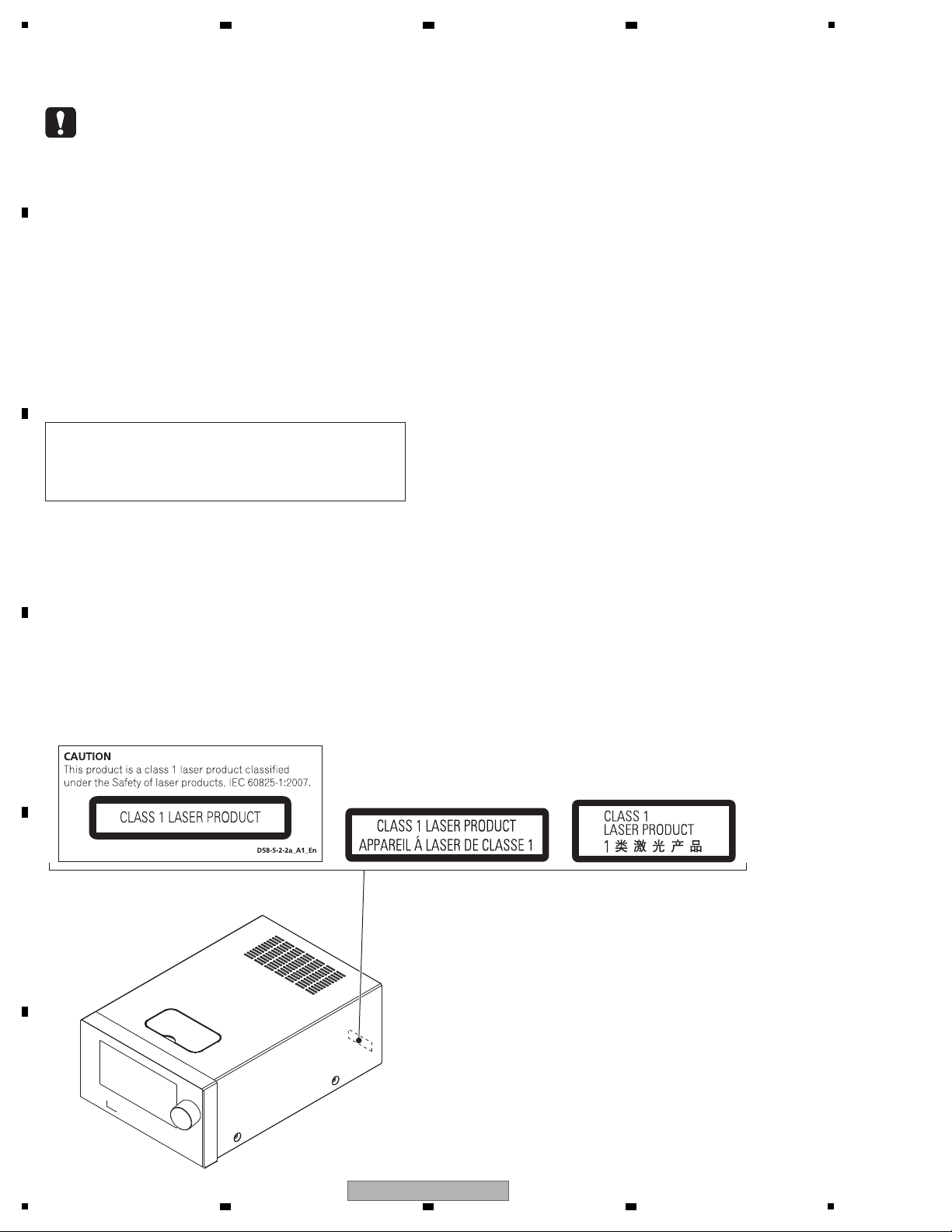
For CD Wave length (typ) : 790 nm
Operation output : 3 mW CW, Class 1
Maximum output : Class 1 (Under fault condition)
Laser Pickup specifications and Laser characteristics
LABEL CHECK
CXE model
SYXE8 model
AXQ5 model
2 3 4
SAFETY INFORMATION
A
B
C
D
E
F
2
1
2 3 4
X-HM81-K
Page 3

5
6 7 8
CONTENTS
SAFETY INFORMATION..........................................................................................................................................................2
1. SERVICE PRECAUTIONS....................................................................................................................................................4
1.1 NOTES ON SOLDERING........................................... ....................................................................................................4
1.2 WHEN REPLACING MECHA....................... ................................................ ... ...............................................................4
1.3 WHEN REPLACING CR870 (Module including BCO Assy)...........................................................................................4
2. SPECIFICATIONS.................................................................................................................................................................5
3. BASIC ITEMS FOR SERVICE..............................................................................................................................................6
3.1 CHECK POINTS AFTER SERVICING .............................................. .............................................................................6
3.2 JIGS LIST............................................. .......................................... ................................................................................6
3.3 PCB LOCATIONS...........................................................................................................................................................7
4. BLOCK DIAGRAM..............................................................................................................................................................10
4.1 OVERALL WIRING DIAGRAM.....................................................................................................................................10
4.2 OVERALL BLOCK DIAGRAM............................. ..........................................................................................................12
4.3 POWER SUPPLY BLOCK DIAGRAM...........................................................................................................................14
5. DIAGNOSIS........................................................................................................................................................................16
5.1 TROUBLESHOOTING..................................................................................................................................................16
5.2 PROTECTION CIRCUIT...............................................................................................................................................21
5.3 POWER MANAG EMENT....................................................... .......................................................................................24
5.4 CHECKING TERMINALS........................................... .......................................... ........................................................25
5.5 IC INFORMATION .................. .......................................... ............................................................................................28
6. SERVICE MODE.................................................................................................................................................................31
6.1 SERVICE MODE............................................. ... ..........................................................................................................31
6.2 PROTECT CHECK MODE ...........................................................................................................................................33
6.3 CHECKING THE LCD ............................. .......................................... ...........................................................................35
6.4 RDS CHARACTERS................................................... ..................................................................................................36
7. DISASSEMBLY ...................................................................................................................................................................37
8. EACH SETTING AND ADJUSTMENT................................................................................................................................45
8.1 UPDATING OF THE FIRMWARE.................................................................................................................................45
8.2 INITIAL SETTINGS......................................................................... ..............................................................................51
9. EXPLODED VIEWS AND PARTS LIST...............................................................................................................................52
.........
9.1 PACKING SECTION........................................... ...................................................................
9.2 EXTERIOR SECTION .................... ................................................................................. .............................................54
9.3 SPEAKER SECTION (S-HM81GB, S-HM81SA)..........................................................................................................58
9.4 SPAEKER SECTION (S-HM71)....................................................................................................................................59
10. SCHEMATIC DIAGRAM............................ ... ............................................... ... ...................................................................60
10.1 CD ASSY....................................................................................................................................................................60
10.2 TUNER and BT ASSYS..............................................................................................................................................62
10.3 MAIN ASSY (1/3)........................................................................................................................................................64
10.4 MAIN ASSY (2/3)........................................................................................................................................................66
10.5 MAIN ASSY (3/3)........................................................................................................................................................68
10.6 BCO ASSY (1/2).........................................................................................................................................................70
10.7 BCO ASSY (2/2).........................................................................................................................................................72
10.8 CNT1 ASSY................................................................................................................................................................74
10.9 CNT2 ASSY................................................................................................................................................................76
10.10 CNT3 ASSY ..............................................................................................................................................................78
10.11 F_AUX, F_USB, FRONT and KEY ASSYS ..............................................................................................................80
10.12 DOCKING ASSY ......................................................................................................................................................82
10.13 POWER ASSY..........................................................................................................................................................84
0.14 WAVEF
1
ORMS...........................................................................................................................................................86
11. PCB CONNECTION DIAGRAM........................ ................................................ ... .............................................................88
11.1 CD ASSY....................................................................................................................................................................88
11.2 TUNER and BT ASSYS..............................................................................................................................................90
11.3 MAIN ASSY................................................................................................................................................................92
11.4 BCO ASSY .................................................................................................................................................................96
11.5 CNT1, CNT2 and CNT3 ASSYS.................................................................................................................................98
11.6 F_AUX, F_USB, FRONT, KEY and DOCKING ASSYS............................................................................................102
11.7 POWER ASSY..........................................................................................................................................................106
12. PCB PARTS LIST..................... ... ................................................................................. ...................................................108
..............................52
A
B
C
D
E
F
X-HM81-K
5
6 7 8
3
Page 4
1
• For environmental protection, lead-free solder is used on the printed circuit boards mounted in this unit.
Be sure to use lead-free solder and a soldering iron that can meet specifications for use with lead-free solders for repairs
accompanied by reworking of soldering.
• Compared with conventional eutectic solders, lead-free solders have higher melting points, by approximately 40 ºC.
Therefore, for lead-free soldering, the tip temperature of a soldering iron must be set to around 373 ºC in general, although
the temperature depends on the heat capacity of the PC board on which reworking is required and the weight of the tip of
the soldering iron.
Do NOT use a soldering iron whose tip temperature cannot be controlled.
Compared with eutectic solders, lead-free solders have higher bond strengths but slower wetting times and higher melting
temperatures (hard to melt/easy to harden).
The following lead-free solders are available as service parts:
• Parts numbers of lead-free solder:
GYP1006 1.0 in dia.
GYP1007 0.6 in dia.
GYP1008 0.3 in dia.
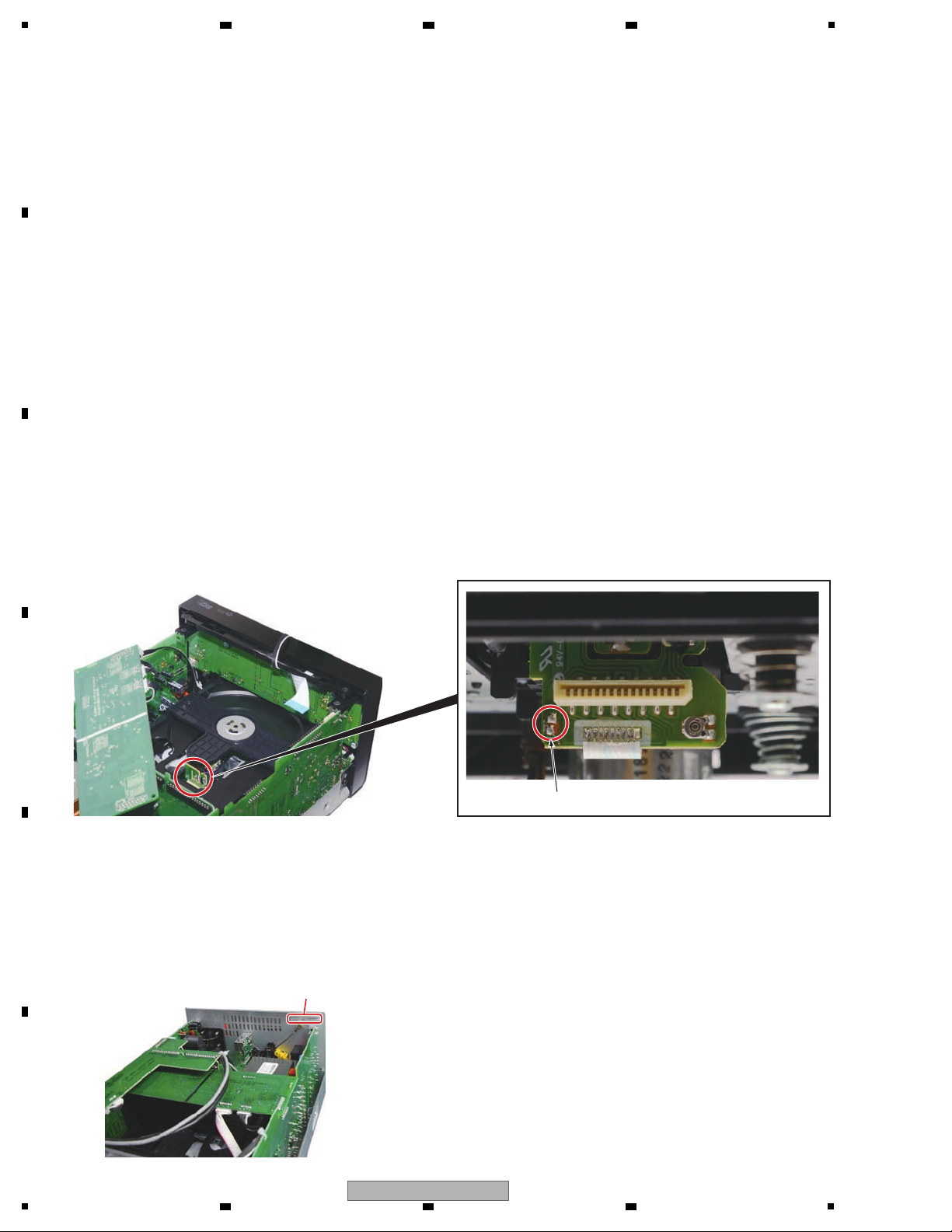
It is necessary to remove the soldering on the short circuit point after connecting the pickup flexible cable.
Short circuit point
After the CR870 module is replaced alone or the whole BCO Assy, including the CR870, is replaced, the MAC address will be
changed. Replace the MAC address seal with a new one, which you can find enclosed with the service part.
Attach the Mac Address label to the rear panel, above the WLAN antenna,
so that it will not block the ventilation holes on the rear panel.
MAC Address seal
2 3 4
1. SERVICE PRECAUTIONS
1.1 NOTES ON SOLDERING
A
B
C
1.2 WHEN REPLACING MECHA
D
1.3 WHEN REPLACING CR870 (Module including BCO Assy)
E
F
4
1
2 3 4
X-HM81-K
Page 5

5
Amplifier section
RMS Power Output ..................................................... 50 W + 50 W
(1 kHz, 10 % T.H.D., 4 ohms)
Guaranteed speaker impedance....................... 4 ohms to 16 ohms
Headphones.............................................. recommended: 32 ohms
Tuner section
Frequency Range (FM) ................................ 87.5 MHz to 108 MHz
Antenna Input (FM).........................................75 ohms unbalanced
Frequency Range (AM)..................................522 kHz to 1602 kHz
Antenna (AM) ............................................................Loop antenna
Video section
Signal level (Composite)...................................... 1 Vp-p (75 ohms)
Network section
LAN terminal................................................................Ethernet jack
10BASE-T/100BASE-TX
Other connectors
Power supply
USB connector...............................................................5 V, 2.1 A
iPod connector................................................................5 V, 1.0 A
ADAPTER Port (X-HM81 and XC-HM81 only) ...............5 V, 0.1 A
Miscellaneous
Power source............................................AC 220 V to 240 V, 50 Hz
Power consumption
Power on................................................................................75 W
Power standby.......................................................... 0.5 W or less
Network standby....................................................................17 W
Dimensions
Width ................................................................................215 mm
Height (X-HM71)..............................................................131 mm
Height (X-HM81 and XC-HM81)......................................32.2 mm
Depth................................................................................353 mm
Weight (X-HM71)................................................................... 5.0 kg
Weight (X-HM81 and XC-HM81)............................................5.5 kg
Speaker (X-HM81 only)
Type
2-way type speaker system
2.5 cm Dome-Tweeter
12 cm Woofer
Maximum input power..............................................................50 W
Impedance............................................................................ 4 ohms
Dimensions
Width ................................................................................156 mm
Height...............................................................................266 mm
Depth................................................................................258 mm
Weight ........................................................................... 4.3 kg/each
Speaker (X-HM71 only)
Type
2-way type speaker system
2 cm Dome-Tweeter
12 cm Woofer
Maximum input power..............................................................50 W
Impedance............................................................................ 4 ohms
Dimensions
Width ................................................................................148 mm
Height...............................................................................263 mm
Depth................................................................................208 mm
Weight ........................................................................... 2.7 kg/each
Note
• The specifications are applicable when the power supply is 230 V.
• Specifications and the design are subject to possible
modifications without notice, due to improvements.
• Corporation and product names mentioned herein are
trademarks or registered trademarks of the respective
corporations.
• This product is not designed for use in Japan.
• This product includes FontAvenue® fonts licensed by NEC
Corporation. FontAvenue® is a registered trademark of NEC
Corporation.
• Remote control
(SYXE8 model (AXD7676): 8300767600010-IL)
(CXE, AXQ5 model (AXD7680): 8300768000010-IL)
• AAA size IEC R03 dry cell batteries
(to confirm system operation) x 2
• AM loop antenna
(E601019000010-IL)
• FM wire antenna
(E605010140010-IL)
• WLAN antenna
(E600223170010-IL)
• Speaker x 2 (X-HM8
1 and X-HM71 only)
• Speaker wires x 2 (X-HM81 and X-HM71 only)
(X-HM81, X-HM71/AXQ5: 8952SHM810016-IL)
(X-HM71: 8952SHM700042-IL)
• Non skid pad x 8 (X-HM81 only)
(8952SHM810018-IL)
• Warranty card
• Quick Start Guide
(SYXE8 model: 5707000006940-IL)
(CXE model: 5707000006970-IL)
(AXQ5 model: 5707000006980-IL)
• Operating instructions (CD-ROM)
(6517000000821-IL)
Accessories
2. SPECIFICATIONS
6 7 8
A
B
C
D
5
X-HM81-K
6 7 8
E
F
5
Page 6
1
Item to be checked regarding audio
Distortion
Noise
Volume too low
Volume too high
Volume fluctuating
Sound interrupted
See the table below for the items to be checked regarding audio.
No. Check pointsProcedure
1
Confirm whether the customer complain has been solved.
The customer complain must not be reappeared.
Audio and operations must be normal.
6
Check the tuner operations.
Audio and operations (station search etc.) must be normal.
5
Check the Wi-fi antenna.
Confirm whether you refer to "5.4 CHECKING TERMINALS"
-"2. Checking the Wi-Fi Antenna", and the SSID of the wireless
LAN router is displayed.
7
Check the Line input playback. Audio and operations must be normal.
3
Check the USB playback.
Audio and operations must be normal.
4
Check the internet radio or Network audio playback.
Audio and operations must be normal.
2 Check the CD playback. Audio and operations (search etc.) must be normal.
Items to be checked after servicing
To keep the product quality after servicing, confirm recommended check points shown below.
8
Check the appearance of the product. No scratches or dirt on its appearance after receiving it
for service.
Jigs List
Jig Name Part No. Remarks
BtoB extension jig cable GGD1770 Diagnosis (POWER Assy ↔ CD Assy)
RS-232C update jig GGF1642 Firmware update
BtoB extension jig cable GGD1812 Diagnosis (MAIN Assy ↔ CD Assy)
BtoB extension jig cable GGD1811 Diagnosis (MAIN Assy ↔ CNT1 Assy)
FPC Extension jig GGD1813 Diagnosis (FRONT Assy ↔ CNT3 Assy)
Extension jig
FFC
GGD1774 Diagnosis (MECHA ↔ CD Assy)
3P Extension jig cable GGD1773 Diagnosis (MAIN Assy ↔ CNT2 Assy)
4P Extension jig cable GGD1809 Diagnosis (FRONT Assy ↔ CNT3 Assy)
Diagnosis (CNT2 Assy ↔ CNT3 Assy)BtoB extension jig cable GGD1810
Service remote control unit
GGF1381 Service mode
2 3 4
3. BASIC ITEMS FOR SERVICE
3.1 CHECK POINTS AFTER SERVICING
A
B
C
D
3.2 JIGS LIST
E
F
6
1
2 3 4
X-HM81-K
Page 7
L
KEY ASSY
BCO_STOPPER ASSY
M
DOCKING ASSY
J
F_USB ASSY
H
CNT3 ASSY
A
CD ASSY
D
MAIN ASSY
I
F_AUX ASSY
K
FRONT ASSY
F
CNT1 ASSY
N
POWER ASSY
G
CNT2 ASSY
E
BCO ASSY
B
TUNER ASSY
C
BT ASSY
(X-HM81 only)
MECHA
Cabinet (Bottom view)
5
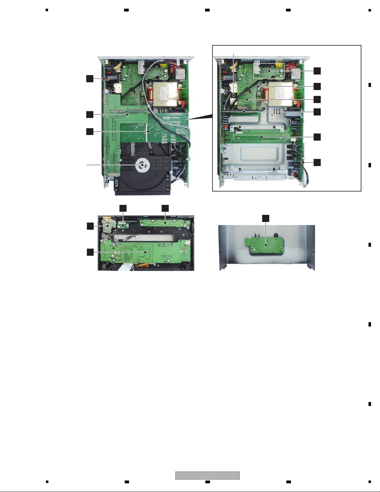
3.3 PCB LOCATIONS
6 7 8
A
B
C
D
E
F
X-HM81-K
5
6 7 8
7
Page 8
1
LIST OF ASSEMBLIES
NOTES: - Parts marked by “NSP” are generally unavailable because they are not in our Master Spare Parts List.
-
The > mark found on some component parts indicates the importance of the safety factor of the part.
Therefore, when replacing, be sure to use parts of identical designation.
Mark Symbol and Description
Mark Symbol and Description
X-HM81-K
/SYXE8
X-HM81-S
/SYXE8
XC-HM81-K
/SYXE8
XC-HM81-S
/SYXE8
X-HM71-K
/SYXE8
X-HM71-K
/CXE
X-HM71-S
/SYXE8
X-HM71-S
/AXQ5
NSP
NSP
1..PCB TOTAL ASSY FRONT 7025MU1105030-IL 7025MU1105030-IL 7025MU1105030-IL 7025MU1105030-IL
7025MU1106050-IL 7025MU1106020-IL 7025MU1106050-IL 7025MU1106020-IL
2..FRONT ASSY 7028072531010-IL 7028072531010-IL 7028072531010-IL 7028072531010-IL
7028072531010-IL 7028072531010-IL 7028072531010-IL 7028072531010-IL
2..KEY ASSY 7028072533010-IL 7028072533010-IL 7028072533010-IL 7028072533010-IL
2..CNT1 ASSY • • • • • • • • • • • • • • • • • • • •
NSP 2..CNT1 ASSY • • • • • • • • • • • • • • • • • • • •
NSP 2..CNT3 ASSY • • • • • • • • • • • • • • • • • • • •
NSP 2..CNT3 ASSY • • • • • • • • • • • • • • • • • • • •
NSP 2..BCO_STOPPER ASSY • • • • • • • • • • • • • • • • • • • •
NSP 2..BCO_STOPPER ASSY • • • • • • • • • • • • • • • • • • • •
7028072533010-IL 7028072533010-IL 7028072533010-IL 7028072533010-IL
2..TUNER ASSY 7028072534030-IL 7028072534030-IL 7028072534030-IL 7028072534030-IL
7028072534060-IL 7028072534040-IL 7028072534060-IL 7028072534040-IL
2..F_AUX ASSY 7028072535010-IL 7028072535010-IL 7028072535010-IL 7028072535010-IL
7028072535010-IL 7028072535010-IL 7028072535010-IL 7028072535010-IL
2..F_USB ASSY 7028072536010-IL 7028072536010-IL 7028072536010-IL 7028072536010-IL
7028072536010-IL 7028072536010-IL 7028072536010-IL 7028072536010-IL
2..BT ASSY 7028072537010-IL 7028072537010-IL 7028072537010-IL 7028072537010-IL
Not used Not used Not used Not used
NSP 1..PCB TOTAL ASSY POWER 7025MU1105031-IL 7025MU1105031-IL 7025MU1105031-IL 7025MU1105031-IL
7025MU1106051-IL 7025MU1106021-IL 7025MU1106051-IL 7025MU1106031-IL
2..MAIN ASSY 7028072541030-IL 7028072541030-IL 7028072541030-IL 7028072541030-IL
7028072541060-IL 7028072541040-IL 7028072541060-IL 7028072541050-IL
2..POWER ASSY 7028072542030-IL 7028072542030-IL 7028072542030-IL 7028072542030-IL
7028072542030-IL 7028072542040-IL 7028072542030-IL 7028072542030-IL
2..DOCKING ASSY 7028072544010-IL 7028072544010-IL 7028072544010-IL 7028072544010-IL
7028072544010-IL 7028072544010-IL 7028072544010-IL 7028072544010-IL
NSP 1..PCB TOTAL ASSY BRIDG 7025MU1105032-IL 7025MU1105032-IL 7025MU1105032-IL 7025MU1105032-IL
7025MU1106022-IL 7025MU1106022-IL 7025MU1106022-IL 7025MU1106022-IL
2..BCO ASSY 7028072551010-IL 7028072551010-IL 7028072551010-IL 7028072551010-IL
7028072551020-IL 7028072551020-IL 7028072551020-IL 7028072551020-IL
2..CNT2 ASSY 7028072552010-IL 7028072552010-IL 7028072552010-IL 7028072552010-IL
7028072552020-IL 7028072552020-IL 7028072552020-IL 7028072552020-IL
1...PCB TOTAL ASSY CD 7025MU1105034-IL 7025MU1105034-IL 7025MU1105034-IL 7025MU1105034-IL
7025MU1105034-IL 7025MU1105034-IL 7025MU1105034-IL 7025MU1105034-IL
2..CD ASSY 7028072301010-IL 7028072301010-IL 7028072301010-IL 7028072301010-IL
7028072301010-IL 7028072301010-IL 7028072301010-IL 7028072301010-IL
MECHA
NSP 1..PCB TOTAL ASSY FRONT
2..FRONT ASSY
2..KEY ASSY
2..TUNER ASSY
2..F_AUX ASSY
2..F_USB ASSY
2..BT ASSY
NSP 1..PCB TOTAL ASSY POWER
2..MAIN ASSY
2..POWER ASSY
2..DOCKING ASSY
NSP 1..PCB TOTAL ASSY BRIDG
2..BCO ASSY
2..CNT2 ASSY
1...PCB TOTAL ASSY CD
2..CD ASSY
MECHA
8030000010080-IL 8030000010080-IL 8030000010080-IL 8030000010080-IL
8030000010080-IL 8030000010080-IL 8030000010080-IL 8030000010080-IL
A
2 3 4
B
C
D
E
F
8
1
X-HM81-K
2 3 4
Page 9

5
6 7 8
A
B
C
D
E
F
X-HM81-K
5
6 7 8
9
Page 10
1
I
F_AUX ASSY
(7028072535010-IL)
J
F_USB ASSY
(7028072536010-IL)
K
FRONT ASSY
(7028072531010-IL)
LCD
H
CNT3 ASSY
CP30 CP31
CP607
CN510
CP19
CP18
FPC2
CP606
CP512
CP509
CP602
CP712
CP605
CP400
CN702
CP8
PN1702
1: A_+12V
2: A_+12V
3: A_GND
4: A_GND
5: A_-12V
6: A_-12V
7: A_GND
8: CD_L
9: A_GND
10: CD_R
11: M_GND
12: M_GND
13: CD_RX
14: CD_TX
15: CD_RST
16: MAIN_BUSY
17: NC
1: VFD_CE
2: VFD_CLK
3: VFD_DI
1: B+_27V
2: B+_27V
3: AMP_GND
4: AMP_GND
5: LCH_AMP_GND
6: LCH_AMP_GND
7: RCH_AMP_GND
8: RCH_AMP_GND
9: B-_27V
10: B-_27V
11: RLY_GND
12: RLY_GND
13: AMP_-5V
14: AMP_-5V
15: POWER_PROT
16: AMP_+5V
17: PD
18: STBY_RLY
19: M_GND
20: M_GND
21: MICOM_3V9
22: MICOM_3V9
23: DGND
24: DGND
25: NC
26: NC
1: SW_GND
2: SW_OUT
3: A_GND
4: BT/TU_R
5: A_GND
6: BT/TU_L
7: A_GND
8: USB_R
9: A_GND
10: USB_L
11: A_GND
12: LINE_IN_R
13: A_GND
14: LINE_IN_L
15: A_GND
16: A_GND
17: A_GND
18: +12V
19: +12V
1: SW_GND
2: SW_OUT
3: A_GND
4: BT/TU_R
5: A_GND
6: BT/TU_L
7: A_GND
8: USB_R
9: A_GND
10: USB_L
11: A_GND
12: LINE_IN_R
13: A_GND
14: LINE_IN_L
15: A_GND
16: A_GND
17: A_GND
18: +12V
19: +12V
1: +12V
2: +12V
3: A_GND
4: A_GND
5: -12V
6: -12V
7: A_GND
8: CD_L
9: A_GND
10: CD_R
11: M_GND
12: M_GND
13: CD_RX
14: CD_TX
15: CD_RST
16: MAIN_BUSY
17: NC
1: LCDGND
2: LCDGND
3: IOVCC(+3.3V)
4: IOVCC(+3.3V)
1: HP_R
2: H/P_GND
3: HP_L
4: H/P_GND
5: FAUX_R
6: AUX_GND
7: FAUX_L
8: HP_DET
1: GND
2: GND
3: IOVCC(+3.3V)
4: IOVCC(+3.3V)
1: CPU_GND
2: KEY2
1: GND
2: VCI(+3.3V)
3: RESX
4: DB0/B0
5: DB1/B1
6: DB2/B2
7: DB3/B3
8: DB4/B4
9: DB5/B5
10: DB6/G0
11: DB7/G1
12: DB8/G2
13: DB9/G3
14: DB10/G4
15: DB11/G5
16: DB12/R0
17: DB13/R1
18: DB14/R2
19: DB15/R3
20: DB16/R4
21: DB17/R5
22: CSX
23: SCL
24: DE
25: DOTCLK
26: HSYNC
27: VSYNC
28: SDA
29: LED-A+
30: LED-K1
31: LED-K2
32: LED-K3
33: LED-K4
34: IOVCC(+3.3V)
35: GND
1: USB_VCC
2: USB_VCC
3: USBHO_D-
4: USBHO_D+
5: USB_GND
6: USB_GND
7: NC
1: DAC_RST
2: AUDIO_SEL
3: SUB_PDN
4: SUB_IRQ
5: SUB_ON
6: SUB_RESET
7: MAIN_IRQ
8: SCDI_MAIN
9: SCDO_MAIN
10: CSCK_MAIN
11: I_POD_DET
12: GPIO2_DAB_RX
13: SDIO_DAB_TX
14: TU_SCLK
15: TU_SEN
16: TU/DAB_RST
17: SW_MUTEBASE
18: VIDEO_MUTE
19: IPOD_CHARGE_LED
20: POWER_ON_LED
21: KEY2
22: KEY1
23: REMOTE
24: TIMER_LED
25: VOLUME+
26: VOLUME27: M3V3
28: M3V3_SW
29: CPU_GND
30: CPU_GND
31: CPU_GND
1: HP_R
2: H/P_GND
3: HP_L
4: H/P_GND
5: FAUX_R
6: AUX_GND
7: FAUX_L
8: HP/DET
1: VIDEO_GND
2: VIDEO_GND
3: DOCK_CVBS
4: SW_GND
5: SW_OUT
6: A_GND
7: LINE_IN_R
8: A_GND
9: LINE_IN_L
10: A_GND
11: DAB/TU_R
12: A_GND
13: DAB/TU_L
14: A_GND
15: VIDEO_MUTE
16: SW_MUTEBASE
17: TU/DAB_RST
18: TU_SEN
19: TU_SCLK
20: GPIO2 DAB_RX
21: SDIO DAB_TX
22: A_GND
23: A_GND
24: TU_+5V
25: TU_+5V
CP31
1: USB_R
2: A_GND
3: USB_L
4: +12V
5: +12V
6: DAC_RESET
7: AUDIO_SEL
8: SW_GND
9: SW_OUT
10: A_GND
11: LINE_IN_R
12: A_GND
13: LINE_IN_L
14: A_GND
15: BT/TU_R
16: A_GND
17: BT/TU_L
18: A_GND
19: VIDEO_MUTE
20: SW_MUTEBASE
21: TU_RST(DAB_RST)
22: TU_SEN
23: TU_SCLK
24: SDIO DAB_RX
25: GPIO2 DAB_TX
26: I_POD_DET
27: CSCK_MAIN
28: SCDO_MAIN
29: SCDI_MAIN
30: MAIN_IRQ
31: SUB_RESET
32: SUB_ON
33: SUB_IRQ
CP30
1: RESX
2: DB0/B0
3: DB1/B1
4: DB2/B2
5: DB3/B3
6: DB4/B4
7: DB5/B5
8: DB6/G0
9: DB7/G1
10: DB8/G2
11: DB9/G3
12: DB10/G4
13: DB11/G5
14: DB12/R0
15: DB13/R1
16: DB14/R2
17: DB15/R3
18: DB16/R4
19: DB17/R5
20: SCL
21: DE
22: CSX
23: DOTCLK
24: HSYNC
25: VSYNC
26: SDA
27: LED-A+
28: LED-CTL
29: IOVCC(+3.3V)
30: IOVCC(+3.3V)
31: GND
32: GND
33: SUB_PDN
FPC2
1: CPU_GND
2: M3V3_SW
3: M3V3
4: KEY2
5: KEY1
6: CPU_GND
7: REMOTE
8: TIMER_LED
9: VOLUME+
10: VOLUME11: RESX
12: DB0/B0
13: DB1/B1
14: DB2/B2
15: DB3/B3
16: DB4/B4
17: DB5/B5
18: DB6/G0
19: DB7/G1
20: DB8/G2
21: DB9/G3
22: DB10/G4
23: DB11/G5
24: DB12/R0
25: DB13/R1
26: DB14/R2
27: DB15/R3
28: DB16/R4
29: DB17/R5
30: CSX
31: SCL
32: DE
33: DOTCLK
34: HSYNC
35: VSYNC
36: SDA
37: LED-A+
38: LED-CTL
39: LED_B
40: LED_A
1: CPU_GND
2: M3V3_SW
3: M3V3
4: KEY2
5: KEY1
6: CPU_GND
7: REMOTE
8: TIMER_LED
9: VOLUME+
10: VOLUME-
11: RESX
12: DB0/B0
13: DB1/B1
14: DB2/B2
15: DB3/B3
16: DB4/B4
17: DB5/B5
18: DB6/G0
19: DB7/G1
20: DB8/G2
21: DB9/G3
22: DB10/G4
23: DB11/G5
24: DB12/R0
25: DB13/R1
26: DB14/R2
27: DB15/R3
28: DB16/R4
29: DB17/R5
30: CSX
31: SCL
32: DE
33: DOTCLK
34: HSYNC
35: VSYNC
36: SDA
37: LED-A+
38: LED-CTL
39: LED_B
40: LED_A
1: BT
2: AG
3: BT
4: GN
5: SU
6: SU
7: SU
8: MA
9: CS
10: S
11: S
12: M
13: IP
14:
M
15: V
16: D
17: D
18: D
19: D
20: V
21: V
22: V
23: A
24: A
25: A
CP11
1: RESX
2: DB0/B0
3: DB1/B1
4: DB2/B2
5: DB3/B3
6: DB4/B4
7: DB5/B5
8: DB6/G0
9: DB7/G1
10: DB8/G2
11: DB9/G3
12: DB10/G4
13: DB11/G5
14: DB12/R0
15: DB13/R1
16: DB14/R2
17: DB15/R3
18: DB16/R4
19: DB17/R5
20: CSX
21: SCL
22: DE
23: DOTCLK(GND_S
24: HSYNC
25: VSYNC
26: SDA
27: LED-A+
28: LED-CTL(SPSW
29: IOVCC(+3.3V)
30: IOVCC(+3.3V)
31: GND
32: GND
33: GND
CP12
1: BT_R
2: AGND
3: BT_L
4: AGND
5: SUB_IRQ
6: SUB_RESET
7: SUB_PDN
8: MAIN_SUB_IPOD_DET
9: CSK_MAIN
10: SCDO_MAIN
11: SCDI_MAIN
12: MAIN_IRQ
13: DOCKING_CVBS
14: MAIN_USB_POWER
15: VGND
16: DM-870-SCLK
17: DM-870-MCLK
18: DM-870-LRCK
19: DM-870-DATA
20: VFD_DI
21: VFD_CLK
22: VFD_CE
23: AMP-5V
24: AMP+5V
25: NC
CN515
CP500
CP508
FPC515
MOD500
CP604
-
When ordering service parts, be sure to refer to "EXPLODED VIEWS and PARTS LIST" or "PCB PARTS LIST".
-
The > mark found on some component parts indicates the importance of the safety factor of the part.
Therefore, when replacing, be sure to use parts of identical designation.
-
: The power supply is shown with the marked box.
B
(7028072534030-IL: X-HM81, XC-HM81)
(7028072534060-IL: X-HM71/SYXE8)
(7028072534040-IL: X-HM71/CXE, AXQ5)
D
MAIN ASSY
(7028072541030-IL: X-HM81, XC-HM81)
(7028072541060-IL: X-HM71/SYXE8)
(7028072541040-IL: X-HM71/CXE)
(7028072541050-IL: X-HM71/AXQ5)
D
1/3-D3/3
TUNER ASSY
1: B+_27V
2: B+_27V
3: AMP_GND
4: AMP_GND
5: AMP_GND_L
6: AMP_GND_L
7: AMP_GND_R
8: AMP_GND_R
9: B-_27V
10: B-_27V
11: SPKRLY_GND
12: SPKRLY_GND
13: AMP_-5V
14: AMP_-5V
15: AMP_+5V
16: POWER_PROT
17: P/D
18: STBY_RLY
19: M_GND
20: M_GND
21: MICOM_3V9
22: MICOM_3V9
23: DGND
24: DGND
25: NC
26: NC
CP18
1: DAC_RST
2: AUDIO_SEL
3: SUB_PDN
4: SUB_IRQ
5: SUB_ON
6: SUB_RESET
7: MAIN_IRQ
8: SCDI_MAIN
9: SCDO_MAIN
10: CSCK_MAIN
11: I_POD_DET
12: GPIO2_DAB_RX
13: SDIO_DAB_TX
14: TU_SCLK
15: TU_SEN
16: TU/DAB_RST
17: SW_MUTEBASE
18: VIDEO_MUTE
19: IPOD_CHARGE_LED
20: POWER_ON_LED
21: KEY2
22: KEY1
23: REMOTE
24: TIMER_LED
25: VOLUME+
26: VOLUME27: M3V3
28: M3V3_SW
29: CPU_GND
30: CPU_GND
31: CPU_GND
2 3 4
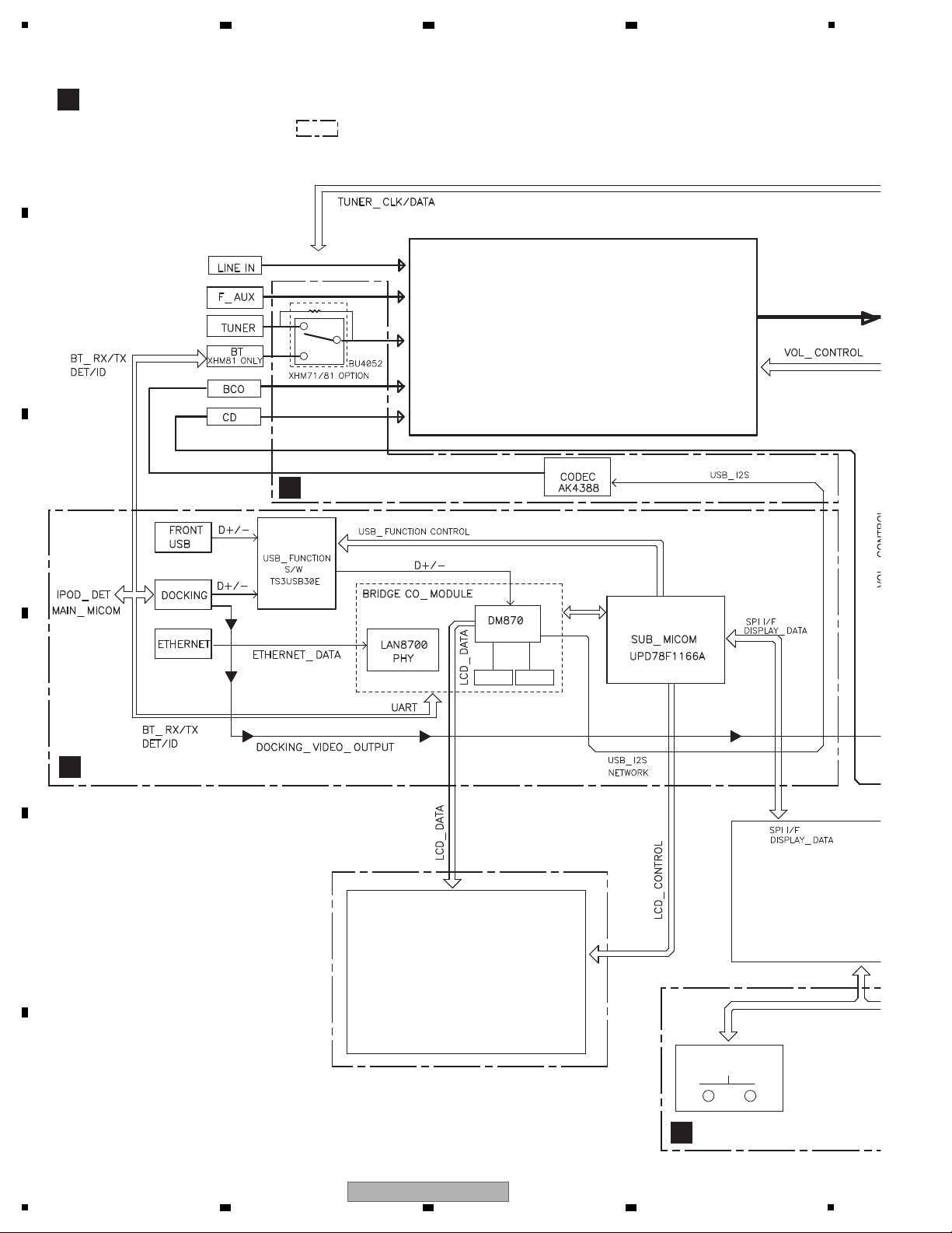
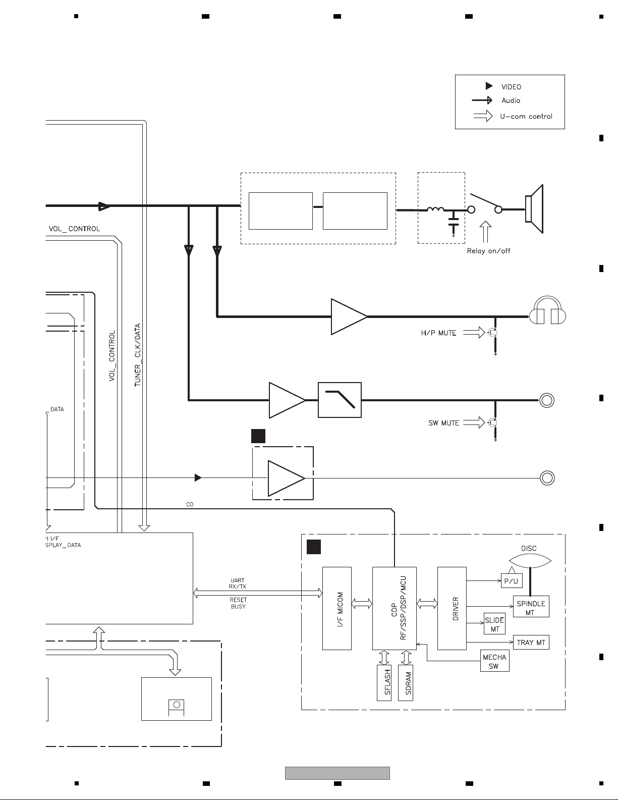
4. BLOCK DIAGRAM
4.1 OVERALL WIRING DIAGRAM
A
B
C
D
E
F
10
1
X-HM81-K
2 3 4
Page 11
C
BT ASSY
(7028072537010-IL)
MECHA
(8030000010080-IL)
M
DOCKING ASSY
(7028072544010-IL)
A
CD ASSY
(7028072301010-IL)
F
CNT1 ASSY
L
KEY ASSY
(7028072533010-IL)
PN1603
PN1602
PN1705
CP310
CP312
CP710
CP402
CP402
CN511
CP1001
CP6
CP2
CP4
CP1
CP5
CN702
CP8
CP8
CP7
CP7
CP12
CP505 CP506
CP11
CP301
AC IN
PN1702
1: A_+12V
2: A_+12V
3: A_GND
4: A_GND
5: A_-12V
6: A_-12V
7: A_GND
8: CD_L
9: A_GND
10: CD_R
11: M_GND
12: M_GND
13: CD_RX
14: CD_TX
15: CD_RST
16: MAIN_BUSY
17: NC
1: MOTRO_GND
2: MOTRO_GND
3: MOTRO_+8V
4: MOTRO_+8V
5: CD_GND
6: CD_GND
7: CD_3V3
8: CD_3V3
9: NC
10: A_+12V
11: A_+12V
12: A_GND
13: A_GND
14: A_-12V
15: A_-12V
1: MOT_GND
2: MOT_GND
3: MOT_+8V
4: MOT_+8V
5: CD3.3V_GND
6: CD3.3V_GND
7: CD_3.3V
8: CD_3.3V
9: NC
10: A_+12V
11: A_+12V
12: A_GND
13: A_GND
14: A_-12V
15: A_-12V
1: CPU_GND
2: KEY2
1: CPU_GND
2: KEY2
1: VIDEO_GND
2: VIDEO_GND
3: DOCK_CVBS
4: SW_GND
5: SW_OUT
6: A_GND
7: LINE_IN_R
8: A_GND
9: LINE_IN_L
10: A_GND
11: DAB/TU_R
12: A_GND
13: DAB/TU_L
14: A_GND
15: VIDEO_MUTE
16: SW_MUTEBASE
17: TU/DAB_RST
18: TU_SEN
19: TU_SCLK
20: DAB_RX GPIO2
21: DAB_TX SDIO
22: A_GND
23: A_GND
24: TU_+5V
25: TU_+5V
CP505
1: USB_R
2: A_GND
3: USB_L
4: +12V
5: +12V
6: DAC_RESET
7: AUDIO_SEL
8: SW_GND
9: SW_OUT
10: A_GND
11: LINE_IN_R
12: A_GND
13: LINE_IN_L
14: A_GND
15: BT/TU_R
16: A_GND
17: BT/TU_L
18: A_GND
19: VIDEO_MUTE
20: SW_MUTEBASE
21: TU_RST(DAB_RST)
22: TU_SEN
23: TU_SCLK
24: SDIO DAB_RX
25: GPIO2 DAB_TX
26: I_POD_DET
27: CSCK_MAIN
28: SCDO_MAIN
29: SCDI_MAIN
30: MAIN_IRQ
31: SUB_RESET
32: SUB_ON
33: SUB_IRQ
CP506
1: RESX
2: DB0/B0
3: DB1/B1
4: DB2/B2
5: DB3/B3
6: DB4/B4
7: DB5/B5
8: DB6/G0
9: DB7/G1
10: DB8/G2
11: DB9/G3
12: DB10/G4
13: DB11/G5
14: DB12/R0
15: DB13/R1
16: DB14/R2
17: DB15/R3
18: DB16/R4
19: DB17/R5
20: SCL
21: DE
22: CSX
23: DOTCLK
24: HSYNC
25: VSYNC
26: SDA
27: LED-A+
28: LED-CTL
29: IOVCC(+3.3V)
30: IOVCC(+3.3V)
31: GND
32: GND
33: SUB_PDN
1: BT_R
2: AGND
3: BT_L
4: GND
5: SUB_IRQ
6: SUB_RESET
7: SUB_PDN
8: MAIN_IPOD_DET
9: CSK_MAIN
10: SCDO_MAIN
11: SCDI_MAIN
12: MAIN_IRQ
13: IPOD_CVBS
14:
MAIN_USB_POWER (NC)
15: VGND
16: DM-870-SCLK
17: DM-870-MCLK
18: DM-870-LRCK
19: DM-870-DATA
20: VFD_DI
21: VFD_CLK
22: VFD_CE
23: AMP-5V
24: AMP+5V
25: AMP+5V
1: GND
2: GND
3: GND
4: IOVCC(+3.3V)
5: IOVCC(+3.3V)
6: LED-CTL(SPSW)
7: LED-A+
8: SDA
9: VSYNC
10: HSYNC
11: DOTCLK
12: DE
13: CLK
14: CSX
15: DB17/R5
16: DB16/R4
17: DB15/R3
18: DB14/R2
19: DB13/R1
20: DB12/R0
21: DB11/G5
22: DB10/G4
23: DB9/G3
24: DB8/G2
25: DB7/G1
26: DB6/G0
27: DB5/B5
28: DB4/B4
29: DB3/B3
30: DB2/B2
31: DB1/B1
32: DB0/B0
33: RESX
CP11
1: RESX
2: DB0/B0
3: DB1/B1
4: DB2/B2
5: DB3/B3
6: DB4/B4
7: DB5/B5
8: DB6/G0
9: DB7/G1
10: DB8/G2
11: DB9/G3
12: DB10/G4
13: DB11/G5
14: DB12/R0
15: DB13/R1
16: DB14/R2
17: DB15/R3
18: DB16/R4
19: DB17/R5
20: CSX
21: SCL
22: DE
23: DOTCLK(GND_SHIELD)
24: HSYNC
25: VSYNC
26: SDA
27: LED-A+
28: LED-CTL(SPSW)
29: IOVCC(+3.3V)
30: IOVCC(+3.3V)
31: GND
32: GND
33: GND
1: GND
2: GND
3: GND
4: VDD
5: VDD
6: VDD
7: +5V
8: -5V
1: VFD_DI
2: VFD_CLK
3: VFD_CE
1: -5V
2: +5V
3: BCO_+12V
4: BCO_+12V
5: BCO_+12V
6: BCO_GND
7: BCO_GND
8: BCO_GND
1: D-
2: D+
3: +5V
4: GND
5: GND
6: IPOD_DET
7: IPOD_CVBS
8: MIITXCLK
1: ACCESSORY_PWR
2: C_VID
3: IPOD_DET
4: D_GND
5: D_GND
6: USB_+5V
7: USB_D+
8: USB_D-
1: +5V
2: +5V
3: D-
4: D+
5: GND
6: GND
1: BT_MUTE
2: BT_R
3: AGND
4: BT_L
5: BCO_GND
6: BT_ON/CE
7: BT_+5V
8: BT_ID
9: BT_DET
10: BT_TX/U_RX
11: BT_RX/U_TX
12: BT_/OC
1: BT_MUTE
2: BT_R
3: A_GND
4: BT_L
5: BCO_GND
6: BT_ON/CE
7: BT_+5V
8: BT_ID
9: BT_DET
10: BT_TX/U_RX
11: BT_RX/U_TX
12: BT_/OC
1: SP+
2: SP-
3: SL+
4: SL-
5: Limit SW
6: GND
1: CLOSE_SW
2: GND
3: OPEN_SW
4: MOTOR_+
5: MOTOR_-
1: F-
2: T+
3: T-
4: F+
5: PD
6: VR
7: LD
8: GND
9: F
10: C
11: B
12: A
13: D
14: E
15: SVCC
16: VREF
CP508
CN502
PN1604
X-HM81,
XC-HM81
ONLY
(7028072551010-IL: X-HM81, XC-HM81)
(7028072551020-IL: X-HM71)
BCO ASSY
E
E
1/2-E2/2
N
POWER ASSY
(7028072542030-IL:
X-HM81,XC-HM81)
(7028072542030-IL:
X-HM71/SYXE8, AXQ5)
(7028072542040-IL:
X-HM71/CXE)
G
CNT2 ASSY
(7028072552010-IL: X-HM81, XC-HM81)
(7028072552020-IL: X-HM71)
1: B+_27V
2: B+_27V
3: AMP_GND
4: AMP_GND
5: AMP_GND_L
6: AMP_GND_L
7: AMP_GND_R
8: AMP_GND_R
9: B-_27V
10: B-_27V
11: SPKRLY_GND
12: SPKRLY_GND
13: AMP_-5V
14: AMP_-5V
15: AMP_+5V
16: POWER_PROT
17: P/D
18: STBY_RLY
19: M_GND
20: M_GND
21: MICOM_3V9
22: MICOM_3V9
23: DGND
24: DGND
25: NC
26: NC
1: MICOM_3V9
2: MICOM_3V9
3: M_GND
4: M_GND
5: STBY_RLY
6: P/D
7: NC
8: POWER_PROT
9: AMP_+5V
10: AMP_+5V
11: AMP_-5V
12: AMP_-5V
13: SPKRLY_GND
14: SPKRLY_GND
15: B-_27V
16: B-_27V
17: AMP_GND_R
18: AMP_GND_R
19: AMP_GND_L
20: AMP_GND_L
21: AMP_GND
22: AMP_GND
23: B+_27V
24: B+_27V
25: BCO_GND
26: BCO_GND
27: BCO_GND
28: BCO_+12V
29: BCO_+12V
30: BCO_+12V
1: MICOM_3V9
2: MICOM_3V9
3: M_GND
4: M_GND
5: STBY_RLY
6: P/D
7: NC
8: POWER_PROT
9: AMP_+5V
10: AMP_+5V
11: AMP_-5V
12: AMP_-5V
13: SPKRLY_GND
14: SPKRLY_GND
15: B-_27V
16: B-_27V
17: AMP_GND
18: AMP_GND
19: AMP_GND
20: AMP_GND
21: AMP_GND
22: AMP_GND
23: B+_27V
24: B+_27V
25: BCO_GND
26: BCO_GND
27: BCO_GND
28: BCO_+12V
29: BCO_+12V
30: BCO_+12V
5
6 7 8
A
B
C
D
5
X-HM81-K
6 7 8
E
F
11
Page 12
1
NAND_Flash
SDRAM
LCD
KEY
IC4
IC609
IC603
CR870
IC12, 18, 19
IC208
IC704
SYSTEM U
M3030
NJU7391
INPUT SELECT & VOLUME
K
FRONT ASSY
E
BCO ASSY
D
MAIN ASSY
G
CNT2 ASSY
LCD
Note: Be blocks in MAIN ASSY other than blocks.
(There are some exceptions)
2 3 4
4.2 OVERALL BLOCK DIAGRAM
A
B
C
D
E
F
12
1
2 3 4
X-HM81-K
Page 13
5
-6dB
AMP
CVBS
OUT
IR
MOSFET
AMP BLOCK
CD BLOCK
IC1602
IC1603
IC1606
IC1604
IC609
IC608, 612
IC1601
IC605
Q610,615,619,621
IC606
IC400
RMC500
Headphone
OUT
+6dB
IRF6645
IRS2092S
Subwoofer
OUT
Speaker
OUT
DOCKING_VIDEO
LC_FILTER
SYSTEM U-com
M30302
B
TUNER ASSY
A
CD ASSY
6 7 8
A
B
C
D
X-HM81-K
5
6 7 8
E
F
13
Page 14
1
MAIN TRANS
AC CORD
B+_27V
BCO_+12V
MOT_+8V
MICOM_
B-_27V
IC301
IC303
IC311
IC315
S2(+12V,-12V)
SUB TRANS
S3(USB/CD)
S1(AMP +B)
2 3 4
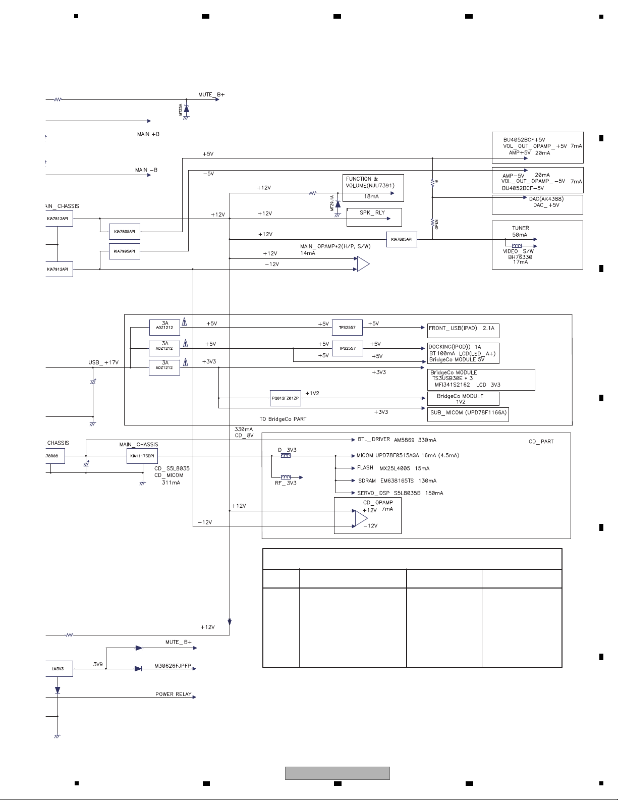
4.3 POWER SUPPLY BLOCK DIAGRAM
A
B
C
D
E
F
14
1
2 3 4
X-HM81-K
Page 15
5
S1
S2
21.5V
13.6V
0.46A
2.2A
33V
S3
8.7V
4.2A
-33V(NO LOAD)
+33V(NO LOAD)
B+_27V
A_+12V
AMP_+5V
AMP_-5V
A_-12V
BCO_+12V
MOT_+8V
MICOM_3V9
CD_+3.3V
B-_27V
IC301
IC303
IC701
IC11
IC14
IC2
IC9
IC5
IC313
IC315
IC13
IC305
IC307
20.2V
RATED_VOLTAGE
NO_LOAD
17.4V
MAIN TRANS SPEC(-)
CURRENT
6 7 8
A
B
C
D
E
F
X-HM81-K
5
6 7 8
15
Page 16
1
• No Power
• Detection DC from AMP circuit.
Check the IC608, IC612 and its peripheral circuits. (MAIN Assy)
• Detection overvoltage on +B line.
Check the D307 and its peripheral circuits. (POWER Assy)
Yes
• Detection abnormality of the AMP circuit.
Check the IC608, IC612 and its peripheral circuits. (MAIN Assy)
Yes
• Detection abnormal temperature of the AMP L ch circuit.
Check the IC608 and its peripheral circuits. (MAIN Assy)
Yes
• Detection short-circuit on power supply circuits.
D307: B+_27V, B-_27V
IC305, IC307: AMP_+5V, AMP_-5V
IC315: MICOM_3V9
IC301, IC303: A_+12V, A_-12V
IC313: CD_3.3V
Check each IC mentioned above and peripheral circuits.
• Check workings of primary relay (RLY301).
• Check whether secondary fuse (FU302 to 305) does not perform blowout.
(POWER Assy)
Yes
No
Protect (protection history)
Does DC protect work?
No
No
No
Does POWER protect
work?
Does AMP protect
work?
• Detection PWM abnormality output of the AMP circuit.
Check the IC608, IC612 and its peripheral circuits. (MAIN Assy)
Yes
Does PWM protect
work?
No
X-HM81, XC-HM81 only
No
• Detection an overcurrent of Bluetooth power
Check the IC600 and its peripheral circuits.
Check the short-circuit of BT_+5V power (BT Assy).
Yes
Yes
Does BT Protect
work?
No
• Detection an overcurrent of power of Front USB or iPod Dock.
Check the IC11 and IC14 and its peripheral circuits.
Check the short-circuit of 5V power of Front USB or iPod Dock
(BCO Assy/DOCKING Assy/F_USB Assy).
Be not the trouble that each Protect circuit works.
Does USB protect
work?
Does
OVERTEMP1 protect
work?
• Detection abnormal temperature of the AMP R ch circuit.
Check the IC612 and its peripheral circuits. (MAIN Assy)
Yes
No
Does
OVERTEMP2 protect
work?
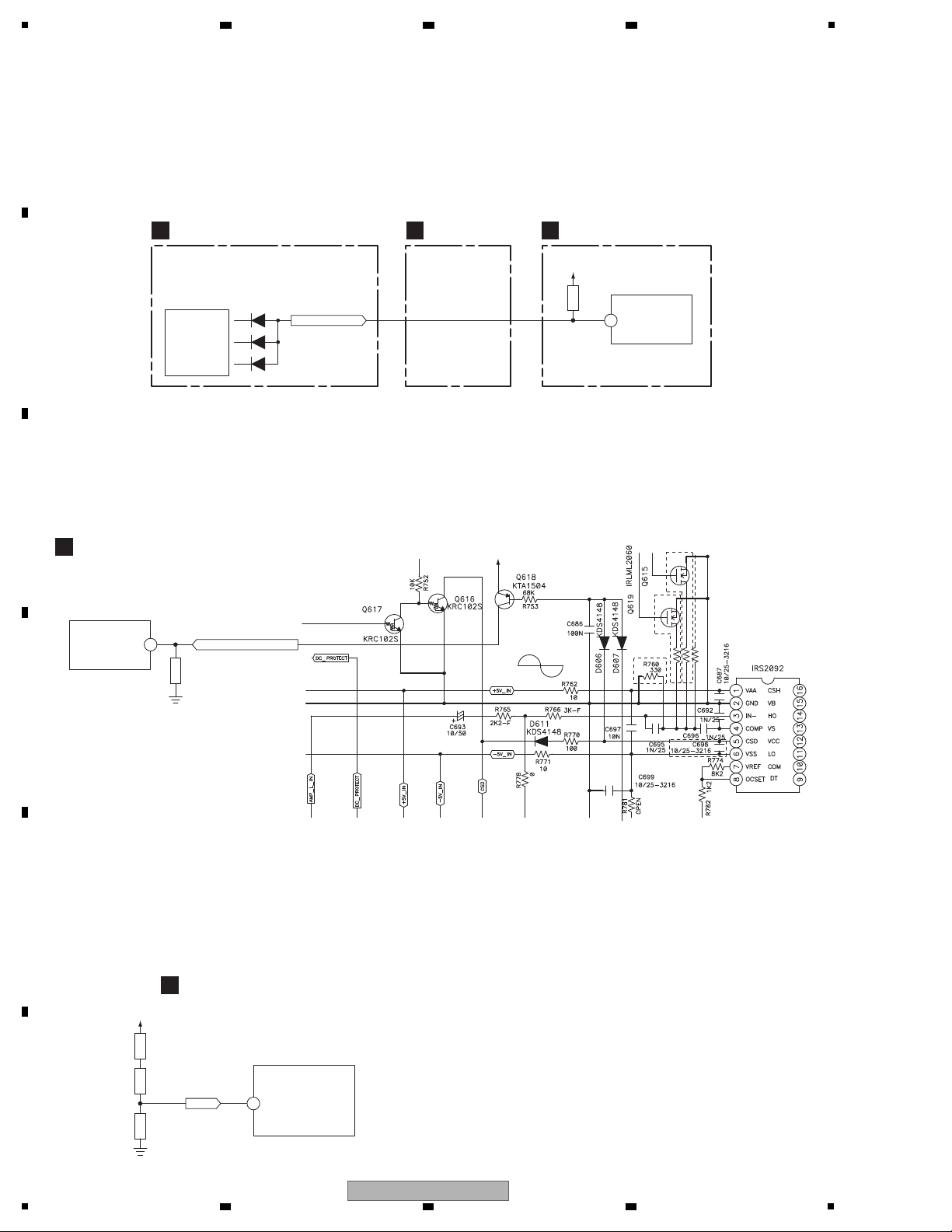
5. DIAGNOSIS
5.1 TROUBLESHOOTING
A
2 3 4
B
C
D
E
F
16
1
X-HM81-K
2 3 4
Page 17
• No Sound
(*1) The confirmation that is in a state of each sound source
Check the state of each sound source. (*1)
Yes
No
A sound does not come out
of FRONT SP
The sound from a source of CD,
USB, TUNER, iPod, LINE, F.AUX
does not come out.
• Check the IC602 and its peripheral circuits. (MAIN Assy)
• Check the MAIN MUTE circuit.
No
[Failure in the individual analog-signal paths]
• Check each input circuit part and each Assy.
• Failure in connection for volume IC (IC603).
• Check the IC603 and its peripheral circuits.
No
Yes -> Check the BCO system audio.
(USB/iPod/Ethernet/WIFI/BT)
• Check the IC208 and its peripheral circuits. (CNT2 Assy)
• Check the digital audio path between the CR870 (MODULE on BCO
Assy) and IC208.
• Replace the CR870 (MODULE on BCO Assy).
None of the audio of BCO system
outputs it.
• Check the input blocks and its peripheral circuits and power
supply voltages.
• Replace the CR870 (MODULE on BCO Assy).
Output it depending on input
• Check the speaker realy. (MAIN Assy)
Yes
Does
a signal output it from
OP-AMP IC (IC602)
pin 1, 7?
• Check the IC608, IC612 and its peripheral circuits. (MAIN Assy)
• Check the Q621, Q623, Q640, Q641 and its peripheral circuits.
(MAIN Assy)
No
Yes
Does
a signal output it from
AMP IC (IC608, 612)
pin 13?
Does
the sound of CD, Analog
AUX, TUNER, LINE come
out?
Does
a signal output it from
DAC IC (IC208) pin 10,
11?
Check the IC315 and its peripheral circuits. (POWER Assy)
No
MAIN UCOM
Yes
Check the IC601 and its peripheral circuits. (MAIN Assy)
Is the
output voltage of the regulator
IC (IC315) for microcomputer power
supply 3.9 V?
• Check the D600. (MAIN Assy)
• Check connection between each Assy.
No
Yes
Is 3.3V supplied to
MAIN UCOM (IC601)?
Check the XTAL600 and its peripheral circuits. (MAIN Assy)
No
Yes
Does
the oscillator (XTAL600) for
MAIN UCOM (IC601) oscillate
it?
(POWER Assy)
(MAIN Assy)
(MAIN Assy)
(MAIN Assy)
(MAIN Assy)
(MAIN Assy)
(CNT2 Assy)
Does
the audio signal appear to
coupling condenser arround
volume IC (IC603)?
5
6 7 8
A
B
C
D
5
6 7 8
X-HM81-K
E
F
17
Page 18
1
A sound does not come out
of headphones
• Check the HP DET signal and its peripheral circuits.
No
No
• Check the IC605 and its peripheral circuits. (MAIN Assy)
Yes
Yes
When you
connected HP, do hear the
working sound of the SP relay
(a snick sound)?
Does
a signal output it from
HP AMP IC (IC605)
pin 1, 7?
No
• Check the HP MUTE circuit. (MAIN Assy)
• Check the connection between the MAIN Assy and F_AUX Assy.
A sound does not come out
of SW PREOUT
• Check the IC606 and its peripheral circuits. (MAIN Assy)
Yes
Does
a signal output it from
OP-AMP IC (IC606)
pin 7?
• Check the SW MUTE circuit. (TUNER Assy)
• Check connection between each Assy.
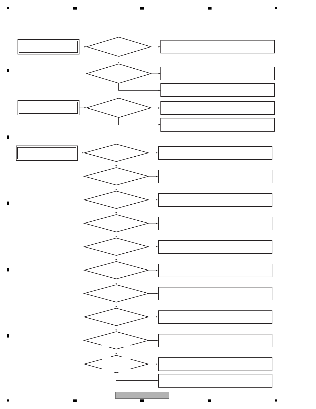
• CD does not work
CD does not work (playback)
• Check connection between each cable.
No
Yes
Is FFC
to connect Pickup Assy and
CD Assy connected?
(MAIN Assy)
(MAIN Assy)
(CD Assy)
• Check whether a cable is arranged neatly.
(A cable do not touch a Disc rotate section)
No
Yes
Is the
cable arranged neatly
arround CD tray section?
• Check the IC311 and its peripheral circuits. (POWER Assy)
No
Yes
Is the
power supply voltage of
the BTL driver (IC1606)
8 V?
(CD Assy)
• Check the IC313 and its peripheral circuits. (POWER Assy)
No
Yes
Is the power
supply voltage of the CD UCOM
(IC1604), CD DSP (IC1601)
3.3 V?
(CD Assy)
• Check the IC1604, X1602 and its peripheral circuits. (CD Assy)
No
Yes
Does
the oscillator (X1602) for
CD UCOM oscillate it?
(CD Assy)
• Check the IC1601, X1601 and its peripheral circuits. (CD Assy)
No
Yes
Does
the oscillator (X1601) for
CD DSP (IC1601) oscillate
it?
(CD Assy)
• Check the IC1601, X1601 and its peripheral circuits. (CD Assy)
No
Yes
Does a
signal output it from CD DSP
(IC1601) pin 14
(DCLK)?
(CD Assy)
• Check the IC1604 and its peripheral circuits. (CD Assy)
• Check the IC601 pin 51 (CD RESET signal). (MAIN Assy)
No
Yes
Is the signal
of CD UCOM (IC1604) pin 40
(CD RESET) "H"?
(CD Assy)
• Check the IC1604 and its peripheral circuits. (CD Assy)
No
Yes
(CD Assy)
• Check the IC1604 and its peripheral circuits. (CD Assy)
No
Yes
• Check the IC1601, IC1606 and its peripheral circuits. (CD Assy)
Does signals
output from CD UCOM (IC1604)
pin 25, 27, 28 (MAIN_BUSY,
CD_RX, CD_TX)?
(CD Assy)
Is the signal
of CD UCOM (IC1604) pin 9
(8035 RESET) "H"?
A
2 3 4
B
C
D
E
F
18
1
2 3 4
X-HM81-K
Page 19
5
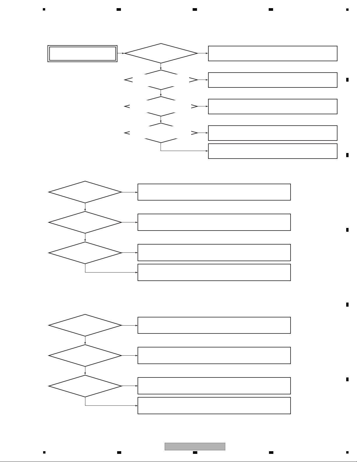
• Check the connection between the BCO Assy and FRONT Assy.
• Check the IC5 and IC13 and its peripheral circuits. (BCO Assy)
Yes
• Replace the LCD MODULE.
Is LCD
power supply normal?
MOD500 Pin 2,29,34
• Check the connection between the BCO Assy and FRONT Assy.
• Check the IC4 and its peripheral circuits. (BCO Assy)
No
No
Yes
Is the
reset signal of LCD normal?
If MOD500-Pin 3 is "H", its
normal.
• Check the connection between the BCO Assy and FRONT Assy.
No
Yes
Are the
other signals of MOD500
normal?
(FRONT Assy)
(FRONT Assy)
• LCD does not lit
• Do not recognize it in Front USB
• Check the connection of Lug wire between the F_USB Assy and F_AUX Assy.
• Replace the CR870 (MODULE on BCO Assy).
No: Both device NG
• Replace the CR870 (MODULE on BCO Assy).
Mass storage
Device is OK, and is only Apple
Device NG?
• Check the connection between the F_USB Assy and BCO Assy.
• Check the IC9 and its peripheral circuits. (BCO Assy)
No
Yes
Yes
Is the 5V
power supply supplied in 5 and
6 Pins of CP500?
• Check the connection between the F_USB Assy and BCO Assy.
• Check the IC12 and its peripheral circuits. (BCO Assy)
• Replace the CR870 (MODULE on BCO Assy).
No
Yes
Is there USB
signal at 3 and 4 Pins of
CP500?
(F_USB Assy)
CD tray does not do working
(OPEN/CLOSE)
• Check connection between each cable.
No
Yes
Are CD Mecha and
CD Assy connected?
(CD Assy)
Yes
(CD Assy)
• Check the IC1601 and its peripheral circuits. (CD Assy)
No
When operating any keys,
does the signals of CD DSP(IC1601)
pin 108, 114 switch to "H" / "L"?
Yes
(CD Assy)
• Check the IC1606 and its peripheral circuits. (CD Assy)
No
When operating any keys,
does the signals of BTL Driver(IC1606)
pin 9, 10 switch to "H" / "L"?
Yes
(CD Assy)
• Check the IC1601 and its peripheral circuits. (CD Assy)
• Replace the CD Deck Motor.
No
When operating any keys,
does the signals of connector (PN1603)
pin 1, 3 switch to H" / "L"?
6 7 8
A
B
C
D
E
F
X-HM81-K
5
6 7 8
19
Page 20
1
iPod video does not display.
• Check the VIDEO SW IC (IC400) and its peripheral circuits.
(TUNER Assy)
• Check connection between each Assy.
No
No
• Check the connection between the DOCKING Assy and
TUNER Assy.
Yes
Yes
Does a
CVBS signal output to
connector (CP400)
pin 3?
Does a
CVBS signal output to
connector (CP4)
pin 2?
• Check the internal circuits of the DOCKING Assy.
• Check the setting of iPod/iPhone that is external connection.
(DOCKING Assy)
(TUNER Assy)
Cannot recognize physical connection of iPod/iPhone.
• Check the path of the iPod DET signal between Pin 1 of CP1 (DOCKING Assy)
and Pin 55 of IC609 (MAIN Assy). ("L" is normal at iPod/iPhone is connected).
Yes
• Replace the CR870 (MODULE on BCO Assy).
Does the Charge LED
light?
• Check the connection between the DOCKING Assy and BCO Assy.
• Check the IC13 and its peripheral circuits. (BCO Assy)
No
No
Yes
Is the
5V power supply supplied
in 23 Pin of CP1?
• Check the connection between the DOCKING Assy and BCO Assy.
• Check the IC12 and its peripheral circuits. (BCO Assy)
• Replace the CR870 (MODULE on BCO Assy).
No
Yes
Is there USB
signal at 25 and 27 Pins of
CP1?
(DOCKING Assy)
• Do not recognize it in iPod Dock
• No Picture (iPod VIDEO)
A
2 3 4
B
C
D
E
F
20
1
2 3 4
X-HM81-K
Page 21
5
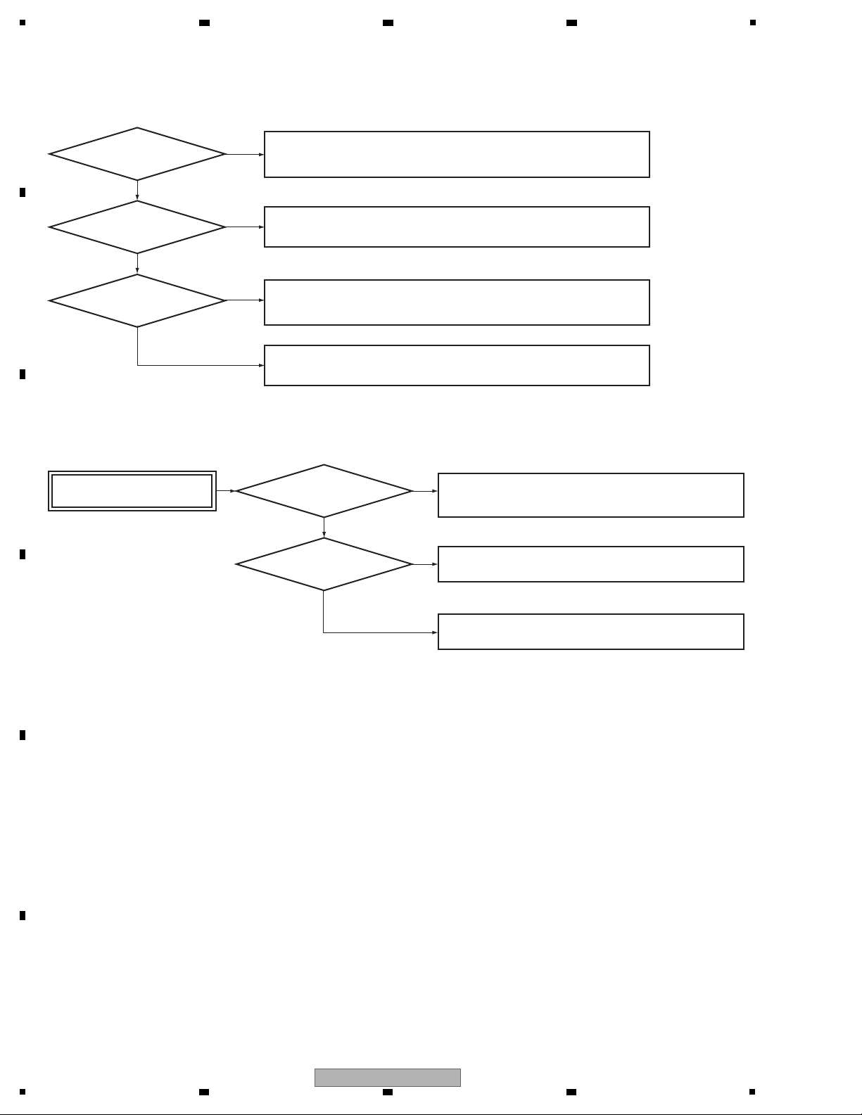
If a protection circuit is activated then the unit enters Standby mode, the LED flashes in accordance with the activated
protection function, as shown in the table below.
The DC outputs from AMP_OUT_L and AMP_OUT_R are detected to avoid DC current surge to the speakers and excess
voltage at B+ (+33 V).
The protection circuit is activated when the signal at Pin 3 of IC601 changes from H to L.
If the DC, POWER, or PWM protection circuit is activated, operation of the unit will be locked.
The buttons that can be used to release operation lock are as follows:
Simultaneously press the "INPUT" and "np" (Tune Up, Skip Up) buttons on the front panel,
or simultaneously press the "STANDBY/ON" and "g" (STOP) buttons on the front panel.
After operation lock is released and the unit is then turned ON, the unit will perform the following:
• Count the number of activations of protection circuits
• Cancel flashing of the LED
Protection
LED ON
DC
POWER
AMP
OVER TEMP1
OVER TEMP2
PWM
BT (*)
100 msec
500 msec
100 msec
100 msec
100 msec
900 msec
100 msec
LED OFF
LED flashing time Operation
Lock
900 msec
500 msec
100 msec
100 msec
100 msec
100 msec
100 msec
Lock
Lock
—
—
—
Lock
*X-HM81,XC-HM81 only
—
USB 100 msec 100 msec —
Description of Each Function
• DC Protect
KTA1268
Q635
R824
100K
B+
KDS4148U
D620
Q639
R867
KTC3198
R827
10K
C731
MTZ22B
100N-K
Q636
KTC3198
R826
47K(1/4)
AMP_OUT_R
AMP_OUT_L
DC_PROTECT
MAIN_MICOM
IC601_3 pin
DC_PROTECT
3
D
MAIN ASSY
M3V3_SW
R602
6 7 8
5.2 PROTECTION CIRCUIT
A
B
C
D
E
F
X-HM81-K
5
6 7 8
21
Page 22
1
The protection circuit is activated when short-circuiting is detected at the regulator output.
The circuit is activated when the signal at Pin 4 of IC601 changes from H to L.
Detected power: B+_27V, B-_27V, AMP_+5V, AMP_-5V, MICOM_3V9, A_+12V, A_-12V, CD_3.3V
Note: The above names are the indications on the POWER Assy. The indications of power may be different on other
Assys.
• Power Protect
The protection circuit is activated when excess current is detected from the AMP.
The circuit is activated when the signal at Pin 78 of IC601 changes from L to H.
• AMP_PROTECT
The protection circuit is activated when abnormally high temperature is detected by the P600 PTC thermistor near IC608
(AMP_Lch).
The circuit is activated when the signal at Pin 92 of IC601 changes from H to L.
• OVER_TEMPERATURE_PROTECT_1
POWER_PROT
M3V3_SW
MAIN_MICOM
IC601_4 pin
POWER_PROT
To
Power supply,
Regulator
4
N
POWER ASSY
F
CNT1 ASSY
D
MAIN ASSY
SELF
MODE1
R606
M3V3_SW
IC608
or
IC612
AMP_PROTECT_DET
MAIN_MICOM
IC601_78 pin
DC_PROTECT
OTP1
78
D
MAIN ASSY
D
MAIN ASSY
R660
M3V3_SW
MAIN_MICOM
IC601_92 pin
OVER_
TEMPERATURE_
PROTECT_1
92
P600 R751R748
A
2 3 4
B
C
D
E
F
22
1
X-HM81-K
2 3 4
Page 23
5
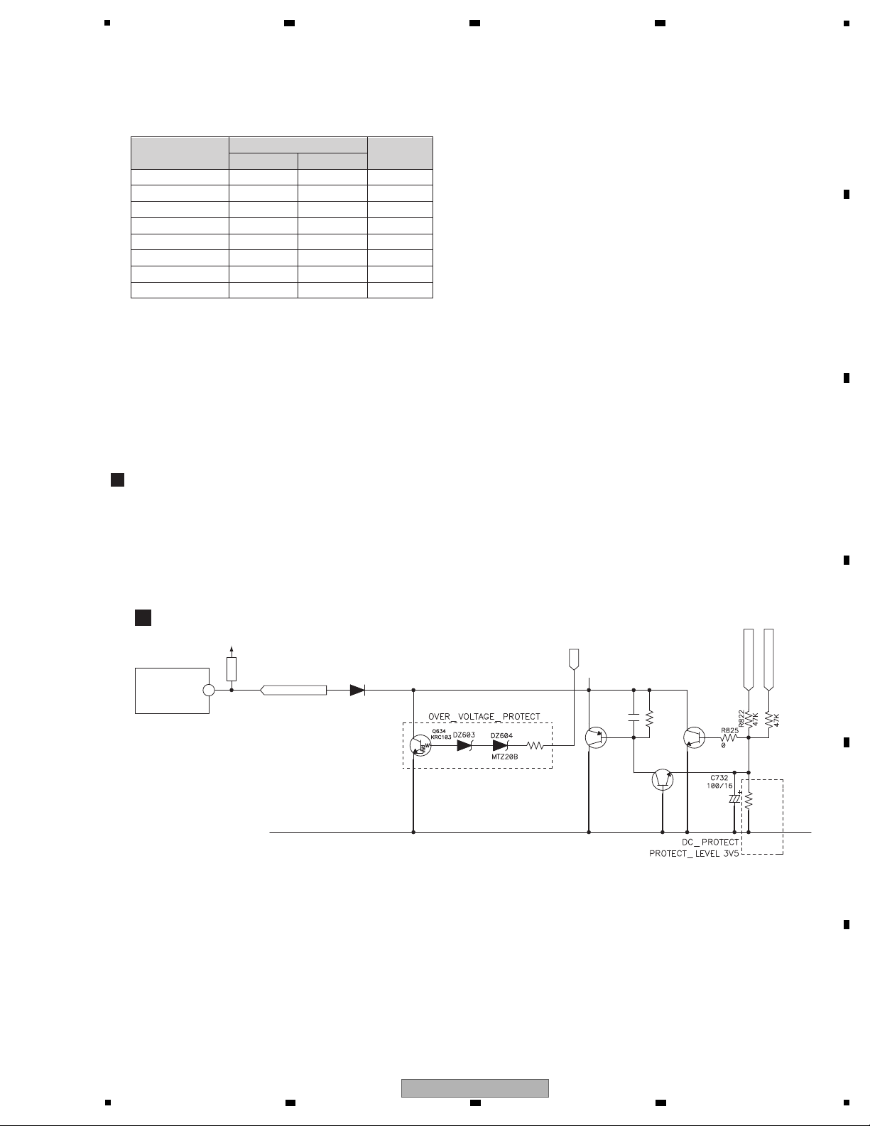
The protection circuit is activated when abnormally high temperature is detected by the P601 PTC thermistor near IC612
(AMP_Rch).
The circuit is activated when the signal at Pin 93 of IC601 changes from H to L.
• OVER_TEMPERATURE_PROTECT_2
D
MAIN ASSY
D
MAIN ASSY
M3V3_SW
MAIN_MICOM
IC601_93 pin
OVER_
TEMPERATURE_
PROTECT_2
93
MAIN_MICOM
IC601_2 pin
DC_PROTECT
2
OTP2
AMP_OUT_R
AMP_OUT_L
PWM_DETECT
P601 R788
M3V3_SW
R608
R787
The protection circuit is activated when abnormally PWM output is detected in the AMP_OUT_L and AMP_OUT_R.
The circuit is activated when the signal at Pin 2 of IC601 changes from H to L.
• PWM_PROTECT
The protection circuit is activated when overcurrent (0.55 A or over) of 5 V power supply supplied in Bluetooth adapter
from ADAPTER PORT terminal is detected.
The circuit is activated when the signal at Pin 104 of IC1 changes from H to L.
• BT_OVERLOAD_PROTECT (X-HM81 and XC-HM81 only)
D619
1SS355
C729
68N
10(1)
R820
R818
27K
1SS355
D621
100K
R821
KTC3875S
Q632
C728
68N
C730
10N
R859
10(1)
BT_OL
D3.3V
DM870
Y14 MICRS
BTSW
IC600_4 pin
C
BT ASSY
E
BCO ASSY
BCO MODULE (CR870)
R256
The protection circuit is activated when overcurrent (USB: 2.1 A or over, iPod Dock: 1 A or over) of 5 V power supply of
Front USB or iPod Dock.
The circuit is activated when the signal at Pin 70 of IC1 changes from H to L.
• USB_OVERLOAD_PROTECT
FAULT
F_USB SW
IC11_8 pin
DOCKING SW
IC14_8 pin
E
BCO ASSY
Y14
DM870
M2 VCO0
BCO MODULE (CR870)
M2
104
IC1
D3.3V
R26
70
IC1
6 7 8
A
B
C
D
5
6 7 8
X-HM81-K
E
F
23
Page 24
1
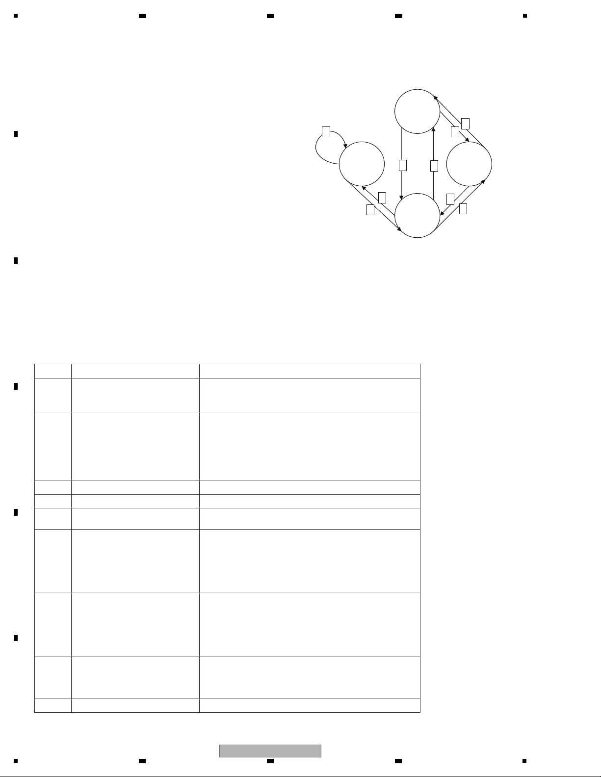
The power supply state transition of this unit becomes the right figure.
Cold Standby:
Mode in which power consumption becomes lowest
Only the main microcomputer among all the microcomputers
is powered.
Power On:
Mode in which AC Relay is turned ON and all microcomputers
are powered
iPod Charge:
Mode in which an iPod is inserted in its dock in modes other
than Power On
In this mode, an iPod device that is plugged into the USB
terminal or the dock can be charged.
The power-supply status is the same as that during
power-on with an HP inserted.
Network Standby:
Mode in which the LCD is unlit with Bco powered in order to
save startup time of Bco
The audio and video output signals are muted, and the keys
and buttons other than the STANDBY/ON key are masked.
Basically, this mode is the same as iPod Charge mode.
Note: The power-off status caused by activation of a protection circuit is not described in this section. See "5.2 Protection circuit."
Cold
Standby
Network
Standby
PowerOn
iPod
Charge
4
1
2
6
5
7
8
3
9
No. Shifting Factor
1 ColdStandby -> Power On
STANDBY/ON on the unit
STANDBY/ON on the remote control unit
WakeUpStart
2 Power On -> ColdStandby
STANDBY/ON on the unit
STANDBY/ON on the remote control unit
Sleep
AutoPowerOff
WakeUpEnd
FactoryReset
3 iPodCharge -> ColdStandby Dock removed
4 ColdStandby -> iPodCharge Dock inserted
5 Power On -> NetworkStandby
NetworkStandby on the remote control unit
ControlAppPowerOff
6 NetworkStandy -> Power On
STANDBY/ON on the unit
STANDBY/ON on the remote control unit
WakeUpStart
ControlAppPowerOn
Air Play started
DMR started
7 iPodCharge -> Power On
STANDBY/ON on the unit
STANDBY/ON on the remote control unit
WakeUpStart
ControlAppPowerOn
Air Play started
DMR started
8 Power On -> iPodCharge
STANDBY/ON on the unit
STANDBY/ON on the remote control unit
Sleep
AutoPowerOff
9 Returning to Network Standby
Removal/insert of the dock
2 3 4
5.3 POWER MANAGEMENT
A
B
C
D
E
F
24
1
X-HM81-K
2 3 4
Page 25
5
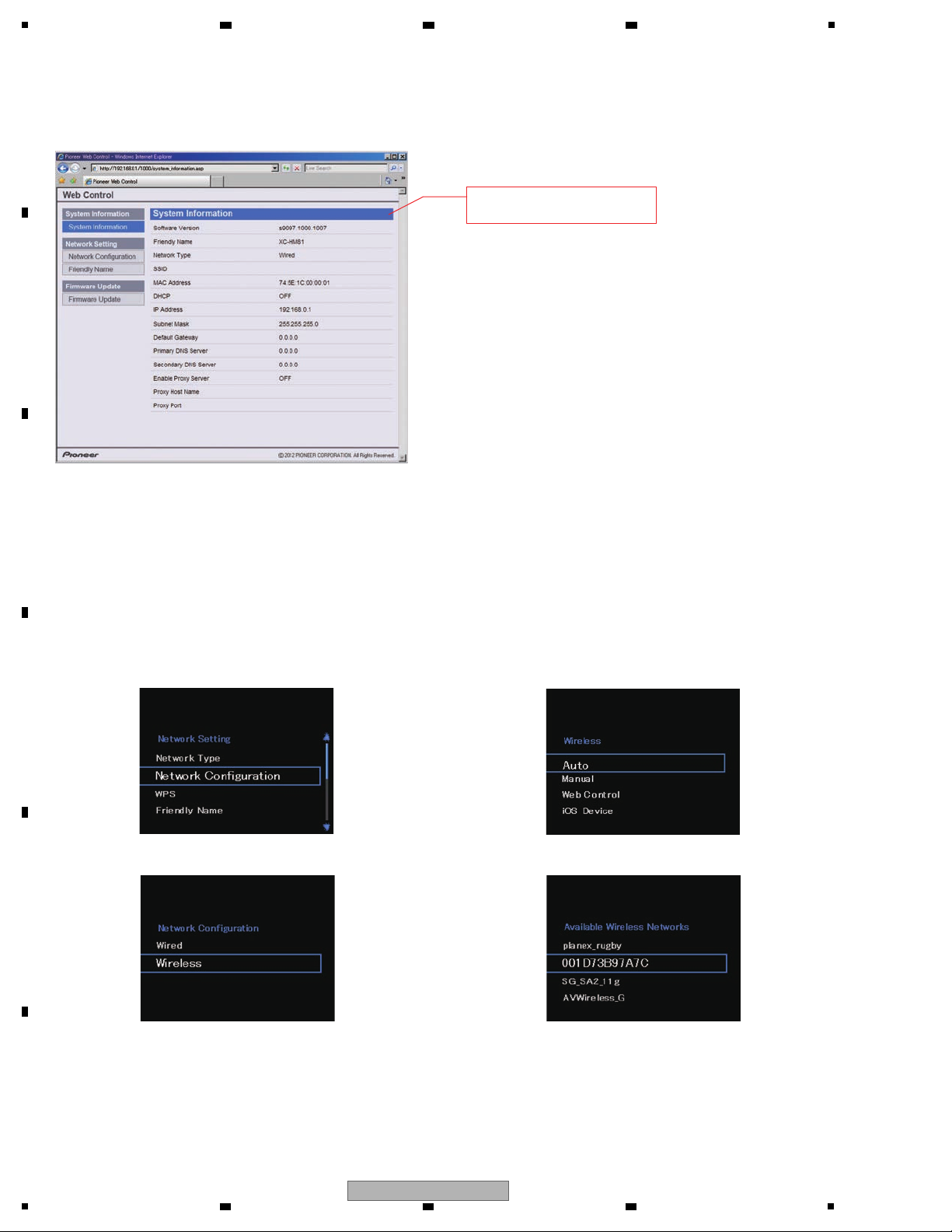
Connect the PC and this unit directly then set them up as indicated below. Then, access this unit from the PC via a Web
browser. If the indications shown in the figure below are displayed, the LAN terminal is normal.
If the LAN terminal is not normal, check the circuit between the LAN terminal and CR870 (Module on BCO Assy).
1 Turn the unit on.
2 Select the NETWORK function then press SETUP.
3 Select Network Setup > Connection Setup > Wired >
DHCP OFF.
4 Set the following items as shown below:
IP address: 192.168.0.1
Subnet mask:255.255.255.0
Gateway address: 0.0.0.0
DNS (1st): 0.0.0.0
DNS (2nd): 0.0.0.0
Proxy setting: Not to be used
5 After setting is finished, reboot the unit.
MAC Address seal
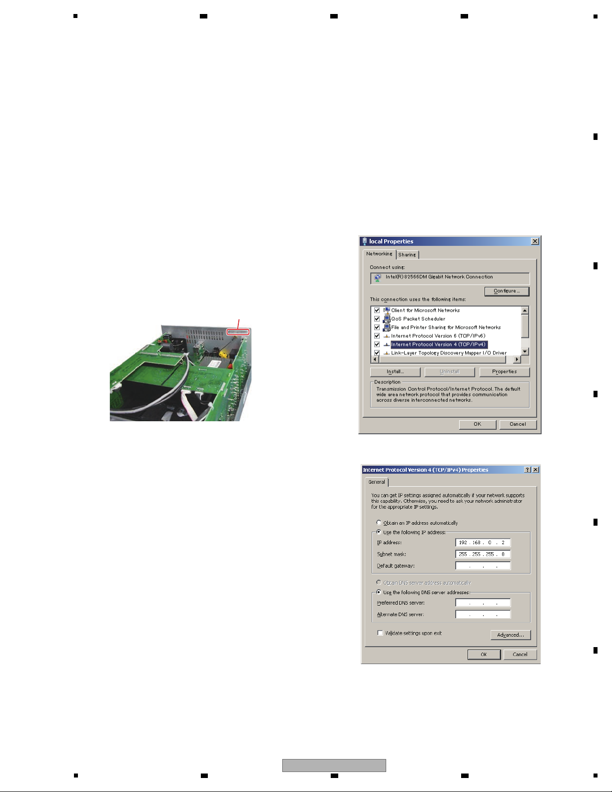
1 Click on Start > Settings > Control Panel.
2 Open Network Connections then Local Area Connection
by double-clicking on its icon.
3 Click on Properties to open the Properties window for
the local area connection.
4 Double-click on Internet Protocol.
1. Checking the LAN terminal
5 Set the items as shown below.
Setup on this unit:
Setup on the PC:
6 7 8
5.4 CHECKING TERMINALS
A
B
C
D
E
F
X-HM81-K
5
6 7 8
25
Page 26
1
Make preparations on the wireless LAN router side then check that the SSID for that router is displayed, following the
procedure shown below. If the SSID is displayed on the LCD, the Wi-Fi antenna works properly.
If the SSID is not displayed, check the wireless LAN antenna, CR870 (Bco Module), and the cable that connects them.
(In the following LCD-display examples, the language setting is English.)
2. Checking the Wi-Fi Antenna
Start the Web browser, input http://192.168.0.1 as a URL. If the screen as indicated below is displayed,
the LAN terminal works properly.
If this screen is displayed,
the LAN terminal works properly.
If the SSID for the prepared router is displayed on the list,
the Wi-Fi antenna works properly.
Note:
As the SSID name for a wireless LAN router supports only
one-byte alphanumerics, if two-byte characters are used in
an SSID name, rename it.
1. Select the NETWORK function then press SETUP.
2. Select Network Setting → Network Configuration.
3. Select Wireless.
4. Select Auto.
5. SSID list is displayed.
A
2 3 4
B
C
D
E
F
26
1
2 3 4
X-HM81-K
Page 27
5
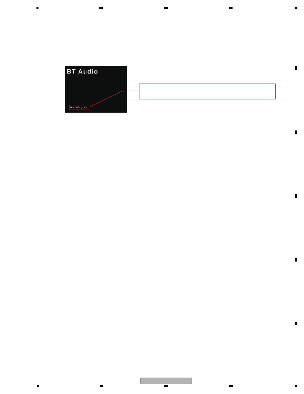
3. Checking the BT Adapter Terminal
If you connect the AS-BT100 or AS-BT200 as shown in the following steps, you can recognize if this unit works properly:
1. Select the BT function, connect the AS-BT100 or AS-BT200, then check that the indication changes as shown in the
figure below.
4. Checking the USB Terminal
This unit is provided with a USB-path switch (IC12) that switches the paths to the CR870, module on BCO Assy, between
the front USB terminal and the upper Docking Terminal, according to the selected function. Accordingly, the behavior of
the USB terminal differs, depending on which path is selected. Therefore, checking is required both with the USB and iPod
functions.
1. Select the USB function then connect an Apple Device (iPod, etc.) to the USB terminal.
If the Apple device is recognized, it is OK.
If "No Data" on the LCD disappears, the device is recognized.
If possible, with the device connected, play a track to check the audio signal for confirmation.
2. Select the iPod function then connect an Apple Device (iPod, etc.) to the USB terminal.
If charging of the Apple device starts, it is OK.
If charging does not start, refer to the diagnosis flowchart for a case in which the USB terminal cannot be recognized on
"5.1 TROUBLESHOOTING".
5. Checking the Docking Terminal
The check procedure is similar to that for "4. Checking the USB Terminal," except for one additional verification.
The Docking Terminal is provided with a function that detects a connection of an Apple device during power-off and starts
charging. This additional function must be also verified.
1. Select the iPod function then put an Apple device (iPod, etc.) in the Dock.
If the Apple device is recognized, it is OK.
If "No Data" on the LCD disappears, the device is recognized.
If possible, with the device connected, play a track to check the audio signal for confirmation.
2. Select the USB function then put an Apple device (iPod, etc.) in the Dock.
If charging of the Apple device starts, it is OK.
3. Disconnect the Apple device from the dock then turn the unit off.
Reconnect the Apple device to the Dock. If the CHARGE LED lights and charging starts, it is OK.
If charging does not start, refer to the diagnosis flowchart for a case in which the Docking Terminal cannot be recognized
on "5.1 TROUBLESHOOTING"..
If the indication does not change as shown in the above figure, possible causes are as follows:
"No Adapter" remains displayed:
The CR870, module on BCO Assy, cannot detect connection of the AS-BT100/200. Check BT_DET.
The indication stops at "Starting":
The CR870, module on BCO Assy, cannot communicate with the AS-BT100/200.
Check power supply to the AS-BT100/200 and the UART communication line.
Signal lines to be checked: BT_ON/CE, BT_+5V, BT_TX/U_RX, BT_RX/U_TX
2. If the indication changes properly in Step 1, perform pairing with a player then check the audio output signals.
If no audio signal is output, check BT_L, BT_R, and BT_MUTE.
After the AS-BT100/200 is connected, the indication will change as follows:
No Adapter -> Starting -> Waiting Device.
6 7 8
A
B
C
D
E
X-HM81-K
5
6 7 8
F
27
Page 28
1
8952HM7100020-IL (UPD78F1166AGF-GAS)(BCO ASSY: IC4)
16-bit Single-chip Microcontrollers
• Pin Function
No. Mark Pin Name I/O Pin Function
1 P60/SCL0 O
2 P61/SDA0 O
3 P62 O
4 P63 XRST_NWONetwork module communication reset
5
P31/TI03/TO03/INTP4
USB_DOCK_OVERLOAD
I Detect that BridgeCo detected a USB overcurrent. Active: L
6 P64/RD USB_DATA_SW O DOCK USB DATA switching output L:USB / H: DOCK
7 P65/WR0 DOCK_RESISTER O ChargeResister control of USB DATA lines of DOCK Active: L
8 P66/WR1 USB_RESISTER O ChargeResister control of USB DATA lines of USB-A Active: L
9 P67/ASTB USB_START I Detect that BridgeCo started USB control. H: Start Active: H
10
P77/EX23/KR7/INTP11
I
11
P76/EX22/KR6/INTP10
DOCK_SEL I USB connection switching request of BridgeCo Active: H
12
P75/EX21/KR5/INTP9
USB_SEL I USB connection switching request of BridgeCo Active: H
13
P74/EX20/KR4/INTP8
HSYNC I HSYNC monitor of LCD communication
14 P73/EX19/KR3 O NC
15 P72/EX18/KR2 XCS_LCD O LCD communication chip select output (Flow control-Subcon request)
16 P71/EX17/KR1 O
17 P70/EX16/KR0 O NC
18 P06/WAIT O NC
19 P05/CLKOUT O NC
20 EVSS1 EVSS1 - Ground of port block (except P20-P27, P110, P111, P121-P124, P150-P157)
21 P80/EX0 DOCK_PWR_ON O DOCK BUS POWER ON/OFF control output Active: H
22 P81/EX1 USB_PWR_ON O USB BUS POWER ON/OFF control output Active: H
23 P82/EX2 O NC
24 P83/EX3 O NC
25 P84/EX4 O NC
26 P85/EX5 O NC
27 P86/EX6 O NC
28 P87/EX7 O NC
29
P30/INTP3/RTC1HZ
VFD_CE O FL CE
30 EVDD1 EVDD1 -
Positive power supply of port block (except P20-P27, P110, P111, P121-P124, P150-P157)
31 P50/EX8 O NC
32 P51/EX9 O NC
33 P52/EX10 O NC
34 P53/EX11 O NC
35 P54/EX12 O NC
36 P55/EX13 USB_DATA_EN O Switch enable output of USB DOCK DATA switch Active: L
37 P56/EX14 O NC
38 P57/EX15 O NC
39
P17/EX31/TI02/TO02
O NC
40
P16/EX30/TI01/TO01/INTP5
O NC
41
P15/EX29/RTCDIV/RTCCL
O NC
42 P14/EX28/RxD3 DEBUG_RX I 232C DEBUG RX
43 P13/EX27/TxD3 DEBUG_TX O 232C DEBUG TX
44
P12/EX26/SO00/TxD0
TX0_DI_NW O Data output of network module communication (Sub->DM860)
45
P11/EX25/SI00/RxD0
RX0_DO_NW I Data input of network module communication (DM860->Sub)
46 P10/EX24/SCK00 CLK_NW O Clock output of network module communication
47 AVREF1 AVREF1 -
48 P110/ANO0 BT_MUTE O BT MUTE Active: L
49 P111/ANO1 CS_NW O Chip select output of network module communication
50 AVREF0 AVREF0 -
2 3 4
5.5 IC INFORMATION
A
B
C
D
E
F
28
1
X-HM81-K
2 3 4
Page 29
5
• Pin Function
No. Mark Pin Name I/O Pin Function
51 AVSS AVSS 52 P157/ANI15 O NC
53 P156/ANI14 O NC
54 P155/ANI13 O NC
55 P154/ANI12 O NC
56 P153/ANI11 O NC
57 P152/ANI10 O NC
58 P151/ANI9 O NC
59 P150/ANI8 O NC
60 P27/ANI7 SUB_IRQ O SUB → MAIN REQUEST output
61 P26/ANI6 O NC
62 P25/ANI5 XRST_LCD O LCD communication reset
63 P24/ANI4 O NC
64 P23/ANI3 O NC
65 P22/ANI2 O NC
66 P21/ANI1 O NC
67 P20/ANI0 O NC
68 P130 O NC
69 P131/TI06/TO06 O NC
70 P04/SCK10/SCL10 CSK_MAIN O Communication clock of MAIN ⇔ SUB
71
P03/SI10/RxD1/SDA10
SCDO_MAIN I Communication data of SUB ← MAIN
72 P02/SO10/TxD1 SCDI_MAIN O Communication data of SUB → MAIN
73 P01/TO00 I NC
74 P00/TI00 REM I IR remote control signal input (NC. only WS)
75 P145/TI07/TO07 PWM_LCD O Backlight control (PWM) of LCD communication
76 P144/SO20/TxD2 DI_LCD O Data output of LCD communication
77
P143/SI20/RxD2/SDA20
DO_LCD I Data input of LCD communication
78
P142/SCK20/SCL20
CLK_LCD O Clock output of LCD communication
79
P141/PCLBUZ1/INTP7
ONC
80
P140/PCLBUZ0/INTP6
ONC
81 P120/INTP0/EXLVI MAIN_REQ I MAIN REQUEST input
82 P47/INTP2 REQ_NW I Request input of network module communication
83
P46/INTP1/TI05/TO05
ONC
84 P45/SO01 O NC
NC
85 P44/SI01 VFD_DI I FL DATA input
86 P43/SCK01 VFD_CLK I
I/O
I/O
FL CLOCK
87 P42/TI04/TO04 O
88 P41/TOOL1 TOOL1 Clock output for debuggers
89 P40/TOOL0 TOOL0
Data input/output for flash memory programmer/debugger
External pull-up for using on-chip debugger.
90 RESET RESET I Reset input
91 P124/XT2 XT2 I
NC When the real-time clock function is not used, connection is not needed. Decide it during W/s.
92 P123/XT1 XT1 I
NC When the real-time clock function is not used, connection is not needed. Decide it during W/s.
93 FLMD0 FLMD0
Pin for flash memory programming mode pull-in
(pull-down in open or more than 100kΩ)
94 P122/X2/EXCLK X2 I Oscillator connection for main system clock
95 P121/X1 X1 I Oscillator connection for main system clock
96 REGC REGC
Connect a stable capacitance of the regulator output (2.5V) for internal operation.
Connected to VSS via a capacitor (0.47-1μF: a target).
97 VSS VSS -
-
-
Ground (except P121-P124 and port block)
98 EVSS0 EVSS0 - Ground of port block (except P20-P27, P110, P111, P121-P124, P150-P157)
99 VDD VDD - Positive power supply (except P121-P124 and port block)
100 EVDD0 EVDD0 -
Positive power supply of port block (except P20-P27, P110, P111, P121-P124, P150-P157)
6 7 8
X-HM81-K
5
6 7 8
A
B
C
D
E
F
29
Page 30
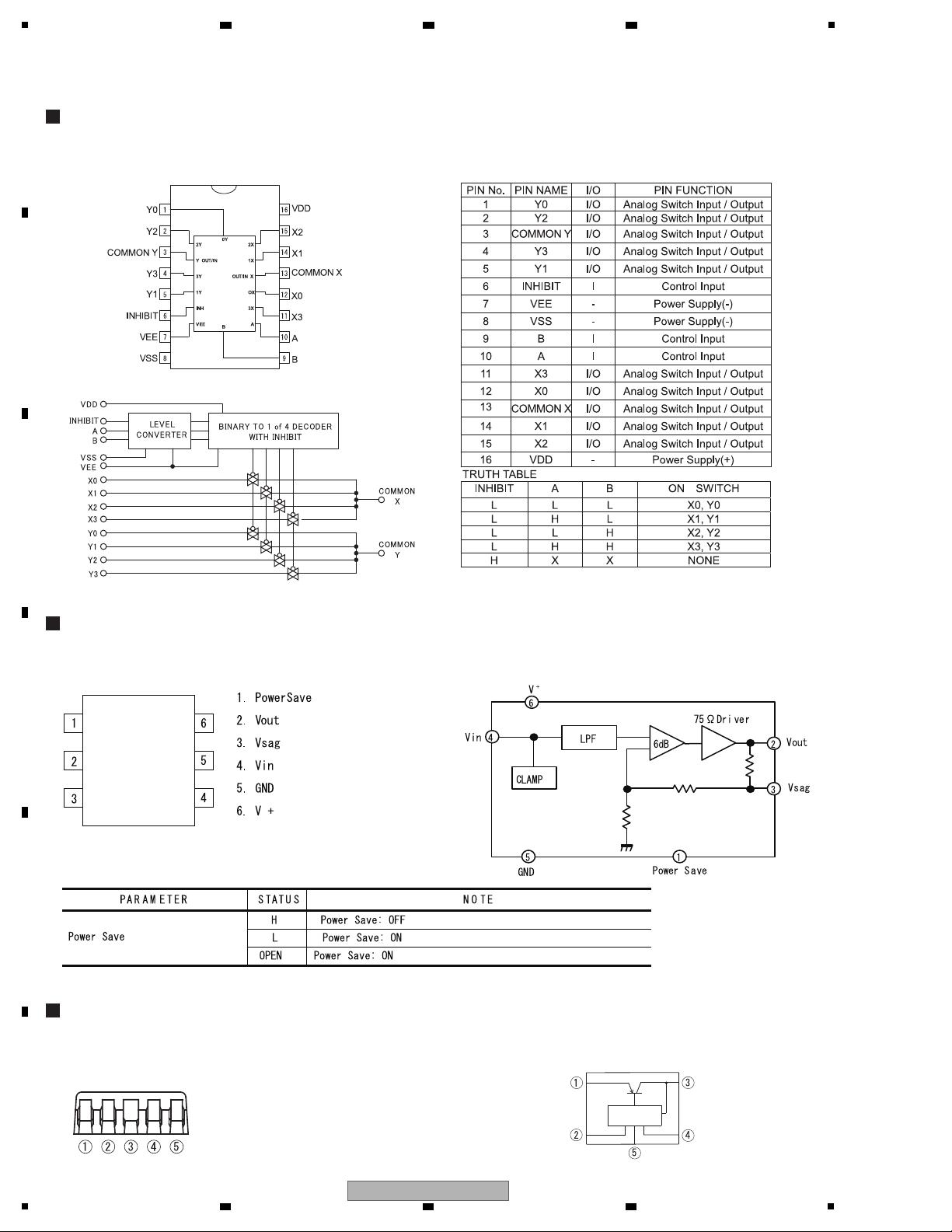
1
(BU4052BCF)(CNT2 ASSY: IC704)
High Voltage CMOS Logic ICs <Analog Switch>
J127256100010-IL (NJM2561)(TUNER ASSY: IC400)
LOW VOLTAGE VIDEO AMPLIFIER WITH LPF
J126012010010-IL (PQ012FZ01ZP)(BCO ASSY: IC2)
Voltage Regurator
• Pin Arrangement
• Block Diagram
• Pin Function
• Pin Arrangement
• Pin Arrangement
• Control Terminal
• Block Diagram
• Block Diagram
DC input (Vin) DC output (Vo)
GND
ON/OFF control (VC)
Specific IC
Bias power supply (VB)
A
2 3 4
B
C
D
E
F
30
X-HM81-K
1
2 3 4
Page 31

5
1. About Service Mode
When the unit enters Service mode, the dedicated Service menu is started. In Service mode, the Service menu is open.
You can perform the following tasks on the Service menu:
· Confirmation of the versions of Bco CPU/Main microcomputer/CD IF microcomputer/CD DSP microcomputer
/Submicrocomputer
· Confirmation of the model information (whether the model name recognized by the software is XC-HM71 or XC-HM81)
· Confirmation of the region information (The region recognized by the software will be displayed.)
· Confirmation of the network information
· Updating the Bco CPU or submicrocomputer via USB
· Resetting to factory default
In Service mode, the protection circuits operate in the same manner as in normal operation.
2. How to Enter Service Mode
Turn the unit on then select the Music Server function.
Press the ESC (A85F) then +10 (A81F) button on the service remote control unit (GGF1381) to activate Service mode.
* If you press any button between the ESC and +10 buttons on the service remote control unit, the unit will not enter
Service mode.
Note: If you enter Service mode with the CD/TUNER function selected, you cannot use cursor operations.
3. How to Quit Service Mode
You can quit Service mode in one of the following ways: (1) switching the function, (2) turning the unit off,
or (3) pressing the k button while the top-layer screen of the Service menu is displayed.
4. Service Menu
For menu operation, use the cursor (i/j/k/l) and ENTER buttons on the remote control unit supplied with this unit.
To register a selection, use the ENTER button. To return to the previous layer, use the k button.
You can perform cursor operation using the buttons on the unit. The top layer of the Service menu is as shown below.
Buttons on the unit Operation
f (PLAY/PAUSE) Select
g (STOP) Undo
np (FWD SKIP) Cursor down
om (REV SKIP) Cursor up
Service Menu
System Information
BcoCPU Update Via USB
Factory Reset
Subcom Update Via USB
4.1 System Information
If System Information is selected, the screen shown below will be displayed.
System Information
BcoCPU Ver.: 1.000
SubCPU Ver.: 1000
Model: XC-HM71
Other.: 1.000 / 1.00 / 1.00
Bco (CR870, module on BCO Assy) Version
Maincom / CD IF / CD DSP
M16C / uPD78F0515 / S5L8035
Model name recognized by the software
XC-HM71 / XC-HM81
Subcom uPD78F166 Version
6 7 8
6. SERVICE MODE
6.1 SERVICE MODE
A
B
C
D
E
5
6 7 8
X-HM81-K
F
31
Page 32

1
4.2 Resetting to Factory Default
If you select Factory Reset then Start on the Service menu, the following screen will be displayed:
Reset?
[SETUP]
[RETURN]
Reset
Cancel
System Information
Region: EU
MAC: 74:5e:1c:06:ab:2d
IP : 192.168.0.1
Region recognized by the software
JPN / EU / CAN / CHN
IP Address: "0.0.0.0" if the unit is not connected to LAN
After resetting to factory default, the unit will shut itself off.
To quit this mode and return to the Service menu
MAC Address: The higher-order values "74:5e:1c" are fixed.
5. Canceling a Power-On Prohibition Status Caused by Activation of a Protection Circuit
The protection circuits indicated below are mounted in this unit. If operation of this unit is locked by activation of any
protection circuit, you can cancel the lock by either of the two methods indicated below.
You can confirm the number of detected activations of protection circuits in Protect Check mode.
For details, see "6.2 PROTECT CHECK MODE" All LEDs are lit in Protect Check mode.
Note:
If any of the Music Server, Internet Radio, or Favorites functions is selected before this unit is started in Protect Check mode,
the selected function screen will be displayed until network connection is established (it may take up to dozens of seconds),
then the Protect Check Mode screen will be displayed.
Example: Startup → Pioneer Logo → Music Server screen → Network established → Protection Check screen
Canceling Operation Lock
np and INPUT buttons of this unit: To cancel operation lock and turn on the unit
g and u STANDBY/ON button of this unit: To cancel operation lock and enter Protect Check mode
Protection Clear Key Operation
Timer LED blink timing
ON ON
DC Special Lock100 ms 900 ms
POWER Special Lock500 ms 500 ms
AMP POWER Clear100 ms 100 ms
OVER TEMP1 POWER Clear100 ms 100 ms
OVER TEMP1 POWER Clear100 ms 100 ms
PWM Special Lock900 ms 100 ms
BT over load POWER Clear100 ms 100 ms
USB over load SPECIAL Clear100 ms 100 ms
A
2 3 4
B
C
D
E
F
32
1
2 3 4
X-HM81-K
Page 33

5
In this mode, detected protection activations are displayed.
Outline
Basic Operation
Explanation
To enter Protect Check mode,
simultaneously press the "g (STOP)"
and "STANDBY/ON" buttons
during Cold Standby.
The last protection activation that
was detected before Protect Check
mode is entered will be displayed.
Unit "g (STOP)"
+
Unit "STANDBY/ON"
Unit "np"
Unit "np"
Unit "np"
Unit "np"
Unit "np"
Key Sequence
LCD Display
6.2 PROTECT CHECK MODE
6 7 8
A
B
C
D
E
5
X-HM81-K
6 7 8
F
33
Page 34

1
After the counts of detected protection
activations for all protection circuits
are displayed, the menu for resetting
the counters will be displayed.
The counters will be reset when the
"f (Play/Pause)" button on the
unit is pressed.
To turn the unit off, press the
"STANDBY/ON" butonn during
Protect Check mode.
Unit "np"
Unit "np"
Unit "np"
Unit "np"
Unit
"f (Play/Pause)"
Unit "STANDBY/ON"
Auto
Unit
"np"
During Protect Check mode, response to keys other than those described below is disabled.
Unit "np" button
Unit "f (Play/Pause)" button
Unit "STANDBY/ON" button
Remarks
Explanation Key Sequence LCD Display
A
2 3 4
B
C
D
E
F
34
X-HM81-K
1
2 3 4
Page 35

5
To enter Test mode, select the NETWORK function, then press the ESC then FRM/TIM keys.
TEST MODE will be displayed. (Although TEST MODE is displayed even if the CD or Tuner function
is selected, LCD checking is not possible with those functions selected.)
LCD checking is possible in Test mode for use on the production line.
To quit TEST MODE, perform one of the following operations:
1. Switch the input function.
2. Turn the unit off.
3. Perform factory setting.
How to perform LCD checking
Each time the 1 key on the remote control unit supplied with the product is pressed, the screen is changed as shown below
Ramp > Black > White > Red > green > Blue
If the 0 key is pressed, the screen will return to that of playback.
[Screens to be displayed]
6 7 8
6.3 CHECKING THE LCD
A
B
C
D
E
F
X-HM81-K
5
6 7 8
35
Page 36

1
This unit can display all the characters that are indicated in the white cells in the table below properly but cannot display the
characters in gray cells properly and will indicate such characters as "#." Those are the characters shown below in the RDS
standard:
0x5E
0x60
0x7E
2 3 4
6.4 RDS CHARACTERS
A
B
C
D
E
F
36
1
2 3 4
X-HM81-K
Page 37

5
[1] Cabinet and DOCKING Assy
(1) Remove the eight screws.
(K: B020030083F10-IL)
(S: BBZ30P080FNI)
Note:
(1) Do NOT look directly into the pickup lens. The laser beam may cause eye injury.
(2) Even if the unit shown in the photos and illustrations in this manual may differ from your product, the
procedures described here are common.
(3) For performing the diagnosis shown below, the following jigs for service is required:
• BtoB extension jig cable (GGD1770) • 3P Extension jig cable (GGD1773)
• BtoB extension jig cable (GGD1810) • 4P Extension jig cable (GGD1809)
• BtoB extension jig cable (GGD1811) • Extension jig FFC (GGD1774)
• BtoB extension jig cable (GGD1812) • FPC Extension jig (GGD1813)
• Cabinet
1 1 1 1
1
1
1
1
• Rear view
Cabinet
Cabinet
(2) Remove the cabinet.
Note:
Please do not damage the cables when removing
the cabinet.
Cabinet
2
6 7 8
7. DISASSEMBLY
A
B
C
D
E
F
X-HM81-K
5
6 7 8
37
Page 38

1
• DOCKING Assy
(1) Disconnect the one connector.
(CP4)
(2) Remove the shield plate-iPod by removing the
two screws.
(B020030081B10-IL)
(3) Remove the DOCKING Assy by unhooking the
two hooks.
2 2
33
1 1 1
2
4
4
5
5
6
2
3
3
1
• Bottom view
• Bottom view
• Bottom view
DOCKING Assy
Front panel section
CNT3 Assy
Shield plate-iPod
Cabinet
CP4
FPC2
CP607
[2] Front Panel Section
(1) Remove the three screws.
(K: B020030083F10-IL)
(S: B020030084F10-IL)
(2) Remove the two screws.
(B020030084F10-IL)
(3) Unhook the two hooks.
(4) Disconnect the one flexible cable and one
connector.
(FPC2, CP607)
(5) Remove the two screws.
(B020030084F10-IL)
(6) Remove the front panel section.
(1) Remove the cabinet.
(See procedure [1].)
A
B
2 3 4
C
D
E
F
38
1
X-HM81-K
2 3 4
Page 39

5
(7) Disconnect the two connectors.
(CP500, 602)
[3] Back Chassis
(1) Remove the one cushion.
(2) Remove the 13 screws. (BBT30P100FTB)
(for X-HM81 and XC-81M)
(2) Remove the 11 screws. (BBT30P100FTB)
(for X-71HM)
(3) Remove the back chassis.
(1) Remove the cabinet.
(See procedure [1].)
FRONT Assy
F_USB Assy KEY AssyF_AUX Assy
7
7
CP500
CP602
1
2
2
2
2
222
2
2
2
22
2
• Rear view
Back chassis
X-81HM, XC-81HM
only
X-81HM, XC-81HM
only
3
6 7 8
A
B
C
D
E
F
X-HM81-K
5
6 7 8
39
Page 40

1
[4] CNT3 Assy, CD Assy and MECHA
(1) Remove the cabinet.
(See procedure [1].)
(2) Remove the front panel section.
(See procedure [2].)
(1) Disconnect the four BtoB connectors.
(CP18, 19, 30, 31)
(2) Remove the CNT3 Assy.
• CNT3 Assy
(3) Disconnect the two BtoB connectors.
(PN1701, 1702)
(4) Remove the CD Assy.
(5) Short-circuit position of figure solodering.
(short)
Note:
After working, connect the flexible cable,
then remove the soldered joint (open).
(6) Disconnect the one flexible cable.
(PN1602)
• CD Assy
CNT3 Assy
CD Assy
CD Assy
PN1701
CP19
CP18
CP31 CP30
PN1702
1
2
1
4
1 1
3
3
MECHA
PN1602
6
5
A
B
2 3 4
C
D
E
F
40
1
X-HM81-K
2 3 4
Page 41

(7) Remove the four screws.
(B020230083B10-IL)
(8) Remove the MECHA.
• MECHA
7
7
7
7
MECHA
8
[5] MAIN Assy
(1) Remove the cabinet.
(See procedure [1].)
(2) Remove the front panel section.
(See procedure [2].)
(3) Remove the back chassis.
(See procedure [3].)
(4) Remove the CNT3 and CD Assemblies.
(See procedure [4].)
(1) Remove the one screw.
(B020230083B10-IL)
(2) Disconnect the one BtoB connector.
(CP605)
(3) Remove the MAIN Assy.
• MAIN Assy
1
Front side
• Bottom view
MAIN Assy
CNT1 Assy
CP605
2
3
5
6 7 8
A
B
C
D
5
X-HM81-K
6 7 8
E
F
41
Page 42

1
(1) Connect the extension jig FFC to MECHA.
GGD1774: MECHA ↔ CD (PN1602)
(2) Reassemble the front panel section.
(3) Connect the each jig cables.
GGD1770: CD (PN1705) ↔ POWER (CP310)
GGD1773: CNT2 (CN511) ↔ MAIN (CP512)
GGD1809: FRONT (CN515) ↔ CNT3 (CP607)
GGD1810: CNT2 (CP505, 506) ↔ CNT3 (CP30, 31)
GGD1811: CNT1 (CP712) ↔ MAIN (CP605)
GGD1812: CD (PN1702) ↔ MAIN (CP604)
GGD1813: FRONT (FPC515) ↔ CNT3 (FPC2)
(4) Insert the any insulation sheet.
• Diagnosis
PN1602
PN1705
PN1702
CP310
CP607
FPC2
CP605
CP512
CN511
CP712
CP604
CP30
CP506 CP505
CP31
CD Assy
Insulation sheet
4
POWER Assy
Cut it
Extension jig FFC
(GGD1774)
Extension jig cable
(GGD1770)
1
Front panel section
CNT2 Assy
MAIN Assy
2
3
Extension jig cable
(GGD1773)
3
CNT3 Assy
Extension jig cable
(GGD1809)
Make sure to insert
correctly.
Make sure to match
the color of cord.
3
Extension jig + FFC
(GGD1813)
3
Extension jig cable
(GGD1812)
3
Extension jig cable
(GGD1811)
3
Extension jig cable
(GGD1810)
3
[6] BCO Assy
(1) Remove the cabinet.
(See procedure [1].)
(4) Remove the CNT3 Assy.
(See procedure [4].)
(3) Remove the back chassis.
(See procedure [3].)
(1) Release the two jumper wires.
(2) Remove the TUNER Assy by disconnecting
the one BtoB connector.
(CP400)
• TUNER, CNT2 and BCO Assy
CNT2 Assy
TUNER Assy
2
1
1
CP400
A
2 3 4
B
C
D
E
F
42
1
X-HM81-K
2 3 4
Page 43

5
(3) Remove the CNT2 Assy by disconnecting
the two BtoB connectors.
(CP11, 12)
(4) Remove the BCO_STOPPER Assy by
removing the two screws.
(B020030171B10-IL)
(5) Remove the BCO Assy.
CNT2 Assy
BCO Assy
BCO_STOPPER Assy
3
5
CP11 CP12
4 4
(1) Connect the extension jig FFC to MECHA.
GGD1774: MECHA ↔ CD (PN1602)
(2) Connect the each jig cables.
GGD1770: CD (PN1705) ↔ POWER (CP310)
GGD1773: CNT2 (CN511) ↔ MAIN (CP512)
GGD1810: CNT2 (CP505, 506) ↔ CNT3 (CP30, 31)
GGD1812: CD (PN1702) ↔ MAIN (CP604)
(3) Insert the any insulation sheet.
• Diagnosis
CP512
CN511
CP604
CP506
CP505
CP30
CP31
CD Assy
POWER Assy
CNT3 Assy
CNT2 Assy
BCO Assy
PN1602
Extension jig FFC
(GGD1774)
1
PN1702
PN1705
CP310
Insulation sheet
3
Cut it
Extension jig cable
(GGD1770)
2
Extension jig cable
(GGD1812)
2
Extension jig cable
(GGD1810)
2
Make sure to match
color of cord.
Make sure correctly to conect this
cord to BCO Assy as this cord can
be conected to opposite side.
(It may cause to break circuit in
case of wrong connection. )
Extension jig cable
(GGD1773)
2
6 7 8
A
B
C
D
E
F
5
6 7 8
X-HM81-K
43
Page 44

1
[7] POWER Assy
(1) Remove the cabinet.
(See procedure [1].)
(2) Remove the front panel section.
(See procedure [2].)
(3) Remove the back chassis.
(See procedure [3].)
(4) Remove the CD PCB Assy.
(See procedure [4].)
(1) Remove the two screws.
(B020230083B10-IL)
(2) Remove the two screws.
(B028940101B11-IL)
(3) Remove the three screws.
(B020230083B10-IL)
(4) Remove the two screws.
(B028940101B11-IL)
(5) Remove the POWER Assy by disconnecting
the one BtoB connector.
(CP312)
• How to Reassemble the POWER Assy
Place the POWER Assy so that the rear side of the POWER Assy comes in contact with that of the chassis,
then secure the four fastening screws of the transformer.
1
1
2 2
3
4 4
Front side
Rear side
• Bottom view
POWER Assy
×3
5
Back chassis
Chassis
Bring the POWER Assy into contact
with the bend of the chassis.
Rationale:
If the POWER Assy is not assembled as described above, it will be attached nearer to the front than as designed,
with the result that the cabinet and the rear panel may be separated by a gap or that the front panel may be inclined forward.
CP312
POWER Assy
Transformer
A
B
2 3 4
C
D
E
F
44
1
2 3 4
X-HM81-K
Page 45

5
[Purpose]
PC
UPDATE jig
GGF1642
RS-232C
Straight cable
10P
10P
Refer to this section when updating the firmware of each microcomputer is required by the service information, etc.
[Necessary T ools]
• PC with a serial port
• Updating program: FlashSta.exe
• RS-232C straight cable (9pin female ↔ 9pin male)
• RS-232C update jig: GGF1642
• Firmware file: ".mot" file
[Connections]
Remove the cabinet (bonnet) so that the MAIN Assy becomes accessible.
Connect as shown in the figure below.
For the contact side of the FFC, see the photo below.
[Procedures]
1. Unplug the Power cord.
Connect the FFC cable. ( MAIN microcomputer )
Start up application FlashSta on the PC.
3. Press the OK button.
[ if the following messages are displayed ]
Please push the cancel button and press the JIG's
RESET button.
And confirm a connection of FFC.
Please return to procedure 1.
2. Plug the Power cord. (STANDBY mode)
For updating of the MAIN microcomputer, proceed with
the following steps in STANDBY mode.
MAIN Assy (side A)
Front side
Contact side
Select for COM port.
Updating of the MAIN Microcomputer firmware
6 7 8
8. EACH SETTING AND ADJUSTMENT
8.1 UPDATING OF THE FIRMWARE
A
B
C
D
E
5
6 7 8
X-HM81-K
F
45
Page 46

1
4. Select the update file and enter ID. 6. Update Finished MAIN microcomputer.
5. Set speed update and update the MCU.
1 Selection of upgrade file
1 Select the update file
2 Enter ID.
Select "XM** Main V0xx.mot" file
to update the MCU.
2 Enter ID.
Enter "ff" in all field.
Press the OK button.
Press the OK button.
(Default Baud rate is 9600)
Set Baud rate to 38400.
Press the OK button.
Press the OK button. Press the Exit button.
Please wait for until this window
disappears.
3 Press OK button to
go to next step.
2 Update the MCU.
E.P.R=>Erase+Program+Read
2 Update the MCU
Press the E.P.R … button
1 Set speed of update.
1 Set speed of update.
Press OK button.
7. Turn the unit off. (STANDBY mode)
Disconnect the Power cord.
Disconnect the FFC cable.
A
2 3 4
B
C
D
E
F
46
1
X-HM81-K
2 3 4
Page 47

5
Updating of the Subcom, BCO firmware
Subcom update screen
Explanation
1 Save the update files for Subcom (HM71_81_Sub_***.bcd) and for BCO (HMx2013APP****.bcd) in the root folder of
the USB memory.
* Do not change the file name from a file name when it was released.
2 Plug the power cord into the receptacle and turn on the power.
3 Connect the USB memory in which the update file has been stored to the Product.
4 Press “ESC” → “+10” buttons from service remote control unit (GGF1381) and enter into the Service Mode.
5 Select “Subcom Update Via USB” or “BcoCPU Update Via USB” on the Menu Screen.
6 Press on the “ENTER” button on the Update Screen, and the update starts.
7 When update is completed, become the Complete display.
(After the BCO update end, restart automatically. After the Subcom update end, it is necessary to pull out power
cord after display in "Completed!".)
8 Pull out power cord, and put it, and do it, and restart once.
Confirm that Subcom, BCO are revised by "System Information" of "6.1 SERVICE MODE" menu.
Note: Do not plug off the power cord during the update processing.
If you select ENTER on this screen,
updating will start.
To return to the previous screen,
select RETURN.
[ENTER]
[RETURN]
[Procedure]
Key operation
TimeDisplay screen
Updating in progress,
don’t unplug!
[ENTER]
[RETURN]
An alarm message will be displayed
if no updater file is found in the USB
memory. Select ENTER, return to
Service Menu, then retry using the
USB memory in which the updater file
is stored.
* The same message will be displayed
if no USB memory is plugged in.
[ENTER]
[RETURN]
File Not Found
[ENTER] OK
Updating of uPD78F1166 starts and
the message "Updating in progress"
is displayed.
Key operation
disabled
Approx. 5 min.
Updating in progress,
don’t unplug!
"Completed!" is displayed after
updating is completed.
Completed!
6 7 8
A
B
C
D
E
5
X-HM81-K
6 7 8
F
47
Page 48

1
BCO update screen
Explanation
If you select ENTER on this screen,
updating will start.
To return to the previous screen,
select RETURN.
[ENTER]
[RETURN]
The following icons
will be displayed,
according to the
actual status:
Muting icon
Sleep icon
LAN icon
The following icons
will be displayed,
according to the
actual status:
Muting icon
Sleep icon
LAN icon
Key operation TimeDisplay screen
Updating in progress,
don’t unplug!
[ENTER]
[RETURN]
An alarm message will be displayed
if no updater file is found in the USB
memory. Select ENTER, return to
Service Menu, then retry using the
USB memory in which the updater file
is stored.
* The same message will be displayed
if no USB memory is plugged in.
[ENTER]
[RETURN]
File Not Found
[ENTER] OK
Approx. 20 sec.
DM870 will automatically restart.
DM870 is included in CR870, module on
BCO Assy.
Key operation
disabled
Approx. 20 sec.
After restart of DM870 is completed,
the background will be displayed.
Key operation
disabled
After restart is completed, the
updating process will automatically
start.
The progress of updating will be
displayed with the progress bar.
Key operation
disabled
In units of 20%
OK
A
B
2 3 4
C
D
E
F
48
1
X-HM81-K
2 3 4
Page 49

5
Explanation Key operation TimeDisplay screen
Unlimited
When updating is successfully
finished, the color of the progress bar
changes to green and restart will
automatically begin.
If downloading fails, the color of the
progress bar changes to red.
This screen remains displayed if
updating fails. For recovery, unplug
the power cord then plug it back in.
The unit will start with the previous
version of the program.
Updating may fail if the updater file
has erroneous data.
Key operation
disabled
6 7 8
A
B
C
D
E
F
X-HM81-K
5
6 7 8
49
Page 50

1
For updating firmware for the CD I/F and CD DSP microcomputers, create separate discs for updating each microcomputer
then play the disc on the unit.
1. Write a ***.UPG file onto a CD-R/RW to create the disc for updating.
Examples of file names (File names vary, depending on the version of firmware.)
For the CD I/F microcomputer: HM71_81CD_IFM_V1_00_110713.UPG
For the CD DSP microcomputer: HM71_81CD_DSP_V102_(20110720_VT).UPG
File writing can be performed, using the writing function of Windows XP.
Note: Create separate discs for updating the CD I/F and CD DSP microcomputers.
If two files for updating these microcomputers are written on one disc, a problem may occur.
NEVER write files other than a .UPG file onto the CD-R/RW for updating.
2. Turn the unit ON.
3. Set the Function selection to CD.
4. Open the disc tray, load the created disc, then close the tray.
5. Updating starts automatically.
6. After updating is completed, the disc tray will be automatically opened.
7. Unload the disc then turn the unit OFF.
How to Update
Updating of the CD I/F, CD DSP Microcomputers firmware
A
2 3 4
B
C
D
E
F
50
X-HM81-K
1
2 3 4
Page 51

Setting Name Initial Setting Setting Range
NetStandby
Cold
FactoryReset
Storage Place
SETUP
system
Dimmer LEVEL3 LEVEL3 / LEVEL2 / LEVEL1
Memorized Memorized
Clear Maincom
AutoPowerDown
Europe 6h
Off / 2h / 4h / 6h
Memorized Memorized
Clear Maincom
Other countries
Off
Language
Japan Japan English,Japanese
Memorized Memorized
Clear MaincomChina China Chinese
Other countries
English
English, French, German, Dutch, Italian, Spanish, Russian
SOUND
system
SOUND FLAT
FLAT, GAME, CLASSIC, POPS, VOCAL, JAZ
Memorized Memorized
Clear Maincom
P.BASS Off On / Off
Memorized Memorized
Clear Maincom
BASS 0 -5 to +5
Memorized Memorized
Clear Maincom
TREBLE
HM71 +1
-5 to +5
Memorized Memorized
Clear Maincom
HM810
Volume 0 0 to 50
Memorized Memorized
Clear Maincom
SYSTEM FUNCTION iPod All functions
Memorized Memorized
Clear Maincom
12h/24h 24h 12h / 24h
Memorized Memorized
Clear Maincom
CLOCK 0:00:00 Sun
Memorized Memorized
Clear Maincom
TIMER Off / CD / 0:00:00 / EVERYDAY / Vol.0
Memorized Memorized
Clear Maincom
TUNER BAND FM STEREO FM STEREO / FM MONO / AM
Memorized Memorized
Clear Maincom
PRESET Minimum FM frequency 40 Preset
Memorized Memorized
Clear Maincom
PresetName Null 8 characters (ASCII)
Memorized Memorized
Clear Maincom
AM Frequency
Europe 522 522-1602 (9kStep)
Memorized Memorized
Clear Maincom
Japan 522 522-1620 (9kStep)
Canada 530 530-1710 (10kStep)
China 522 522-1620 (9kStep)
FM Frequency
Europe 87.5 87.5-108.00 (50kStep)
Memorized Memorized
Clear Maincom
Japan 76.0 76.0-90.00 (100kStep)
Canada 87.5 87.5-108.00 (100kStep)
China 87.5 87.5-108.00 (50kStep)
NETWORK Network Type Auto Wired / Wireless / Auto
Memorized Memorized
Clear DM870
SSID (Null) 32 characters
Memorized Memorized
Clear DM870
Security None
None / WEP / WPAPSK TKIP / WPAPSK AES
Memorized Memorized
Clear DM870
WPA2PSK TKIP / WPA2PSK AES
WPA Password / WEP Key (Null) 100 characters
Memorized Memorized
Clear DM870
DHCP On On / Off
Memorized Memorized
Clear DM870
IP 0.0.0.0 0.0.0.0 to 255.255.255.255
Memorized Memorized
Clear DM870
SubNetmask 255.0.0.0 0.0.0.0 to 255.255.255.255
Memorized Memorized
Clear DM870
Gateway 0.0.0.0 0.0.0.0 to 255.255.255.255
Memorized Memorized
Clear DM870
DNS1 0.0.0.0 0.0.0.0 to 255.255.255.255
Memorized Memorized
Clear DM870
DNS2 0.0.0.0 0.0.0.0 to 255.255.255.255
Memorized Memorized
Clear DM870
Proxy setting Don't Use Don't Use/Use
Memorized Memorized
Clear DM870
Proxy Server (Null) 128 characters
Memorized Memorized
Clear DM870
Proxy Port (Null) 0 to 65535
Memorized Memorized
Clear DM870
Friendly Name *1 63 characters
Memorized Memorized
Clear DM870
Parental Lock Off On / Off
Memorized Memorized
Clear Maincom
Parental Lock Password 0000 0000 to 9999
Memorized Memorized
Clear DM870
Favorite 0 broadcast station 64 broadcast station
Memorized Memorized
Clear DM870
Internet Radio Last Play (Null) 1 broadcast station
Memorized Memorized
Clear DM870
BT Air Jam Air Jam Off Air Jam On / Air Jam Off
Memorized Memorized
Clear DM870
PIN CODE
If the AC power cable is unplugged before the settings that have been changed are registered, registration of the changed settings will not be guaranteed.
*1 The initial setting is the unit's model name; i.e., XC-HM81 if the unit is a high-end model, or XC-HM71 if the unit is a low-end model.
0000 0000 / 1234 / 8888
Memorized Memorized
Clear DM870
5
8.2 INITIAL SETTINGS
6 7 8
A
B
C
D
E
5
X-HM81-K
6 7 8
F
51
Page 52

1
NOTES: - Parts marked by “NSP” are generally unavailable because they are not in our Master Spare Parts List.
-
The > mark found on some component parts indicates the importance of the safety factor of the part.
Therefore, when replacing, be sure to use parts of identical designation.
-
Screws adjacent to b mark on product are used for disassembly.
-
For the applying amount of lubricants or glue, follow the instructions in this manual.
(In the case of no amount instructions, apply as you think it appropriate.)
SET
SET
(side)
Top Bottom
Front
Polybag packing style
• CD Receiver • Speaker
• Speaker
S-HM81GB (for X-HM81/SYXE8),
S-HM81SA (for X-HM71-S/AXQ5)
• Speaker
S-HM71 (for X-HM71)
Tape (clear)
Tape
(10 x 100)
(clear)
Power cord
Polybag packing style
Front
Speaker
S-HM81GB, S-HM81SA
(for X-HM81)
Speaker
S-HM71
(for X-HM71)
AAA size IEC R03
dry cell batteries
or or
SYXE8
only
Except
CXE
2 3 4
9. EXPLODED VIEWS AND PARTS LIST
A
9.1 PACKING SECTION
B
C
D
E
F
52
1
X-HM81-K
2 3 4
Page 53

5
(1) PACKING SECTION PARTS LIST
Mark No. Description Part No.
1 Remote Control See Contrast table (2)
2 WLAN antenna E600223170010-IL
3 AM Loop Antenna E601019000010-IL
4FM Wire Antenna E605010140010-IL
Operating Instructions (CD-R OM )
5
See Contrast table (2)
6 7 8
No. Description Part No.
Mark
11 Cushion, Snow 6230213174000-IL
12 PE, Sheet 6327210009000-IL
13 • • • • •
14 • • • • •
15 Speaker Wires See Contrast table (2)
A
Operating Instructions
6
Operating Instructions
7
See Contrast table (2)
See Contrast table (2)
8Quick Start Guide See Contrast table (2)
NSP 9 Warranty Card See Contrast table (2)
10 Box, Gift See Contrast table (2)
16 Non Skid Pad See Contrast table (2)
17 Snow Cushion See Contrast table (2)
18 Soft Sheet See Contrast table (2)
19 Soft Sheet See Contrast table (2)
20 Speaker Wires See Contrast table (2)
21 Snow Cushion See Contrast table (2)
22 Bag Poly See Contrast table (2)
(2) CONTRAST TABLE
X-HM81-K/SYXE8, X-HM81-S/SYXE8, XC-HM81-K/SYXE8, XC-HM81-S/SYXE8, X-HM71-K/SYXE8, X-HM71-K/CXE,
X-HM71-S/SYXE8 and X-HM71-S/AXQ5 are constructed the same except for the following:
Mark No. Symbol and Description X-HM81-K/SYXE8 X-HM81-S/SYXE8 XC-HM81-K/SYXE8 XC-HM81-S/SYXE8
1 Remote Control 8300767600010-IL 8300767600010-IL 8300767600010-IL 8300767600010-IL
5 Operating Instructions (CD-ROM) 6517000000821-IL 6517000000821-IL 6517000000821-IL 6517000000821-IL
6 Operating Instructions (En, Fr) Not used Not used Not used Not used
7 Operating Instructions (Zhcn) Not used Not used Not used Not used
8Quick Start Guide 5707000006941-IL 5707000006941-IL 5707000006941-IL 5707000006941-IL
NSP 9 Warranty Card ARY7158 ARY7158 ARY7158 ARY7158
10 Box, Gift 6007212120210-IL 6007212120200-IL 6007212110030-IL 6007212110020-IL
15 Speaker Wires 8952SHM810016-IL 8952SHM810016-IL Not used Not used
16 Non Skid Pad 8952SHM810018-IL 8952SHM810018-IL Not used Not used
17 Snow Cushion 8952SHM810040-IL 8952SHM810040-IL Not used Not used
B
C
18 Soft Sheet 8952SHM810020-IL 8952SHM810020-IL Not used Not used
18 Bag Poly Not used Not used Not used Not used
19 Soft Sheet 8952SHM810030-IL 8952SHM810030-IL Not used Not used
20 Speaker Wires Not used Not used Not used Not used
21 Snow Cushion Not used Not used Not used Not used
22 Bag Poly Not used
Not used Not u
sed Not used
Mark No. Symbol and Description X-HM71-K/SYXE8 X-HM71-S/SYXE8 X-HM71-K/CXE X-HM71-S/AXQ5
1 Remote Control 8300767600010-IL 8300767600010-IL 8300768000010-IL 8300768000010-IL
5 Operating Instructions (CD-ROM) 6517000000821-IL 6517000000821-IL Not used Not used
6 Operating Instructions (En, Fr) Not used Not used 5707000006970-IL Not used
7 Operating Instructions (Zhcn) Not used Not used Not used 5707000006980-IL
8Quick Start Guide 5707000006941-IL 5707000006941-IL Not used Not used
NSP 9 Warranty Card ARY7158 ARY7158 Not used ARY7137
10 Box, Gift 6007212110210-IL 6007212110200-IL 6007212110100-IL 6007212120110-IL
15 Speaker Wires Not used Not used Not used 8952SHM810016-IL
16 Non Skid Pad Not used Not used Not used 8952SHM810018-IL
17 Snow Cushion Not used Not used Not used 8952SHM810040-IL
18 Soft Sheet Not used Not used Not used Not used
18 Bag Poly Not used Not used Not used 8952SHM810039-IL
19 Soft Sheet Not used Not used Not used Not used
20 Speaker Wires 8952SHM700042-IL 8952SHM700042-IL 8952SHM700042-IL Not used
21 Snow Cushion
8952SHM700045-IL 8952SH
M700045-IL 8952SHM700045-IL Not used
22 Bag Poly 8952SHM700044-IL 8952SHM700044-IL 8952SHM700044-IL Not used
D
E
F
X-HM81-K
5
6 7 8
53
Page 54

1
A
I
J
K
M
L
B
F
F
C
E
D
X-HM81,
XC-HM81
only
Shield plate-iPod
Shield plate-USB
Shield plate-AUX
Cushio LCD
Bracket-mecha guide
Bottom chass
Bracket-mecha guide
Cushio LCD
9.2 EXTERIOR SECTION
A
2 3 4
B
C
D
E
F
54
1
2 3 4
X-HM81-K
Page 55

5
A
A
B
E
F
G
N
H
C
D
F
B
C
C
A
E
D
CONTACT SIDE
NON-CONTACT
SIDE
X-HM81,
XC-HM81
only
X-HM81,
XC-HM81
only
Except
AXQ5 model
X-HM81,
XC-HM81
only
X-HM81,
XC-HM81
only
Main chassis
Support
Bracket side
Support
Support
Bottom chassis
Support
Bracket side
* When you take a cushion,
change it for a new one.
BRIDGE-CO Module
6 7 8
A
B
C
D
E
X-HM81-K
5
6 7 8
F
55
Page 56

1
(1) EXTERIOR SECTION PARTS LIST
Mark No. Description Part No.
1 FRONT Assy 7028072531010-IL
A
NSP 2 CNT1 Assy • • • • •
3 KEY Assy 7028072533010-IL
4 TUNER Assy See Contrast table (2)
5 F_AUX Assy 7028072535010-IL
2 3 4
No. Description Part No.
Mark
46 Knob Assy See Contrast table (2)
47 Button 5 Key See Contrast table (2)
48 Button Standby See Contrast table (2)
49 Label Window 5507000010141-IL
50 • • • • •
6 F_USB Assy 7028072536010-IL
7 BT Assy See Contrast table (2)
8 MAIN Assy See Contrast table (2)
9POWER Assy See Contrast table (2)
NSP 10 BCO_STOPPER Assy • • • • •
B
11 DOCKING Assy 7028072544010-IL
12 BCO Assy See Contrast table (2)
13 CNT2 Assy See Contrast table (2)
NSP 14 CNT3 Assy • • • • •
15 CD Assy 7028072301010-IL
16 MECHA 8030000010080-IL
17 Display, LCD K550240600010-IL
> 18 Power Cord See Contrast table (2)
19 CN, Wire 2mm L002151060160-IL
C
20 CN, Wire 2mm L002171050060-IL
21 CN, Wire 2mm L002401060080-IL
22 CN, Wire 2mm L002401080090-IL
23 Cable Flat Card L301900400010-IL
24 Cable Assy L308151010040-IL
25 Cable Flat Card 1.0 N711161522480-IL
51 • • • • •
52 Screw, Tap Tite B020920051B10-IL
53 Screw B020030051B10-IL
54 Screw B020030081B10-IL
55 Screw, Tap Tite B020230083B10-IL
56 Screw B020030171B10-IL
57 Screw BBT30P100FTB
58 Screw B028940101B11-IL
59 Screw See Contrast table (2)
60 Screw See Contrast table (2)
61 Module 8952HM7100030-IL
26 Sheet Speaker 1210211573000-IL
27 Bush (PLS) See Contrast table (2)
28 Cabinet See Contrast table (2)
D
29 Panel See Contrast table (2)
30 Back Chassis See Contrast table (2)
31 Frame See Contrast table (2)
32 Foot See Contrast table (2)
33 Cushion 4050211385000-IL
34 Cushion 4050211745000-IL
35 Cushion 4050213305000-IL
36 Cushion Foot 4050213645000-IL
37 Cushion iPod See Contrast table (2)
E
38 Cushion FLT (BCO2) 4050214045000-IL
ray CD See Contrast table (
ver T
39 Co
40 Cover iPod See Contrast table (2)
41 Holder See Contrast table (2)
42 Guide 4350210471000-IL
> 43 Stopper 4380040162010-IL
44 Plate 4470212226000-IL
45 Window 5077213343000-IL
2)
F
56
1
2 3 4
X-HM81-K
Page 57

5
6 7 8
(2) CONTRAST TABLE
X-HM81-K/SYXE8, X-HM81-S/SYXE8, XC-HM81-K/SYXE8, XC-HM81-S/SYXE8, X-HM71-K/SYXE8, X-HM71-K/CXE,
X-HM71-S/SYXE8 and X-HM71-S/AXQ5 are constructed the same except for the following:
Mark No. Symbol and Description X-HM81-K/SYXE8 X-HM81-S/SYXE8 XC-HM81-K/SYXE8 XC-HM81-S/SYXE8
4 TUNER Assy 7028072534030-IL 7028072534030-IL 7028072534030-IL 7028072534030-IL
7 BT Assy 7028072537010-IL 7028072537010-IL 7028072537010-IL 7028072537010-IL
8 MAIN Assy 7028072541030-IL 7028072541030-IL 7028072541030-IL 7028072541030-IL
9POWER Assy 7028072542030-IL 7028072542030-IL 7028072542030-IL 7028072542030-IL
12 BCO Assy 7028072551010-IL 7028072551010-IL 7028072551010-IL 7028072551010-IL
13 CNT2 Assy 7028072552010-IL 7028072552010-IL 7028072552010-IL 7028072552010-IL
> 18 Power Cord L068250250040-IL L068250250040-IL L068250250040-IL L068250250040-IL
27 Bush (PLS) 2410040353010-IL 2410040353010-IL 2410040353010-IL 2410040353010-IL
28 Cabinet 3007212036010-IL 3007212036000-IL 3007212036010-IL 3007212036000-IL
29 Panel 3067215588020-IL 3067215588000-IL 3067215588020-IL 3067215588000-IL
30 Back Chassis 3207214316020-IL 3207214316010-IL 3207214316020-IL 3207214316010-IL
31 Frame 3217212201100-IL 3217212201200-IL 3217212201100-IL 3217212201200-IL
32 Foot 4007210671000-IL 4007210671000-IL 4007210671000-IL 4007210671000-IL
37 Cushion iPod 4050213655000-IL 4050213655100-IL 4050213655000-IL 4050213655100-IL
39 Cover Tray CD 4310215421000-IL 4317215421100-IL 4310215421000-IL 4317215421100-IL
40 Cover iPod 4317215431200-IL 4317215431300-IL 4317215431200-IL 4317215431300-IL
41 Holder 4327211111000-IL 4327211111110-IL 4327211111000-IL 4327211111110-IL
46 Knob Assy 5088212578000-IL 5088212578100-IL 5088212578000-IL 5088212578100-IL
47 Button 5 Key 5090214731000-IL 5090214731100-IL 5090214731000-IL 5090214731100-IL
48 Button Standby 5090215021000-IL 5090215021100-IL 5090215021000-IL 5090215021100-IL
59 Screw B020230083B10-IL BBZ30P080FNI B020230083B10-IL BBZ30P080FNI
60 Screw B020030083F10-IL B020030084F10-IL B020030083F10-IL B020030084F10-IL
A
B
C
Mark No. Symbol and Description X-HM71-K/SYXE8 X-HM71-S/SYXE8 X-HM71-K/CXE X-HM71-S/AXQ5
4 TUNER Assy 7028072534060-IL 7028072534060-IL 7028072534040-IL 7028072534040-IL
7 BT Assy Not used Not used Not used Not used
8 MAIN Assy 7028072541060-IL 7028072541060-IL 7028072541040-IL 7028072541050-IL
9POWER Assy 7028072542030-IL 7028072542030-IL 7028072542040-IL 7028072542030-IL
12 BCO Assy 7028072551020-IL 7028072551020-IL 7028072551020-IL 7028072551020-IL
13 CNT2 Assy 7028072552020-IL 7028072552020-IL 7028072552020-IL 7028072552020-IL
> 18 Power Cord L068250250040-IL L068250250040-IL L068125100180-IL L068250101790-IL
27 Bush (PLS) 2410040353010-IL 2410040353010-IL 2410040353010-IL Not used
28 Cabinet 3007212036010-IL 3007212036000-IL 3007212036010-IL 3007212036000-IL
29 Panel 3067215588020-IL 3067215588000-IL 3067215588020-IL 3067215588000-IL
30 Back Chassis 3207214306030-IL 3207214306020-IL 3207214306000-IL 3207214306010-IL
31 Frame 3217212201100-IL 3217212201200-IL 3217212201000-IL 3217212201200-IL
32 Foot 4000210671000-IL 4000210671000-IL 4000210671000-IL 4000210671000-IL
37 Cushion iPod 4050213655000-IL 4050213655100-IL 4050213655000-IL 4050213655100-IL
39 Cover Tray CD 4310215421000-IL 4317215421100-IL 4310215421000-IL 4317215421100-IL
40 Cover iPod 4317215431200-IL 4317215431300-IL 4317215431200-IL 4317215431300-IL
41 Holder 4327211111000-IL 4327211111110-IL 4327211111000-IL 4327211111110-IL
46 Knob Assy 5088212578000-IL 5088212578100-IL 5088212578000-IL 5088212578100-IL
47 Button 5 Key 5090214731000-IL 5090214731100-IL 5090214731000-IL 5090214731100-IL
48 Button Standby 5090215021000-IL 5090215021100-IL 5090215021000-IL 5090215021100-IL
59 Screw B020230083B10-IL BBZ30P080FNI B020230083B10-IL BBZ30P080FNI
60 Screw B020030083F10-IL B020030084F10-IL B020030083F10-IL B020030084F10-IL
D
E
F
X-HM81-K
5
6 7 8
57
Page 58

1
Holder catch
Holder catch
Holder catch
Holder catch
Label Main
SYXE8
only
SYXE8
only
Wood cabinet Assy
Badge Pioneer
S-HM81GB (for X-HM81/SYXE8)
S-HM81SA (for X-HM71-S/AXQ5)
2 3 4
9.3 SPEAKER SECTION (S-HM81GB, S-HM81SA)
A
B
C
D
(1) SPEAKER SECTION (for X-HM81) SECTION PARTS LIST
Mark No. Description Part No.
E
1Unit Woofer 8952SHM810014-IL
2Tweeter 8952SHM810015-IL
3Network Assy 8952SHM810022-IL
4 Frame Net Assy 8952SHM700019-IL
5 Deco Unit 8952SHM810010-IL
6 Deco Tweeter 8952SHM810011-IL
7 Terminal SPK Assy 8952SHM810037-IL
8 Cap Terminal BK See Contrast table (2)
9 Cap Terminal Red See Contrast table (2)
10 Felt EVA 8952SHM700034-IL
Mark
No. Description Part No.
11 Felt (TW) 8952SHM710015-IL
12 • • • • •
13 • • • • •
14 Screw Special 8952SHM700037-IL
15 Screw Wrench See Contrast table (2)
16 Screw BYC35P160FTB
17 Screw, Tap Tite B020230083B10-IL
(2) CONTRAST TABLE
SYXE8 model and AXQ5 model are constructed the same except for the following:
Mark No. Symbol and Description SYXE8 model AXQ5 model
F
58
8 Cap Terminal BK 8952SHM700028-IL Not used
9 Cap Terminal Red 8952SHM700029-IL Not used
15 Screw Wrench 8952SHM810050-IL 8952SHM810019-IL
X-HM81-K
1
2 3 4
Page 59

5
Holder catch
Holder catch
Label Main
Wood cabinet Assy
Holder catch
Badge Pioneer
Holder catch
S-HM71 (for X-HM71)
6 7 8
9.4 SPAEKER SECTION (S-HM71)
A
B
SPAEKER SECTION (for X-HM71) SECTION PARTS LIST
Mark No. Description Part No.
1Unit Woofer 8952SHM710014-IL
2Tweeter 8952SHM710009-IL
3Network Assy 8952SHM710012-IL
4 Frame Net Assy 8952SHM700019-IL
5 Deco Unit 8952SHM710005-IL
6 Deco Tweeter 8952SHM710006-IL
7 Foot Cushion 8952SHM710007-IL
8 Terminal SPK Assy 8952SHM700027-IL
9 Cap Terminal BK 8952SHM700028-IL
10 Cap Terminal Red 8952SHM700029-IL
C
D
E
11 Felt Eva 8952SHM700034-IL
12 Felt (TW) 8952SHM710015-IL
13 • • • • •
14 • • • • •
15 Screw Special 8952SHM700037-IL
16 Screw Wrench 8952SHM700038-IL
17 Screw BYC35P160FTB
18 Screw, Tap Tite B020230083B10-IL
5
6 7 8
X-HM81-K
F
59
Page 60

1
2.5mm * 2Pin
PN1607
A
N
CP310
(CD)
(CD)
D
1/3
CP604
2 3 4
10. SCHEMATIC DIAGRAM
10.1 CD ASSY
A
B
C
D
E
F
60
X-HM81-K
1
2 3 4
Page 61

5
2.5mm * 2Pin
PN1607
2.5mm * 6Pin
A
A
CD ASSY (7028072301010)
MECHA (PICKUP)
MECHA
(SPINDLE/SLED)
MECHA
(TRAY)
(CD)
: Audio Signal Route (CD Lch)
(CD)
(CD)
(CD)
(CD)
1
6 7 8
A
B
C
D
E
X-HM81-K
5
6 7 8
F
61
Page 62

1
NC
NC
3V3
NC
NC
330P-J
C406
RESET
AUD_L
VCC_GND
10K
R418
SPDIF
AGND
AUD_R
1V2
100P-J
C412
C408
330P-J
Q400
KTC2875B
C413 10N
JK402
R416
100K
470
R413
470
R414
10K
R417
Q401
KTC2875B
DAB_RX//M_TX
DAB_TX//M_RX
TUNER_PACK_OPTION
TUNER_OPTION
RDS
KST-MW104MV1-S78A
RDS NON
KST-MW004MV1-S78A
B
B
TUNER ASSY
(7028072534030-IL: X-HM81, XC-HM81)
(7028072534060-IL: X-HM71/SYXE8)
(7028072534040-IL: X-HM71/CXE, AXQ5)
(SW)
(LINE)
(LINE)
(TU)
(TU) (TU)(TU)
(TU)
(LINE)
(LINE)
(SW)
(SW) (SW)
2 3 4
10.2 TUNER and BT ASSYS
A
B
C
D
E
F
62
1
2 3 4
X-HM81-K
Page 63

R1018
10K
R1017
10K
Q1003
KTC2875B
Q1002
KTC2875B
CB
C
BT ASSY (7028072537010-IL)
G
CP402
(SW)
: Audio Signal Route (SubWoofer ch)
(LINE)
: Audio Signal Route (LINE IN L ch)
(TU)
: Audio Signal Route (TUNER L ch)
X-HM81, XC-HM81 ONLY
: Video Signal Route
(TU) (TU)
(LINE)
(LINE)
(SW) (SW)
E
1/2
CP6
5
6 7 8
A
B
C
D
E
F
X-HM81-K
5
6 7 8
63
Page 64

1
-
C740
-
C760
R671
*
R623 10K
4.7/50
C612
R754
10K
R844
22
R669
22
10N-K C614
R656
22
R658
22
R673
10K
R861
22
R666
10K
C608
100N-K
R649
22
R870
22
R632 BLM121
R627
BLM121
R828
OPEN
BD600
0
C736-C737-C738
-
-
C754
-
C739
-
C761
R683
390
Q609
KTA1504S
C604
100P-J
R626
10K
KDS4148U
D602
Q602
KTA1504S
R672
*
R689
4K7
D605
KDS4148U
KDS4148U
D604
KDS4148U
D603
R679
1K
KDS4148U
D601
C609
100N-K
R629
22
R633
22
R663
22
R869
22
R628
BLM121
R624
BLM121
R622
10K
R606 10K
R829
10k
220K
R685
R615
22
R661
10K
C610
20P-J
20P-J
C611
32.768K
XTAL601
R697
open
R840
22
C607
100N-K
R847
22
R849
10K
R680
NM
R843
22
CP602
Q607
KRC102S
C602
220/10
C601
4N7-K
ZD600
0
1K
R686
R609
22
22
R616
R696
100K
R670
10K
C600
100N-K
R845
22
CP605
C776 OPEN
C799 OPEN
C800
100N
R602 10K
AMP_PART
VOL_PART
C798 OPEN
C662 OPEN
CP512
Q630
KRC102S
-
C759
R682
1K
C603
100P-J
R625
10K
C613
10N-K
R690
47K
R688
4K7
R687
10K
1K
R684
R608
10K
R660
10K
ZTTWS16M
XTAL600
R677
22
R846
22
1234
5 6 7 8
IC601
CW24C16
A0
A1
A2
GND
VCC
WP
SCLK
SDA
Q608
KTC3875S
R681
390
KDS4148U
D600
10N-K
C615
R848
22
KRC102S
Q603
FPC600
100
CPU_GND
RMC
NMI
CNVSS_UP
RESET
X_OUT
CPU_GND
XIN
CPU_3V3
CPU_3V3
VREF
SUB_CLK_IN
SUB_CLK_OUT
CPU_GND
NC
PD
KEY2
KEY1
NC
NC
OVER_TEMPERATURE_PROTECT_1
OVER_TEMPERATURE_PROTECT_2
NC_
DC_PROTECT
POWER_PROT
PWM_350
PWM_400
52.CD_MAIN_
51.CD_RST
NC
NC
SW_MUTE
HP_MUTE
HP_DET
VOL_DN
VOL_UP
78.AMP_PROTECT_DET
79.SPK_RLY
80.AMP_PD
NC
TIMER_LED
CPU_GND
99. CPU_3V3
1.M3V3_SW
2.PWM_DETECT
EEPROM_CLK
EEPROM_DATA
100.MUTE_B+_S/W
TU_INT
SUB_IRQ
SUB_PDN
SUB_ON
DAC_RST
AUDIO_SEL
REGION_OPT
SET_OPT
NC
VFD_CE
VFD_CLK
VFD_DATA
VFD_RST
53.NC
NC
NC
NC
IPOD_C_LED
POWER_ON_LED
D
1/3
I
CN510
G
CN511
F
CP712
C 2/3
C 3/3
(CD)
: Audio Signal Route (CD Lch)
(FA)
(FA)
: Audio Signal Route (Front AUDIO IN L ch)
(HP)
(HP)
: Audio Signal Route (Phones L ch)
(SW)
: Audio Signal Route (SubWoofer ch)
(LINE)
: Audio Signal Route (LINE IN L ch)
(TU)
: Audio Signal Route (TUNER L ch)
(USB)
: Audio Signal Route (USB L ch)
(SW)
(LINE)
(TU)
(CD)
(USB)
2-1 2-2
3-1
8-1 8-2
6-1
9-1 9-2
9-3
6-2
6-4
6-3
3-2
10.3 MAIN ASSY (1/3)
A
B
C
D
2 3 4
E
F
64
1
2 3 4
X-HM81-K
Page 65

5
R754
10K
R844
22
R669
22
R614
22
R610
22
R612
22
R750
-
R709
3k3
R861
22
R666
10K
R618 22
R621 10K
SUB_ON
SUB_PDN
DAC_RST
20P-J
C611
R840
22
C607
100N-K
R847
22
R849
10K
R680
NM
R613
22
R611
22
R667
22
R843
22
R732
10K
R601
10K
R604
10K
R740 47K
-
R839
R619
22
22
R665
R620
22
R617 22
D625
OPEN
D626
OPEN
R708 3k3
R801
10K
R675
10K
R676
10K
R789
10K
R653
10K
UP GRADE
JIG
SUB_IRQ
100K
C600
100N-K
R845
22
3k3R668
R7803k3
R838
-
R842 22
R659 22
R605
10K
ZTTWS16M
XTAL600
R846
22
R600
10K
R664
22
R837 22
R654 22
R60710K
R603
10K
VOL_IC_PART
Q601
KRA102S
R848
22
CP606
CP509
POWER_ON_LED
IPOD_CHARGE_LED
NMI
RESET
X_OUT
CPU_GND
XIN
CPU_3V3
EPM_UP
CPU_3V3
UP_CE
SUB_CLK_OUT
CD_RX
CD_TX
CPU_GND
PD
31. DAB_UP_TXD
32. DAB_UP_RXD
33. CLK
34. CTS
PWM_350
PWM_400
PWM_300
MAIN_MUTE
VOL_LATCH
VOL_CLK
VOL_DATA
AMP_ON
TU_SDIO
TU_SLK
TU_SEN
TU_RESET
52.CD_MAIN_BUSY
51.CD_RST
IPOD_DETECT
NC
NC
STBY_RLY
TU_INT
SCDO_MAIN
SCDI_MAIN
CSCK_MAIN
SUB_RESET
MAIN_IRQ
SUB_IRQ
SUB_PDN
SUB_ON
DAC_RST
AUDIO_SEL
NC
NC
53.NC
NC
NC
NC
NC
NC
NC
NC
VIDEO_MUTE
IPOD_C_LED
POWER_ON_LED
D
1/3
MAIN ASSY (7028072541030-IL: X-HM81, XC-HM81)
(7028072541060-IL: X-HM71/SYXE8)
(7028072541040-IL: X-HM71/CXE)
(7028072541050-IL: X-HM71/AXQ5)
D
1/3
• MAIN_MICOM BLOCK
A
PN1702
H
CP19
H
CP18
C 2/3
(CD)
(SW)
(LINE)
(TU)
(USB)
2-1 2-2
4-1
5-1
7-1
8-1 8-2
7-2
5-4
5-2
5-3
4-2
3-2
6 7 8
A
B
C
D
E
F
X-HM81-K
5
6 7 8
65
Page 66

1
MICOM
OPEN
C663
R730
OPEN
R719
OPEN
C660
OPEN
-
C664
MICOM
_SHEET
Q600
KRA102S
10
R566
KTC2875B
Q500
R550
1K
R728
OPEN
OPEN
R720
C785
OPEN
390
R568
Q502
KTC2875B
100K
R548
1K
R552
R729
OPEN
OPEN
R725
OPEN
R721
OPEN
C654
C683
100/16
C677
47N-Z
C672
47N-Z
C773
OPEN
-C682
R737
3K6
C747
OPEN
R744
100
R739
100K
100
R733
C712
4.7/50
HP_L
BD601
BD121
Q504
KTC2875B
1K
R560
10
R544
C772
OPEN
100K
R558
1K
R562
KTC2875B
Q506
390
R546
R722
OPEN
5
6
8
7
IC604:B
OPEN
3
2
4
1
IC604:A
OPEN
C668
100/16
R741
3K6
C748
OPEN
R743
100K
OPEN
C774
C659
OPEN
C743
OPEN
OPEN
C780
FAUX_L
R724
OPEN
C657
OPEN
R727
OPEN
R726
OPEN
FAUX_R
C713
4.7/50
C746
82P
R738
100K
C745
82P
HP_R
C744
OPEN
R723
OPEN
100K
R742
R746
56K
5
6
8
7
IC605:B
BA4560F
R731
56K
324
1
IC605:A
BA4560F
D
2/3
D 1/3
(FL)
(SW)
(SW)(SW)(SW)
(HP)
(HP)(HP)
(FL)
(FL)
(FL)(FL)
(CD)(CD)
(TU)(TU)
(LINE)(LINE)
(FA)
(FA)
(FA)
(FA)
(FA)(FA)
(FA)
(USB)(USB)
10.4 MAIN ASSY (2/3)
A
2 3 4
B
C
D
E
F
66
X-HM81-K
1
2 3 4
Page 67

5
R735
100
C670
47N-Z
R710
820-F
-
R698
R711
820-F
R695
820-F
C675
4.7/50
100
R871
AMP_R
R812
100
R705
100K
100
R835
BD602
BD121T
R704
2K
47N-K
C783
OPEN
C676
47/16
C673
C678
OPEN
10/16
C784
R713
-
-
R706
-
R707
R699
-
AMP_SHEET
C680
4.7/50
R823
OPEN
R702
100K
AMP_L
R701
2K
47N-Z
C666
47/16
C703
-
Q621
OPEN
C669
C781
68N
R712
-
R694
820-F
R745
3K9
R734
3K9
R736
10K
R714
2K
C671
4.7/50
C742
OPEN
C775
OPEN
100K
R703
R693
2K
R830
OPEN
C702
4.7/50
C741
OPEN
R841
10K
R862
5K1
47N-K
C667
MAIN MUTE OPEN
Q610
Q615
-
C770
OPEN
R700
100K
OPEN
C616
3
2
4
1
IC602:A
AZ4580 Copper wire Bonding
3
2
4
1
IC606:A
AZ4580 Copper wire Bonding
-
Q619
568
7
IC602:B
AZ4580 Copper wire Bonding
5
6
8
7
IC606:B
AZ4580 Copper wire Bonding
D
2/3
• VOLUME_IC BLOCK
D 3/3
D
2/3
MAIN ASSY (7028072541030-IL: X-HM81, XC-HM81)
(7028072541060-IL: X-HM71/SYXE8)
(7028072541040-IL: X-HM71/CXE)
(7028072541050-IL: X-HM71/AXQ5)
(CD)
: Audio Signal Route (CD Lch)
(FA)
: Audio Signal Route (Front AUDIO IN L ch)
(HP)
: Audio Signal Route (Phones L ch)
(SW)
: Audio Signal Route (SubWoofer ch)
(LINE)
: Audio Signal Route (LINE IN L ch)
(TU)
: Audio Signal Route (TUNER L ch)
(USB)
: Audio Signal Route (USB L ch)
(FL)
: Audio Signal Route (Front L ch)
(FL)
(FL)
(FL)(FL)
(SW)
(SW)
(SW)
(SW)(SW)
(FL)(FL)
6 7 8
A
B
C
D
E
F
X-HM81-K
5
6 7 8
67
Page 68

1
PWM_FREQ
SELF
MODE1
MODE2
SELF
Q619,Q629 ON(MODE1)
Q620
OPEN
IR_KOREA
300KhzQ615,Q627 ON(MODE2)
422Khz
322Khz
OPEN
Q624
D
3/3
D 1/3
D 2/3
D 1/3
D 1/3
(FL)
(FL)
(FL)
(FL)(FL)
1018
1920
21
22
23
12
13 14
151116
17
10
18
19
20
21
22
23
12
13 14
15
11
16
17
10.5 MAIN ASSY (3/3)
A
B
2 3 4
C
D
E
F
68
X-HM81-K
1
2 3 4
Page 69

5
EMI
1.619V
EMI
C814
470N
C821
NC
C823
470N
C825
NC
EMI
2011.07.11
KDS4148U
D620
L602
22UH
L600
22UH
R872
10-2012
KTD1898
Q613
R749
47K
KTA1268
Q635
R826
47K(1/4)
1.619V
R824
100K
Q639
KTC3198
1K2(1)
R832
1K2(1)
R833
R827
10K
C787
68N
C788
68N
D619
1SS355
R818
27K
1SS355
D621
100K
R821
KTC3875S
Q632
C730
10N
C815
470N
C813
470N
C822
470N
C824
470N
KTA1504S
Q612
R747
3K3(2)
10(1/4)
R820
R859
10(1/4)
C801
OPEN
C705
10N(EB)-100V
C706
10N(EB)-100V
JACK600
300Khz2)
422Khz
322Khz
C731
100N-K
R819
47K(1/4)
CSD_L ->DC_LEVEL_CONTROL
CSD_L ->DC_LEVEL_CONTROL
G5PA-28-MC
RLY600
Q642
KTC3198
OPEN
C802
C707
22N(EB)-100V
C708
22N(EB)-100V
• AMP BLOCK
D
3/3
MAIN ASSY (7028072541030-IL: X-HM81, XC-HM81)
(7028072541060-IL: X-HM71/SYXE8)
(7028072541040-IL: X-HM71/CXE)
(7028072541050-IL: X-HM71/AXQ5)
D
3/3
D 2/3
(FL)
: Audio Signal Route (Front L ch)
(FL)
(FL)
(FL)(FL)(FL)
15 16
15
16
6 7 8
A
B
C
D
E
F
X-HM81-K
5
6 7 8
69
Page 70

1
R89
0
CSX
DE
SDA
GND
R31
0
CLK
GND
GND
R44
BD121T
C100
12P-J
C101
12P-J
20M
XTAL1
C113
220P
R88
1M
C96
100P
R177
-
RESX
DB1/B1
DB3/B3
DB5/B5
DB7/G1
DB9/G3
DB11/G5
DB13/R1
DB15/R3
DB16/R4
HSYNC
L20 BD121
LED-CTL(SPSW)
L21 BD121
IOVCC(+3.3V)
R87
0
DB0/B0
DB2/B2
DB4/B4
DB6/G0
DB8/G2
DB10/G4
DB12/R0
DB14/R2
DB17/R5
IOVCC(+3.3V)
DOTCLK
VSYNC
LED-A+
R33
0
C110
220P
R2
-
E
1/2
E 2/2
E 2/2
E 2/2
E 2/2
E 2/2
G
CP11
G
CP12
10.6 BCO ASSY (1/2)
A
B
C
D
2 3 4
E
F
70
X-HM81-K
1
2 3 4
Page 71

10K
R267
47K
R215
47K
R214
47K
R213
R121
47K
47K
R195
100
R178
47K
R260
47K
R164
R108
100
10
R132
R192
47K
R91
47K
47K
R149
0
R228
100
R134
47K
R123
R90
47K
100
R208
R190
47K
47K
R136
47K
R138
R85
100
R186
33
47K
R139
R184
-
47K
R143
R182
47K
47K
R146
R105
47K
100
R167
R179
100
R130
4K7
R131
4K7
R89
0
R232
100
C104
10/16
47K
R200
R100
0
R127
100
R125
47K
C114
220P
R88
1M
R133
100
R279
10K
R103
100
R209
100
R278
10K
R270
10K
C103
100N
C102
1/50
R104
0
47K
R199
R102
0
47K
R198
R126
100
R197
0
R202
-
10
R128
R124
47K
R120
47K
10
R129
47K
R196
R83
100
R84
100
R193
100
R115
47K
R261
47K
0
R135
0
R229
R191
47K
33
R216
POWER NOISE
47K
R137-R160
R122
47K
R99
47K
R185
47K
R187
47K
47K
R86
47K
R147
47K
R144
47K
R141
R181
47K
R180
47K
R183
47K
R106
47K
100/6.3
C106
100N
C105
10K
R92
1K
R237
R276
10K
R235
0
R258
0
0
47K
R172
47K
R174
47K
R176
R112
47K
R117
0
R110
10
C108 100N
100
R107
R95
0
R94
0
C110
220P
330P
C111
R236
-
R262
10K
100
R114
47K
R168
47K
R170
47K
R171
47K
R169
10
R173
R116
0
47K
R175
R113
47K
R111
10
R109
100
100
R119
100N
C107
R188
47K
R189
47K
R259
0
R201
330K
R277
1K
R98
0
R97
0
R96
0
10K
R211
E
1/2
E
1/2
BCO ASSY (7028072551010-IL: X-HM81,XC-HM81)
(7028072551020-IL: X-HM71)
E 2/2
E 2/2
E 2/2
E 2/2
C
CP1001
: Video Signal Route
30-1
32-1
33-1
33-2
32-2
32-3
31-1
31-2
30-2
30-3
5
6 7 8
A
B
C
D
E
F
X-HM81-K
5
6 7 8
71
Page 72

1
370Khz
F_USB
C44 220/6.3
C48 220/6.3
1N-K
C70
R148
OPEN
R1
4K7
1N-K
C66
100P-J
C67
C40 22/25
C46 4700N-K
-
R23
H->EN
D2 KDS4148U
L8
0
L4
0
DOCKING
R57
100
R70
100
R53
R40
4K7
100N-K-50V
C54
KRA102S
Q9
R41
3K3-F
8K2-F
R45
L14
10UH
R12
3K3-F
C42
0.33/50
C50
1000N-Z
5V_SET
370Khz
DOCKING
H->EN
1234
5 6 7 8
IC11
TPS2557
GND
IN
IN
FAULT
OUT
OUT
LIMEN
C43 100N-K
RB081L
D6
10UH
L1
24K-F
R36
75K-F
R37
220/6.3-Z8157
C51
L6 0
L5 0
R5
10K-F
R60
10
R55
100
0
R49
R56
10K
L9
BD121
-
R38
C89
10N-K
10N-K
C68
100P-J
C71
R54
BD121T
BD13
R11
4K7
100N-K-50V
C20
KRA102S
Q3
370Khz
C41 100N-K
RB081L
D8
10UH
L3
100
R35
R34
-
150K-F
R14
8K2-F
R16
AOZ1212
Vout=0.8(1+(R4/R5))
R4
31K6-F
R58
10
UDZ3.6V
D1
R39
-
R50
-
L7
BD121T
10N-K
C64
100N-K
C69
R
4
C45 4700N-K
100N-K
C65
R142
OPEN
R140
RB081L
D9
BD121TL18
BD121T
BD16
SUB_MICOM_PORT
0L12
L11
0
D3 KDS4148U
R24
100
5V_SET
KRC102S
Q10
1234
5 6 7 8
AOZ1212AI
IC13
BD121TL22
KRA102S
Q7
BD17 BD121T
USB POWER
BD121TBD18
Q4
KRC102S
100N-K-50V
C3
C61
220/6.3-Z8157
L10
0
0L13
1000N-Z
C60
22K-F
R29
3
2 5
4
1
IC2
PQ012FZ01ZP
3V3_SET
3K3-F
R2
R3
OPEN
S : L -- FRONT USB
S : H -- DOCK USB
R26
10K
C90
10N-K
R79
4K7
R145
OPEN
BD121T
BD14
Q8
KRC102S
BD121T
BD15
1234
5 6 7 8
GND
IN
IN
FAULT
OUT
OUT
LIMEN
IC14
TPS2557
24K-F
R28
62K-F
R13
1234
5 6 7 8
AOZ1212AI
IC5
R46
0
R42
62K-F
R43
150K-F
1234
5 6 7 8
AOZ1212AI
IC9
2 41 3 5
20
6
18 8
16 10
14 12
19
7
17
15 13
9
11
MFI341S2162
IC8
nRESET
NC
MODE1
SDA
SCL
VSS
NCNCNC
NC
NC
MODE0
NC
NC
NC
NC
NC
VCC
NC
NC
E 1/2
E
2/2
F
CN702
E
2/2
BCO ASSY (7028072551010-IL: X-HM81,XC-HM81)
(7028072551020-IL: X-HM71)
(UD)
(UD)
(U
(UD)
27
28
29
27
28
29
27
28
29
VCC_IN
10.7 BCO ASSY (2/2)
A
B
C
2 3 4
D
E
F
72
X-HM81-K
1
2 3 4
Page 73

GND
D-
+5V
+5V
D-
1N-K
C70
R148
OPEN
D+
+5V
D+
C76
-
R207
-
1N-K
C66
100P-J
C67
R204
10K
R205
10K
R70
100
R53
0
DAC PART
49K9-F
R225
43K2-FR226
75K-F
R223
R163
10
R153 0
R257
4K7
C80
-
10N-K
C68
100P-J
C71
R54
0
OPEN
C72
C73
OPEN
C91
100P-J
GND
R224
49K9-F
110707
R233
49.9K-F
R165
10
R154
0
R152
0
R275
10K
C154
10N
R227
10K
R253
100
R230
0
R231
0
R274
10K
R234
100
R310
-
C95
-
100P
C93
R266
-
R155
0
R256
47K
R206
470K
R212
10K
C821N/2KV
R64
0
C85
-
R65
75
100
R203
10N-K
C64
100N-K
C69
R76
4K7
C75
OPEN
OPEN
C74
C92
100P-J
CP2
CP1
10K
R264
R222
0
220/6.3
C97
R217
49K9-F
43K2-F
R218
C77
-
C79
-
R162
100
100N-K
C65
R142
OPEN
R140
OPEN
R158 0
R52
0
R219
0
C162
10N
R255
10K
R252
47K
R254
10K
R249
47K
R251
47K
R246
47K
R244
47K
R242
47K
R239
47K
R240
47K
R150 0
R166
0
R66 0
R67 75
R69 0
R271
47
R118 47
GND
R145
OPEN
R159 0
R51
0
R161 -
R157
-
R78
100
R77
100
R221
75K-F
CURRENT SETTING
RESISTOR
L17
BD121
R250
47K
R247
47K
R245
47K
R248
47K
R210
0
R268
0
R194 47K
R243
47K
R151 0
R241
47K
R238
47K
R265
1K
R156
0
R263
0
C98
220/6.3
R68 0
R72 0
C81-
47R269
R101 47
L35
-
L28
DLP11SN121SL2L
R75
4K7
R220
0
C78
-
2 41 3 5
20
6
18 8
16 10
14 12
19
7
17
15 13
9
11
MFI341S2162
IC8
nRESET
NC
MODE1
SDA
SCL
VSS
NCNCNC
NC
NC
MODE0
NC
NC
NC
NC
NC
VCC
NC
NC
5678910 4 3 2 1
JACK1
99TA-03188
M
CP4
J
CP500
E 1/2
E 1/2
E 1/2
E 1/2
E
2/2
: Video Signal Route
(UD)
: USB Data Signal Route
(UD)
(UD)
(UD)
(UD)
5
6 7 8
A
B
C
5
6 7 8
X-HM81-K
D
E
F
73
Page 74

1
BD707 BD221T
BD711 BD221T
-
BD704
BD708 BD221T
BD710 BD221T
BD709 BD221T
D
1/3
CP605
E
2/2
CP5
F
F
CNT1 ASSY
10.8 CNT1 ASSY
A
B
2 3 4
C
D
E
F
74
1
2 3 4
X-HM81-K
Page 75

5
F
N
CP312
6 7 8
A
B
C
D
E
F
X-HM81-K
5
6 7 8
75
Page 76

1
22K
R313
R280
1K
BD11
0
BD12
0
Q15
KTC2875B
BD6
0
BD7
0
R281
330K
R272
10K
R312
22K
R273
10K
KRC102S
Q17
BLUE_TOOTH_OPTION
R282
1K
R283
1K
KRA102S
Q16
XHM81 ADD
XHM71 OPEN
BD9 0
BD8 0
BD5 0
Q14
KTC2875B
BD10
0
CP12
B
CP400
E
1/2
CP8
G
G
CNT2 ASSY
(7028072552010-IL/X-HM81, XC-HM81)
(7028072552020-IL/X-HM71)
H
CP31
(SW)
: Audio Signal Route (SubWoofer ch)
(LINE)
: Audio Signal Route (LINE IN L ch)
(TU)
: Audio Signal Route (TUNER L ch)
: Video Signal Route
(USB)
: Audio Signal Route (USB L ch)
(SW)
(SW)
(LINE)
(LINE)
(TU)
(USB)
(USB)
(USB)
(TU)
(TU)
2 3 4
10.9 CNT2 ASSY
A
B
C
D
E
F
76
1
2 3 4
X-HM81-K
Page 77

5
GND
SUB_ON
DB0/B0
R285
100
DB2/B2
R287
100
DB4/B4
R289
100
DB7/G1
DB9/G3
RESX
DB11/G5
R296
100
DB1/B1
DB13/R1
R298
100
DB15/R3
R300
100
DB4/B4
DB17/R5
R302
100
DB6/G0
SCL
R304
0
DB8/G2
R306
0
DB10/G4
HSYNC
R308
0
DB12/R0
SDA
DB14/R2
LED-CTL(SPSW)
DB16/R4
IOVCC(+3.3V)
SCL
CSX
HSYNC
LED-A+
GND
SUB_PDN
IOVCC(+3.3V)
R280
1K
DE
GND
GND
SUB_IRQ
RESX
DB1/B1
R2840R286
100
DB3/B3
DB5/B5
DB8/G2
DB6/G0
R288
100
R290
100
R292
100
R291
100
R293
100
DB10/G4
DB12/R0
DB14/R2
DB16/R4
R301
100
R299
100
R297
100
DB0/B0
DB2/B2
DB3/B3
DB5/B5
CSX
VSYNC
DOTCLK
R3030R3050R3070R309
0
DB7/G1
DB9/G3
DB11/G5
DB13/R1
LED-A+
IOVCC(+3.3V)
R311
0
DB15/R3
CSXDB17/R5
DE
DOTCLK
VSYNC
SDA
LED-CTL
GND
(GND_SHIELD)
IOVCC(+3.3V)
KRC102S
Q17
R294
100
R295
100
CN511
CP11
D
1/3
CP512
E
1/2
CP7
G
H
CP30
(USB)
24
26
25
6 7 8
A
B
C
D
5
6 7 8
X-HM81-K
E
F
77
Page 78

1
IOVCC(+3.3V)
SUB_ON
SUB_IRQ
DB0/B0
DB2/B2
DB3/B3
DB5/B5
DB7/G1
DB9/G3
DB11/G5
DB13/R1
DB1 /R3
4P_WAFER
LCDGND
IOVCC(+3.3V)
LCDGND
RESX
DB1/B1
DB4/B4
DB6/G0
DB8/G2
DB10/G4
DB12/R0
DB14/R2
CP607
G
CP505
G
H
H
CNT3 ASSY
K
CN515
(SW)
: Audio Signal Route (SubWoofer ch)
(LINE)
: Audio Signal Route (LINE IN L ch)
(TU)
: Audio Signal Route (TUNER L ch)
(SW)
(LINE)
(TU)
(USB)
(USB)
: Audio Signal Route (USB L ch)
10.10 CNT3 ASSY
A
B
2 3 4
C
D
E
F
78
1
2 3 4
X-HM81-K
Page 79

5
CSX
DE
LED_A
LED-CTL
SDA
HSYNC
DE
CSX
DB16/R4
DB14/R2
DB13/R1
DB11/G5
DB9/G3
DB7/G1
DB5/B5
DB3/B3
DB1/B1
RESX
DB5/B5
DB7/G1
DB9/G3
DB11/G5
DB13/R1
DB15/R3
DB17/R5
DOTCLK
VSYNC
SDA
LED-CTL
IOVCC(+3.3V)
GND
4P_WAFER
SCL
CSX
LED_B
LED-A+
VSYNC
DOTCLK
SCL
DB15/R3
DB17/R5
DB12/R0
DB10/G4
DB8/G2
DB6/G0
DB4/B4
DB2/B2
DB0/B0
SUB_ON
DB4/B4
DB6/G0
DB8/G2
DB10/G4
DB12/R0
DB14/R2
DB16/R4
LED-A+
HSYNC
GND
IOVCC(+3.3V)
SUB_PDN
CP19
CP18
0.5MM 40MMP FPC
SUB_IRQ
CP607
POWER_ON_LED
SUB_PDN
DAC_RST
IPOD_CHARGE_LED
FPC2
G
CP506
H
D
1/3
CP509
K
FPC515515
D
1/3
CP606
(SW)
(LINE)
(TU)
(USB)
6 7 8
A
B
C
5
X-HM81-K
6 7 8
D
E
F
79
Page 80

1
SDA
GND
DE
CSX
R532
47K
C550
470P-J
R534
47K
C565
10N-K
IOVCC(+3.3V)
C542
10N
GND
LED_A
LED_B
R569
10
LED-CTL
HSYNC
RESX
DB1/B1
R576
10
USB_GND
USBHO_D+
USBHO_D-
100N-K
C563
R526
100
C555
C55
R5
USB_VCC_+5V
H/P
R522
-
PLATE1
R523
-
-
R521
R524
100
BD502
0
BD500
0
C552
470P-J
C567
10N-K
IOVCC(+3.3V)
GND
LED-A+
C545 10N
SCL
R567
10
R5
R27
-
F_USB JACK
AUDIO IN
GND500
L503
0
L504
0
L505
0
VSYNC
DOTCLK
Q18
KRC103S
27(1/2)
R118
100N-KC537
C539
-
VCI(+3.3V)
DB17/R5
DB0/B0
SHEILD PLATE_OPEN
R577
10
R58110R57910R57510R571
10
100NC519
100P-K
C502
D506 KDS4148U
4P WIRE
C541
-
D502
CDS3C05HDMI
CDS3C05HDMI
D503
C511 1N
100NC517
100N-K
C501
100/10C503
KDS4148U
D510
D514
KDS4148U
C570
100N-K
R572
0
CP500
TO BridgeCo PART
CN515
CDS3C05HDMI
D501
10P-K
C505
SHEILD PLATE
CDS3C05HDMI
D508
D504 KDS4148U
JK502
L502
0
JK504
JK500
R573
10
G
L501
DLP11SN121SL2L
E
2/2
CP2
D
1/3
CP602
H
CP607
I J K
I
F_AUX ASSY
(7028072535010-IL)
J
F_USB ASSY
(7028072536010-IL)
(HP)
: Audio Signal Route (Phones L ch)
(HP)
(HP)
(FA)
(FA)
: Audio Signal Route (Front AUDIO IN L ch)
(FA)(FA)
(UD)
: USB Data Signal Route
(UD)
(UD)
2 3 4
10.11 F_AUX, F_USB, FRONT and KEY ASSYS
A
B
C
D
E
F
80
X-HM81-K
1
2 3 4
Page 81

SDA
GND
DE
CSX
DE
LED_A
LED_B
R56910R56510R561
10
R55710R553
10
R549
10
R531
10
RESX
R578
10
LED-CTL
HSYNC
RESX
DB1/B1
DB16/R4
DB3/B3
DB14/R2
DB5/B5
DB12/R0
DB7/G1
DB10/G4
DB8/G2
DB8/G2
DB10/G4
DB7/G1
DB12/R0
DB5/B5
DB14/R2
DB3/B3
DB16/R4
DB1/B1
CSX
HSYNC
SDA
LED-K1
LED-K3
LED-K4
GND
C546 -
VOL_UP
VOL_DN
R576
10
C555
-
C557 -
OPEN
R542
C572
100N-K
GND
LED-A+
C545 10N
SCL
R56710R563
10
R559
10
OPEN
R541
R27
-
R555
10
R55110R54510R547
10
R53510R53310R529
10
KEY_PART
BD503
0
R540
2K
C543
-
C574
100N-K
R528
47
C536
10N-K
C532
47P-J
C569
-
S512
S504
S500
VSYNC
DOTCLK
Q18
KRC103S
27(1/2)
R118
100N-KC537
C539
-
VCI(+3.3V)
DB17/R5
DB15/R3
DB13/R1
DB0/B0
DB2/B2
DB4/B4
DB6/G0
DB11/G5
DB9/G3
DB6/G0
DB9/G3
DB13/R1
DB11/G5
DB4/B4
DB2/B2
DB0/B0
SCL
DOTCLK
DB15/R3
DB17/R5
LED-K2
VSYNC
LED-A+
IOVCC(+3.3V)
C540
100N-K
100
R518
C564
820P-K
GND502
C548 -
S508
S502
C571
10N
R577
10
R58110R57910R57510R571
10
40P 0.5MM FFC WAFER
C560 -
C561 -
D517 -
R537
10
R539
10
BD501
0
C556 -
C562 C559 -
S510
S506
C538
47/16
R34FS9A
RMC500
D516 KDS4148
D512 KDS4148
D518 -
CN502
CN,WAFER2.0MM/2P,AN
R543
1K2
R536
2K
R538
1K5
C558 -
C554
10N
820P-K
C566
C544 -
CP508
R530
2K7
R573
10
FPC515
GND_OPTION
100N
C568
H
FPC2
LK
K
FRONT ASSY
(7028072531010-IL)
L
KEY ASSY
(7028072533010-IL)
5
6 7 8
A
B
C
D
E
5
F
X-HM81-K
81
6 7 8
Page 82

1
BD2 0
BD3 0
OPEN
BD4
SHEILD PLATE
M
M
DOCKING ASSY
(7028072544010-IL)
10.12 DOCKING ASSY
A
B
2 3 4
C
D
E
F
82
1
2 3 4
X-HM81-K
Page 83

5
BD1 0
BD102
BD121T
E
2/2
CP1
: Video Signal Route
M
6 7 8
A
B
C
D
E
F
X-HM81-K
5
6 7 8
83
Page 84

1
200mA
SHORT TEST
DC12V
N
F
CP710
A
PN1705
• NOTE FOR FUSE REPLACEMENT
CAUTION -
FOR CONTINUED PROTECTION AGAINST RISK OF FIRE,
REPLACE WITH SAME TYPE AND RATINGS OF FUSE.
VCC IN
+B
-B
DC
DC
+5V
-5V
+12V
-12V
3V9
10.13 POWER ASSY
A
2 3 4
B
C
D
E
F
84
X-HM81-K
1
2 3 4
Page 85

5
CP301
N
N
POWER ASSY
(7028072542030-IL: X-HM81,XC-HM81)
(7028072542030-IL: X-HM71/SYXE8, AXQ5)
(7028072542040-IL: X-HM71/CXE)
VCC IN
AC
AC
AC
DC
DC
VCC_IN3V9
6 7 8
A
B
C
D
E
F
X-HM81-K
5
6 7 8
85
Page 86

1
1
PN1602 - pin 11 (B)
V: 100 mV/div. H: 400 nsec/div.
(CD PLAY)(Coupling: AC)
A
CD ASSY
2-1
IC609 - pin 13 (X_OUT)
V: 2 V/div. H: 50 nsec/div.
10
IC612/IC608 - pin 16 (CSH)
V: 20 V/div. H: 1 μsec/div.
14
IC612/IC608 - pin 12 (VCC)
V: 20 V/div. H: 1 μsec/div.
15
IC612/IC608 - pin 11 (LO)
V: 20 V/div. H: 2 μsec/div.
16
IC612/IC608 - pin 10 (COM)
V: 20 V/div. H: 1 μsec/div.
17
IC612/IC608 - pin 9 (DT)
V: 20 V/div. H: 1 μsec/div.
18
IC612/IC608 - pin 1 (VAA)
V: 2 V/div. H: 200 msec/div.
19
IC612/IC608 - pin 4 (COMP)
V: 1 V/div. H: 2 μsec/div.
11
IC612/IC608 - pin 15 (VB)
V: 20 V/div. H: 1 μsec/div.
12
IC612/IC608 - pin 14 (HO)
V: 20 V/div. H: 1 μsec/div.
13
IC612/IC608 - pin 13 (VS)
V: 20 V/div. H: 1 μsec/div.
2-2
2-1
2-2
IC609 - pin 15 (X_IN)
V: 2 V/div. H: 50 nsec/div.
3-1
IC609 - pin 10 (SUB_CLK_IN)
V: 2 V/div. H: 5 μsec/div.
3-2
IC609 - pin 11 (SUB_CLK_OUT)
V: 2 V/div. H: 5 μsec/div.
4-1
IC609 - pin 29 (CD_RX)
V: 2 V/div. H: 500 msec/div.
4-2
4-1
4-2
4-1
4-2
IC609 - pin 30 (CD_TX)
V: 2 V/div. H: 500 msec/div.
7-1
IC609 - pin 58 (MAIN_IRQ)
V: 2 V/div. H: 500 msec/div.
7-2
7-1
7-2
IC609 - pin 59 (SUB_IRQ)
V: 2 V/div. H: 500 msec/div.
8-1
IC609 - pin 61 (SUB_ON)
V: 2 V/div. H: 500 msec/div.
8-2
IC609 - pin 57 (SUB_RESET)
V: 2 V/div. H: 500 msec/div.
9-1
9-1
IC601 - pin 5 (SDA)
V: 2 V/div. H: 20 msec/div.
9-2
9-2
9-3
IC601 - pin 6 (SCLK)
V: 2 V/div. H: 20 msec/div.
9-3
IC601 - pin 8 (VCC)(3V3)
V: 2 V/div. H: 20 msec/div.
5-1
5-1
IC609 - pin 48 (TU_RESET)
V: 2 V/div. H: 500 msec/div.
5-2
5-2
IC609 - pin 44 (TU_SDIO)
V: 2 V/div. H: 500 msec/div.
5-3
5-3
IC609 - pin 45 (TU_SLK)
V: 2 V/div. H: 500 msec/div.
5-4
5-4
IC609 - pin 47 (TU_SEN)
V: 2 V/div. H: 500 msec/div.
6-1
6-1
IC609 - pin 84 (VFD_RST)
V: 2 V/div. H: 500 msec/div.
6-2
6-2
IC609 - pin 83 (VFD_CE)
V: 2 V/div. H: 500 msec/div.
6-3
6-3
IC609 - pin 81 (VFD_DATA)
V: 2 V/div. H: 500 msec/div.
6-4
6-4
IC609 - pin 82 (VFD_CLK)
V: 2 V/div. H: 500 msec/div.
POWER_ON
D
MAIN ASSY
NOTE: The following waveforms were measured at the point of the corresponding
balloon number in the schematic diagram.
2 3 4
10.14 WAVEFORMS
A
B
C
D
E
F
86
1
2 3 4
X-HM81-K
Page 87

5
20
IC612/IC608 - pin 5 (CSD)
V: 2 V/div. H: 1 sec/div.
21
IC612/IC608 - pin 6 (VSS)
V: 2 V/div. H: 200 msec/div.
22
IC612/IC608 - pin 7 (VREF)
V: 20 V/div. H: 1 μsec/div.
23
IC612/IC608 - pin 8 (OCSET)
V: 20 V/div. H: 1 μsec/div.
24
IC208 - pin 3 (SDTI)
V: 2 V/div. H: 10 μsec/div.
25
IC208 - pin 4 (LRCK)
V: 2 V/div. H: 5 μsec/div.
26
IC208 - pin 2 (BICK)
V: 2 V/div. H: 1 μsec/div.
G
CNT2 ASSY
27
IC5/IC9/IC13 - pin 1 (LX)
V: 5 V/div. H: 2 μsec/div.
28
IC5/IC9/IC13 - pin 4 (FB)
V: 1 V/div. H: 200 msec/div.
(ON -> OFF)
29
IC5/IC9/IC13 - pin 5 (COMP)
V: 1 V/div. H: 200 msec/div.
(ON -> OFF)
E
BCO ASSY
30-1
IC4 - pin 29 (VFD_CE)
V: 2 V/div. H: 500 msec/div.
30-2
IC4 - pin 85 (VFD_DI)
V: 2 V/div. H: 500 msec/div.
30-3
IC4 - pin 86 (VFD_CLK)
V: 2 V/div. H: 500 msec/div.
32-1
IC4 - pin 7 (DOCK_RESISTER)
V: 2 V/div. H: 500 msec/div.
32-2
IC4 - pin 8 (USB_RESISTER)
V: 2 V/div. H: 500 msec/div.
32-3
IC4 - pin 21 (DOCK_USB_PWR_ON)
V: 2 V/div. H: 500 msec/div.
31-1
IC4 - pin 94 (X2)
V: 2 V/div. H: 500 msec/div.
31-2
IC4 - pin 95 (X1)
V: 2 V/div. H: 500 msec/div.
33-1
IC4 - pin 44 (TX0_DI_NW)
V: 2 V/div. H: 500 msec/div.
33-2
IC4 - pin 45 (RX0_DO_NW)
V: 2 V/div. H: 500 msec/div.
6 7 8
A
B
C
D
E
F
X-HM81-K
5
6 7 8
87
Page 88

1
A
A
CD ASSY
SIDE A
SIDE B
MECH
(PICK
MECHA
(SPINDLE/SLED)
MECHA
(TRAY)
PN1604PN1603
IC1604
IC1606 IC1605
Q1601 Q1602IC1603
PN1602
N
CP310
PN1705
PN1604PN1603
PN1602
PN1705
2 3 4
11. PCB CONNECTION DIAGRAM
11.1 CD ASSY
A
B
C
D
E
F
88
1
2 3 4
X-HM81-K
Page 89

5
A
SIDE A
SIDE B
MECHA
(PICKUP)
D
CP604
PN1702
IC1605 IC1601 IC1602 Q1605
Q1602 Q1604 Q1603
N1602
PN1702
N1602
NOTE FOR PCB DIAGRAMS :
1. The parts mounted on this PCB include all
necessary parts for several destinations.
For further information for respective
destinations, be sure to check with the
schematic diagram.
CapacitorConnector
P.C.Board Chip Part
SIDE A
SIDE B
2. View point of PCB diagrams.
6 7 8
A
B
C
D
E
F
X-HM81-K
5
6 7 8
89
Page 90

1
SIDE A SIDE A
B C
G
CP402
CP400
B
TUNER ASSY
E
CP6
CP1001
C
BT ASSY
Q1001
IC600
X-HM81, XC-HM81 ONLY
2 3 4
11.2 TUNER and BT ASSYS
A
B
C
D
E
F
90
X-HM81-K
1
2 3 4
Page 91

5
6 7 8
SIDE B SIDE B
IC403
IC400
TUNER ASSY
B
IC402
A
B
X-HM81, XC-HM81 ONLY
BT ASSY
C
CP1001
CP400
C
D
E
Q1003
Q1002
5
X-HM81-K
6 7 8
F
B C
91
Page 92

1
D
SIDE A
32
I
CN510
H
CP18
CP602
F
CP712
CP605
D
MAIN ASSY
IC609IC601
IC604 Q630
IC603
IC605
Q600
CP509
A
PN1702
CP604
11.3 MAIN ASSY
A
B
2 3 4
C
D
E
F
92
1
2 3 4
X-HM81-K
Page 93

5
D
SIDE A
C714
C691
IC603 IC606 IC608 IC607Q618 Q613Q633 Q636
Q640 Q641 Q642
IC602
Q621
Q615 IC612
Q639 Q635
Q622Q625
IC605
H
CP19
CP606
G
CN511
CP512
6 7 8
A
B
C
D
5
6 7 8
X-HM81-K
E
F
93
Page 94

A
D
SIDE B
D
MAIN ASSY
Q612 Q638
Q628 Q614 Q623 Q610 Q620 Q624Q611
Q627Q632 Q634 Q626 Q629
Q616 Q617 Q619
CP606CP512
1
2 3 4
B
C
D
E
F
94
1
2 3 4
X-HM81-K
Page 95

D
SIDE B
CP602
CP605
Q631 Q506 Q504
Q502 Q500
Q637
Q601 Q608 Q602 Q603
Q609 Q607
CP509
CP604
5
6 7 8
A
B
C
D
E
F
X-HM81-K
5
6 7 8
95
Page 96

1
SIDE A SIDE A
E
G
CP12
CP8
G
CP11
CP7
M
CP4
CP1
J
CP500
CP2
C
CP1001
CP6
F
CN702
CP5
E
BCO ASSY
X-HM81, XC-HM81 ONLY
2 3 4
11.4 BCO ASSY
A
B
C
D
E
F
96
1
2 3 4
X-HM81-K
Page 97

5
6 7 8
SIDE B SIDE B
BCO ASSY
E
CP6
CP2
A
B
CP1
C
CP5
D
E
CP8CP7
Q7
Q8 Q3 Q4 Q9
IC9IC19 IC5 IC2IC12 IC13 Q10
Q101IC18 IC4 IC8
F
E
X-HM81-K
5
6 7 8
97
Page 98

1
F G H
SIDE A
15
D
CP509
E
CP8
CP18
H
CP30
CP506
H
CP31
CP505
D
CP512
CN511
F
CNT1 ASSY
G
CNT2 ASSY
H
CNT3 ASSY
Q17 Q14
Q15
IC704 IC701
D
CP605
CP712
CP12
E
CP7
CP11
K
CN
CP607
B
CP400
CP402
E
CP5
CN702
2 3 4
11.5 CNT1, CNT2 and CNT3 ASSYS
A
B
C
D
E
F
98
X-HM81-K
1
2 3 4
Page 99

5
F H
SIDE A
D
CP606
CP19
N
CP312
CP710
G
CP506
CP30
G
CP505
CP31
K
CN515
CP607
6 7 8
A
B
C
D
E
F
X-HM81-K
5
6 7 8
99
Page 100

A
F H
SIDE B
CP19
F
CNT1 ASSY
H
CNT3 ASSY
CP710
CP30CP31
CP607
B
1
2 3 4
C
D
E
F
100
X-HM81-K
1
2 3 4
 Loading...