

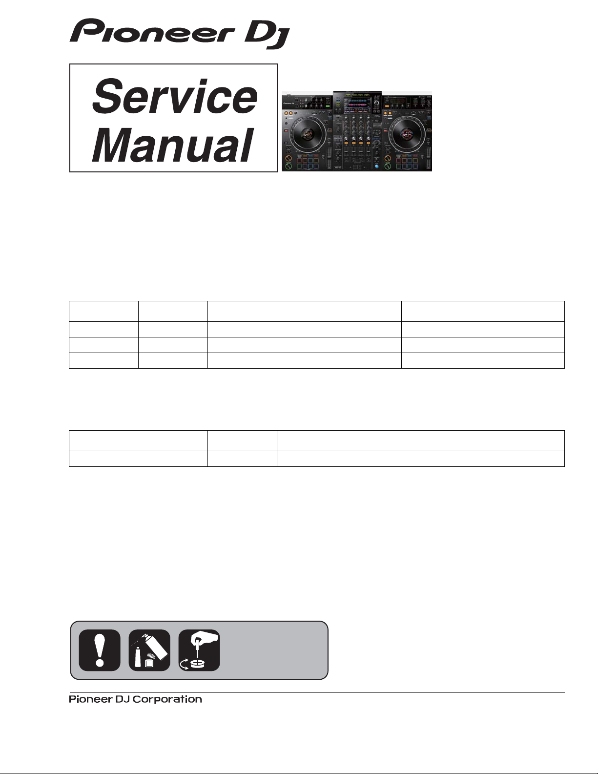
Pioneer XDJ-XZ Service manual
ORDER NO.
RRV4698
XDJ-XZ
All-In-One DJ System
XDJ-XZ
THIS MANUAL IS APPLICABLE TO THE FOLLOWING MODEL(S) AND TYPE(S).
Model Type Power Requirement Remarks
XDJ-XZ AXJ AC 220 V
XDJ-XZ LWSYXJ AC 110 V to 240 V
XDJ-XZ UXJCB AC 120 V
THIS SERVICE MANUAL SHOULD BE USED TOGETHER WITH THE FOLLOWING MANUAL(S).
Model Order No. Remarks
XDJ-XZ RRV4699 SCHEMATIC DIAGRAM, PCB CONNECTION DIAGRAM, PCB PARTS LIST
6F, Yokohama i-Mark Place, 4-4-5 Minatomirai, Nishi-ku, Yokohama, Kanagawa 220-0012 JAPAN
© 2019 Pioneer DJ Corporation
K-ZZZ OCT. 2019
1
Since the fuse may be neutral of the mains supply, disconnect the mains to de-energize the phase conductors.
Caution
2 3 4
SAFETY INFORMATION
A
B
CONTENTS
SAFETY INFORMATION..........................................................................................................................................................2
1. SERVICE PRECAUTIONS ....................................................................................................................................................3
1.1 NOTES ON SOLDERING ...............................................................................................................................................3
1.2 NOTES ON REPLACING................................................................................................................................................3
1.3 SERVICE NOTICE ..........................................................................................................................................................4
2. SPECIFICATIONS .................................................................................................................................................................6
3. BASIC ITEMS FOR SERVICE...............................................................................................................................................7
C
D
E
F
3.1 CHECK POINTS AFTER SERVICING............................................................................................................................7
3.2 JIGS LIST .......................................................................................................................................................................8
3.3 PCB LOCATIONS .........................................................................................................................................................11
4. BLOCK DIAGRAM...............................................................................................................................................................13
4.1 OVERALL WIRING DIAGRAM (1/2) .............................................................................................................................13
4.2 OVERALL WIRING DIAGRAM (2/2) .............................................................................................................................14
4.3 OVERALL BLOCK DIAGRAM.......................................................................................................................................15
4.4 POWER BLOCK DIAGRAM..........................................................................................................................................16
4.5 MATRIX INFORMATION ...............................................................................................................................................17
5. DIAGNOSIS.........................................................................................................................................................................20
5.1 STARTUP SEQUENCE.................................................................................................................................................20
5.2 TROUBLESHOOTING ..................................................................................................................................................21
5.3 SIMPLIFIED DIAGNOSTIC PROCEDURE FOR AUDIO SIGNAL................................................................................34
5.4 VOLTAGE MONITORING CIRCUIT ..............................................................................................................................35
5.5 ERROR DISPLAY .........................................................................................................................................................38
6. SERVICE MODE .................................................................................................................................................................39
6.1 TEST MODE .................................................................................................................................................................39
6.2 LCD CALIBRATION MODE...........................................................................................................................................49
6.3 ABOUT THE DEVICE ...................................................................................................................................................50
7. DISASSEMBLY....................................................................................................................................................................51
8. EACH SETTING AND ADJUSTMENT ................................................................................................................................74
8.1 NECESSARY ITEMS TO BE NOTED...........................................................................................................................74
8.2 UPDATING OF THE FIRMWARE .................................................................................................................................75
8.3 JOG DIAL ROTATION LOAD ADJUSTMENT ...............................................................................................................76
8.4 TEMPO ZERO POINT ADJUSTMENT .........................................................................................................................78
8.5 WRITING THE SERIAL NUMBER OF THE UNIT .......................................................................................
8.6 USER SETABLE ITEMS ...............................................................................................................................................80
9. EXPLODED VIEWS AND PARTS LIST...............................................................................................................................82
9.1 PACKING SECTION .....................................................................................................................................................82
9.2 BOTTOM SECTION......................................................................................................................................................84
9.3 CHASSIS SECTION .....................................................................................................................................................86
9.4 CONTROL PANEL SECTION (1/3)...............................................................................................................................88
9.5 CONTROL PANEL SECTION (2/3)...............................................................................................................................90
9.6 CONTROL PANEL SECTION (3/3)...............................................................................................................................92
9.7 JOG DIAL SECTION.....................................................................................................................................................94
9.8 LCD SECTION..............................................................................................................................................................96
.................79
2
1
2 3 4
XDJ-XZ
5
For environmental protection, lead-free solder is used on the printed circuit boards mounted in this unit.
Be sure to use lead-free solder and a soldering iron that can meet specifications for use with lead-free solders for repairs
accompanied by reworking of soldering.
Do NOT use a soldering iron whose tip temperature cannot be controlled.
The part listed below is difficult to replace as a discrete component part.
When the part listed in the table is defective, replace whole Assy.
Assy Name
MAIN Assy
DC-DC CONVERTER (System power supply)BD9328EFJ IC with heat-pad
IC301
JLCD1 Assy
REGULATOR IC (JOG-LCD UCOM power supply)
BD00IC0WEFJ IC with heat-pad
IC3001
JLCD2 Assy
REGULATOR IC (JOG-LCD UCOM power supply)
BD00IC0WEFJ IC with heat-pad
IC3201
XPAD Assy
Microcontroller (X-PAD control)ATSAMD20E15A-MU QFN IC with heat-pad
IC3401
LCDB Assy
DC-DC CONVERTER (BROWSE-LCD power supply)
R1290K103A QFN IC with heat-pad
IC3605
INTERFACE IC (TOUCH PANEL control)AK4187VN QFN IC with heat-pad
IC3606
AUDIO Assy
Multi DAC IC (MASTER/BOOTH/SEND output)AK4458VN QFN IC with heat-pad
IC5802
TRANSISTOR (HP output)2SCR573D3 Tr with heat-pad
Q6413, Q6415
TRANSISTOR (HP output)2SAR573D3 Tr with heat-pad
Q6414, Q6416
DC-DC CONVERTER (LED power supply)BD9328EFJ IC with heat-pad
IC6602, IC6603
DC-DC CONVERTER (AUDIO power supply)BD9851EFV IC with heat-pad
IC6605, IC6606
REGULATOR IC (AUDIO power supply)NJM78M09DL1A IC with heat-pad
IC6607
REGULATOR IC (AUDIO power supply)NJM7805DL1A IC with heat-pad
IC6609, IC6610
REGULATOR IC (AUDIO power supply)NJM78M15DL1A IC with heat-pad
IC6611
REGULATOR IC (AUDIO power supply)NJM79M15DL1A IC with heat-pad
IC6612
REGULATOR IC (System power supply)BD00IC0WEFJ IC with heat-pad
IC302
DRIVER IC (BROWSE-LCD backlight power supply)
IS31BL3555-ZLS4 IC with heat-pad
IC303
DC-DC CONVERTER (System power supply)BD9328EFJ IC with heat-pad
IC501
PO SUPPLY IC (Power management IC)MMPF0100F0AEP QFN IC with heat-pad
IC502
U-PRO IC (Application processor)MCIMX6Q6AVT10AD BGA
IC701
RAM IC (DDR3)K4B4G1646E-BYMA BGA
IC901, IC902
DC-DC CONVERTER (USB-A power supply)BD9328EFJ IC with heat-pad
IC1801, IC1802
High-side SW IC (USB-A current control)TPS2557DRB IC with heat-pad
IC1803, IC1804
INTERFACE IC (USB-A HUB)TUSB4020BIPHP IC with heat-pad
IC1805
INTERFACE IC (USB-LAN conversion)RTL8152B-VB-CG QFN IC with heat-pad
IC2001
INTERFACE IC (USB-B HUB)TUSB4041IPAP IC with heat-pad
IC2002
INTERFACE IC (LAN HUB)RTL8309M-CG QFN IC with heat-pad
IC2151
DSPD810K013DZKB400 BGA
IC2501
Authentication Coprocessor (MFi authentication)H337S3959 USON package
(UltraSmallOutlineNon-lead)
IC1101
Parts that is Difficult to Replace
Ref No. FunctionPart No. Remarks
6 7 8
1. SERVICE PRECAUTIONS
1.1 NOTES ON SOLDERING
A
1.2 NOTES ON REPLACING
B
C
D
E
XDJ-XZ
5
6 7 8
F
3
1
g About the assembly of the JOG dial display
The JOG panel is not coloring to improve the visibility of the LCD. So, internal dust and dirt on the surface are easy to see.
Therefore, attention is required when replacing the parts inside the JOG dial (especially when replacing TFT LCD (DWX4228)).
If it gets dirty during work, please remove it before working. In addition, the LCD is performed calibration at the mass
production. Therefore, do the same when replacing.
g Voltage monitoring
This unit always monitors for power failure and will shut itself off immediately after an error is detected.
If a power is defect, MASTER REC (WAKE UP) LED on the right Deck is flashing in a cycle of 250 ms (light on 125 ms and
light off 125 ms).
Other LEDs light off, and SW and VR become not working.
Repair the unit according to the diagnostic procedures described in "5.4 VOLTAGE MONITORING CIRCUIT."
g About the ICs in the MAIN Assy
Replacement of the Flash ROM (IC1102) and USB-LAN Conversion (IC2001) in the MAIN Assy are not possible during service,
because writing of the MAC address on the production line is required.
Therefore, the Flash ROM (IC1102) and USB-LAN Conversion (IC2001) are not supplied as a service part.
If the IC is defective, replace the whole MAIN Assy.
After replacing the the MAIN Assy, writing of the serial number of the unit is required.
For details on how to write the serial number, see "8.5 WRITING THE SERIAL NUMBER OF THE UNIT."
g Confirmation of user-setting
This product has user-setting data. Be sure to confirm those data before starting repair, although changing them may not have
a large effect. Use the Check Sheet in "8.6 USER SETABLE ITEMS" to which you can transcribe the settings, as required.
The settings are stored in FLASH ROM (IC1102) on the MAIN Assy.
For details, refer to "Changing the settings" in the operating instructions.
g How to modify when the rattling of the product is occurred
" Place the 13 points (g) of the control panel under the block (Height more than 40 mm and Diameter arround φ20 mm is
recommended), and attach the chassis part according to the screw tightening order manually.
(The block is available at the home center, etc.)(Refer to "7 DISASSEMBLY" about the screw tightening order.)
" When there is no block, place the whole surface of the control panel to the curing mat, and attach the chassis part according
to the screw tightening order manually.
" Take care not to press the screwdriver strongly to the product in any case.
" Do not use the electric screwdriver.
2 3 4
1.3 SERVICE NOTICE
A
B
C
D
E
F
4
1
2 3 4
XDJ-XZ
5
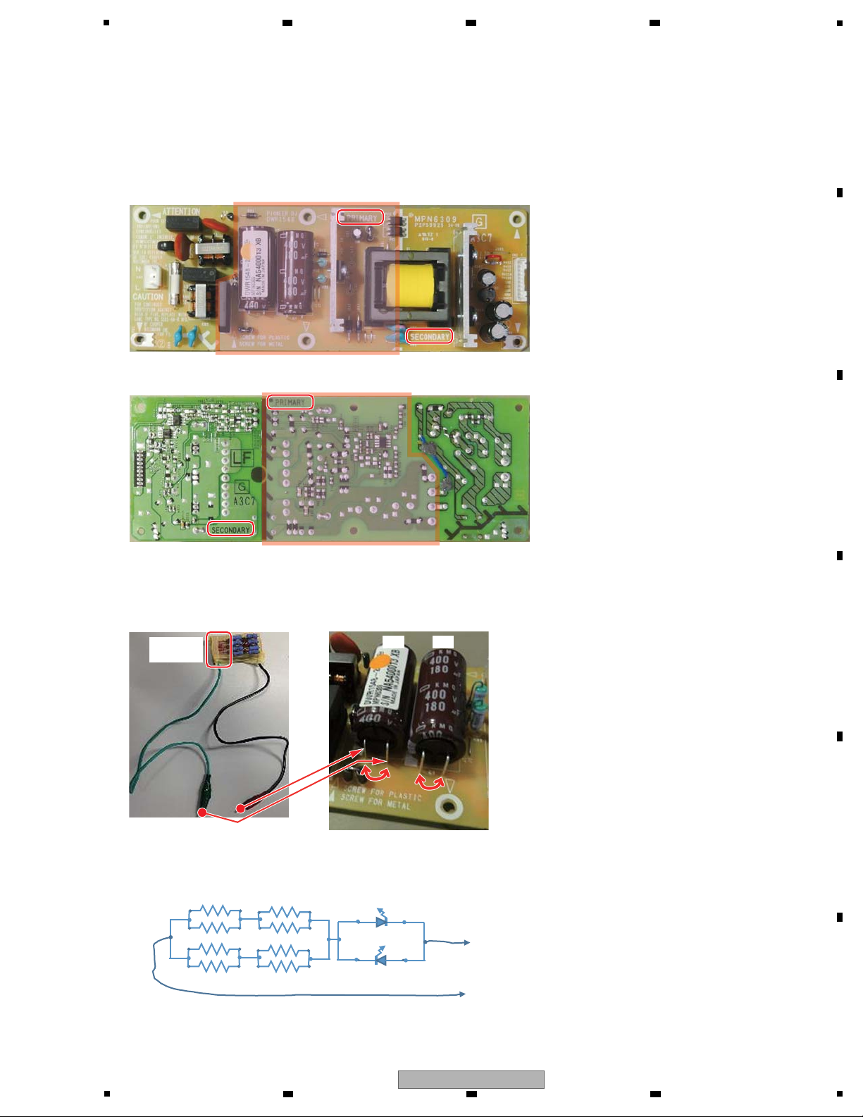
When discharging the above point, use the following discharge jig as needed.
While the charging voltage is left of both C4 and C5, either of checking LEDs turns on.
And if both of LED turns off, we can avoid receiving the electrical shock!!
When there is no above type LED, take measures the following method.
Step 1: After the power is turned off, wait 2 minutes.
Step 2: Connect the Register Jig and leave the unit as it is, for 10 seconds.
! Resister is all 10 kΩ (3W)
! Both of LED is LTL17KRH5D
Checking
LEDs
No
polarity
C4 C5
The circuit of "discharge JIG" is shown below.
g SW POWER SUPPLY Primary side electrical shock
The primary side of SW POWER SUPPLY remains voltage long time, and the primary solder side can be seen.
So if you touch the primary solder side, it is possible to receive an electrical shock.
There is the red area below where we tend to receive an electrical shock.
Be sure to dischsarge the voltage of primary side to avoid receiving the electrical shock.
Electrical shock area of A-side.
Electrical shock area of B-side.
6 7 8
A
B
C
D
E
5
6 7 8
XDJ-XZ
F
5

1
Power requirements ...................... AC 110 V to 240 V, 50 Hz/60 Hz
Power consumption .................................................................55 W
Power consumption (standby) ................................................0.3 W
Main unit weight .................................................... 13.0 kg (28.7 lb)
Max. dimensions
...........................878.0 mm (W) × 466.1 mm (D) × 118.4 mm (H)
(34.6 in. (W) × 18.4 in. (D) × 4.7 in. (H))
Tolerable operating temperature .... +5 °C to +35 °C (+41 °F to +95 °F)
Tolerable operating humidity ...........5 % to 85 % (no condensation)
Audio Section
Sampling rate ....................................................................44.1 kHz
A/D converter ..........................................................................24-bit
D/A converter
MASTER, BOOTH, SEND ................................................. 32-bit
PHONES ...........................................................................24-bit
Frequency characteristic
USB, LINE, AUX (LINE/PORTABLE), MIC ....... 20 Hz to 20 kHz
S/N ratio (rated output, A-WEIGHTED)
USB ................................................................................ 114 dB
LINE ................................................................................ 103 dB
PHONO ............................................................................ 90 dB
AUX (LINE) ....................................................................... 96 dB
AUX (PORTABLE) ............................................................ 90 dB
MIC ................................................................................... 81 dB
Total harmonic distortion (20 Hz to 20 kHzBW)
USB ...............................................................................0.003 %
LINE ...............................................................................0.005 %
PHONO .........................................................................0.017 %
Standard input level / Input impedance
LINE ................................................................... –12 dBu/47 kΩ
PHONO ............................................................. –52 dBu/47 kΩ
AUX (LINE) ........................................................ –12 dBu/47 kΩ
AUX (PORTABLE) ............................................. –24 dBu/47 kΩ
MIC ...................................................................... –57 dBu/3 kΩ
Standard output level / Load impedance / Output impedance
MASTER 1 ..................................... +6 dBu/10 kΩ/390 Ω or less
MASTER 2 ....................................... +2 dBu/10 kΩ/1 kΩ or less
BOOTH .......................................... +6 dBu/10 kΩ/470 Ω or less
SEND ........................................... –12 dBu/10 kΩ/680 Ω or less
PHONES ............................................. +8 dBu/32 Ω/2 Ω or less
Rated output level / Load impedance
MASTER 1 ......................................................... +24 dBu/10 kΩ
MASTER 2 ......................................................... +20 dBu/10 kΩ
BOOTH .............................................................. +24 dBu/10 kΩ
SEND ................................................................. +11 dBu/10 kΩ
Crosstalk
LINE .................................................................................. 97 dB
PHONO ............................................................................ 80 dB
Channel equalizer characteristic
HI ...................................................... –26 dB to +6 dB (20 kHz)
MID ..................................................... –26 dB to +6 dB (1 kHz)
LOW ..................................................... –26 dB to +6 dB (20 Hz)
Microphone equalizer characteristic
HI .................................................... –12 dB to +12 dB (10 kHz)
MID ................................................ –12 dB to +12 dB (2.5 kHz)
LOW ................................................ –12 dB to +12 dB (100 Hz)
MASTER equalizer characteristic
HI ...................................................... –26 dB to +6 dB (20 kHz)
MID ..................................................... –26 dB to +6 dB (1 kHz)
LOW ................................................... –26 dB to + 6 dB (20 Hz)
Input / Output terminals
PHONO input terminals
RCA pin jacks .................................................................. 2 sets
LINE input terminal
RCA pin jacks .................................................................. 2 sets
MIC input terminal
XLR connector & 1/4” TRS jack ....................................... 2 sets
AUX input terminal
RCA pin jacks .................................................................... 1 set
MASTER1 output terminal
XLR connector ................................................................... 1 set
MASTER2 output terminal
RCA pin jacks .................................................................... 1 set
BOOTH output terminal
1/4” TRS jack ..................................................................... 1 set
SEND output terminal
1/4” TS jack ........................................................................ 1 set
PHONES output terminal
1/4” stereo phone jack ....................................................... 1 set
3.5 mm stereo mini jack...................................................... 1 set
USB ports
A type .............................................................................. 2 sets
Power supply ................................................................. 5 V/1 A
B type ................................................................................ 1 set
LINK teminals
LAN teminals (100Base-TX) ............................................ 3 sets
— The specifications and design of this product are subject to
change without notice.
• Power cord
(AXJ: DDG1114)
(LWSYXJ: ADG1244)
(UXJCB: DDG1108)
• USB cable
(DDE1150)
• Operating Instructions (Quick Start Guide)
(AXJ: DRH1542)
(LWSYXJ: DRH1540, DRH1541)
(UXJCB: DRH1539)
• Warranty (LWSYXJ only)
• Software license notice
(AXJ: DRH1594)
(LWSYXJ, UXJCB: DRH1592, DRH1593)
• rekordbox dj license key card
Accessories
2. SPECIFICATIONS
A
2 3 4
B
C
D
E
F
6
1
2 3 4
XDJ-XZ
5
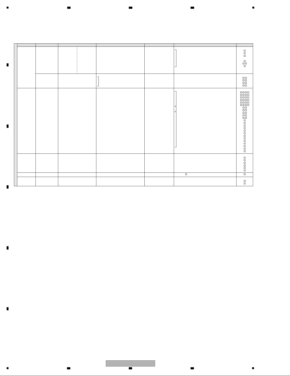
Items to be checked after servicing
No. Procedure Check points
To keep the product quality after servicing, confirm recommended check points shown below.
1 Confirm the firmware version in Test mode.
Distortion
Noise
Volume too low
Volume too high
Volume fluctuating
Sound interrupted
See the table below for the items to be checked regarding audio.
Item to be checked regarding audio
1 The version of the firmware must be latest.
Update firmware to the latest one, if it is not the latest.
2 Confirm whether the customer complaint has been solved.
If the customer complain occurs with the specific source, such as
Mic, each Input, Fader, Equalizer, and Trim, input that specific
source for checking.
The customer complain must not be reappeared.
Audio and operations must be normal.
3 Check the analog audio input (each channel, AUX, MIC1, MIC2).
(Make the analog connections with CDJ player, analog player and
MIC.)
Audio and operations must be normal.
6 Check the LCD display. Check that there is no dirt or dust trapped inside the LCD display.
7 Check the LEDs. Check that all the LEDs light in Test mode.
8 Check operations of the operating elements.
(KEY, SW, VR, Fader, PAD and X-PAD etc.)
Make sure that all buttons and controls on the main unit function
properly in
Test mode.
9 Check the touch panel. Check operation with all black screen in Test mode.
Operations must be normal.
4 Check the analog audio output (MASTER1, MASTER2, BOOTH,
SEND).
Audio and operations must be normal.
5 Check the headphones output.
(1/4” stereo phone plugs and 3.5 mm stereo mini plugs)
There must be no errors, such as noise, in the audio output.
Audio, Search and operations must be normal.
The PC must be linked. The rekordbox software must be linked.
11 Confirm user setting contents. Being repaired to the contents before repairing.
12
Check the appearance of the product.
No scratches or dirt on its appearance after receiving it for service.
10 Check the connection of each interface.
Playback data contained in the device connected to USB A.
Confirm the connection with PC with USB B.
This product is recognized definitely by CDJ player, and LINK be
established.
This product is recognized to a PC definitely, and LINK be
established in rekordbox.
Confirm the connection with CDJ player and the PC by LAN.
6 7 8
3. BASIC ITEMS FOR SERVICE
3.1 CHECK POINTS AFTER SERVICING
A
B
C
D
5
XDJ-XZ
6 7 8
E
F
7
1
Name Part No. Remarks
Jig Name Part No. Purpose of use / Remarks
Lubricants and Glues List
Lubricating oil GEM1106 Used for "9.7 JOG DIAL SECTION".
Refer to "7. DISASSEMBLY".
(Dry surf HFD-1610)
Lubricating oil GYA1001 Used for "9.4 CONTROL PANEL SECTION (1/3)",
"9.5 CONTROL PANEL SECTION (2/3)" and
"9.7 JOG DIALSECTION".
Refer to "7. DISASSEMBLY".
Jigs List
Software for writing the serial
number
GGS1784 For writing the serial number of the unit to the MAIN Assy
after replacement. The file is uploaded to Niis.
Refer to "8.5 WRITING THE SERIAL NUMBER OF THE UNIT."
License-key card for Service GGP1522 For activation of rekordbox dj
License-key card for Service GGP1524 For activation of rekordbox Video
Extension jig FFC (27 pin, L = 500 mm) GGD1903
Used for "8.3 JOG DIAL ROTATION LOAD ADJUSTMENT MODE".
Refer to "7. DISASSEMBLY".
Acetate cloth tape GYH1035 Refer to "9.8 LCD SECTION".
Double side tape GYH1038 NITTO No. 500 (width:10 mm)
Refer to "7. DISASSEMBLY".
(JOG dial Section_Notes for Reassembling TFT LCD)
2 3 4
3.2 JIGS LIST
A
B
C
D
E
F
8
1
2 3 4
XDJ-XZ
5
g XDJ-XZ Service check sheet
1/2
Service Mode
Check contents Check target Operation part, Setting Display part (LED) Display part (LCD) CheckStatus
Version display Firmware etc.
———— ————
PLAY /PAUSE (green)
CUE (orange)
DIRECTION, REV (red)
SLIP (red)
LOOP IN/CUE (IN ADJUST) (orange)
LOOP OUT (OUT ADJUST) (orange)
Jog ring illumination
DIRECTION, REV (red)
SLIP (red)
LOOP IN/CUE (IN ADJUST)
LOOP IN (orange)
LOOP OUT (orange)
RELOOP/EXIT (orange)
LOOP IN/CUE (IN ADJUST) (orange)
LOOP OUT (OUT ADJUST) (orange)
RELOOP/EXIT (orange)
Jog ring illumination
SYNC (INST. DOUBLES) (white)
JOG MODE (VINYL) (blue)
Jog ring illumination (white)
LOOP OUT (OUT ADJUST) (orange)
LOOP IN/CUE (IN ADJUST) (orange)
SYNC MASTER (orange)
MASTER TEMPO (red)
MASTER (orange)
HOT CUE (CALL)
BEAT LOOP
SLIP LOOP
BEAT JUMP
PAD-1
PAD-2
PAD-3
PAD-4
PAD-5
PAD-6
PAD-7
PAD-8
VERSION INFORMATION
SYSTEM
EUP
PANEL M
JOG LCD(DECK1)
JOG LCD(DECK2)
LANGUAGE
MAC_ADDR
MAC_ADDR(LAN)
SERIAL
UPDATE PORT
OPERATION CHECK
g Ver.
g Ver.
g Ver.
g Ver.
g Ver.
g
g
g
g
g
g
g
g
g/g
g/g
g/g
g/g
g/g
g/g
g/g
g/g
g/g
g/g
g/g
g/g
g/g
g/g
g/g
g/g
g/g
g/g
g/g
g/g
g/g
g/g
g/g
g/g
g/g
g/g
g/g
g/g
g/g
g/g
g/g
g/g
g/g
g/g
g/g
g/g
g/g
Firmware version display
These LED light on dimly
Language selection display
Serial number display
Update port check display
Mode 5 to 10 operation complete check display
All LEDs and
LCDs light on
All LED, LCD Rotary selector All LED, LCD DISPLAY ON ————
gLCD patterns LCD Rotary selector ———— LCD PATTERN TEST Cyclic pressed: color l black l white
Cyclic pressed: red l green l blue l white l OFF
All LEDs and
LCDs light off
(or light on dimly)
All LED, LCD Rotary selector All LED, LCD
rekordbox (white)
LINK (blue)
USB1 (green)
USB2 (green)
BROWSE (green)
TAG LIST (green)
INFO (green)
MENU (green)
DISPLAY OFF Turn to the right once it l light off
Individual keys
and LEDs
Button DECK 1 / 2
f (PLAY /PAUSE)
CUE
SEARCH (m)
SEARCH (n)
TRACK SEARCH (o)
TRACK SEARCH (p)
SHIFT
DIRECTION, REV
SLIP
4/8 BEAT (LOOP CUTTER)
LOOP IN/CUE (IN ADJUST)
LOOP OUT (OUT ADJUST)
RELOOP/EXIT
CUE/LOOP CALL c (LOOP 1/2X)
CUE/LOOP CALL d (LOOP 2X)
DELETE
MEMORY
SYNC (INST. DOUBLES)
JOG MODE (VINYL)
JOG (TOUCH)
JOG ROTATE FWD
JOG ROTATE REV
TEMPO
MASTER TEMPO
SYNC MASTER
HOT CUE (CALL)
BEAT LOOP
SLIP LOOP
BEAT JUMP
PAD-1
PAD-2
PAD-3
PAD-4
PAD-5
PAD-6
PAD-7
PAD-8
KEY/LED TEST
CH1 / CH2 PLAY/PAUSE
CH1 / CH2 CUE
CH1 / CH2 SEARCH REV
CH1 / CH2 SEARCH FWD
CH1 / CH2 TRACK REV
CH1 / CH2 TRACK FWD
CH1 / CH2 SHIFT
CH1 / CH2 REVERSE
CH1 / CH2 SLIP
CH1 / CH2 4 BEAT
CH1 / CH2 LOOP IN
CH1 / CH2 LOOP OUT
CH1 / CH2 RELOOP
CH1 / CH2 CALL PREV
CH1 / CH2 CALL NEXT
CH1 / CH2 CUE DELETE
CH1 / CH2 CUE MEMORY
CH1 / CH2 SYNC
CH1 / CH2 VINYL
CH1 / CH2 JOG TOUCH
CH1 / CH2 JOG ROTATE FWD
CH1 / CH2 JOG ROTATE REV
CH1 / CH2 TEMPO RANGE
CH1 / CH2 MASTER TEMPO
CH1 / CH2 MASTER
CH1 / CH2 HOT CUE
CH1 / CH2 AUTO BEAT LOOP
CH1 / CH2 SLIP LOOP
CH1 / CH2 BEAT JUMP
CH1 / CH2 PAD1
CH1 / CH2 PAD2
CH1 / CH2 PAD3
CH1 / CH2 PAD4
CH1 / CH2 PAD5
CH1 / CH2 PAD6
CH1 / CH2 PAD7
CH1 / CH2 PAD8
Press l light on, release l light off
Press l light on, release l light off
Cyclic pressed: red l green l blue l white l OFF
REKORDBOX (white)
LINK (blue)
USB1 (green)
USB2 (green)
BROWSE (SEARCH) (green)
TAGLIST (green)
INFO (green)
MENU (UTILITY) (green)
DECK QUANTIZE (red)
DECK QUANTIZE (red)
ROTARY SELECTOR (white)
BROWSE (SEARCH) (green)
TAGLIST (green)
INFO (green)
MENU (UTILITY) (green)
LOAD1 (white)
LOAD2 (white)
USB1 (white)
USB2 (white)
MASTER REC (WAKE UP)(red)
MASTER REC (WAKE UP)(white)
g
g
g
g
g
g
g
g
g
g
g
g
g
g
g
g
g
g
g
g
g
Common
REKORDBOX
LINK
USB1
USB2
BROWSE (SEARCH)
TAGLIST
INFO
MENU (UTILITY)
DECK QUANTIZE
TIME
ROTARY SELECTOR
BACK
TAG TRACK/REMOVE
TRACK FILTER (EDIT)
SHORT CUT
LOAD1
LOAD2
USB1 STOP
USB2 STOP
MASTER REC (WAKE UP)
TRACK MARK
MEDIA RB
MEDIA LINK
MEDIA USB1
MEDIA USB2
BROWSE
TAGLIST
INFO
MENU
DECK QUANTIZE
TIME MODE/ACUE
ROTARY SELECTOR
BACK
TAG TRACK
TRACK FILTER
SHORT CUT
CH1 LOAD
CH2 LOAD
CH1 USB STOP
CH2 USB STOP
USB REC
TRACK MARK
Press l light on, release l light on dimly
Press l light on, release l light on dimly
Press l light on, release l light off
Press l light on, release l light off
SOUND COLOR FX SWEEP (white)
SOUND COLOR FX DUB ECHO (white)
SOUND COLOR FX SPACE (white)
SOUND COLOR FX NOISE (white)
SOUND COLOR FX CRUSH (white)
SOUND COLOR FX FILTER (white)
CUE CH1 (orange)
CUE CH2 (orange)
CUE CH3 (orange)
CUE CH4 (orange)
CUE MASTER (orange)
BEAT FX ON/OFF (blue)
FX FREQUENCY HI (blue)
FX FREQUENCY MID (blue)
FX FREQUENCY LOW (blue)
FX QUANTIZE (red)
TAP (green)
FX QUANTIZE (red)
TAP (green)
BEAT FX ON/OFF (white)
MIC TALK OVER (red)
FEEDBACK REDUCER (green)
g
g
g
g
g
g
g
g
g
g
g
g
g
g
g
g
g
g
g
g
g
g
Mixer
SOUND COLOR FX SWEEP
SOUND COLOR FX DUB ECHO
SOUND COLOR FX SPACE
SOUND COLOR FX NOISE
SOUND COLOR FX CRUSH
SOUND COLOR FX FILTER
CUE CH1
CUE CH2
CUE CH3
CUE CH4
CUE MASTER
BEAT FX ON/OFF
FX FREQUENCY HI
FX FREQUENCY MID
FX FREQUENCY LOW
AUTO/TAP
TAP
FX QUANTIZE
BEAT (d)
BEAT (c)
MIC TALK OVER
FEEDBACK REDUCER
CFX SWEEP
CFX DUB ECHO
CFX SPACE
CFX NOISE
CFX CRUSH
CFX FILTER
CH1 HEADPHONE CUE CH
CH2 HEADPHONE CUE CH
CH3 HEADPHONE CUE CH
CH4 HEADPHONE CUE CH
MASTER CUE
EFFECT ON/OFF
FX HI
FX MID
FX LOW
AUTO/TAP
TAP
FX QUANTIZE
BEAT NEXT
BEAT PREV
TALKOVER
FEEDBACK REDUCER
Press l light on, release l light off
6 7 8
A
B
C
D
E
F
XDJ-XZ
5
6 7 8
9
1
2/2
Service Mode
g
g
g
g
g/g
g
g/g/g/g
g/g/g/g
g/g/g/g
g/g/g/g
g/g/g/g
g/g/g/g
g/g
g/g
g/g
g/g
g/g
g
g
g
g
g
g
g
g
g
g
g
g
g
Individual switches,
MIC LEDs
and PAD LEDs
INPUT SELECT(CH3)
INPUT SELECT(CH4)
CROSS FADER ASSIGN
(CH1/CH2/CH3/CH4)
AUX
MIC1 / MIC2
FEEDBACK REDUCER
PC / LINE / PHONO
PC / LINE / PHONO
A / THRU / B
OFF / LINE / PORTABLE
OFF / ON
LIGHT / HEAVY
Display on LCD when selected
SW select
MIC 1/2 (OFF: light off, ON: light on)
MIC 1/2 CLIP, MIC 1/2 SIGNAL
(LIGHT d CLIP light on, SIGNAL: light off
HEAVY d CLIP: light off, SIGNAL: light on)
SW TEST
PC / LINE / PHONO
PC / LINE / PHONO
A / THRU / B
OFF / LINE / PORTABLE
OFF / ON
LIGHT / HEAVY
Values of the rotary
variable controls
and sliders
X-PAD test
CH1 / CH2 / CH3 / CH4 TRIM
CH1 / CH2 / CH3 / CH4 HI
CH1 / CH2 / CH3 / CH4 MID
CH1 / CH2 / CH3 / CH4 LOW
CH1 / CH2 / CH3 / CH4 COLOR
CH1 / CH2 / CH3 / CH4 FADER
CH1 / CH2 TEMPO
CH1 / CH2 TOUCH/RELESE
MIC1 / MIC2 EQ HI
MIC1 / MIC2 EQ MIDI
MIC1 / MIC2 EQ LOW
HP MIXING
HP LEVEL
EFFECT PARAMETER
AUX TRIM
CROSS FADER
LEVEL/DEPTH
BOOTH LEVEL
MASTER LEVEL
MASTER EQ HI
MASTER EQ MIDI
MASTER EQ LOW
BEAT EFFECT SELECTOR
BEAT CH SELECTOR
Display the value (000 to 3FF hexadecimal)
to the position of VR.
Display the value (000 to 3FF hexadecimal)
to the position of VR.
Display the value (000 to 00D hexadecimal) to the position of switch.
Display the value (000 to 00A hexadecimal) to the position of switch.
Display the value (000 to 3FF0 hexadecimal)
to the position of VR.
VOL TEST
CH1 / CH2 / CH3 / CH4 TRIM xxx
CH1 / CH2 / CH3 / CH4 HI xxx
CH1 / CH2 / CH3 / CH4 MID xxx
CH1 / CH2 / CH3 / CH4 LOW xxx
CH1 / CH2 / CH3 / CH4 COLOR xxx
CH1 / CH2 / CH3 / CH4 FADER xxx
CH1 / CH2 TEMPO xxx
CH1 / CH2 TOUCH/RELESE xxx
MIC1 / MIC2 EQ HI xxx
MIC1 / MIC2 EQ MIDI xxx
MIC1 / MIC2 EQ LOW xxx
HP MIXING xxx
HP LEVEL xxx
PARAMETER xxx
AUX TRIM xxx
CROSS FADER xxx
LEVEL DEPTH xxx
BOOTH LEVEL xxx
MASTER LEVEL xxx
MASTER EQ HI xxx
MASTER EQ MIDI xxx
MASTER EQ LOW xxx
BEAT FX TYPE xxx
BEAT FX CH xxx
————
Volume operation
g
g
g
g
g
g
X-PAD upper
X-PAD lower
X-PAD upper
X-PAD lower
X-PAD SLICER
X-PAD POSITION
Touch l ON, Release l OFF
Touch l ON, Release l OFF
Display the value (00 to FF hexadecimal) to the touch position of upper
Display the value (00 to FF hexadecimal) to the touch position of lower
Display the value (00 to FF hexadecimal) to the touch position of slicer
Display the beat information
to the touch position
X-PAD TEST
TOUCH UPPER ON / OFF
TOUCH LOWER ON / OFF
X-PAD UPPER xxx
X-PAD LOWER xxx
X-PAD SLICER xxx
TOUCH POSITION xxx
————
X-PAD operation
Touch panel test g———— Touch four g position l green, display "Touch test OK"TOUCH PANEL TEST————
Touch operation
Rotary selector
g
g
ROTARY SELECTOR
TIME
Display the value (00 to FF hexadecimal) to the position of selector.
Display the value (00 to FF hexadecimal) to the position of selector.
SELECTOR TEST
SELECTOR xx
TIME xx
————
Select operation
g/g
g/g
g/g
g/g
DECK 1 / 2
PAD MODE (HOT CUE (CALL))
PAD MODE (BEAT LOOP)
PAD MODE (SLIP LOOP)
PAD MODE (BEAT JUMP)
Press l light on red
Press l light on green
Press l light on blue
Press l light on white
PAD LED(lump)
Performance Pads ×8,
PAD MODE buttons ×4
————
Check contents Check target Operation part, Setting Display part (LED) Display part (LCD) CheckStatus
2 3 4
A
B
C
D
E
F
10
XDJ-XZ
1
2 3 4
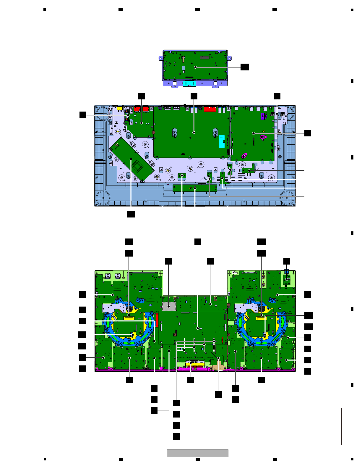
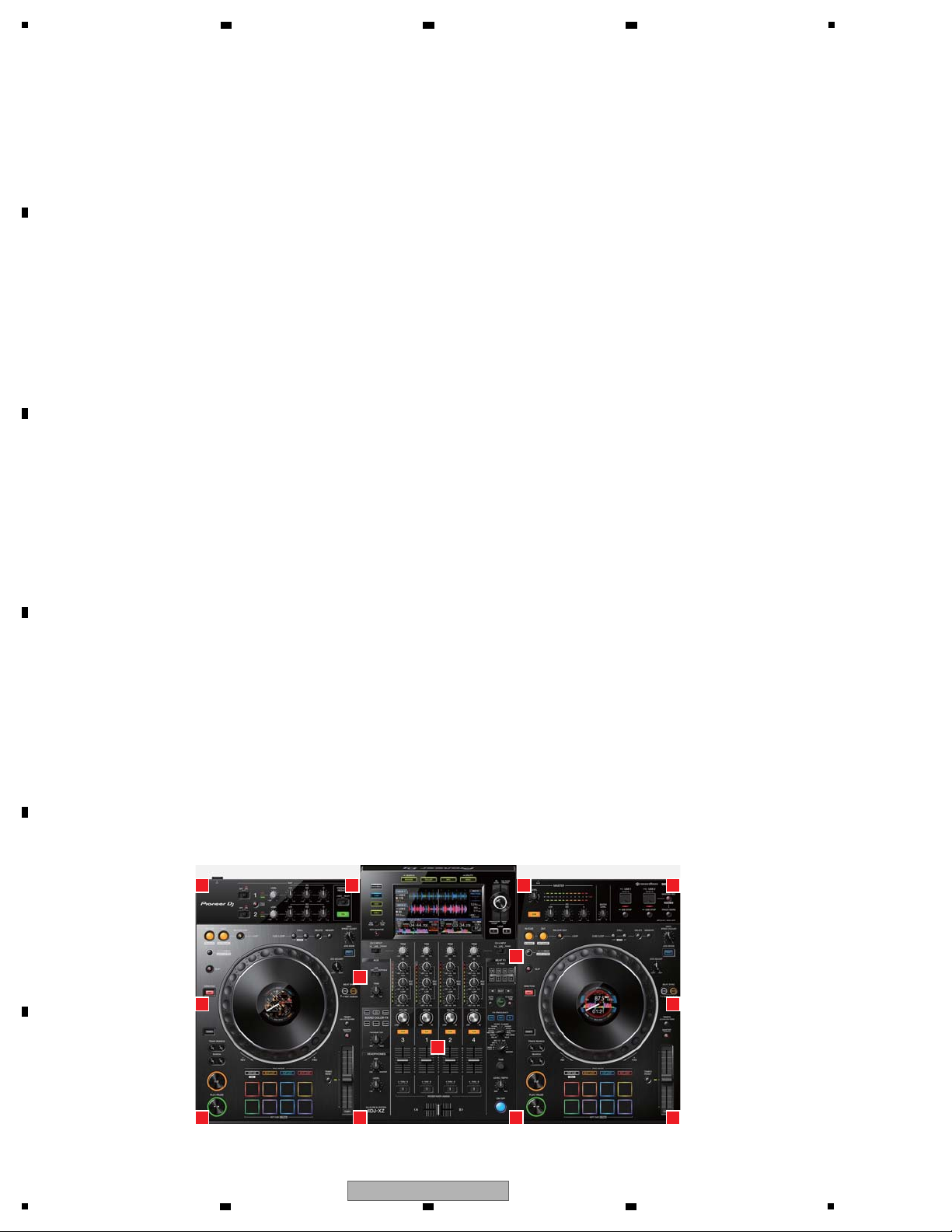
3.3 PCB LOCATIONS
Note:
The 1 and 2 Assys of JLCD, PLAY, SER, TMP and JOG Assys have the same circuitry, parts, and board shapes.
Only printed information is different, because their part numbers and wiring numbers are different.
They are handled similarly in their production management.
Therefore, either 1 or 2 Assy of the respective Assys is assembled in the respective place.
The 1 to 4 Assys of CHF Assys have the same circuitry, parts, and board shapes.
Only printed information is different, because their part numbers and wiring numbers are different.
They are handled similarly in their production management.
Therefore, either 1, 2, 3 or 4 Assy of the respective Assys is assembled in the respective place.
" Bottom view
" Bottom view
" Chassis Section
B
AE
LCDB ASSY
AUDIO ASSY
C
MCIN ASSY
D
MCTR ASSY
E
USBA ASSY
S
PWSW ASSY
O
PAD1 ASSY
P
PAD2 ASSY
F
HPJK ASSY
N
CRFD
ASSY
H
MIXER ASSY
G
UCOM ASSY
A
MAIN ASSY
R
DCK1 ASSY
JLCD1 ASSY
Z
PLAY2 ASSY
or
Y
PLAY1 ASSY
Z
PLAY2 ASSY
or
Y
PLAY1 ASSY
X
SER2 ASSY
or
or
W
SER1 ASSY
V
TMP2 ASSY
or
U
TMP1 ASSY
T
DCK2 ASSY
" Control Panel Section
AF
SW POWER SUPPLY STL1 ASSY STL4 ASSY
STL2 ASSY
STL3 ASSY
STL2 ASSY
STL3 ASSY
AA
JLCD2 ASSY
AB
JOG1 ASSY
or
AC
JOG2 ASSY
AD
JOG1 ASSY
or
AC
JOG2 ASSY
AD
JLCD1 ASSY
or
AA
JLCD2 ASSY
AB
V
TMP2 ASSY
or
U
TMP1 ASSY
X
SER2 ASSY
or
W
SER1 ASSY
Q
XPAD ASSY
K
CHF2 ASSY
or
L
CHF3 ASSY
or
M
CHF4 ASSY
or
J
CHF1 ASSY
I
EFSW ASSY
5
6 7 8
A
B
C
D
5
6 7 8
XDJ-XZ
E
F
11

1
Mark No. Description Part No. Mark No. Description Part No.
LIST OF ASSEMBLIES
NOTES: - Parts marked by “NSP” are generally unavailable because they are not in our Master Spare Parts List.
-
The > mark found on some component parts indicates the importance of the safety factor of the part.
Therefore, when replacing, be sure to use parts of identical designation.
1..MAIN ASSY DWX4287
NSP 1..PADA ASSY DWM2720
2..LCDB ASSY DWX4291
2..PAD1 ASSY DWX4292
2..PAD2 ASSY DWX4293
2..USBA ASSY DWX4294
2..CRFD ASSY DWX4295
NSP 1..JOGA ASSY DWM2719
2..JLCD1 ASSY DWX4288
2..JLCD2 ASSY DWX4289
2..XPAD ASSY DWX4290
1..AUDIO ASSY DWX4298
NSP 1..SUBA ASSY DWM2724
2..MCIN ASSY DWX4300
2..HPJK ASSY DWX4301
2..MCTR ASSY DWX4302
2..CHF1 ASSY DWX4303
2..CHF2 ASSY DWX4304
2..PLAY1 ASSY DWX4307
2..PLAY2 ASSY DWX4308
2..SER1 ASSY DWX4310
2..SER2 ASSY DWX4314
NSP 1..UCOMA ASSY DWM2721
2..UCOM ASSY DWX4296
2..EFSW ASSY DWX4297
1..MIXER ASSY DWX4299
NSP 1..PNL1 ASSY DWM2725
2..DCK1 ASSY DWX4309
2..TMP1 ASSY DWX4311
2..PWSW ASSY DWX4312
2..CHF3 ASSY DWX4305
2..STL1 ASSY DWX4319
2..STL2 ASSY DWX4320
2..STL3 ASSY DWX4321
NSP 1..PNL2 ASSY DWM2726
2..DCK2 ASSY DWX4313
2..TMP2 ASSY DWX4315
2..CHF4 ASSY DWX4306
2..JOG1 ASSY DWX4317
2..JOG2 ASSY DWX4318
2..STL4 ASSY DWX4322
> 1..SW POWER SUPPLY DWR1548
A
2 3 4
B
C
D
E
F
12
1
2 3 4
XDJ-XZ
AKM1289
CN4401
1
V+3R3D2_AD_SH
2
FADER_AD
3
GNDD_AD_SH
CN3006
CKS6646
1
LED-2LED-3LED-4LED+5GND6NC7NC8NC9NC
10
GND
11
NC12NC13NC
14
RESET15CS
16
SCL17SDI
18NC19
NC
20
DATA021DATA122DATA223DATA324DATA4
25
DATA5
26NC27
NC
28
DATA629DATA7
30
DATA831DATA932DATA1033DATA1134NC35NC
36
DATA1237DATA1338DATA1439DATA1540DATA1641DATA17
42
HSYNC43VSYNC
44
DOTCLK
45NC46
NC47VCI48VCI49NC
50
NC
51
NC
52
NC53NC
54
NC
55
NC
56
NC
57
NC
58
ENABLE59GND60GND
CN3206
CKS6646
1
LED-2LED-
3
LED-
4
LED+5GND6NC7NC8NC9NC10GND11NC12NC13NC14RESET
15CS16
SCL17SDI18NC19NC
20
DATA0
21
DATA122DATA2
23
DATA3
24
DATA4
25
DATA526NC27NC28DATA6
29
DATA730DATA8
31
DATA9
32
DATA1033DATA1134NC
35NC36
DATA1237DATA1338DATA14
39
DATA15
4
0
DATA1641DATA1742HSYNC
43
VSYNC44DOTCLK45NC46NC47VCI48VCI49NC
50NC51
NC52NC53NC54NC55NC
56NC57NC58
ENABLE59GND60GND
CN3003
CKS1072
1
JOG_SW
2
NC
3
GNDD
CN4511
KM200NA3
1
GNDD_AD_SH2FADER_AD3V+3R3D2_AD_SH
CN4510
KM200NA3
1
GNDD_AD_SH
2
FADER_AD3V+3R3D2_AD_SH
CN4514
KM200NA3
1
V+3R3D2_AD_SH2FADER_AD
3
GNDD_AD_SH
CN4513
KM200NA3
1
GNDD_AD_SH2FADER_AD3V+3R3D2_AD_SH
CN4512
KM200NA3
1
GNDD_AD_SH2FADER_AD3V+3R3D2_AD_SH
CKS6645
CN4508
1
GNDD
2
GNDD3V+5E4V+5E5GNDD6MAS_VR_MUTE7GNDD8ERP_xAMUTE9GNDD10FAULT_DET
11
GNDD12PWR_ON13GNDD14GNDD
15
GNDD16V+12BL17V+12BL
18
GNDD_LED19GNDD_LED20V+9LED
21
V+9LED22V+9LED23GNDD_LED24GNDD_LED
25
GNDD_LED
26
GNDD_LED27GNDD_LED28GNDD_LED
29
V+5LED30V+5LED31V+5LED32GNDD33GNDD34V+3R3D2_AD_SH35V+3R3D2_AD_SH
36
GNDD_AD_SH37CROSS_FADER38GNDD_AD_SH39CH3_FADER40GNDD_AD_SH
41
CH1_FADER42GNDD_AD_SH43CH2_FADER44GNDD_AD_SH45CH4_FADER
46
GNDD_AD_SH47GNDD_AD_SH48GNDD
49
GNDD50GNDD
CKS6645
CN4505
1
GNDD2xRDY23GNDD4GNDD
5
GNDD6JU2_SCLK7GNDD
8
JU2_MISO9GNDD10JU2_MOSI11GNDD12ERP_IMX_POR13GNDD
14
ERP_xCS15ERP_WRITE16GNDD17ERP_MISO18GNDD19ERP_MOSI
20
GNDD21ERP_SCLK
22
GNDD23ERP_REQ24ERP_CONT25PNL_REQ26GNDD27PNL_xCS1
28
PNL_xCS2
29
PNL_CONT30GNDD31PNL_MISO32GNDD33PNL_MOSI34GNDD35PNL_SCLK
36
GNDD37xRDY138GNDD39GNDD40GNDD41JU1_SCLK42GNDD43JU1_MISO44GNDD45JU1_MOSI46GNDD
47
V+3R3D2
48
V+3R3D249V+3R3D2
50
GNDD
DKP3953
CN4516
1
V+9LED_O
2
V+9LED_O
3
V+9LED_O
4
GNDD_LED
5
GNDD_LED
6
GNDD_LED7GNDD8PADGRID1
9
GNDD10PADGRID0
11
GNDD12PADGRID213GNDD14PAD1_B8
15
PAD1_B716PAD1_B617PAD1_B5
18
GNDD
19
PAD1_B120PAD1_B221PAD1_B322PAD1_B4
23
V+3R3D224V+3R3D2
25
GNDD
26
PAD1_SI0
27
GNDD28PAD_xG
29
GNDD30PAD_RCK
31
GNDD
32
PAD1_SCLK0
33
GNDD
34
PAD1_SI135GNDD
36
PAD1_SCLK137GNDD
38
GNDD_AD_DCK39GNDD_AD_DCK
40
PAD1MODE_AD41PAD1_142PAD1_243PAD1_3
44
PAD1_445PAD1_8
46
PAD1_747PAD1_6
48
PAD1_5
49
V+3R3D2_AD_DCK
50
V+3R3D2_AD_DCK
CKS6645
CN4504
1
V+3R3D2_AD_DCK
2
V+3R3D2_AD_DCK3PAD2_84PAD2_75PAD2_66PAD2_5
7
PAD2_1
8
PAD2_2
9
PAD2_310PAD2_4
11
PAD2MODE_AD12GNDD_AD_DCK13GNDD_AD_DCK14GNDD
15
PAD2_SI0
16
GNDD
17
PAD2_SCLK0
18
GNDD
19
PAD2_SI120GNDD21PAD_xG22GNDD
23
PAD_RCK24GNDD
25
PAD2_SCLK126GNDD27V+3R3D228V+3R3D229PAD2_B130PAD2_B2
31
PAD2_B332PAD2_B4
33
GNDD
34
PAD2_B8
35
PAD2_B736PAD2_B637PAD2_B5
38
GNDD39PADGRID2
40
GNDD
41
PADGRID042GNDD43PADGRID144GNDD45GNDD_LED
46
GNDD_LED
47
GNDD_LED
48
V+9LED_O49V+9LED_O50V+9LED_O
VKN1287
CN4503
1
GNDD
2
V+12BL_O
3
GNDD_LED
4
GNDD_LED
5
V+9LED_O
6
V+9LED_O
7
GNDD
8
GNDD
9
V+3R3D2_J
10
V+3R3D2_J
11
GNDD
12
ERP_WRITE
13
GNDD
14
GNDD
15
LR_DET2_L
16
GNDD
17
xRDY2
18
GNDD
19
JU2_MOSI
20
GNDD
21
JU2_MISO
22
GNDD
23
JU2_SCLK
24
GNDD
25
SUBU_RST
26
GNDD
27
GNDD
VKN1287
CN4515
1
GNDD
2
GNDD
3
SUBU_RST
4
GNDD
5
JU1_SCLK
6
GNDD
7
JU1_MISO
8
GNDD
9
JU1_MOSI
10
GNDD
11
xRDY1
12
GNDD
13
LR_DET1_H
14
GNDD
15
GNDD
16
ERP_WRITE
17
GNDD
18
V+3R3D2_J
19
V+3R3D2_J
20
GNDD
21
GNDD
22
V+9LED_O
23
V+9LED_O
24
GNDD_LED
25
GNDD_LED
26
V+12BL_O
27
GNDD
VKN1250
CN4507
1
GNDD
2
CDC_MOSI
3
CDC_MISO
4
GNDD
5
CDC_CLK
6
GNDD
7
CDC_xCS
8
GNDD
9
CDC_xRST
10
CDC_xINT
11
GNDD
12
V+3R3D2
13
V+3R3D2
14
GNDD_LED_CDC
15
CDC_LED116CDC_LED217CDC_LED3
18
V+9LED_O
19
GNDD
CKS3871
CN4509
1
GNDD
2
GNDD
3
MXR_KEY54MXR_KEY45MXR_KEY36MXR_KEY27MXR_KEY18MXR_KEY0
9
GNDD10GNDD
11
TIME_B
12
GNDD
13
TIME_A
14
GNDD
15
MXR_GRID_CLK
16
GNDD
17
MXR_GRID_SI
18
GNDD
19
MXR_LED_CLK
20
GNDD
21
MXR_LED_RCK
22
GNDD
23
MXR_LED_xG
24
GNDD
25
MXR_LED_SI
26
GNDD27GNDD28GNDD
29
V+3R3D230V+3R3D2
VKN2025
CN4506
1
GNDD_AD_MXR
2
AUX_VR_AD
3
GNDD_AD_MXR4GNDD_AD_MXR
5
MXR_AD36MXR_AD17MXR_AD2
8
V+3R3D2_AD_MXR9V+3R3D2_AD_MXR
10
CH4_CFX_VR11CH3_CFX_VR12CH2_CFX_VR13CH1_CFX_VR
14
GNDD_AD_MXR15GNDD_AD_MXR16GNDD_AD_MXR
17
GNDD
18
V+9LED_O19GNDD_LED
20
GNDD_LED21V+5LED_O
22
V+5LED_O23GNDD_LED
24
GNDD
25
GNDD
26
CH4CUE_L
27
CH3CUE_L28CH2CUE_L29CH1CUE_L
30
GNDD31GNDD
32
VR_SEL_A33VR_SEL_B34VR_SEL_C
35
GNDD
CKS3871
CN4517
1
GNDD_AD_DCK
2
DCK1_TMP_ADCT
3
DCK1_TCH_REL_AD
4
DCK1_TMP_ADIN
5
V+3R3D2_AD_DCK
6
V+3R3D2_AD_DCK
7
GNDD_AD_DCK
8
GNDD_AD_DCK
9
FBELM_L
10
DCK1_KEY2
11
FBE_ON_KEY
12
DCK1_KEY1
13
GNDD
14
DCK1_KEY0
15
GNDD
16
DCK1_LED1
17
GNDD
18
DCK1_LED0
19
GNDD
20
VR_SEL_A
21
GNDD
22
VR_SEL_B
23
VR_SEL_C
24
GNDD_AD_MXR
25
GNDD_AD_MXR
26
V+3R3D2_AD_MXR
27
V+3R3D2_AD_MXR
28
MXR_AD0
29
FBE_SW_ADKEY
30
GNDD_AD_MXR
VKN1255
CN4518
1
GNDD_LED
2
GNDD_LED
3
V+5LED_O
4
V+5LED_O
5
GNDD
6
GNDD
7
V+3R3D2
8
V+3R3D2
9
GNDD
10
DCK_GRID_SCLK
11
GNDD
12
DCK_GRID_SI
13
GNDD
14
MIC1_TKO_L
15
MIC2_INP_L
16
MIC1_ON_L
17
MIC2_CLIP_L
18
MIC1_CLIP_L
19
MIC2_ON_L
20
MIC1_INP_L
21
MIC1_TKO_KEY
22
GNDD
23
PWR_SW
24
GNDD
CKS3871
CN4519
1
GNDD_AD_DCK
2
DCK2_TMP_ADCT
3
DCK2_TCH_REL_AD
4
DCK2_TMP_ADIN
5
V+3R3D2_AD_DCK
6
V+3R3D2_AD_DCK
7
GNDD_AD_DCK
8
GNDD_AD_DCK
9
WAKEUP_KEY
10
WAKEUP_LED
11
GNDD
12
GNDD
13
GNDD
14
DCK2_KEY0
15
GNDD
16
DCK2_KEY1
17
GNDD
18
DCK2_KEY2
19
GNDD
20
DCK2_LED0
21
GNDD
22
DCK2_LED1
23
GNDD
24
GNDD
25
MXR_GRID_DIR0
26
MXR_GRID_DIR1
27
GNDD_LED
28
GNDD_LED
29
V+5LED_O
30
V+5LED_O
CKS3871
CN4520
1
GNDD_AD_MXR
2
GNDD_AD_MXR
3
MXR_AD4
4
V+3R3D2_AD_MXR
5
V+3R3D2_AD_MXR
6
GNDD
7
VR_SEL_B
8
VR_SEL_C
9
VR_SEL_A
10
GNDD
11
MXRDCK2_LED_CLK
12
GNDD
13
MXRDCK2_LED_RCK
14
GNDD
15
MXRDCK2_LED_xG
16
GNDD
17
MXRDCK2_LED_SI
18
GNDD
19
GNDD
20
DCK_GRID_SCLK
21
GNDD
22
DCK_GRID_SI
23
GNDD
24
MASCUE_L
25
MASCUE_KEY
26
MAS_VR_MUTE
27
GNDD
28
GNDD
29
V+3R3D2
30
V+3R3D2
CN4501
NM
1
2
3
4
CN4502
NM
1
2
3
4
VKN1255
CN8102
1
GNDD
2
PWR_SW
3
GNDD
4
MIC1_TKO_KEY
5
MIC1_INP_L
6
MIC2_ON_L
7
MIC1_CLIP_L
8
MIC2_CLIP_L
9
MIC1_ON_L
10
MIC2_INP_L
11
MIC1_TKO_L
12
GNDD
13
DCK_GRID_SI
14
GNDD
15
DCK_GRID_SCLK
16
GNDD
17
V+3R3D2
18
V+3R3D2
19
GNDD
20
GNDD
21
V+5LED_O
22
V+5LED_O
23
GNDD_LED
24
GNDD_LED
VKN1261
CN8101
1
GNDD_AD_MXR
2
FBE_SW_ADKEY
3
MXR_AD0
4
V+3R3D2_AD_MXR
5
V+3R3D2_AD_MXR
6
GNDD_AD_MXR
7
GNDD_AD_MXR
8
VR_SEL_C
9
VR_SEL_B
10
GNDD
11
VR_SEL_A
12
GNDD
13
DCK1_LED0
14
GNDD
15
DCK1_LED1
16
GNDD
17
DCK1_KEY0
18
GNDD
19
DCK1_KEY1
20
FBE_ON_KEY
21
DCK1_KEY2
22
FBELM_L
23
GNDD_AD_DCK
24
GNDD_AD_DCK
25
V+3R3D2_AD_DCK
26
V+3R3D2_AD_DCK
27
DCK1_TMP_ADIN
28
DCK1_TCH_REL_AD
29
DCK1_TMP_ADCT
30
GNDD_AD_DCK
VKN1247
CN8104
1
GNDD
2
DCK1_LED1_TRST_MT
3
DCK1_GRID4_TRST
4
DCK1_GRID7_MT
5
GNDD
6
DCK1_KEY1
7
GNDD
8
DCK1_GRID7
9
DCK1_GRID2
10
DCK1_GRID6
11
GNDD
12
GNDD_AD_DCK
13
DCK1_ADCT
14
GNDD_AD_DCK
15
DCK1_ADIN
16
V+3R3D2_AD_DCK
VKN1243
CN8103
1
GNDD
2
LOOPIN1_L
3
LOOPOUT1_L
4
GNDD
5
DCK1_KEY0
6
GNDD
7
DCK1_GRID0
8
DCK1_GRID1
9
DCK1_GRID3
10
DCK1_GRID6
11
DCK1_GRID7
12
GNDD
CN8105
52147-0410
1
GNDD
2
PWR_SW
3
GNDD4GNDD
VKN1261
CN9001
1
V+5LED_O
2
V+5LED_O
3
GNDD_LED
4
GNDD_LED
5
MXR_GRID_DIR1
6
MXR_GRID_DIR0
7
GNDD
8
GNDD
9
DCK2_LED1
10
GNDD
11
DCK2_LED0
12
GNDD
13
DCK2_KEY2
14
GNDD
15
DCK2_KEY1
16
GNDD
17
DCK2_KEY0
18
GNDD
19
GNDD
20
GNDD
21
WAKEUP_LED
22
WAKEUP_KEY
23
GNDD_AD_DCK
24
GNDD_AD_DCK
25
V+3R3D2_AD_DCK
26
V+3R3D2_AD_DCK
27
DCK2_TMP_ADIN
28
DCK2_TCH_REL_AD
29
DCK2_TMP_ADCT
30
GNDD_AD_DCK
VKN1261
CN9002
1
V+3R3D2
2
V+3R3D2
3
GNDD
4
GNDD
5
MAS_VR_MUTE
6
MASCUE_KEY
7
MASCUE_L
8
GNDD
9
DCK_GRID_SI
10
GNDD
11
DCK_GRID_SCLK
12
GNDD
13
GNDD
14
MXR_LED_SI
15
GNDD
16
MXR_LED_xG
17
GNDD
18
MXR_LED_RCK
19
GNDD
20
MXR_LED_CLK
21
GNDD
22
VR_SEL_A
23
VR_SEL_C
24
VR_SEL_B
25
GNDD
26
V+3R3D2_AD_MXR
27
V+3R3D2_AD_MXR
28
MXR_AD4
29
GNDD_AD_MXR
30
GNDD_AD_MXR
VKN1243
CN9003
1
GNDD
2
LOOPIN2_L
3
LOOPOUT2_L
4
GNDD
5
DCK2_KEY0
6
GNDD
7
DCK2_GRID0
8
DCK2_GRID1
9
DCK2_GRID3
10
DCK2_GRID6
11
DCK2_GRID7
12
GNDD
VKN1247
CN9004
1
GNDD
2
DCK2_LED1_TRST_MT
3
DCK2_GRID4_TRST
4
DCK2_GRID7_MT
5
GNDD
6
DCK2_KEY1
7
GNDD
8
DCK2_GRID7
9
DCK2_GRID2
10
DCK2_GRID6
11
GNDD
12
GNDD_AD_DCK
13
DCK2_ADCT
14
GNDD_AD_DCK
15
DCK2_ADIN
16
V+3R3D2_AD_DCK
VKN1431
CN3005
1
GNDD
2
V+12BL_O
3
GNDD_LED
4
GNDD_LED
5
V+9LED_O
6
V+9LED_O
7
GNDD
8
GNDD
9
V+3R3D
10
V+3R3D
11
GNDD
12
ERP_WRITE
13
GNDD
14
GNDD
15
LR_DET
16
GNDD
17
JU_xRDY
18
GNDD
19
JU_MOSI
20
GNDD
21
JU_MISO
22
GNDD
23
JU_SCLK
24
GNDD
25
SUBU_RST
26
GNDD
27
GNDD
CN3004
CKS6625
1
JOG1
2
JOG2
3
GNDD
4
V+3R3D
VKN1243
CN8302
or
CN9402
CN8302
or
CN9402
1
GNDD
2
DCK1_GRID7
3
DCK1_GRID6
4
DCK1_GRID3
5
DCK1_GRID1
6
DCK1_GRID0
7
GNDD
8
DCK1_KEY0
9
GNDD
10
LOOPOUT1_L
11
LOOPIN1_L
12
GNDD
CN8301
52147-0410
1
GNDD2LOOPIN1_L3LOOPOUT1_L4GNDD
CN7952
52147-0410
1
GNDD
2
LOOPIN1_L
3
LOOPOUT1_L
4
GNDD
VKN1243
1
GNDD
2
DCK2_GRID7
3
DCK2_GRID6
4
DCK2_GRID3
5
DCK2_GRID1
6
DCK2_GRID0
7
GNDD
8
DCK2_KEY0
9
GNDD
10
LOOPOUT2_L
11
LOOPIN2_L
12
GNDD
CN8301
52147-0410
1
GNDD2LOOPIN2_L3LOOPOUT2_L
4
GNDD
VKN1241
CN7951
or
1
GNDD_LED
2
V+9LED_O
3
PLAY2
4
PLAY2_L
5
GNDD_LED
6
CUE2
7
LOOPOUT2_L
8
CUE2_L
9
LOOPIN2_L
10
GNDD_LED
CN7952
52147-0410
1
GNDD
2
LOOPIN2_L
3
LOOPOUT2_L
4
GNDD
CN9601
VKN1264
1
JOG1A
2
JOG1B
3
GNDD
4
V+3R3D2_J
CN9701
VKN1264
1
JOG2A
2
JOG2B
3
GNDD
4
V+3R3D2_J
VKN1247
1
V+3R3D2_AD_DCK
2
DCK2_ADIN
3
GNDD_AD_DCK
4
DCK2_ADCT
5
GNDD_AD_DCK
6
GNDD
7
DCK2_GRID6
8
DCK2_GRID2
9
DCK2_GRID7
10
GNDD
11
DCK2_KEY1
12
GNDD
13
DCK2_GRID7_MT
14
DCK2_GRID4_TRST
15
DCK2_LED1_TRST_MT
16
GNDD
VKN1247
CN8351
CN9451
1
V+3R3D2_AD_DCK
2
DCK1_ADIN
3
GNDD_AD_DCK
4
DCK1_ADCT
5
GNDD_AD_DCK
6
GNDD
7
DCK1_GRID6
8
DCK1_GRID2
9
DCK1_GRID7
10
GNDD
11
DCK1_KEY1
12
GNDD
13
DCK1_GRID7_MT
14
DCK1_GRID4_TRST
15
DCK1_LED1_TRST_MT
16
GNDD
CN8401
52147-0410
1
GNDD
2
PWR_SW
3
GNDD4GNDD
VKN2025
CN4901
1
V+3R3D2_AD_MXR2EFX_LVD_AD
3
GNDD_AD_MXR
4
GNDD_AD_MXR5GNDD
6
TIME_B
7
GNDD8TIME_A9GNDD10MXR_KEY5_111MXR_KEY4_112MXR_KEY3_113MXR_KEY2_114MXR_KEY1_115MXR_KEY0_116GNDD17MXR_LED11
18
MXR_LED10
19
MXR_LED320MXR_LED221MXR_LED1
22
MXR_LED023GNDD
24
GRID725GRID626GRID527GRID428GNDD29GRID330GRID2
31
GRID132GRID033GNDD
34
V+9LED_O35GNDD_LED
VKN2025
CN7003
1
GNDD_LED2V+9LED_O
3
GNDD
4
GRID05GRID1
6
GRID2
7
GRID3
8
GNDD
9
GRID410GRID5
11
GRID6
12
GRID7
13
GNDD
14
MXR_LED015MXR_LED1
16
MXR_LED217MXR_LED3
18
MXR_LED10
19
MXR_LED11
20
GNDD
21
MXR_KEY0_122MXR_KEY1_123MXR_KEY2_124MXR_KEY3_125MXR_KEY4_126MXR_KEY5_1
27
GNDD
28
TIME_A
29
GNDD
30
TIME_B
31
GNDD
32
GNDD_AD_MXR33GNDD_AD_MXR
34
EFX_LVD_AD
35
V+3R3D2_AD_MXR
VKN2025
CN7001
1
GNDD2VR_SEL_C3VR_SEL_B
4
VR_SEL_A5GNDD
6
GNDD7CH1CUE_L8CH2CUE_L9CH3CUE_L10CH4CUE_L11GNDD
12
GNDD13GNDD_LED14V+5LED_O15V+5LED_O
16
GNDD_LED17GNDD_LED18V+9LED_O19GNDD
20
GNDD_AD_MXR21GNDD_AD_MXR22GNDD_AD_MXR23CH1_CFX_VR
24
CH2_CFX_VR25CH3_CFX_VR26CH4_CFX_VR27V+3R3D2_AD_MXR28V+3R3D2_AD_MXR
29
MXR_AD230MXR_AD131MXR_AD332GNDD_AD_MXR33GNDD_AD_MXR
34
AUX_VR_AD35GNDD_AD_MXR
VKN1261
CN7002
1
V+3R3D22V+3R3D23GNDD4GNDD
5
GNDD
6
MXR_LED_SI
7
GNDD8MXR_LED_xG9GNDD
10
MXR_LED_RCK11GNDD
12
MXR_LED_CLK13GNDD14MXR_GRID_SI
15
GNDD
16
MXR_GRID_CLK17GNDD
18
TIME_A19GNDD
20
TIME_B
21
GNDD
22
GNDD23MXR_KEY024MXR_KEY1
25
MXR_KEY226MXR_KEY327MXR_KEY4
28
MXR_KEY529GNDD
30
GNDD
DKP3953
CN3901
1
V+3R3_PAD_AD
2
V+3R3_PAD_AD
3
PADL_54PADL_65PADL_76PADL_8
7
PADL_48PADL_3
9
PADL_2
10
PADL_1
11
PADMODE_L_AD
12
GND_AD
13
GND_AD
14
GNDD
15
PADL_SCK1
16
GNDD
17
PADL_SI1
18
GNDD
19
PADL_SCK0
20
GNDD
21
PADL_RCK
22
GNDD
23
PADL_xG
24
GNDD
25
PADL_SI0
26
GNDD
27
V+3R3_D28V+3R3_D29PADL_B430PADL_B331PADL_B232PADL_B1
33
GNDD
34
PADL_B5
35
PADL_B6
36
PADL_B737PADL_B8
38
GNDD
39
PADGRID_2
40
GNDD
41
PADGRID_0
42
GNDD
43
PADGRID_1
44
GNDD
45
GND_LED46GND_LED47GND_LED
48
V+9LED
49
V+9LED
50
V+9LED
DKP3953
CN4101
1
V+9LED
2
V+9LED
3
V+9LED
4
GND_LED5GND_LED6GND_LED
7
GNDD
8
PADGRID_1
9
GNDD
10
PADGRID_0
11
GNDD
12
PADGRID_2
13
GNDD
14
PADR_B515PADR_B616PADR_B717PADR_B8
18
GNDD
19
PADR_B420PADR_B321PADR_B222PADR_B123V+3R3_D24V+3R3_D
25
GNDD
26
PADR_SCK1
27
GNDD
28
PAD_RCK
29
GNDD
30
PAD_xG
31
GNDD
32
PADR_SI1
33
GNDD
34
PADR_SCK0
35
GNDD
36
PADR_SI0
37
GNDD
38
GND_AD
39
GND_AD
40
PADMODE_L_AD
41
PADR_442PADR_3
43
PADR_244PADR_145PADR_5
46
PADR_647PADR_748PADR_8
49
V+3R3_PAD_AD
50
V+3R3_PAD_AD
VKN1414
CN3001
1
GNDD_LED
2
V+9LED_O
3
PLAY
4
PLAY_L
5
GNDD_LED
6
CUE
7
LOOPOUT_L
8
CUE_L
9
LOOPIN_L
10
GNDD_LED
VKN1414
CN3001
1
GNDD_LED2V+9LED_O
3
PLAY
4
PLAY_L
5
GNDD_LED
6
CUE
7
LOOPOUT_L
8
CUE_L
9
LOOPIN_L10GNDD_LED
VKN1241
CN7951
1
GNDD_LED2V+9LED_O3PLAY14PLAY1_L5GNDD_LED
6
CUE1
7
LOOPOUT1_L8CUE1_L9LOOPIN1_L10GNDD_LED
CKS3860
CN3401
1
GNDD2V+9LED_O3CDC_LED34CDC_LED25CDC_LED16GNDD_LED_CDC
7
V+3R3D8V+3R3D
9
GNDD10CDC_xINT11CDC_xRST
12
GNDD
13
CDC_xCS14GNDD15CDC_CLK16GNDD
17
CDC_MISO
18
CDC_MOSI
19
GNDD
KM200NA3L
1
GNDD_AD_SH
2
FADER_AD
3
V+3R3D2_AD_SH
KM200NA3L
1
GNDD_AD_SH
2
FADER_AD
3
V+3R3D2_AD_SH
KM200NA3L
1
GNDD_AD_SH
2
FADER_AD
3
V+3R3D2_AD_SH
KM200NA3L
1
GNDD_AD_SH
2
FADER_AD
3
V+3R3D2_AD_SH
NM
CN3202
or CN3002
1
2
3
4
5
6
7
8
9
10
11
12
NM
CN3002
or CN3202
1
2
3
4
5
6
7
8
9
10
11
12
CN3003
CKS1072
1
JOG_SW
2
NC
3
GNDD
From/To MAIN(CN104)
DDD1945-(SAME FACE)FFC 1.0mm/19P
L=160mm
DDD1940-(SAME FACE)
FFC 1.0mm/30P
L=290mm
DDD1935-(SAME FACE) FFC 0.5mm/50P
L=200mm
DDD1935-SAME FACE) FFC 0.5mm/50P
L=200mm
DDD1944-(SAME FACE)
FFC 1.0mm/30P
L=145mm
PF03PP-B15
3P L=150mm
SHEET SW
(DSX1078)
PF03PP-B07
3P L=70mm
PF03PP-B05
3P L=50mm
PF03PP-B05
3P L=50mm
PF03PP-B05
3P L=50mm
(3.5inch QVGA)
DWX4228-
(3.5inch QVGA)
DWX4228-
SHEET SW
(DSX1078)
DDD1939-(SAME FACE)
FFC 1.0mm/24P
L=355mm
DDD1942-(SAME FACE)
FFC 1.0mm/30P
L=350mm
DDD1941-(SAME FACE)
FFC 1.0mm/30P
L=190mm
FOR DEBUG
Erp uCOM PANEL M uCOM
or CN3205
DDD1938-(SAME FACE)
FFC 1.0mm/27P
L=130mm
DDD1937-(REVERSE FACE)
FFC 1.0mm/27P
L=210mm
DDD1947-(SAME FACE)
FFC 1.0mm/16P
L=200mm
DDD1948-(SAME FACE)
FFC 1.0mm/12P
L=110mm
DDD1948-(SAME FACE)
FFC 1.0mm/12P
L=110mm
DDD1947-(SAME FACE)
FFC 1.0mm/16P
L=200mm
DDD1949-(SAME FACE)
FFC 1.0mm/10P
L=250mm
DDD1949-(SAMEFACE)
FFC 1.0mm/10P
L=250mm
DDD1943-(SAME FACE)
FFC 1.0mm/35P
L=145mm
DDD1946-(SAME FACE)FFC 1.0mm/35P
L=300mm
DDD1843-(SAMEFACE)
FFC 1.0mm/4P
L=65mm
DDD1843-(SAMEFACE)
FFC 1.0mm/4P
L=65mm
From/To MAIN(CN105)
D20PYY0405E
L=50mm
D20PYY0410E
L=100mm
D20PYY0410E
L=100mm
DDD1953-(SAME FACE)
FFC 0.5mm/50P L=510mm
DDD1952-(SAME FACE)
FFC 0.5mm/50P L=570mm
or CN9701
or CN3204
or
CN9601
or CN3201
or
CN3203
or CN3203
or CN3205
or CN3204
or CN3206
or CN3006
or CN3201
or CN9401
or CN8002
CN8001
or CN9401
or CN8001
or CN8002
or
CN8351
CN9451
or
FOR DEBUG
JTAG
JTAG
FOR DEBUG
CH4 CH2 CH1 CH3
CN7931 CN7911 CN7901 CN7921oror or
( 1/3- 3/3)
G G
UCOM ASSY (DWX4296)
MIXER ASSY (DWX4299)
G
( 1/3- 3/3)
H H
H
DCK1 ASSY (DWX4309)
( 1/3- 3/3)
R R
R
DCK2 ASSY (DWX4313)
( 1/3- 3/3)
T T
T
PAD1 ASSY (DWX4292)
( 1/2- 2/2)
O O
O
PAD2 ASSY (DWX4293)
( 1/2- 2/2)
P P
P
EFSW ASSY (DWX4297)
I
XPAD ASSY
(DWX4290)
Q
PWSW ASSY
(DWX4312)
S
CHF1 ASSY (DWX4303)
J
CHF2 ASSY (DWX4304)
K
CHF3 ASSY (DWX4305)
L
CHF4 ASSY (DWX4306)
M
TMP1 ASSY
(DWX4311)
U
TMP2 ASSY
(DWX4315)
or
V
SER1 ASSY
(DWX4310)
W
SER2 ASSY
(DWX4314)
or
X
PLAY1 ASSY (DWX4307)
Y
PLAY2 ASSY (DWX4308)
or
Z
SER1 ASSY
(DWX4310)
W
SER2 ASSY
(DWX4314)
or
X
TMP1 ASSY
(DWX4311)
U
TMP2 ASSY
(DWX4315)
or
V
CRFD ASSY
(DWX4295)
N
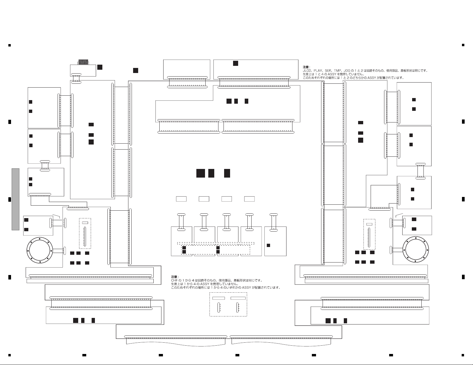
4. BLOCK DIAGRAM
PLAY1 ASSY
(DWX4307)
Y
PLAY2 ASSY
(DWX4308)
or
Z
JLCD1 ASSY (DWX4288)
or
( 1/2- 2/2)
AA AA AA
JLCD2 ASSY (DWX4289)
( 1/2- 2/2)
AB
JOG1 ASSY
(DWX4317)
or
AC
JOG2 ASSY
(DWX4318)
AD
AB AB
JLCD1 ASSY (DWX4288)
or
( 1/2- 2/2)
AA AA AA
JLCD2 ASSY (DWX4289)
( 1/2- 2/2)
AB AB AB
JOG1 ASSY
(DWX4317)
or
AC
JOG2 ASSY
(DWX4318)
AD
Note:
The 1 and 2 Assys of JLCD, PLAY, SER, TMP and JOG Assys have the same circuitry, parts, and board shapes.
Only printed information is different, because their part numbers and wiring numbers are different.
They are handled similarly in their production management.
Therefore, either 1 or 2 Assy of the respective Assys is assembled in the respective place.
Note:
The 1 to 4 Assys of CHF Assys have the same circuitry, parts, and board shapes.
Only printed information is different, because their part numbers and wiring numbers are different.
They are handled similarly in their production management.
Therefore, either 1, 2, 3 or 4 Assy of the respective Assys is assembled in the respective place.
5
6 7 8
XDJ-XZ
4. BLOCK DIAGRAM
4.1 OVERALL WIRING DIAGRAM (1/2)
5
6 7 8
13
D
C
B
A
E
F
14
!
!
!
!
!
!
CN3603
CKS6646
1NC2
GND
3
VGL4VCC5VGH
6
NC
7V18
V29V310V4
11
V512V6
13V714
V8
15
V9
16
V10
17
NC
18
NC
19
DITH
20
VCOM
21
AVDD
22
AGND
23
GND
24
UPDN
25
VCC
26
SHLR
27
STBYB
28
RSTB29MODE
30
VSD
31
HSD
32
DE
33
DCLK
34B735B636
B5
37
B4
38B339
B240B1
41B042
G7
43
G6
44
G545G4
46G347
G2
48G149
G050R7
51
R6
52
R5
53
R4
54
R355R256R1
57
R0
58
VCC
59
AVDD
60
AGND
B2P3-VH
CN1
1.NEUTRAL
3.LIVE
CN2
B10B-PASK
1
V+12
2
V+12
3
V+12
4
V+12A
5
V+12E
6
GNDD
7
GNDD
8
GNDD
9
GNDD
10
standby
DKN1237
JA2001
CKS4428
CN3602
1
2
CN3604
CKS6625
1
YT
2
XR
3YB4
XL
CN3601
CKS6543
1 GNDD
2 V+5R2D
3 V+5R2D
4 GNDD
5
GNDD
6 GNDD
7 LED_L1
8 LED_L2
9 LED_L3
10
LED_L411LED_L5
12 KEY3
13
GNDD
14 GNDD
15 LVDS0_CLKP
16 LVDS0_CLKN
17 GNDD
18 GNDD
19 GNDD
20 LVDS0_P2
21 LVDS0_N2
22 GNDD
23
GNDD
24 GNDD
25
LVDS0_P1
2
6 LVDS0_N1
27 GNDD
28
GNDD
29 GNDD
30 LVDS0_P0
31 LVDS0_N0
32 GNDD
33 GNDD
34 LED_L6
35
LED_L7
36 LED_L8
37 LED_L9
38 V+3R3D
39 V+3R3D
40 GNDD
41 TCP_SCL
42 GNDD
43
TCP_SDA
44 TCP_xINT
45 GNDD
46 BL_A
47 BL_A
48 BL_C
49 BL_C
50 GNDD
51
ENC2
52 ENC1
53 GNDD
54 LED_L10
55 LED_L11
56
LED_L12
57 GNDD
58 KEY1
59 KEY2
60 GNDD
AKM1277
CN4301
1
V+5VBUS12V+5VBUS1
3
GNDUSB1
4
USBDN1_N5USBDN1_P6GNDUSB1
AKM1277
CN4302
1
V+5VBUS22V+5VBUS23GNDUSB24USBDN2_N5USBDN2_P6GNDUSB2
DKB1118
JA4301
VBUS
D-
D+
GND
RT1
RT2
DKB1118
JA4302
VBUS
D-
D+
GND
RT1
RT2
CKS6645
CN105
1
GNDD2V+3R3D23V+3R3D2
4
V+3R3D25GNDD
6
JU1_MOSI
7
GNDD8JU1_MISO
9
GNDD10JU1_SCLK11GNDD12GNDD
13
GNDD
14
xRDY115GNDD16PNL_SCLK
17
GNDD
18
PNL_MOSI19GNDD
20
PNL_MISO21GNDD22PNL_CONT23PNL_xCS2
24
PNL_xCS125GNDD
26
PNL_REQ27ERP_CONT28ERP_REQ29GNDD30ERP_SCLK
31
GNDD32ERP_MOSI33GNDD34ERP_MISO
35
GNDD36ERP_WRITE37ERP_xCS38GNDD39ERP_IMX_POR40GNDD41JU2_MOSI42GNDD43JU2_MISO
44
GNDD
45
JU2_SCLK46GNDD
47
GNDD48GNDD49xRDY250GNDD
CKS6645
CN104
1
GNDD2GNDD3GNDD
4
GNDD_AD_SH
5
GNDD_AD_SH6CH4_FADER7GNDD_AD_SH8CH2_FADER
9
GNDD_AD_SH10CH1_FADER11GNDD_AD_SH
12
CH3_FADER
13
GNDD_AD_SH14CROSS_FADER
15
GNDD_AD_SH16V+3R3D2_AD_SH
17
V+3R3D2_AD_SH
18
GNDD19GNDD20V+5LED
21
V+5LED
22
V+5LED23GNDD_LED24GNDD_LED25GNDD_LED26GNDD_LED27GNDD_LED
28
GNDD_LED
29
V+9LED
30
V+9LED
31
V+9LED32GNDD_LED33GNDD_LED34V+12BL35V+12BL
36
GNDD37GNDD38GNDD
39
PWR_ON40GNDD41FAULT_DET42GNDD
43
ERP_xAMUTE
44
GNDD
45
MAS_VR_MUTE46GNDD47V+5E
48
V+5E49GNDD50GNDD
AKP7199
CN102
1
GNDD
2
V+9LED3V+9LED
4
GNDD_LED5GNDD_LED
6
GNDD_LED
7
V+5LED8V+5LED
9
GNDD10V+5D
11
GNDD12GNDD
13
V+12D
14
V+12D
15
V+12D
16
GNDD17GNDD
18
V+12L
19
GNDD
CN101
CKS6543
1 GNDD
2 GNDD
3 PWR_ON
4 GNDD
5 GNDD
6 GNDD
7 GNDD
8 GNDD
9 V+5E
10 GNDD
11 V+3R3D
12 GNDD
13 AUX_GAIN_SEL
14 GNDD
15 DAC_BCLK
16 GNDD
17 ADAT_HP
18 GNDD
19 DAC_LRCK
20 GNDD
21 ADAT_MIC
22 GNDD
23 ADC_LRCK
24 GNDD
25 ADC_BCLK
26 GNDD
27 ADDA_xRST
28 GNDD
29 ADAT_AUX
30 GNDD
31 ADAT_CH3
32 GNDD
33 ADAT_CH4
34 GNDD
35 CH3_SEL
36 GNDD
37 CH4_SEL
38 GNDD
39 DSP_MCLK
40 GNDD
41 ADAT_BOOTH
42 GNDD
43 ADAT_MASTER
44 GNDD
45 ADAT_SEND
46 GNDD
47 I2C_DAC_SDA
48 GNDD
49 I2C_DAC_SCK
50 GNDD
51 MAS_ATT_6dB
52 GNDD
53 MAS_ATT_12dB
54 GNDD
55 A_FDET
56 GNDD
57 MAS_VR_MUTE
58 GNDD
59 ERP_xAMUTE
60 GNDD
AKM1277
CN1801
1
V+5USBA1_H2V+5USBA1_H
3
GNDD
4
USBDN1_N
5
USBDN1_P
6
GNDD
AKM1277
CN1802
1
V+5USBA2_H2V+5USBA2_H
3
GNDD
4
USBDN2_N5USBDN2_P
6
GNDD
NM
CN2151
1
V+3R3D
2
ENET_MDC
3
ENET_MDIO
4
ENET_CRS_DV
5
ENET_RX_ER
6
ENET_TX_EN
7
ENET_RXD0
8
ENET_RXD1
9
ENET_TXD0
10
ENET_TXD1
11
ENET_ETHER_INT
12
ENET_xRST
13
ENET_REF_CLK
14
GNDD
NM
CN1301
1
V+3R3D
2
SD_D2
3
SD_D3
4
SD_CMD
5
SD_CLK
6
SD_D0
7
SD_D1
8
SD_CDN
9
SD_WP
10
GNDD
CN1302
NM
1
V+3R3D
2
TXD
3
RXD
4
GND
NM
CN1401
1
V+3R3D
2
NC
3
JTAG_TRRSTN
4
JTAG_TDI
5
JTAG_TMS
6
JTAG_TCK
7
JTAG_TDO
8
JTAG_RSTN
9
JTAG_DEN(NC)
10
JTAG_MOD(NC)
11
GNDD
12
GNDD
CN103
CKS6543
1
GNDD
2
V+5R2D3V+5R2D
4
GNDD
5
GNDD
6
GNDD
7
LED_L18LED_L29LED_L310LED_L411LED_L5
12
KEY313GNDD14GNDD
15
LVDS0_CLKP16LVDS0_CLKN
17
GNDD18GNDD19GNDD
20
LVDS0_P221LVDS0_N2
22
GND
D
23
GNDD
24
GNDD
25
LVDS0_P126LVDS0_N1
27
GNDD28GNDD
29
GNDD
30
LVDS0_P031LVDS0_N0
32
GNDD33GNDD
34
LED_L635LED_L7
36
LED_L837LED_L9
38
V+3R3D39V+3R3D
40
GNDD
41
TCP_SCL
42
GNDD
43
TCP_SDA
44
TCP_xINT
45
GNDD
46BL_A
47
BL_A48BL_C49BL_C
50
GNDD
51
ENC252ENC1
53
GNDD
54
LED_L1055LED_L1156LED_L12
57
GNDD
58
KEY1
59
KEY260GNDD
NM
CN2301
1
V+3R3D2
2
V+3R3D2
3
SH_ASEMD
4
SH_TCK
5
SH_TRST
6
SH_TDO
7
SH_ASEBRK
8
SH_TMS
9
SH_TDI
10
SH_RESET
11
GNDD
12
GNDD
NM
CN2601
1
V+3R3D
2
V+3R3D
3
DSP_TMS
4
DSP_TDI
5
DSP_TDO
6
DSP_TCK
7
DSP_EMU
8
DSP_TRST
9
GNDD
10
GNDD
AKM7077
CN5001
1
GNDD
2
V+9LED3V+9LED4GNDD_LED5GNDD_LED6GNDD_LED
7
V+5LED8V+5LED
9
GNDD10V+5D11GNDD12GNDD13V+12D14V+12D
15
V+12D
16
GNDD17GNDD18V+12L
19
GNDD
CN5002
CKS6543
1
GNDD
2
GNDD
3
PWR_ON
4
GNDD
5
GNDD
6
GNDD
7
GNDD
8
GNDD
9
V+5E
10
GNDD
11
V+3R3D1
12
GNDD
13
AUX_GAIN_SEL
14
GNDD
15
DAC_BCLK
16
GNDD
17
ADAT_HP
18
GNDD
19
DAC_LRCK
20
GNDD
21
ADAT_MIC
22
GNDD
23
ADC_LRCK
24
GNDD
25
ADC_BCLK
26
GND
D
27
ADDA_xRST
28
GNDD
29
ADAT_AUX
30
GNDD
31
ADAT_CH3
32
GNDD
33
ADAT_CH4
34
GNDD
35
CH3_SEL
36
GNDD
37
CH4_SEL
38
GNDD
39
DSP_MCLK
40
GNDD
41
ADAT_BOOTH
42
GNDD
43
ADAT_MASTER
44
GNDD
45
ADAT_SEND
46
GNDD
47
I2C_DAC_SDA
48
GNDD
49
I2C_DAC_SCK
50
GNDD
51
MAS_ATT_6dB
52
GNDD
53
MAS_ATT_12dB
54
GNDD
55
A_FDET
56
GNDD
57
MAS_VR_MUTE
58
GNDD
59
ERP_xAMUTE
60
GNDD
CN5601
09R-1.25FJ
1
GNDA_MIC
2
V+15A
3
GNDA_MIC
4
V-15A
5
GNDA_MIC
6
MIC2
7
GNDA_MIC
8
MIC1
9
GNDA_MIC
AKM1277
CN6401
1
HP_R
2
GNDA_HP
3
GNDA_HP4A_MUTE
5
GNDA_HP
6
HP_L
DKN1661
CN6601
1
V+12
2
V+123V+124V+12A5V+12E
6
GNDD7GNDD
8
GNDD9GNDD10standby
CN7602
09P-1.25FJ
1
GND_MIC
2
V+15A
3
GND_MIC
4
V-15A
5
GND_MIC
6
MIC2
7
GND_MIC
8
MIC1
9
GND_MIC
CKS3561
CN7601
1
MIC2_IN
2
MIC2_OUT
3
GND_MIC4GND_MIC
5
MIC1_OUT
6
MIC1_IN
CKS3533
CN7751
1
MIC2_IN
2
MIC2_OUT3GND_MIC
4
GND_MIC
5
MIC1_OUT
6
MIC1_IN
KM200NA6L
CN7701
1
HP_R
2
GNDA_HP3GNDA_HP
4
A_MUTE
5
GNDA_HP
6
HP_L
CKS6645
CN4508
1
GNDD2GNDD3V+5E
4
V+5E5GNDD
6
MAS_VR_MUTE
7
GNDD
8
ERP_xAMUTE
9
GNDD
10
FAULT_DET
11
GNDD
12
PWR_ON
13
GNDD
14
GNDD15GNDD
16
V+12BL
17
V+12BL
18
GNDD_LED19GNDD_LED
20
V+9LED21V+9LE
D
22
V+9LED
23
GNDD_LED24GNDD_LED25GNDD_LED26GNDD_LED
27
GNDD_LED28GNDD_LED
29
V+5LED
30
V+5LED31V+5LED
32
GNDD33GNDD
34
V+3R3D2_AD_SH35V+3R3D2_AD_SH
36
GNDD_AD_SH
37
CROSS_FADER
38
GNDD_AD_SH
39
CH3_FADER
40
GNDD_AD_SH
41
CH1_FADER
42
GNDD_AD_SH
43
CH2_FADER
44
GNDD_AD_SH
45
CH4_FADER
46
GNDD_AD_SH47GNDD_AD_SH
48
GNDD
49
GNDD50GNDD
CKS6645
CN4505
1
GNDD
2
xRDY2
3
GNDD4GNDD5GNDD
6
JU2_SCLK
7
GNDD
8
JU2_MISO
9
GNDD
10
JU2_MOSI
11
GNDD
12
ERP_IMX_POR
13
GNDD
14
ERP_xCS
15
ERP_WRITE
16
GNDD
17
ERP_MISO
18
GNDD
19
ERP_MOSI
20
GNDD
21
ERP_SCLK
22
GNDD
23
ERP_REQ
24
ERP_CONT
25
PNL_REQ
26
GNDD
27
PNL_xCS128PNL_xCS229PNL_CONT
30
GNDD
31
PNL_MISO
32
GNDD
33
PNL_MOSI
34
GNDD
35
PNL_SCLK
36
GNDD
37
xRDY1
38
GNDD
39
GNDD40GNDD
41
JU1_SCLK
42
GNDD
43
JU1_MISO
44
GNDD
45
JU1_MOSI
46
GNDD
47
V+3R3D248V+3R3D249V+3R3D2
50
GNDD
TFT LCD
DWX4375-
USB B
UCOM
USB1
PF06PP-D37
6P,L=375mm
DKP3993CRIMP CONNECTOR
10P,L=260mm AWG 22
NEUTRAL
EARTH
LIVE
POWER CORD
/AXJ DDG1114/JXJ DDG1110/LWSYXJ ADG1244/UXJCB DDG1108-
DKP3994(AWG16)
TOUCH PANEL DSX1130-
USB2
MASTER1MASTER2 BOOTH
MIC2MIC1
CH3
CH4
AUX
DKB1093- DKB1093-
DKB1122(Au Plating)
DKN1653- DKN1653-
DKB1090(Au Plating)
DKB1090(Au Plating)
DKB1122(Au Plating)
DKB1124(XLR+TRS Combo+SW)
DKB1124(XLR+TRS Combo+SW)
Head Phone
DKN1669- XKN3017-
TRS Mini TRS
FPC 1.0mm/4P
L=50mm
FPC 0.5mm/60P
L=31.14mm
L= 60mm
JA5201 JA5401JA5601
DDD1951-(REVERSE FACE)
FFC 0.5mm/60P
L=345mm
DDA1094-
SHIELDED CONN-CABLE
L=184mm AWG #26/#28
FOR DEBUG
SD BOOT UART LAN
JA7702 JA7701
JA6002 JA6003
JA6001
RL
JA6201 JA6202
JA7602JA7601
RL
AKN7115
JA2152
LAN
AKN7115
JA2151
LAN
AKN7115
JA2153
LAN
DKN1652-
R
JA6401
SEND
DKN1652-
L
JA6402
MIXER JTAG i.MX6 JTAGD810 JTAG
DDD1950-(REVERSE FACE)
FFC 0.5mm/60P
L=60mm
CH3
CH4
EXTENSION
DDD1953-(SAME FACE)
FFC 0.5mm/50P L=510mm
DDD1952-(SAME FACE)
FFC 0.5mm/50P L=570mm
DDA1094-
SHIELDED CONN-CABLE
L=184mm AWG #26/#28
AC INLET
( 1/15- 15/15)
A A
MAIN ASSY (DWX4287)
A
( 1/12- 12/12)
B B
AUDIO ASSY (DWX4298)
B
( 1/4- 4/4)
AE AE AE
LCDB ASSY (DWX4291)
AF
SW POWER
SUPPLY
(DWR1548)
MCIN ASSY
(DWX4300)
C
MCTR ASSY
(DWX4302)
D
USBA ASSY
(DWX4294)
E
HPJK ASSY
(DWX4301)
F
-
When ordering service parts, be sure to refer to "EXPLODED VIEWS and PARTS LIST" or "PCB PARTS LIST".
-
The > mark found on some component parts indicates the importance of the safety factor of the part.
Therefore, when replacing, be sure to use parts of identical designation.
-
: The power supply is shown with the marked box.
F
E
D
C
B
A
4.2 OVERALL WIRING DIAGRAM (2/2)
1
2 3 4
XDJ-XZ
1
2 3 4
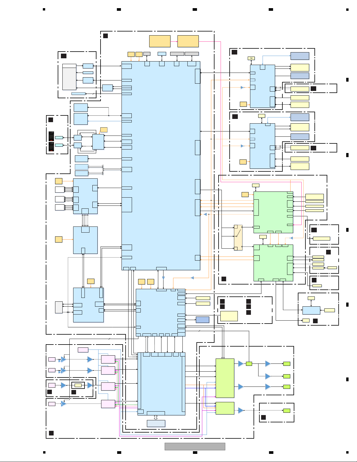
95.962 MHz
SPI 1MHz
2in (RETURN/SAMPLER)
4in (CH3/CH4/REC/SEND)
4out (CH1~CH4)
TDM_PCIN_DATA1
TDM_PCOUT_DATA1
HPI BUS
TDM_PCOUT_DATA2
MIXER_DSP_SCK
MIXER_DSP_xEN
MIXER_DSP_MISO
MIXER_DSP_MOSI
MIXER_DSP_xCS
R SPI 11MHz
DSP_xRST
ADDA_SDA
ADDA_SCL
HP
3
MAS_ATT6 dB
MAS_ATT12 dB
SPI 66MHz
SPI 66MHz
2
12
I2C
PNL_xCS1
SUBU_RST
ERP_xRST
ERP_WRITE
xRST
ERP_WRITE
xRST
SUBU_RST
PNL_xRST
SPI(PNLM UCOM-XPAD)
CDC_CLK
CDC_MOSI
CDC_MISO
CDC_xCS
CDC_xINT
CDC_LED1
CDC_LED2
CDC_LED3
X2301
Xtal
48.000 MHz
X2302
Xtal
13.3333 MHz
X2151
Xtal
25 MHz
X1402
Xtal
24 MHz
X1401
JTAG
SJC
32.768kHz
X3201
Xtal
13.3333MHz
X3001
Xtal
13.3333MHz
PWR_ON
MIC1
MIC2
CH3
AUX
CH4
FAULT_DET
Touch Panel
7inch LCD Module
Touch Panel
Control IC
AK4187-
V+3R3D_Pullup
LVDS Receiver
BU90R104
IC303
Backl ight Driver
IS31BL3555-ZLS4
LCD
xReset
I2C
I2C
I2C
AUTH_xRST
IC1101
Apple Authentication IC
H337S3959-TBB
IC502
PMIC
MMPF0100F0AEP-K
LCD LED
I2C3
I2C2
I2C1
USB_H1_DP
USB_H1_DN
LDB
PWM
GPIO
GPIO
GPIO
GPMI
MMDC
GPIO
[ ENET ]
MDIO
MDC
RX_ER
TX_ER
RXD0
RXD1
TXD0
TXD1
USB_OTG_DP
USB_OTG_DN
USB_OTG_VBUS
AUD3 AUD5
Serial IF
Serial IF
Serial IFSSI3SSI2SSI0D0~D15..etc
UFPI IF
EMIFB Interface
IC2502
W9812G6KH-6-K
SDRAM Parallel 16bit Bus
128 Mbit
McASP0
AXR1[0]
McASP0
AXR1[11]
McASP0
AXR0[2]
BOOT
or SPI 0
xRESET
ADAT_MASTER
ADAT_BOOTH
ADAT_SEND
DAC_BCLK
MCLK
ADDA_xRST
McASP0
McASP0
DAC_LRCLK
ADAT_CH3
ADAT_CH4
ADAT_MIC12
ADAT_AUX
ADC_BCLK
ADC_LRCLK
ADDA_xRST
MCLK
OSCIN
ADAT_HP
TCLKC
TCLKD
AN6-8
AN0-4
R SPI 0
SCL0
SDA0
GPIO
GPIO
GPIO
VBUS
SDA2
SCL2
VBUS
DP
DM
xRES
GPIO
ECSPI5
GPIO
GPIO
GPIO
GPIO
GPIO
GPIO
GPIO
GPIO
GPIO
Mixer KEY
Mixer LED
TC74HC4051AF
Others Mixer VR
EFSW KEY
(CH1-CH4)_CFX_VR
AUX_VR_AD
#RESET
Serial IF Serial IF
AD
GPIO
GPIO
GPIO
GPIO
GPIO
GPIO
xRES
(88pin)
TCLKA
TCLKB
TIOC2B
TCLKA
TCLKB
TIOC2B
RSPI
RSPI
GPIO
xRES
(88pin)
RSPI
RSPI
JTAG
Update
Connector
AD
#RESET
IC4503
RESET IC
PST8430N-TLB
DECK VR
PAD 8*2DECK
DECK KEY/LED
Serial IF
CLK_OUT
XIN
ECSPI4
ECSPI2
ECSPI3
FAULT_DET
ERP_xCS
OE1
OE2
ERP_SCLK
ERP_MISO
ERP_MOSI
SW_ERP_SCLK
SW_ERP_MISO
SW_ERP_MOSI
SW_PNL_SCLK
SW_PNL_MISO
SW_PNL_MOSI
PNL_MCLK_3M
ERP_PNL_WRITE
PNL_REQ
CNVSS
Debug
CLK0
TXD0
RXD0
ERP_CONT
ERP_REQ
ERP_WRITE ERP_WRITE
SPI 1.5 MHz
ECSPI 4
ERP_SCLK
ERP_MISO
ERP_MOSI
ERP_xCS
PNL_xCS1
PNL_CONT
ERP_WRITE
BRWS_ENC1
BRWS_ENC2
SPI 2 MHz
SPI [PANEL M UCOM-MIXER UCOM]
PNL_SCLK
PNL_MOSI
PNL_MISO
PNL_xCS2
LCD BROWSE
ENCODER
LCD KEY1-3
CH1_FADER
CH2_FADER
CH3_FADER
CH4_FADER
CROSS_FADER
MIXER_xRST
SPI
MIXER_MOSI
MIXER_MISO
MIXER_xRDY
MIXER_SCLK_INV MIXER_SCLK
GPIO
USBAHUB_xRST
I2C
HS(480 Mbps)
HS(480 Mbps)
HS(480 Mbps)
OCS
USBA1
USBA2
OCS
16 bit
16 bit
32 bit
IC1805
USBA HUB
TUSB4020BIPHP-
TLB
IC1803
Hi-SideSW
TPS2557DRB
IC1804
Hi-SideSW
TPS2557DRB
IC1102
Nand Flash
MX30LF2G18AC-TI-K
IC901
DDR3 4Gbit
K4B4G1646E-BYMA-K
IC902
DDR3 4Gbit
K4B4G1646E-BYMA-K
LAN Connector
AKN7115-A
RXIP4
RXIN4
TXOP4
TXON4
RESETB
MDIO
MDC
IC2151
LANHUB IC
RTL8309M-CG-K
IC2001
USB/LAN Conversion IC
RTL8152B-VB-CG-TBB
IC2303
SPI Flash 16Mbit
W25Q16JVSSIQ-K
IC701
MAIN UCOM
i.MX6 Quad
MCIMX6Q6AVT10AD-K
(Core 996 MHz)
IC2302
MIXER UCOM
R5S72690W266FP-K
(266 MHz)
IC4502
ERP UCOM
M16C64(100pin)
R5F364AENFA-U0-K
IC3202
JOG LCD UCOM2
R5S72690W266FP-K
IC3002
JOG LCD UCOM1
R5S72690W266FP-K
IC3203
SPI Flash 64 Mbit
W25Q64JVSSIQ-K
JOG LCD
TFT Module
DWX4228-
JOG LCD
TFT Module
DWX4228-
IC3206
SDRAM 64 Mbit
W9864G6KH-5-K
PLAY/CUE KEY
PLAY/CUE LED
LOOP IN/OUT LED
PLAY/CUE KEY
PLAY/CUE LED
LOOP IN/OUT LED
JOG(Rotate)
JOG(Rotate)
JOG(Touch)
Sheet SW
JOG(Touch)
Sheet SW
IC4505
PANELM UCOM
M16C64(100pin)
R5F364AENFA-U0-K
IC2501
DSP
D810K013DZKB400-K
(400 MHz)
IC5802
DAC 4ch Multi
AK4458VN-TLB
Power Detection
Circuit2
IC3401
XPAD
Control IC
ATSAMD20E15A-MU-TBB
XPAD
To SMPS
JTAG
LED
A_FDET
Power Detection
Circuit1
ATT
Master1
Master2
Booth
IC5801
DAC
AK4384ET-TBB
IC2002
USBB HUB 4ch
TUSB4041IPAP-TLB
IC5204
AK5386VT
IC5404
AK5386VT
IC5604
AK5358AET
IC5603
AK5358AET
RXIP2
RXIN2
TXOP2
TXON2
RXIP0
RXIN0
TXOP0
TXON0
USBB
Connector
CH3_SEL
X5101
22.579 MHz
Analog
Trim
AUX_GAIN_SEL
MCLK
CH4_SEL
USB_DM_UP
USB_DP_UP
USB_DM_DN1
USB_DP_DN1
SDA
SCL
I2C
USB_VBUS
RXIP6
RXIN6
TXOP6
TXON6
MDIP0
MDIN0
MDIP1
MDIN1
U2DM
U2DP
IMX_USB_OTG_DP
IMX_USB_OTG_DM
I2S DECK1
I2S DECK2
I2S REC
USB_DM_DN2
USB_DP_DN2
USB_DM_DN3
USB_DP_DN3
USBLAN_DP
USBLAN_DM
CH3
CH4
Extention
LAN Connector
AKN7115-A
LAN Connector
AKN7115-A
EN
EN
LVDS (33 MHz)
PWM
BL_EN
SRC SD3
CSI0_DAT10
CSI0_DAT11
UART
SD BOOTConnector
BOOT Config
SPI 2.5 MHz
ECSPI 3
JU1_SCLK
JU1_MOSI
JU1_MISO
JU1_xRDY
SPI 2.5 MHz
ECSPI 2
JU2_SCLK
JU2_MOSI
JU2_MISO
JU2_xRDY
SPI/CS
For only update
IC4501
74LCX244FT-TBB
LCD_SCK
LCD_TXD
LCD_CS
LCD_xRST
DATA(R/G/B)
6bit*3
LCD_SCK
LCD_TXD
LCD_CS
LCD_xRST
DATA(R/G/B)
6bit*3
IC3003
SPI Flash 64 Mbit
W25Q64JVSSIQ-K
IC3007
SDRAM 64 Mbit
W9864G6KH-5-K
X1801
Xtal
24 MHz
X2001
Xtal
25 MHz
X2002
Xtal
24 MHz
X4501
Xtal
16 MHz
Xtal
AE
LCDB ASSY
AA
JLCD1 ASSY
AB
AC
JLCD2 ASSY
AF
SW POWER
SUPPLY
USBA ASSY
E
HPJK ASSY
F
XPAD ASSY
Q
CHF1 ASSY
J
CHF2 ASSY
K
CHF3 ASSY
L
CHF4 ASSY
M
CRFD ASSY
N
EFSW ASSY
I
JOG1 ASSY
AD
JOG2 ASSY
MIXER
ASSY
H
UCOM ASSY
G
AUDIO ASSY
B
MCIN ASSY
C
MCTR ASSY
D
MAIN ASSY
A
5
4.3 OVERALL BLOCK DIAGRAM
5
6 7 8
XDJ-XZ
6 7 8
A
B
C
D
E
F
15
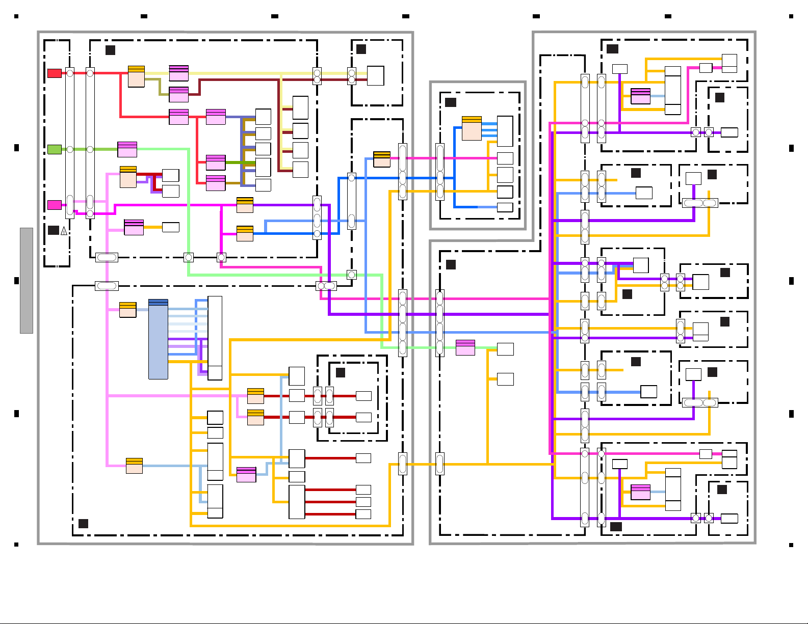
16
IC5801
IC4502
IC4505
DAC
HP
V+10
V+15R6
V-7
V+12A V+18A V+15A
V-15A
V-18A
BL_A/BL_C
V+9A
V+5A
V+5D
V+5E
V+3R3D1
V+5LCDLED
V+5AREF
V+12DHP V+7R5HP
V-7R5HP
V+3R3A
V+1R25L
V+3R3CLK
V+12D
V+12L
V+9LED
V+5D
V+5LED
V+12LED
V+12LED V+12LED
V+12LED
V+12D
V+4R2D
V+1R375CORE
V+9LED
V+9LED
V+9LED V+9LED
V+9LED
V+9LED
V+9LED V+9LED
V+9LED V+9LED
V+9LED V+9LED
V+9LED
V+1R375SOC
V+2R8VHIGH
V+5LED
V+5LED
V+5LED
V+5LED
V+3R0VSNVS
V+1R5DDR
MVREF
V+5E
V+3R3E
V+3R3D1
V+3R3D2
V+3R3D2
V+3R3D2 V+3R3D2
V+3R3D2
V+3R3D2
V+3R3D2 V+3R3D2
V+3R3D2
V+3R3D2 V+3R3D2
V+3R3D2
V+3R3D2
V+3R3D2
V+12D
V+5USB1
V+5USB2
V+12D V+1R25
V+1R1
LCD PWR
IC3605
IC3601
LVDS
Receiver
LCD
BackLight
IC303
IC502
IC901
IC902
IC701
IC2302
IC1101
IC1102
IC2303
IC2501
IC2502
IC501
IC301
IC302
IC1801
IC1802
IC1803
IC1804
IC2002
IC2001
IC2151
IC1805
IC6605
IC6605
IC6402
IC5204
IC5404
IC5201
IC5202
IC5401
IC5402
IC7601
IC7602
IC5601
IC5602
IC6001
IC6002
IC6201
IC6202
IC5604
IC5603
IC5802
IC6610
IC6603
AUDIO
CLK Buff
IC6604
V+12A
IC6607
IC6609
Backlight
LAN 2
LAN HUB
LAN 1
USB-LAN
FLASH
USB B
USBA
HUB
Hi-Side
SW
Hi-Side
SW
USB HUB
USB1
SDRAM
DSP
LAN 3
LED
IC6608
V+12E
IC6612
IC6606
IC6611
IC6601
HP AMP
OpAmp
HP
DDR3
MAIN
UCOM
IC6602
IC4508
MIXER
uCOM
USB2
OpAmp
MIC1-2
OpAmp
BOOTH
OpAmp
MASTER
OpAmp
AUX1
PANELM
uCOM
Auth IC
NAND
FLASH
XPAD
IC3001
IC3002
IC3003
IC3007
PLAY
LED
MIXER
LED
OpAmp
CH1-4
ErP
uCom
TCP IC
SDRAM
JOG LCD
uCOM
FLASH
CN2
CN6601
CN5601
CN5001
CN102
CN103
CN104
CN4508
CN105
CN101
CN5001
CN102
CN102
CN5001
CN5002
CN7602
V+12E
454
5
V+12
V+12D
V+12L
2
4
2
4
2
1
3
2
1
ADC
AUX
ADC
CH3/4
ADC
MIC1/2
DAC
MASTER
BOOTH
SEND
10
10
18
18
15 9
9
CN3001
CN7951
2 2
CN4515
CN4518
CN4516
CN3005
CN8102
CN4506
CN7001
CN7003
CN4901
CN7002
CN4509
CN4507
CN4503
CN4504
8
2
3
7
8
7
35
34
48
47
31
30
29
22
21
20
4
3
2
CN4505
17
16
4
3
4
3
8
7
22
21
13
12
30
29
23534
1
2
1
22
21
18
17
22
21
20
31
30
29
49
48
47
191810
9
CN3601
13 14
1513 14
CN3901
32,
28
27
JOG RING
JOG LCD
BL
BL CNT
C.M.
V+1R25L
IC3201
IC3202
IC3203
IC3206
PLAY
LED
SDRAM
JOG LCD
uCOM
FLASH
CN3201
CN8001
2 2
CN3205
6
5
10
9
6
5
10
9
JOG RING
JOG LCD
BL
DCK1 LED
PAD LED
RGB
CN9002
CN9001
2
1
2
1
CN4520
CN4519
30
29
30
29
CN4101
CN3401
DCK1 LED
PAD LED
RGB
EFSW
LED
BL CNT
C.M.
CN4301
CN4302
2
1
2
1
CN1801
CN1802
2
1
2
1
2
18
50
48
49
2
18
24
23
3
1
2
26
23
22
2
6
5
5048 49 27 28
2
8
7
312 2324
49
48
47
46
3
2
39
38
49
48
47
46
3
2
39
38
AF
SW
POWER
SUPPLY
AUDIO ASSY
B
MAIN ASSY
A
USBA ASSY
E
MCIN ASSY
C
AE
LCDB ASSY
UCOM ASSY
G
AA
JLCD1 ASSY
DCK1 ASSY
R
PLAY1
ASSY
Y
MIXER ASSY
H
DCK2 ASSY
T
AB
JLCD2 ASSY
PLAY2
ASSY
Z
EFSW
ASSY
I
XPAD
ASSY
Q
PAD2 ASSY
P
PAD1 ASSY
O
18
15
14
3
F
E
D
C
B
A
4.4 POWER BLOCK DIAGRAM
1
2 3 4
XDJ-XZ
MM1856A50N
BD9851EFV
BD9328EFJ
DCDC
BD9851EFV
REG
DCDC
REG
NJM2831F33
DCDC
DCDC
BD9328EFJ
PMIC
MMPF0100F0AEP
REG
NJM78M15DL1A
1
REG
NJM79M15DL1A
REG
NJM78M09DL1A
REG
NJM7805DL1A
REG
NJM7805DL1A
REG
NJM2872BF33
DCDC
R1290K103A
DCDC
IS31BL3555
REG
NJM2872BF33
DCDC
BD9328EFJ
DCDC
BD9328EFJ
REG
BD00IC0WEFJ
DCDC
BD9328EFJ
DCDC
BD9328EFJ
REG
BD00IC0WEFJ
REG
BD00IC0WEFJ
2 3 4
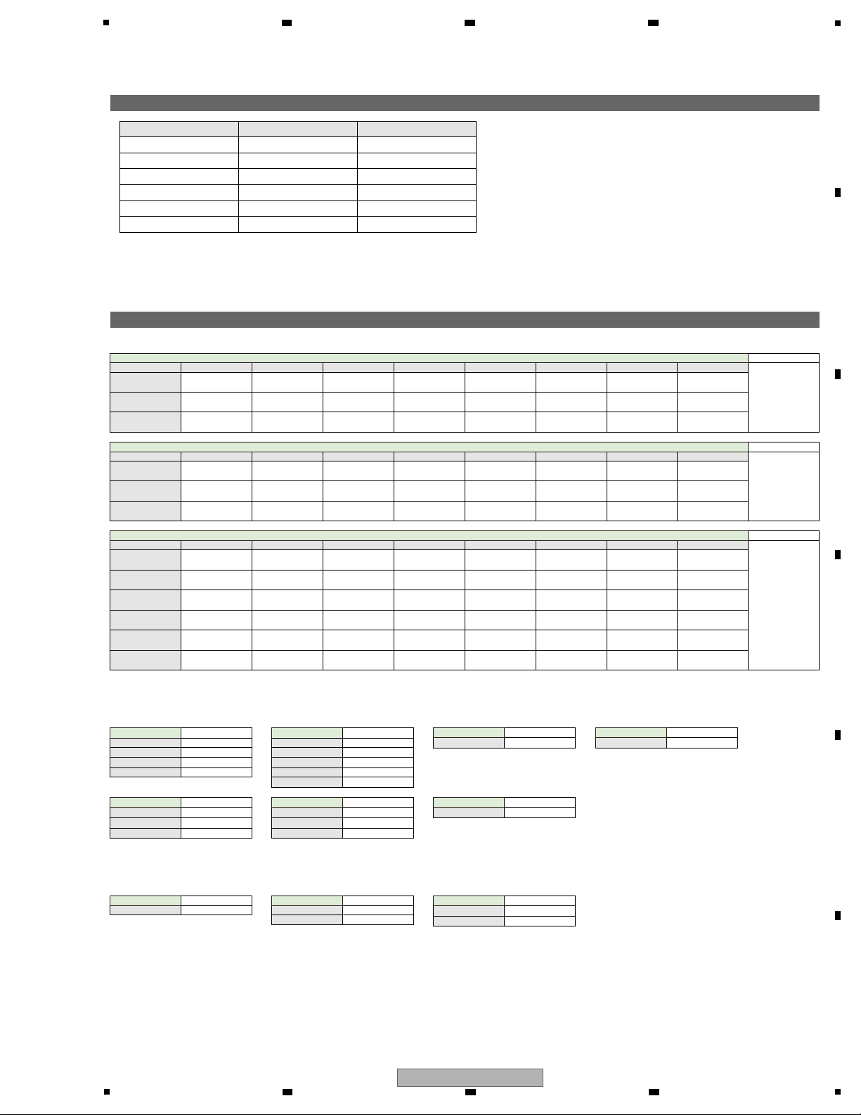
5
UCOM Name Ref No. Assy Name
MAIN(i.MX) IC701 MAIN
MIXER IC2302 MAIN
JOGLCD1 IC3002 JLCD1
JOGLCD2 IC3202 JLCD2
PNLM IC4505 UCOM
ERP IC4502 UCOM
g KEY MATRIX
g DIRECT KEY/TIMER
g DIRECT AD
Control UCOM List
SW/VR (KEY/AD)
GRID0 GRID1 GRID2 GRID3 GRID4 GRID5 GRID6 GRID7
GRID0 GRID1 GRID2 GRID3 GRID4 GRID5 GRID6 GRID7
ERP
DCK1_KEY0
T-SRCH
o
SRCH
m
REV
T-SRCH
p
SLIP
SRCH
n
SHIFT
DCK1_KEY1 VINYL SYNC TMP RESET MASTER 4Beat TMP RANGE MS TMP
DCK1_KEY2 RELOOP MEMORY LOOP IN DELETE LOOP OUT
CUE CALL
d
CUE CALL
c
Control UCOM
Control UCOMDCK1
DCK2
MIXER
ERP
DCK2_KEY0
T-SRCH
o
SRCH
m
REV
T-SRCH
p
SLIP USB1_STOP
SRCH
n
SHIFT
DCK2_KEY1 VINYL SYNC TMP RESET MASTER 4Beat USB2_STOP TMP RANGE MS TMP
DCK2_KEY2 RELOOP MEMORY LOOP IN DELETE LOOP OUT TRK_MARK
CUE CALL
d
CUE CALL
c
Control UCOM
MXR_GRID0 MXR_GRID1 MXR_GRID2 MXR_GRID3 MXR_GRID4 MXR_GRID5 MXR_GRID6 MXR_GRID7
PNLM
MXR_KEY0
CH3 INPUT SEL
PC/LINE/PHONO
CH3 INPUT SEL
PC/LINE/PHONO
AUX_OFF/LINE/POR
TABLE
AUX_OFF/LINE/POR
TABLE
CH4 INPUT SEL
PC/LINE/PHONO
CH4 INPUT SEL
PC/LINE/PHONO
MXR_KEY1
CH3
CUE
CH1
CUE
CH2
CUE
CH4
CUE
FQ_LOW FQ_MID FQ_HI
MXR_KEY2 BFX_CHSEL1 AUTO/TAP SW TAP MXR_QTZ BFX_SEL1
MXR_KEY3
CFX
SPACE
CFX
DUB ECHO
CFX
SWEEP
BFX_CHSEL2
CFX
SPACE
CFX
DUB ECHO
CFX
SWEEP
BFX_SEL2
MXR_KEY4
CFX
NOISE
CFX
CRUSH
CFX
FILTER
BFX_CHSEL3
CFX
NOISE
CFX
CRUSH
CFX
FILTER
BFX_SEL3
MXR_KEY5
BFX
ON/OFF
BFX
c
BFX
d
BFX_CHSEL4
BFX
ON/OFF
BFX
c
BFX
d
BFX_SEL4
Control UCOM DCK2
MIXER
MIXER
LCD
JOG2/JLCD2JOG1/JLCD1 EFSW
CHF1 to 4/CRFPAD1&2
DCK1 Control UCOM
PLAY JOGLCD1 PLAY JOGLCD2
CUE JOGLCD1 CUE JOGLCD2
FBE_SW
PNLM MAS REC/WAKEUP ERP
FBE ON/OFF PNLM PWR_SW ERP
MASCUE
PNLM
Control UCOM Control UCOM
BRWS_ENC
MIXER
FBE_SW
PNLM
Control UCOM Control UCOM
JOG_SW
JLCD1
JOG_SW
JLCD2
JOG1
JLCD1
JOG1
JLCD2
JOG2
JLCD1
JOG2
JLCD2
Control UCOM
TIME
PNLM
Control UCOM Control UCOM
PAD(1 to 8) ERP CHFADER_1 to 4 MIXER
CROSS FADER MIXER
Control UCOM
CH1 to 4_CFX_VR
PNLM
AUX_VR
PNLM
4.5 MATRIX INFORMATION
6 7 8
A
B
C
D
E
5
XDJ-XZ
6 7 8
F
17
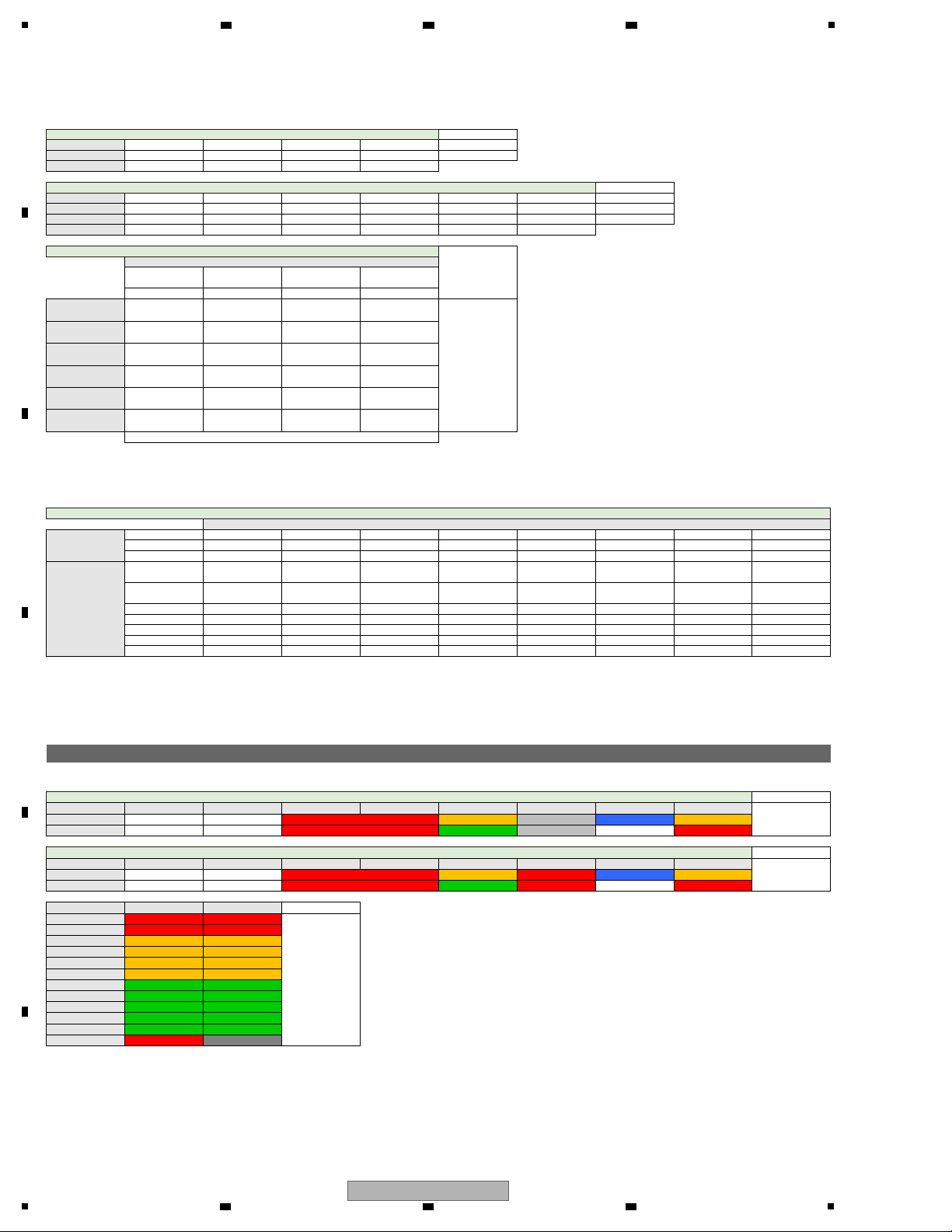
1
g AD KEY (Resistive Dividing Voltage)
g MULTIPLEXER AD
g LED MATRIX
LED
DCK1
DCK2
LCD
MIXER/DCK1
MIXER
PAD1&2
Control UCOM
PADMODE_L HOT CUE AUTO BEAT LOOP SLIP LOOP BEAT JUMP ERP
PADMODE_R HOT CUE AUTO BEAT LOOP SLIP LOOP BEAT JUMP ERP
Voltage(typ) 0.0 V 0.4 V 0.8 V 1.2 V
Control UCOM
LCD_KEY1 QUANTIZE TIME MODE USB2 USB1 LINK rekordbox MIXER
LCD_KEY2 LOAD2 ROTARY SEARCH SHORTCUT FILTER BACK TAG TRACK MIXER
LCD_KEY3 LOAD1 MENU INFO TAG LIST BROWSE MIXER
Voltage(typ) 0.0 V 0.4 V 0.8 V 1.2 V 1.7 V 2.2 V
Control UCOM
SW position
OPEN
(THRU)
A THRU B
OFF - ON
MIC1_SW
(OFF/ON)
- 1.6 V - 0.0 V
MIXER
MIC2_SW
(OFF/ON/)
- 1.6 V - 0.0 V
CH1_FDSW
(A/THRU/B)
3.3 V 1.8 V 1.0 V 0.0 V
CH2_FDSW
(A/THRU/B)
3.3 V 1.8 V 1.0 V 0.0 V
CH3_FDSW
(A/THRU/B)
3.3 V 1.8 V 1.0 V 0.0 V
CH4_FDSW
(A/THRU/B)
3.3 V 1.8 V 1.0 V 0.0 V
Voltage(typ)
VR Select
Multiplexer
SW
Signal
VR_SEL_C 0 0 0 0 1 1 1 1
VR_SEL_B 0 0 1 1 0 0 1 1
VR_SEL_A 0 1 0 1 0 1 0 1
MultiplexerAD
OUTPUT
Signal
MXR_AD0
MIC1_SW
(OFF/ON)
MIC2_SW
(OFF/ON)
MIC1_LOW MIC2_LOW MIC1_MID MIC2_MID MIC1_HI MIC2_HI
MXR_AD1
CH2_FDSW
(A/THRU/B)
CH1_FDSW
(A/THRU/B)
CH3_FDSW
(A/THRU/B)
CH4_FDSW
(A/THRU/B)
CFX_PARAM
EFX_LVD
(Lvel/depth)
HP_MIX HP_LV
MXR_AD2 CH1_HI CH1_MID CH1_LOW CH1 TRIM CH2 TRIM CH2_LOW CH2_HI CH2_MID
MXR_AD3 CH3_HI CH3_MID CH3_LOW CH3 TRIM CH4_HI CH4_MID CH4_LOW CH4 TRIM
MXR_AD2 CH2_MID CH2_LOW CH2_TRIM CH2_HI CH4_TRIM CH4_LOW CH4_HI CH4_MID
MXR_AD3 CH3_MID CH3_LOW CH3_TRIM CH3_HI CH1_TRIM CH1_LOW CH1_HI CH1_MID
MXR_AD4 MAS LV MAS_MID - MAS_LOW MAS_HI - BOOTH_LV
IC: TC74HC4051AF
-
GRID0 GRID1 GRID2 GRID3 GRID4 GRID5 GRID6 GRID7
GRID0 GRID1 GRID2 GRID3 GRID4 GRID5 GRID6 GRID7
ERPDCK1_LED0 REV RELOOP VINYL MASTER
DCK1_LED1 SLIP TMP_RST SYNC MT
Control UCOM
Control UCOM
ERPDCK2_LED0 REV RELOOP USB STOP1 VINYL MASTER
DCK2_LED1 SLIP TMP_RST USB STOP2 SYNC MT
GRID_DIR0 GRID_DIR1 Control UCOM
MXRDCK2_LED0 MASL Lv 15 MASR Lv 15
PNLM
MXRDCK2_LED1 MASL Lv 12 MASR Lv 12
MXRDCK2_LED2 MASL Lv 9 MASR Lv 9
MXRDCK2_LED3 MASL Lv 6 MASR Lv 6
MXRDCK2_LED4 MASL Lv 3 MASR Lv 3
MXRDCK2_LED5 MASL Lv 0 MASR Lv 0
MXRDCK2_LED6 MASL Lv -3 MASR Lv -3
MXRDCK2_LED7 MASL Lv -6 MASR Lv -6
MXRDCK2_LED8 MASL Lv -9 MASR Lv -9
MXRDCK2_LED9 MASL Lv -15 MASR Lv -15
MXRDCK2_LED10 MASL Lv -24 MASR Lv -24
MXRDCK2_LED11 MAS_CLIP
2 3 4
A
B
C
D
E
F
18
XDJ-XZ
1
2 3 4
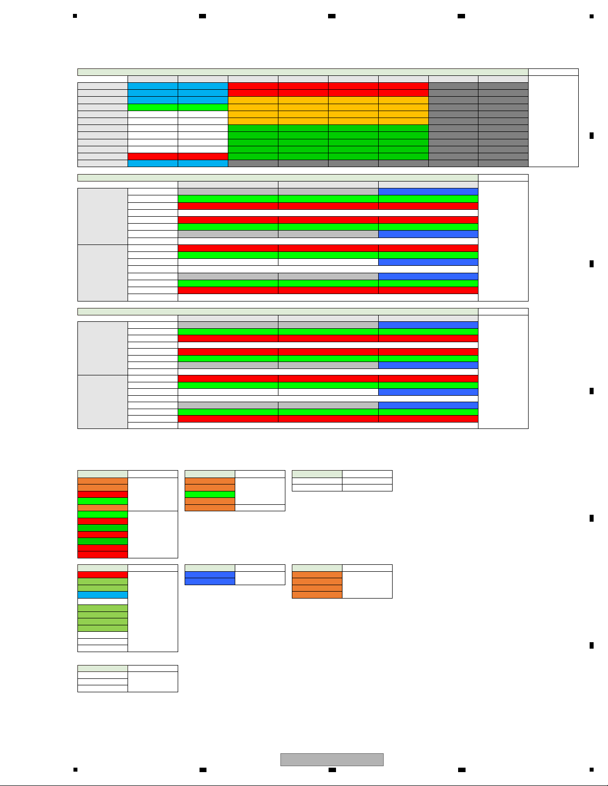
5
g LED DIRECT
MIXER
PAD1
PAD2
Control UCOM
MXR_GRID0 MXR_GRID1 MXR_GRID2 MXR_GRID3 MXR_GRID4 MXR_GRID5 MXR_GRID6 MXR_GRID7
PNLM
MXR_LED0 FQ_LOW FQ_LOW CH1 Lv 15 CH2 Lv 15 CH3 Lv 15 CH4 Lv 15
MXR_LED1 FQ_MID FQ_MID CH1 Lv 12 CH2 Lv 12 CH3 Lv 12 CH4 Lv 12
MXR_LED2 FQ_HI FQ_HI CH1 Lv 9 CH2 Lv 9 CH3 Lv 9 CH4 Lv 9
MXR_LED3 TAP TAP CH1 Lv 6 CH2 Lv 6 CH3 Lv 6 CH4 Lv 6
MXR_LED4 CFX1 CFX1 CH1 Lv 3 CH2 Lv 3 CH3 Lv 3 CH4 Lv 3
MXR_LED5 CFX2 CFX2 CH1 Lv 0 CH2 Lv 0 CH3 Lv 0 CH4 Lv 0
MXR_LED6 CFX3 CFX3 CH1 Lv -3 CH2 Lv -3 CH3 Lv -3 CH4 Lv -3
MXR_LED7 CFX4 CFX4 CH1 Lv -6 CH2 Lv -6 CH3 Lv -6 CH4 Lv -6
MXR_LED8 CFX5 CFX5 CH1 Lv -9 CH2 Lv -9 CH3 Lv -9 CH4 Lv -9
MXR_LED9 CFX6 CFX6 CH1 Lv -15 CH2 Lv -15 CH3 Lv -15 CH4 Lv -15
MXR_LED10 MXR_QTZ MXR_QTZ CH1 Lv -24 CH2 Lv -24 CH3 Lv -24 CH4 Lv -24
MXR_LED11 BFX ON BFX ON
Control UCOM
PADGRID_0 PADGRID_1 PADGRID_2
ERP
PADL_SI0
PADL_SCK0
PAD_RCK
PAD_xG
QA BEAT JUMP_B
QB PAD4_G PAD8_G BEAT JUMP_G
QC PAD4_R PAD8_R BEAT JUMP_R
QD DIMMER CONTROL
QE PAD3_R PAD7_R SLIP LOOP_R
QF PAD3_G PAD7_G SLIP LOOP_G
QG SLIP LOOP_B
QH1 DIMMER CONTROL
PADL_SI1
PADL_SCK1
PAD_RCK
PAD_xG
QA PAD2_R PAD6_R AUTO BEAT LOOP_R
QB PAD2_G PAD6_G AUTO BEAT LOOP_G
QC AUTO BEAT LOOP_B
QD DIMMER CONTROL
QE HOT CUE_B
QF PAD1_G PAD5_G HOT CUE_G
QG PAD1_R PAD5_R HOT CUE_R
QH1 DIMMER CONTROL
Control UCOM
PADGRID_0 PADGRID_1 PADGRID_2
ERP
PADR_SI0
PADR_SCK0
PAD_RCK
PAD_xG
QA BEAT JUMP_B
QB PAD4_G PAD8_G BEAT JUMP_G
QC PAD4_R PAD8_R BEAT JUMP_R
QD DIMMER CONTROL
QE PAD3_R PAD7_R SLIP LOOP_R
QF PAD3_G PAD7_G SLIP LOOP_G
QG SLIP LOOP_B
QH1 DIMMER CONTROL
PADR_SI1
PADR_SCK1
PAD_RCK
PAD_xG
QA PAD2_R PAD6_R AUTO BEAT LOOP_R
QB PAD2_G PAD6_G AUTO BEAT LOOP_G
QC AUTO BEAT LOOP_B
QD DIMMER CONTROL
QE HOT CUE_B
QF PAD1_G PAD5_G HOT CUE_G
QG PAD1_R PAD5_R HOT CUE_R
QH1 DIMMER CONTROL
Control UCOM DCK2DCK1
LCD
XPAD
Control UCOM JLCD1&2 Control UCOM
LOOP IN1
JLCD1
LOOP IN2
JLCD2
JOG1 LED JLCD1
LOOP OUT1 LOOP OUT2 JOG2 LED JLCD2
WAKEUP/MAS REC PLAY2
PLAY1 CUE2
CUE1 CUE MAS PNLM
FBELM
PNLM
MIC1_CLIP
MIC1_INPUT
MIC2_CLIP
MIC2_INPUT
MIC1_ON
MIC2_ON
Control UCOM PAD1&2 Control UCOM MIXER Control UCOM
QTZ(Quantize)
MAIN(I.MX)
PAD1 BLUE(1 to 8)
ERP
CUE CH1
PNLM
USB2 PAD2 BLUE(1 to 8) CUE CH2
USB1 CUE CH3
LINK CUE CH4
RKB(rekordbox)
BROWSE
TAG LIST
INFO
MENU
BROWSE ENC(ILM)
DCK1
DCK2
Control UCOM
CDC_LED1
PNLMCDC_LED2
CDC_LED3
6 7 8
A
B
C
D
5
6 7 8
XDJ-XZ
E
F
19
1
Power cord connected.
The POWER switch (S8401) is set to ON.
It supplies V+12E and starts.
It generates V+3R3E in IC4508 and start.
g STARTUP SEQUENCE
Operation of the power supply monitoring ERP UCOM (P8_4)
It executes the mute of the audio.
Flashes LED of MASTER_REC in red.
It stops the SW POWERSUPPLY output with PWR_ON
signal as "Low".
g Monitoring of the power supply abnormality
Judgment of Update mode
Update
mode
PWR_SW signal "Low" input to EUP UCOM (IC4502).
"Connect USB storage device into top USB1 port" indication.
Firmware updating starts.
Each microcomputer startup.
Start of the power supply monitoring.
Power supply start to each microcomputer (MAIN, MIXER,
JOGLCD, PANELM).
It start supply of 3MHz from CLKOUT (p5_7).
d PANELM UCOM clock.
ERP_WRITE (p6_4) and ERP_PNL_WRITE (p1_4) on
ERP UCOM (IC4502) to "Low". Each microcomputer
(MAIN, MIXER, JOGLCD and PANELM) startup processing
in normal mode.
Reset signal "Low" of each microcomputer input from
ERP UCOM (IC4502) and then, PWR_ON (P8_3) is "High"
and SW POWER SUPPLY start.
All power ICs start generating power.
Reset of each microcomputer is canceled by ERP UCOM (IC4502).
SUBU_RST (p7_2) :
d After inversion, It is connected to the reset terminal of PANELM, JOGLCD UCOM.
ERP_IMX_POR (p8_2) :
d After inversion, It is connected to the reset terminal of MAIN, MIXER UCOM.
LED all light on.
LED all light on d Initial light on
Start completion.
Start of communication with MAIN UCOM.
The audio mute cancellation request reception from MAIN UCOM. And
then, It executes audio mute cancellation after waiting for two seconds.
Reset of ERP UCOM (IC4502) is canceled in 12 pin "High".
ERP UCOM (IC4502) is initialized.
ERP_WRITE (p6_4) and ERP_PNL_WRITE (p1_4) on
ERP UCOM (IC4502) to "High". Each microcomputer
(MAIN, MIXER, JOGLCD and PANELM) startup processing
in update mode.
+ Condition to become the update mode
! When you press the predetermined key on ERP UCOM, and a power is turned on.
! When it judges that update was stopped of the product being completed last time.
(Information during update remains in ERP UCOM.)
Does the abnormality of
the power supply occur?
Yes
No
It is developed the program by Flash ROM. --
Initialization of the built-in / outskirts module.
MAIN UCOM :
(IC701)
Communication start between each microcomputer
MAIN f ERP, MAIN f JOGLCD, MAIN f MIXER, MIXER f PANELM
It is audio mute cancellation request by initialization completion. (MAIN UCOM)
MIXER UCOM :
(IC2302)
PANELM UCOM :
(IC4505)
JOGLCD UCOM :
(IC3002, IC3202)
PANELM UCOM :
LED all light on.
LCD start indication.
!DSP (IC2501) reset
!
Program download to
DSP
!DSP start
LED all light on.
!
X-PAD (IC3401) reset
!
First communication to X-PAD
LED initial light on
LED all light on.
LCD start indication.
5. DIAGNOSIS
5.1 STARTUP SEQUENCE
A
B
2 3 4
C
D
E
F
20
1
XDJ-XZ
2 3 4
5
Before starting troubleshooting, confirm that all cable connectors are properly engaged.
In the following diagnostic procedure, because power will be forcibly supplied even if any power circuit is abnormal, the defective point may produce heat and the
circuit that uses the power supply may fail if power supply continues. Be sure to disconnect the AC power cord some seconds after it is connected during the
diagnostic procedure so that the unit will not remain forcibly powered.
Before replacing a microcomputer, confirm also the items shown below.
Confirm the voltage of ERP UCOM. And, confirm if the reset cancellation
is performed normally.
UCOM Assy : V+3R3E (3.3 V)
IC4502-12 pin (RST) : 3.3 V
If no problem, replace ERP UCOM.
If the voltage is abnormal, confirm the peripheral circuit of ERP UCOM.
In a case where a failure of ERP UCOM
(IC4502) is suspected
Failure in startup and in the communication system
Failure in the power system
Disconnect the AC power cord from the product then remove
R346 (0 ) from the MAIN Assy. Reconnect the AC power cord
then set the Power switch to ON to monitor each power IC.
IMPORTANT: Because the voltage monitoring circuit is disabled,
disconnect the AC power cord within several seconds.
Check the voltage at each block.
Check the circuits or power ICs that use the
power supply with abnormal voltage.
Check if there is no problem in the connection
wires between each boards. If no problem,
check V+12E, V+5E and V+3E, and replace
the defective parts.
A type of abnormality that cannot be detected by
the voltage monitoring circuit is suspected.
Check if the voltage value is within the normal
range, referring to "10.69 VOLTAGES".
Before starting checking the power system, be
sure to check if each power IC is short-circuited
with GND, referring to "10.69 VOLTAGES."
No short-circuit
Check the MASTER REC LED. Check the voltage of FAULT-DET.
Confirmation of
power-failure detection
Light off
3.3 V
0 V
Flashing in red
No startup after pushing the Power switch.
If the MASTER REC LED is flashing in red or the voltage of FAULT-DET is 0 V, it is recommended that the following circuits be confirmed first:
• Peripheral circuits of IC6605/6606 (V+18A/V-18A and V+7R5HP/V-7R5HP generation circuits)
• Q6603, Q6605, D6603, D6606, Q6602, Q6604, D6602, D6605
Reattach R346 (0 ) to the MAIN Assy.
(For enabling the voltage-monitoring function)
Replace the defective parts after checking
that the product operates properly.
Failure in startup and in the
communication system
See the section on "Updating of the firmware
does not start".
Communication among MAIN UCOM (IC701) and MIXER UCOM (IC2302) on MAIN Assy,
ERP UCOM (IC4502) and PANELM UCOM (IC4505) on UCOM Assy have not been established.
Check the connection between MAIN Assy and UCOM Assy.
If no problem, replace MAIN Assy.
If it still not improve, replace UCOM Assy.
After the Power switch is set to ON, the
startup procedure stops in mid-course, with
the message "Connect USB storage device
to top USB1 port" displayed on the LCD.
Failure of previous updating of the firmware
was the cause. (Power failure occurred
during previous updating.)
Perform updating of the firmware.
Startup has been
completed properly.
Startup is not completed.
Startup was not completed,
or updating failed.
After the Power switch is set to ON, the
startup procedure stops in mid-course, with
the message "PIONEER DJ rekordbox"
displayed on the LCD.
Startup is not completed.
6 7 8
5.2 TROUBLESHOOTING
A
B
C
D
5
6 7 8
XDJ-XZ
E
F
21
1
Check if the updating notification circuit on
the UCOM Assy is normal.
Check ERP_WRITE while displaying the
update mode.
Check if data on the USB memory device
have been read. See "Data of the device
(USB memory device, hard disk, etc.)
connected to the USB A connector cannot
be read" in this flowchart.
Check the keys (switches) in the DCK1 Assy,
using the diagnosis in Test mode or referring
to "No operation with keys (switches)."
• USB1 STOP
• RELOOP/EXIT
If the keys (switches) function normally, the
ERP UCOM (IC4502) may be in failure. Replace it.
When the unit is started in Update
mode, does the indication on the LCD
become that for Update mode?
When the unit is started in Update
mode, does the indication on the LCD
become that for Update mode?
Is the voltage at Pin 34 of
CN4502 (ERP_WRITE) 3.3 V?
Updating of the firmware does not start.
Updating not available
Updating not available
Ye s
Ye s
Replace the IC4502 (ERP UCOM).
MAIN UCOM (IC701) cannot recognize the
updating status. Check connection between
the MAIN Assy and UCOM Assy.
Check also the line connected to Pin 36 of
CN105 (ERP_WRITE) on the MAIN Assy.
If no problem, MAIN UCOM (IC701) may be
defective. Replace the MAIN Assy.
USB function is normal.
Check the connection between MAIN Assy and
UCOM Assy. If no problems are found in
peripheral circuits, connectors, or cables,
replace ERP UCOM (IC4502) and PANELM
UCOM (IC4505).
ERP UCOM/PANELM UCOM
Rewriting of which one failed,
the flash ROM or microcomputer?
Rewriting of which one failed,
the flash ROM or microcomputer?
No
No
Check the connection of the periphery of the
corresponding flash ROM. If no problem, replace
the MAIN Assy.
Flash ROM
Updating of the firmware failed.
"Firmware update failed" is displayed.
Updating is not possible, because the program in
the microcomputer is abnormal, the flash ROM,
ERP UCOM or PANELM UCOM is in failure, or
the communication line is in failure.
Check the LCD display during the update.
The updating status of the flash ROM (IC1102) in
the MAIN Assy is displayed on the first line (MAIN).
The updating status of the ERP UCOM (IC4502)
and PANELM UCOM (IC4505) in the UCOM Assy
is displayed on the second line (ERP/SUB).
The updating status of the flash ROM (IC2302) in
the MAIN Assy is displayed on the third line (MIXER).
The updating status of the flash ROM
(IC3003/IC3203) in the JLCD1/JLCD2 Assy is
displayed on the fourth and the fifth lines
(JOGL/JOGR).
If the progress of a status bar is stopped in
mid-course, rewriting of the corresponding ROM
or microcomputer failed.
A
2 3 4
B
C
D
E
F
22
1
2 3 4
XDJ-XZ
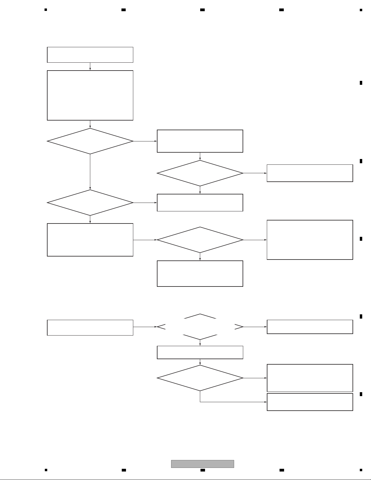
Confirmation of the USB A connector
Confirmation of
USB power
USB power supply has been stopped by
activation of the protection circuit.
Check the voltage at USBA1/USBA2_OCS
after the USB device is unplugged.
The USB device is in failure or consumes
electric current higher than 1000 mA.
Replace the USB device.
Check if the USB device is normal.
Note that a USB device that requires electric
current higher than 1000 mA according to its
specifications must not be used.
To such a USB device, USB power supply will
be stopped by the protection circuit. Check the
voltages at the following points with the USB
device plugged in:
!
MAIN Assy: Pin 8 of IC1803 (USB1_FAULT)
!
MAIN Assy: Pin 8 of IC1804 (USB2_FAULT)
Data from the device (USB memory device,
hard disk, etc.) connected to the USB A
connector cannot be read.
Check that 12 V is supplied to Pin 2 of
IC1801/IC1802 and that no abnormality is
found in their peripheral circuits. Check the
connection between the USBA Assy and
MAIN Assy.
If no problem in the above checks, power IC
(IC1801/IC1802) in the MAIN Assy may be
in failure. Replace the MAIN Assy.
Check the power supply to the USB A connector.
• USBA Assy:
Pin 1, 2 of CN4301/CN4302
• MAIN Assy:
Pin 1, 2 of CN1801/CN1802
Check if the voltage is 5 V ± 0.25.
Is the voltage at each point normal?
Is the voltage at
USBA1/USBA2_OCS 3.3 V?
Ye s
No
No
No
Ye s
Check the peripheral circuits of IC1803/IC1804.
If no problem, replace the MAIN Assy.
Ye s
Check the USB communication line.
• MAIN Assy:
USBDN1_N/P, USBDN2_N/P
If no problem in the above checks, replace
the MAIN Assy.
Is the voltage at
USBA1/USBA2_OCS 3.3 V?
Is the voltage at
USB1/USB2_EN
3.3 V?
3.3 V
0 V
Confirmation of the USB B connector
Does this unit operate properly
on its own when it is not controlled via
the USB B connector?
Does this unit operate properly
on its own when it is not controlled via
the USB B connector?
Is the main unit recognized
by the PC/Mac?
This unit cannot be recognized or controlled
by the PC/Mac that is connected via the
USB B connector.
Ye s
No
Ye s
No
The periphery circuits of USB HUB IC (IC2002)
or MIXER UCOM (IC2302) USB communication
line in the MAIN Assy may be in failure.
Check the power supply to each IC.
If no problem, replace the MAIN Assy.
Check and correct the settings of the
application used on the PC/Mac.
(This unit operates properly.)
See the section on errors in the operating
elements and LEDs.
Check that the driver for the main unit has
been installed on the PC/Mac.
5
6 7 8
A
B
C
D
E
XDJ-XZ
5
6 7 8
F
23
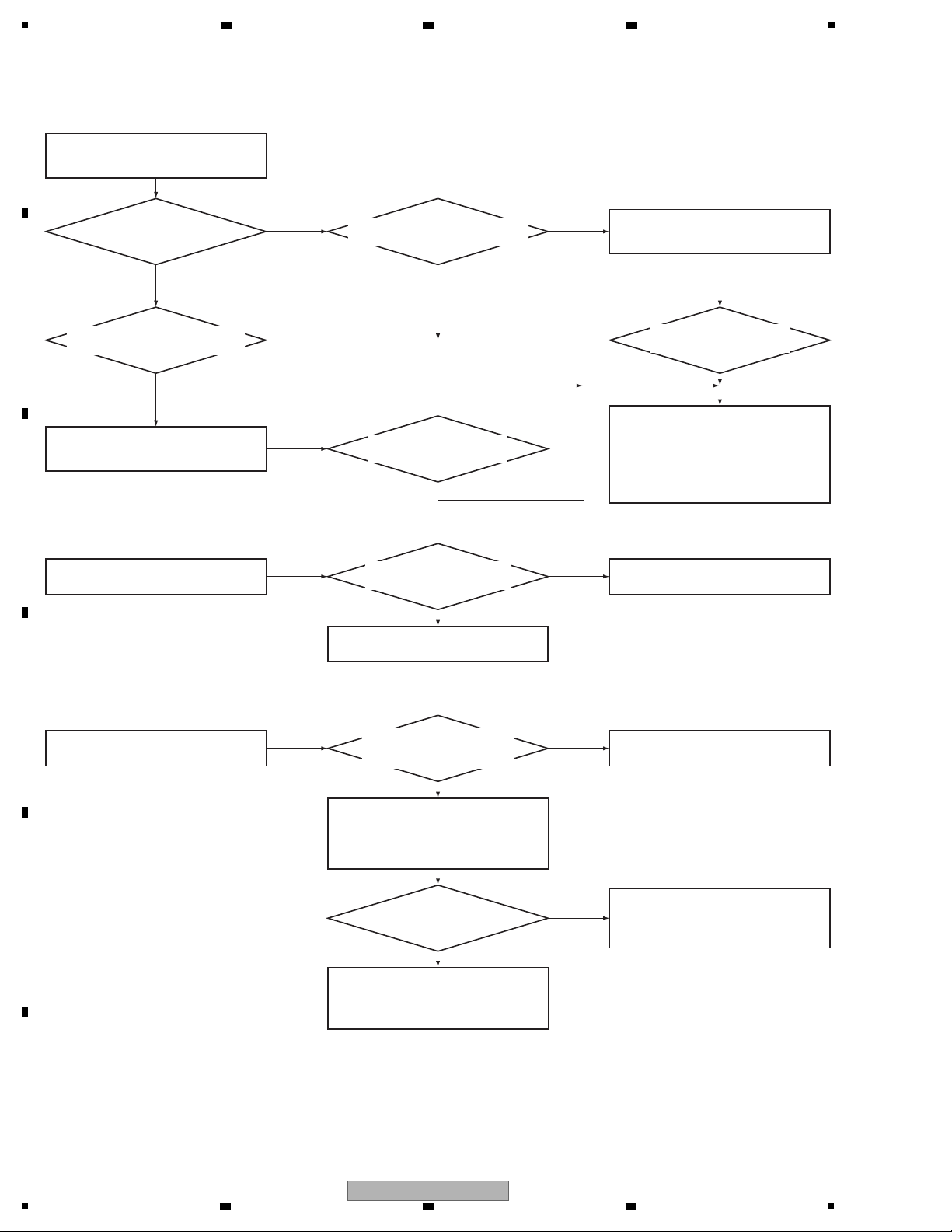
1
Check that the LAN settings of the main unit,
PC/Mac and CDJ Player are correct.
If rekordbox is not running, it can not connect
via LAN.
Check LAN HUB IC (IC2151), the peripheral
circuits of MAIN UCOM (IC701) and the power
supply. If no problem, replace the MAIN Assy.
Check that the LAN settings of the main unit,
PC/Mac and CDJ Player are correct.
If rekordbox is not running, it can not connect
via LAN.
Check LAN HUB IC (IC2151), the peripheral
circuits of MAIN UCOM (IC701) and the power
supply. If no problem, replace the MAIN Assy.
Ye s
PC/Mac is connected to EXTENSION
terminal of the main unit.
CDJ player is connected to CH3/CH4
terminals of the main unit.
No
Is the device to be connected
PC/Mac or CDJ player?
PC/Mac
Is PC/Mac connected to EXTENSION
terminal of the main unit?
Is PC/Mac connected to EXTENSION
terminal of the main unit?
Is the main unit connected to
the device via LAN possible?
Is the main unit connected to
the device via LAN possible?
CDJ player
Is CDJ player connected to CH3/CH4
terminals of the main unit?
Is CDJ player connected to CH3/CH4
terminals of the main unit?
Ye s
No
Is the main unit connected to
the device via LAN possible?
Is the main unit connected to
the device via LAN possible?
No
No
Confirm with peripheral device connected.
Confirmation of LAN
Confirmation of Browse LCD backlight
Connection between this unit and another
device via LAN is not possible. (This unit
cannot be recognized by rekordbox.)
The Browse LCD backlight does not light on.
Replace the LCD module.
Is the voltage of BL_A normal?
(Refer to "10.69 VOLTAGES")
Is the voltage of BL_A normal?
(Refer to "10.69 VOLTAGES")
Replace the MAIN Assy.
Normal
Abnormal
Confirmation of Browse LCD
Browse LCD is not displayed.
Browse LCD display is not normally.
See the section on "Startup is not completed"
when other than LCD is not working properly.
Is it operating normally except
the LCD? (Light on/off LED,
recognize USB or not etc...)
Is it operating normally except
the LCD? (Light on/off LED,
recognize USB or not etc...)
Is the voltage at each block normal?
No
Check it with removing the LCD module.
If the voltage changes normal, replace the
LCD module. If not improve, replace
LCDB Assy.
No
Ye s
See the section on "Confirmation of LCD backlight".
Check power supply to the LCD module.
Check the voltage at Pins 3, 4, 5 and 21 of
CN3603 in the LCDB Assy, referring to
"10.69 VOLTAGES."
Ye s
Replace MAIN Assy.
If the problem is not improve, replace
LCDB Assy. If it still not improve, replace
LCD module.
A
2 3 4
B
C
D
E
F
24
1
XDJ-XZ
2 3 4
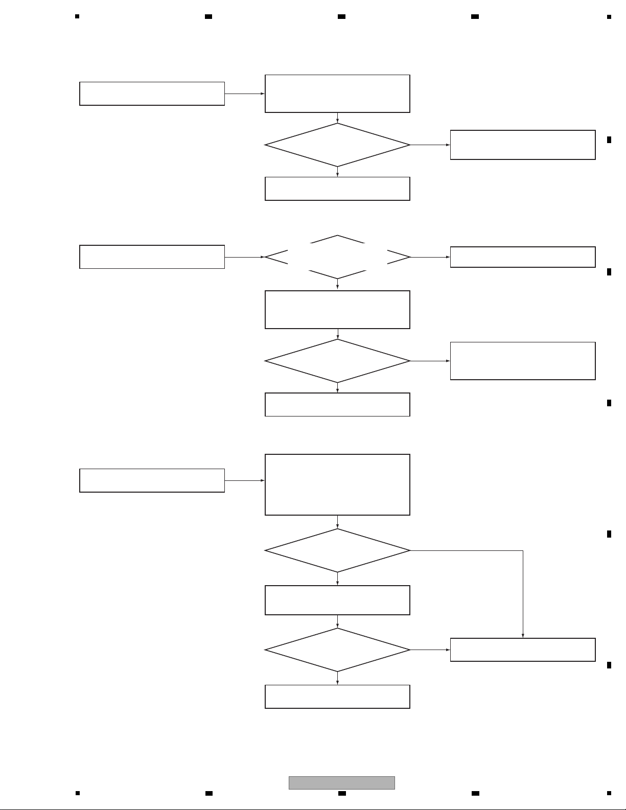
5
Confirmation of the Touch panel
Touch panel does not react.
Touch position of the Touch panel shifts.
Confirm Touch panel in Test mode.
When it can not be performed normally or
check in Test mode in case of NG, make the
following confirmation.
When operating the Touch panel, check
whether the waveform of Pins 1 to 4 of
CN3604 in LCDB Assy.
Check the communication route of TPNL_XINT,
TPNL_SCL/SDA (IC3606 d IC701).
Refer to "10. 70 WAVEFORMS" 2.
Replace LCDB Assy.
If not improve, replace the MAIN Assy.
As a problem in the Touch panel is
suspected, replace the Touch panel.
Does the waveform change?
No
Ye s
Will the waveform be output
when operating the touch panel?
Ye s
No
The JOG LCD backlight does not light on.
Replace JOG LCD module and JLCD1/2 Assy.
Check the voltage at Pin 2 of CN4503 and
at Pin 26 of CN4515 in the UCOM Assy,
referring to "10.69 VOLTAGES".
Confirmation of JOG LCD backlight
Ye s
Is the voltage normal?
Check the connection with MAIN Assy and
UCOM Assy, and the peripheral circuits of
IC502. If not improve, replace MAIN Assy.
No
The JOG LCD backlight does not light on.
Check the power supply of the JOG LCD module.
Check the voltage at Pin 9 of CN4503 and at
Pin 22 of CN4515 in the UCOM Assy,
referring to "10.69 VOLTAGES".
Confirmation of JOG LCD
Ye s
Ye s
Is it operating normally except
the LCD? (Light on/off LED,
recognize USB or not etc...)
Is it operating normally except
the LCD? (Light on/off LED,
recognize USB or not etc...)
Replace JLCD1/2 Assy.
If not improve, replace the JOG LCD module.
Is the voltage at each block normal?
Ye s
Check it with removing the JOG LCD module.
If the voltage changes normal, replace the
JOG LCD module. If not improve, replace
JLCD1/2 Assy.
No
See the section on "Startup is not completed"
when other than LCD is not working properly.
No
6 7 8
A
B
C
D
E
F
XDJ-XZ
5
6 7 8
25
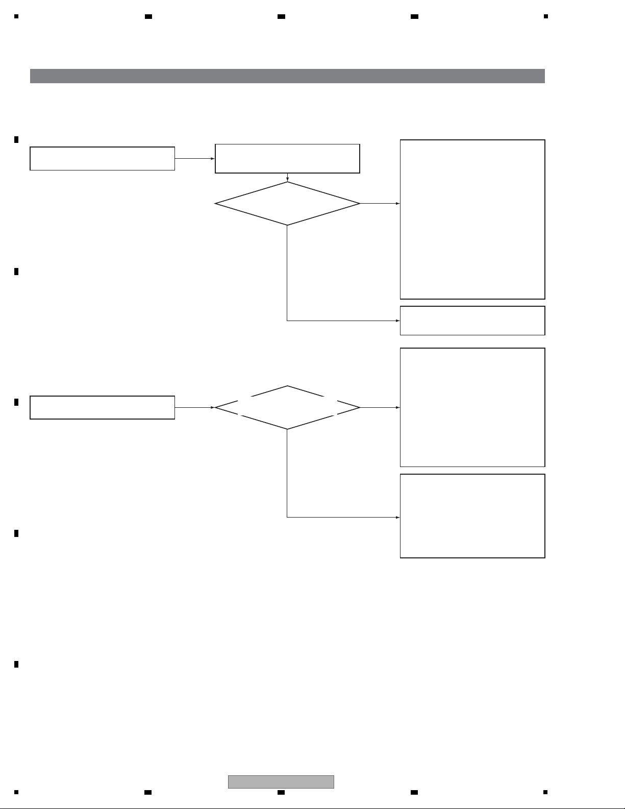
1
Trouble with the operating elements or LEDs
Some of the matrix keys (SW) do not function,
and some of the LEDs cannot light on.
[Confirmation work in advance]
Confirm whether LED / operation is OK.
Please refer to "6.1 TEST MODE" and confirm whether there are problems with LEDs/elements.
If there is a problem, please repair the defective part. (See "Display trouble", "Operation trouble".)
When making a diagnosis, refer also to "4.5 MATRIX INFORMATION" for diagnosis.
Check the corresponding grid, referring to
"4.5 MATRIX INFORMATION".
If no grid
waveform signal is output from the shift register
IC, check the communication line with the
microcomputer first, then check if the grid line is
short-circuited with GND, caused by a failure in
a key, LED, or the transistor for the drive.
Also check the connection of the grid line. If no
problem, replace the shift register IC:
! MIXER
block is in failure
MIXER Assy: Replace IC7004
! CDJ
block is in failure
DCK1 Assy: Replace IC8102
DCK2 Assy: Replace IC9003
! If Master level
indicator LEDs do not light on
DCK2 Assy: Replace IC9003 and IC9004
! If
CH level indicator LEDs do nor light on
MIXER Assy:
Replace IC7004, IC7005 and IC7006
Make sure that keys and LEDs that do not
work are using the same GRID in the
schematic diagram.
Is the same grid used?
Which key is not working
either direct key or matrix key?
Which key is not working
either direct key or matrix key?
Direct key
Matrix key
Ye s
No
No operation with keys (switches), No
operation with slide switches.
Check that current is conducted between the
terminals of the switch when it is pressed. If current
is not conducted, replace the switch. Check the line
between the switch and the microcomputer. If the
line is OK, replace the microcomputer to which the
switch is connected, as follows:
! ERP UCOM
UCOM Assy: Replace IC4502
! PANELM UCOM
UCOM Assy: Replace IC4505
! MAIN UCOM
Replace MAIN Assy
! JLCD1/JLCD2 Assy
Replace IC3002/IC3202
See "No operation with keys (switches), No
operation with slide switches" or "The LEDs
do not light."
Check the transistors on the line that is
connected to the microcomputer port and
waveforms and connections of the line. If no
problem, replace the microcomputer, as follows:
! ERP UCOM
UCOM Assy: Replace IC4502
! PANELM UCOM
UCOM Assy: Replace IC4505
! MIXER UCOM
MAIN Assy: Replace IC2302
A
2 3 4
B
C
D
E
F
26
1
2 3 4
XDJ-XZ
5
The rotary VRs are inoperable.
The rotary selector is inoperable.
Rotary selector:
Rotary selector, BEAT FX, BEAT FX CH, TIME
Rotation
Touch
JOG dial does not work.
Is it a rotation operation
that does not work?
Check that the resistance value of the line that is
connected to ground and the microcomputer
changes in accordance with turning of the VR.
Check the connection line between the
microcomputer and the VR. If no problem, replace
the microcomputers to which the VR is connected,
as follows:
! MAIN UCOM
Replace MAIN Assy
! ERP UCOM
UCOM Assy: Replace IC4502
! PANELM UCOM
UCOM Assy: Replace IC4505
Ye s
When push operation does not work, see
"No operation with keys (switches), No
operation with slide switches."
Ye s
When push operation does not work, see
"No operation with keys (switches), No
operation with slide switches."
The control microcomputer may be in failure,
replace it.
DCK1 side: IC3002
DCK2 side: IC3202
No
Check whether normal waveform is input to
the microcomputer referring to
"10.70 WAVEFORMS 1".
If normal waveform can not be confirmed,
replace it because it is probable that the
photo interrupter (PC9601/PC9701) is defective.
If no problem, replace the microcomputer.
DCK1 JOG control: IC3002
DCK2 JOG control: IC3202
No
Is it not a rotation operation
or a touch operation?
Does the Pins 1 of CN3003
/CN3203 (JOG_SW) become
0 V when touching JOG?
Does the Pins 1 of CN3003
/CN3203 (JOG_SW) become
0 V when touching JOG?
The slide VRs are inoperable.
TEMPO slider, Channel fader, Crossfader
Check if the voltage of the signal line changes
between 0 V and 3.3 V around 1.65 V. If it has
defective, replace the parts. If not improve,
check the parts on the signal line.
If no problem, replace the microcomputer.
! MAIN Assy: IC2302
6 7 8
A
B
C
D
E
F
XDJ-XZ
5
6 7 8
27
1
Do no LEDs connected to the
same grid light on?
Is there more than one
abnormal part?
Is the abnormal part direct LED?
Is the segment signal normal?
Do no LEDs controlled of the same
segment signals light on?
Do no LEDs controlled of the same
segment signals light on?
The LEDs do not light on.
Find the abnormal part in Test mode.
Replace the LED of the abnormal part.
Confirm the LED connection with the
microcomputer (IC4502/IC4503/IC701/IC3002/
IC3202) controlling the LED, and replace the
parts if there is any abnormality.
If no problem, replace the LED of the abnormal
part.
Check the LED connection with the
microcomputer (IC4502/IC4503/IC701/
IC3002/IC3202) controlling the LED.
If no problem, then replace the microcomputer.
Ye s
Check the corresponding grid, referring to
"4.5 MATRIX INFORMATION". And, check
the connection with the shift register or
microcomputer that controls the defective GRID.
If no problem, replace the shift register or
microcomputer.
! DCK1 Assy: Replace IC8102
! DCK2 Assy:
Replace IC9005, IC9003, IC9004
! MIXER Assy:
Replace IC7004, IC7005, IC7006
! PAD1/PAD2 Assy:
Replace IC4502, IC3901/IC4101,
IC3902/IC4102
! LCDB Assy:
Replace MAIN Assy
No
Replace the LED of the abnormal part.
No
Replace the LED of the abnormal part.
No
No
No
Ye s
Ye s
Ye s
Ye s
A
2 3 4
B
C
D
E
F
28
XDJ-XZ
1
2 3 4
5
Trouble in the audio system
No sound outputs from MASTER1/2.
Input the audio signal to the input terminal.
Or, playback via USB terminals.
Is signal output from neither
MASTER1 nor MASTER2?
Is the audio signal
interrupted around the muting
transistors in the AUDIO Assy?
Is the audio signal
interrupted around the muting
transistors in the AUDIO Assy?
Are there audio signals at
Pins 32, 33, 36, 37 (R-, R +, L-, L +)
of IC5802 of AUDIO Assy?
Are there audio signals at
Pins 32, 33, 36, 37 (R-, R +, L-, L +)
of IC5802 of AUDIO Assy?
Are there audio signals at Pin 6
(ADAT_M) of IC5802 of AUDIO Assy?
Are there audio signals at Pin 6
(ADAT_M) of IC5802 of AUDIO Assy?
Is MAS_MUTE
"H" (12 V)?
Muting is activated. The MUTE circuit in the
AUDIO Assy is in failure.
Replace the AUDIO Assy.
Check the periphery of Q6901/Q6904. If no
problem, replace the Q6901/Q6904.
If not improve, replace the AUDIO Assy.
Ye s
No data is input to the DAC (IC5802).
Check the connection between DSP (IC2501)
and DAC (IC5802).
If no problem, replace the MAIN Assy.
No
The muting transistors in the AUDIO Assy are
defective, which disables audio signal output.
Check the periphery of the muting transistors.
If no problem, then the muting transistors must
be replaced.
! AUDIO Assy:
Replace Q6014, Q6015, Q6016, Q6017
Ye s
No
No
No
Check for a point in the AUDIO Assy where
the audio signal is interrupted.
• If only MASTER 1 has no audio signal
output, check the periphery of IC4507/
IC4508. If no problem, then the OP
amplifiers must be replaced.
AUDIO Assy: Replace IC6001, IC6002
• If only MASTER2 has no audio signal
output, check the periphery of IC6003,
the capacitor or resistor is damaged or if
any circuit is open. If not improve, replace
AUDIO Assy.
No
No
The MASTER DAC (IC5802) is in failure.
Replace MASTER DAC (IC5802).
If not improve, replace the AUDIO Assy.
Ye s
Is MAS_VR_MUTE
"H" (3.3 V)?
Ye s
Ye s
Ye s
[Confirmation work in advance]
1 It discriminates defective area in the input and output
Refer to "5.3 SIMPLIFIED DIAGNOSTIC PROCEDURE FOR AUDIO SIGNAL", divide which of input and output has defects.
If all signal has defect, it has the defect on the power of audio, the clock of audio or the circuit near DSP.
2 It confirms whether there is a problem with the display or the operation.
Refer to "6.1 TEST MODE", it confirms whether there is a problem with the display or the operation.
If it has defect, repair the defective area. (Refer to flowchart about "Display trouble", "Operation trouble".)
[1] Error in output section
6 7 8
A
B
C
D
E
XDJ-XZ
5
6 7 8
F
29
1
Input the audio signal to the input terminal.
Or, playback via USB terminals.
Muting is activated. The MUTE circuit in the
AUDIO Assy is in failure.
Replace the AUDIO Assy.
Check for a point in the AUDIO Assy where
the audio signal is interrupted. And, replace it.
If not improve, replace AUDIO Assy.
No data is input to the DAC (IC5802).
Check the connection between DSP (IC2501)
and DAC (IC5802).
If no problem, replace the MAIN Assy.
Ye s
The MASTER DAC (IC5802) is in failure.
Replace MASTER DAC (IC5802).
If not improve, replace the AUDIO Assy.
Ye s
Is A_MUTE
"H" (12 V)?
Are there audio signals at
Pins 24, 25, 28, 29 (R-, R +, L-, L +)
of IC5802 of the AUDIO Assy?
Are there audio signals at
Pins 24, 25, 28, 29 (R-, R +, L-, L +)
of IC5802 of the AUDIO Assy?
Ye s
No
No
Are there audio signals at Pin 5 (ADAT_B)
of IC5802 of the AUDIO Assy?
Are there audio signals at Pin 5 (ADAT_B)
of IC5802 of the AUDIO Assy?
No
Is the audio signal
interrupted around the muting
transistors in the AUDIO Assy?
Is the audio signal
interrupted around the muting
transistors in the AUDIO Assy?
The muting transistors in the AUDIO Assy are
defective, which disables audio signal output.
Check the periphery of the muting transistors.
If no problem, then the muting transistors must
be replaced.
! AUDIO Assy: Repace Q6201-Q6208
Ye s
No
No sound outputs from BOOTH.
Ye s
No sound outputs from SEND.
Input the audio signal to the input terminal.
Or, playback via USB terminals.
Set the Beat FX channel setting to the
playback channel.
Muting is activated. The MUTE circuit in the
AUDIO Assy is in failure.
Replace the AUDIO Assy.
Ye s
Is A_MUTE
"H" (12 V)?
Check for a point in the AUDIO Assy where
the audio signal is interrupted. And, replace it.
If not improved, replace AUDIO Assy.
No data is input to the DAC (IC5802).
Check the connection between DSP (IC2501)
and DAC (IC5802).
If no problem, replace the MAIN Assy.
The MASTER DAC (IC5802) is in failure.
Replace MASTER DAC (IC5802).
If not improved, replace the AUDIO Assy.
Ye s
Are there audio signals at
Pins 38, 39, 42, 43 (R-, R +, L-, L +)
of IC5802 of the AUDIO Assy?
Are there audio signals at
Pins 38, 39, 42, 43 (R-, R +, L-, L +)
of IC5802 of the AUDIO Assy?
No
No
Are there audio signals at
Pin 7 (ADAT_S) of IC5802
of AUDIO Assy?
Are there audio signals at
Pin 7 (ADAT_S) of IC5802
of AUDIO Assy?
No
Is the audio signal
interrupted around the muting
transistors in the AUDIO Assy?
Is the audio signal
interrupted around the muting
transistors in the AUDIO Assy?
The muting transistors in the AUDIO Assy are
defective, which disables audio signal output.
Check the periphery of the muting transistors.
If no problem, then the muting transistors must
be replaced.
! AUDIO Assy: Replace Q6401, Q6402
Ye s
No
A
2 3 4
B
C
D
E
F
30
1
XDJ-XZ
2 3 4
 Loading...