

Page 1
ORDER NO.
RRV2381
STEREO CD/VCD TUNER
XC-NS3V
THIS MANUAL IS APPLICABLE TO THE FOLLOWING MODEL(S) AND TYPE(S).
Type
ZBDXJ DC power supplied from other system component
ZLXJ/NC DC power supplied from other system component
¶ This product is a system(s) component.
This product does not function properly independently ; to avoid malfunctions, be
sure to connect it to the prescribed system component(s), otherwise damage may
result.
¶ Please connect it to the STEREO POWER AMPLIFIER M-NS1, for adjustment and
operation inspection.
Model
XC-NS3V
Power Requirement Remarks
Component Model Service manual Remarks
STEREO CD/VCD TUNER XC-NS3V RRV2381 This manual.
STEREO POWER AMPLIFIER M-NS1 RRV2349 (RRV2321)
SPEAKER SYSTEM S-NS1-LRW RRV2371
MINIDISC RECORDER MJ-NS1 RRV2363
CONTENTS
1. SAFETY INFORMATION
2. EXPLODED VIEWS AND PARTS LIST
3. BLOCK DIAGRAM AND SCHEMATIC DIAGRAM
4. PCB CONNECTION DIAGRAM
5. PCB PARTS LIST
6. ADJUSTMENT
PIONEER CORPORATION 4-1, Meguro 1-chome, Meguro-ku, Tokyo 153-8654, Japan
PIONEER ELECTRONICS SERVICE, INC. P.O. Box 1760, Long Beach, CA 90801-1760, U.S.A.
PIONEER EUROPE NV Haven 1087, Keetberglaan 1, 9120 Melsele, Belgium
PIONEER ELECTRONICS ASIACENTRE PTE. LTD. 253 Alexandra Road, #04-01, Singapore 159936
c
PIONEER CORPORATION 2000
...............................................
....................................................
......................................
...............
.....
.........................
20
28
32
2
3
6
7. GENERAL INFORMATION
7.1 DIAGNOSIS
7.1.1 DISASSEMBLY
7.1.2 SINGLE OPERATION METHOD
7.2 PARTS
7.2.1 IC
7.2.2 DISPLAY
8. PANEL FACILITIES AND SPECIFICATIONS
..................................................
..........................................................
............................................................
.................................................
................................
......................................
............
T – ZZK SEPT. 2000 Printed in Japan
.......
35
35
35
38
39
39
53
54
Page 2
XC-NS3V
1. SAFETY INFORMATION
This service manual is intended for qualified service technicians ; it is not meant for the casual do-ityourselfer. Qualified technicians have the necessary test equipment and tools, and have been trained
to properly and safely repair complex products such as those covered by this manual.
Improperly performed repairs can adversely affect the safety and reliability of the product and may
void the warranty. If you are not qualified to perform the repair of this product properly and safely, you
should not risk trying to do so and refer the repair to a qualified service technician.
THE AEL(ACCESSIBLE EMISSION LEVEL) OF THE LASER POWER OUTPUT IS LESS THAN CLASS 1
BUT THE LASER COMPONENT IS CAPABLE OF EMITTING RADIATION EXCEEDING THE LIMIT FOR
CLASS1.
A SPECIALLY INSTRUCTED PERSON SHOULD DO SERVICING OPERATION OF THE APPARATUS.
LASER DIODE CHARACTERISTICS
MAXIMUM OUTPUT POWER: 5 mW
WAVELENGTH: 708- 785 nm
WARNING
LABEL CHECK
Additional Laser Caution
1. Laser Interlock Mechanism
The loading position detect switch (in CD mechanism
assembly) is set to "CLMP ON(CD CLOSE)" (ON:low
level,OFF:high level) position, the system control
IC(IC5501) get the "CLMP" signal, and hand the laser
"LDON" signal to IC1101.
Then a laser diode can be lighted except when the level of
signal CLMP is low.
The interlock also does not function in the test mode∗.
Laser diode oscillation will continue, if pin 9 of TA2150FN
(IC1101) on the SELF-CHUCK VCD ASSY is connected to
GND, or pin 10 is connected to low level (ON), or else the
terminals of Q1101 are shorted to each other (fault
condition).
2. When the cover is opened, close viewing of the objective
lens with the naked eye will cause exposure to a Class 1
laser beam.
∗ : Refer to page 32.
2
Page 3
2. EXPLODED VIEWS AND PARTS LIST
NOTES:• Parts marked by "NSP" are generally unavailable because they are not in our Master Spare Parts List.
2.1 PACKING
The mark found on some component parts indicates the importance of the safety factor of the part.
•
Therefore, when replacing, be sure to use parts of identical designation.
Screws adjacent to mark on the product are used for disassembly.
•
14
15
1
5
10
11
3
18
8
XC-NS3V
7
2
16 (1/2)
21
17
20
(1) PACKING PARTS LIST
Mark No. Description Part No.
1 Paper Pattern AAX7807
2 System Cable (20P) ADE7057
3 AC Power Cord See Contrast table (2)
4 FM Wire Antenna ADH7004
5 Operating Instructions ARE7267
(English/Chinese/Spanish)
6 AM Loop Antenna ATB7009
7 Ferrite Core ATX7007
8 Remote control Unit AXD7282
9 Battery Cover AZA7204
10 Stand A AXG7096
16 (2/2)
15
9
19
13
12
4
6
Mark No. Description Part No.
11 Stand B AXG7097
12 Video cord VDE1010
NSP 13 Batteries (R6P/AA) VEM-013
14 Polyethylene Bag Z21-013
(115 × 270 × 0.05)
NSP 15 Polyethylene Bag Z21-038
(0.03 × 230 × 340)
16 Rear Pad M AHA7296
17 Front Pad VCDR AHA7303
18 Spacer CD/VCD AHB7040
19 Spacer CDR AHB7048
20 Packing Case See Contrast table (2)
21 Sheet Z23-026
(2) CONTRAST TABLE
XC-NS3V/ZLXJ/NC and ZBDXJ are constructed the same except for the following :
Part No.
Mark No. Symbol and Description XC-NS3V XC-NS3V Remarks
/ZBDXJ /ZLXJ/NC
3 Power Cord ADG1158 ADG1154
20 Packing Case AHD7937 AHD7936
3
Page 4
XC-NS3V
2.2 EXTERIOR
49
62
E
52
32
C
60
69
69
2
E
69
34(1/2)
13
DB
30
73
68
DC
74
28
70
69
68
58
68
76
48
56
47(1/4)
47(3/4)
23
21
69
34(2/2)
69
69
37
56
11
69
75
I
E
53
50
69
9
55
D
69
69
33
7
F
69
35
69
43
24
36
69
27
K
3
18
B
A
17
69
44
71
69
46
4
J
42
A
41
38
69
19
26
2626
B
22
31(1/2)
69
40
39
A
15
57
58
69
D
47(2/4)
47(4/4)
H
6
G
69
69
69
8
69
69
DA
5
12
C
1
69
69
69
29
69
54
72
69
51
65
25
30
63
14
69
69
31(2/2)
45
59
16
10
69
B
20
61
C
69
69
64
72
25
66
ZBDXJ Only
4
Page 5

XC-NS3V
(1) EXTERIOR PARTS LIST
Mark No. Description Part No. Mark No. Description Part No.
1 MAIN UNIT AWU7600
2 DISP UNIT AWU7565
3 MOTOR UNIT AWU7566
4 CD SW UNIT AWU7567
5 AUX UNIT AWU7604
41 Slide Cam C ANW7200
42 Slide Cam D ANW7201
43 Gear N ANW7203
44 Gear Holder ANW7205
45 Shaft Assy AXG7102
6 KEY L UNIT AWU7569
7 LED UNIT AWU7570
8 KEY R UNIT AWU7625
9 SENSOR UNIT AWU7657
NSP 10 SELF-CHUCK VCD ASSY AWP7029
11 FM/AM TUNER MODULE AXQ7228
12 13P FFC/30V (J1) ADD7225
13 22P FFC/30V (J2) ADD7226
14 24P FFC/30V (J5) ADD7227
15 16P FFC/30V (J1101) ADD7245
16 CONNECTOR ASSY (J111) PF02PP2R05
17 Slider Motor VXM1033
18 CD Mecha KSM-770ABA
19 Float Spring ABH7191
NSP 20 Bottom Chassis VCD ANA7114
21 Door Angle AL2 ANG7332
22 Door Angle AR ANG7307
23 Door Angle BL2 ANG7333
24 Door Angle BR ANG7309
25 Leg AEB7090
26 Float Rubber AEB7129
27 Belt AEB7171
28 Push Rivet AEC7025
29 Barrier AEC7288
30 Chassis Sheet AEC7290
31 Mecha Holder AMR7311
32 FL Holder VCDR AMR7327
33 Reflector AMR7313
34 FFC Barrier AMR7314
35 Gear A ANW7063
46 Motor Pulley PNW1634
47 Button CD AAD7581
48 Door Window VA AAK7839
49 Door Window VB AAK7840
50 Sub Panel VCD AAK7786
51 Rear Cap VCD AAK7801
52 FL Window VCD AAK7861
53 Lens AAK7806
54 FL Cover VCDR AAK7800
55 Disc Lens AAK7847
56 Side Line AAP7074
57 Rear Line CD AAP7075
58 Screw ABA7061
59 Spacer AEB7061
60 FL Filter AEC7273
61 Bottom Base VCD AMA7023
62 Top Panel VCD AMB7720
NSP 63 Name Label See Contrast table (2)
64 Connector Label VCD ARW7120
65 Caution Label PRW1018
66 Label M See Contrast table (2)
67 • • • • • •
68 Screw BBZ30P080FMC
69 Screw BPZ30P080FZK
70 Screw BPZ30P120FMC
71 Screw PMZ26P040FMC
72 Screw VBZ30P100FZK
73 REG A UNIT AWU7655
74 REG B UNIT AWU7656
75 Side Panel VCD AAK7799
36 Gear Pulley A ANW7066
37 Cam Base L ANW7196
38 Cam Base R ANW7197
39 Slide Cam A ANW7198
40 Slide Cam B ANW7199
76 Rear Line VCDR AAP7079
(2) CONTRAST TABLE
XC-NS3V/ZLXJ/NC and ZBDXJ are constructed the same except for the following :
Part No.
Mark No. Symbol and Description XC-NS3V XC-NS3V Remarks
/ZBDXJ /ZLXJ/NC
NSP 63 Name Label AAL7265 AAL7264
66 Label M ARW7108 Not used
5
Page 6
1
23
XC-NS3V
3. BLOCK DIAGRAM AND SCHEMATIC DIAGRAM
3.1 BLOCK DIAGRAM
A
4
DA
AUX UNIT
(AWU7604)
IC1301
(M56788FP)
DRIVER
B
(TC9495F)
SELF-CHUCK
VCD ASSY
IC1201
SERVO
DSP
D/A
85 9 89 8
38
25
RF AMP.
Q1101
9
IC1101
(TA2150FN)
VCD5
(AWP7029)
B
3
FUNCTION
SW
15
7
IC3502
(BA4558F)
BALANCED
BUFFER(+)
5
7
IC3503
(BA4558F)
BALANCED
BUFFER(-)
C
13
5
C
14
12
11
IC3501
(BU4052BCF)
C 1/2, C 2/2
BALANCED
IC3504
(BA4558F)
1
CD MUTE
Q3503
AMP
MAIN UNIT (AWU7600)
V+12
V+9
V-9
VE+5BU
VE+5
Q5501
D5503
D
IC503 IC504
DB
+5V Reg. -5V Reg.
REG A UNIT
(AWU7655)
V+10
Q501
V+9
V-9
V+5
REG B UNIT
(AWU7656)
FLAC
IC551
Q551, Q552
D551-D556
VOLTAGE SUPPLY
for FL
V-5
DC
V-40
FM/AM
A
TUNER MODULE
(AXQ7228)
6
1234
Page 7
5
678
XC-NS3V
Note : When ordering service parts, be sure to refer to "EXPLODED VIEWS and PARTS LIST" or "PCB PARTS LIST".
MOTOR UNIT
K
(AWU7566)
A
MPEG
DECODER
67
4 110
IC1701
(CL680T-D1)
4M
DRAM
IC1756
(MSM514260C-60TS)
VCD
U-COM
IC1501
(PDC065A)
DISP UNIT
E
(AWU7565)
X5901
(GP1U27X)
INFRARED
SENSOR
G
KEY R UNIT
(AWU7625)
DOOR OPEN CODE
KEY L UNIT
H
(AWU7569)
I
SENSOR UNIT
(AWU7657)
D5912
(SIR-56ST3F)
B
(PDA5601A)
(AAV7077)
(MSM9202-01)
5
IC5652
FL
V5651
FL
DRIVER
IC5651
F
LED UNIT
(AWU7570)
6
CD SW UNIT
J
(AWU7567)
7
C
D
7
8
Page 8
1
XC-NS3V
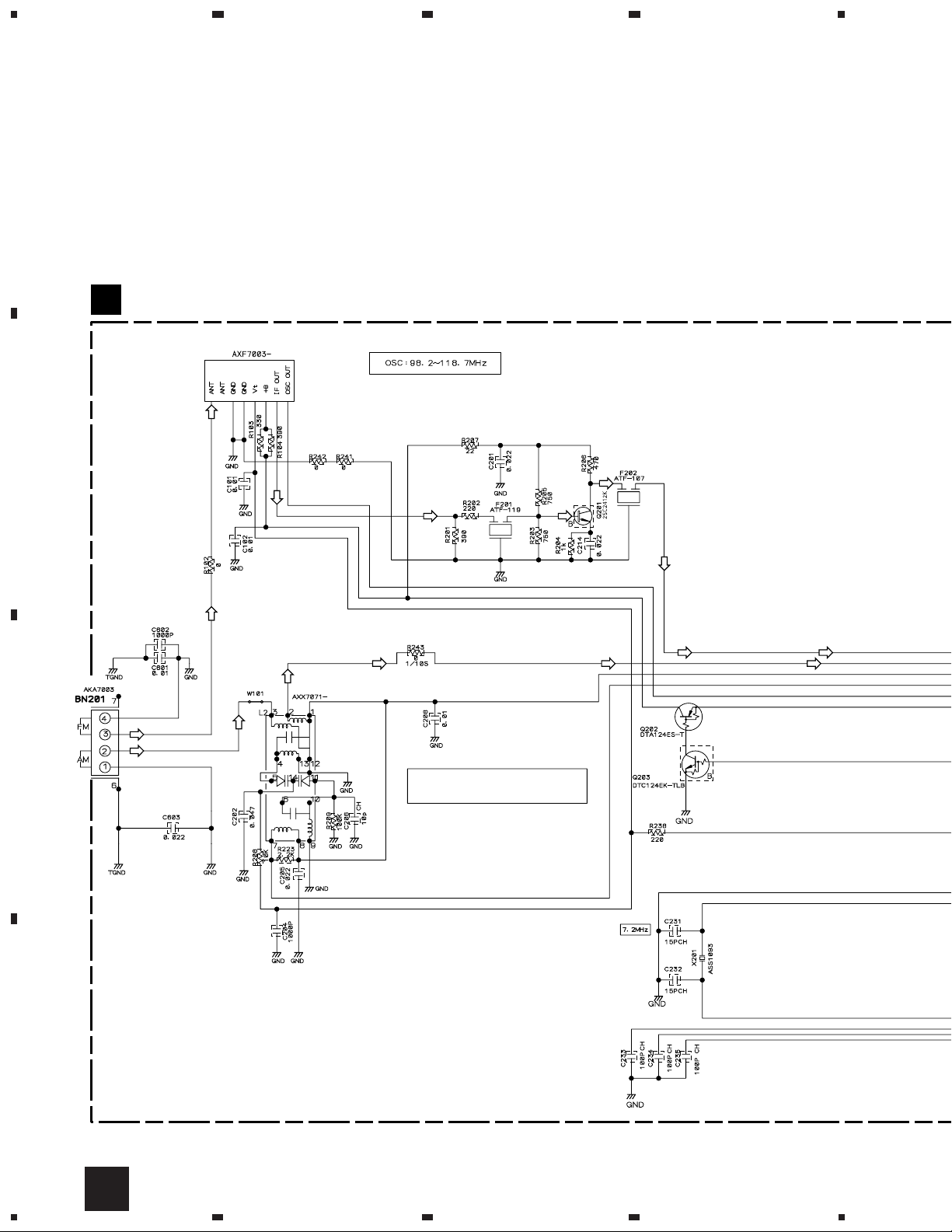
3.2 FM/AM TUNER MODULE
A
FM/AM TUNER MODULE (AXQ7228)
A
FM FRONT END
23
4
B
(FM)
(FM)
(FM) (FM)
(AM) (AM)
MW RF TUNING BLOCK
(AM)
(FM)
C
(AM)
(AM)
OSC : 981 - 2052kHz 9k step
(FM)
(FM)
(FM)
(FM) (FM)
(AM)
D
8
A
1234
Page 9
5
678
XC-NS3V
A
: The power supply is shown with the marked box.
(TX)
: AUDIO SIGNAL ROUTE (TUNER)
(AM)
: AM SIGNAL ROUTE
(FM)
: FM SIGNAL ROUTE
(AM)
(FM)
(AM)
(AM)
(AM)
(AM)
AM/FM IF+MPX IC
(FM)
(AM)
(AM)
(FM)
(AM)
L201
ATE7003
(AM)
(TX)
(FM)
(TX)
(TX)
(TX)
(TX)
B
CN1
1/2
C
C
PLL IC
D
A
5
6
7
8
9
Page 10
1
23
XC-NS3V
3.3 SELF-CHUCK CD ASSY (1/2)
4
A
B
B 1/2
SELF-CHUCK VCD ASSY
(AWP7029)
(CD)
(CD)
(CD)
C
D
10
1/2
B
1234
Page 11
5
678
XC-NS3V
: The power supply is shown with the marked box.
SIGNAL ROUTE
(CD)
: CD AUDIO SIGNAL ROUTE
(D)
: DIGITAL SIGNAL ROUTE
: VIDEO SIGNAL ROUTE
4.89V
3.35V
3.3V REG
CN1201
A
B
B 2/2
(CD)
(D)(D)
CN1203
CN5
C 1/2
C
D
1/2
5
6
7
B
8
11
Page 12
1
XC-NS3V
3.4 SELF-CHUCK VCD ASSY (2/2)
A
23
6.7V
4
(FS)
(FS)
(TS)
(FS)
(FS)
(TS)
(TS)
B
(TS)
(TS)
(FS)
(FS)
(SM)
(CM)
(LM)
(CM)
(LM)
(SM)
(CM)
(LM)
(LM)
(SM)
(CM)
(CM)
(SM)
(SM)
(SM)
(RF)
(CM)
(FS)
(TS)
(FS)
(TS)
SELF-CHUCK VCD ASSY
B 2/2
CN1302
CN111
(LM)
(LM)
K
C
CN1301
(CM)
(CM)
Note: The encircled numbers denote measuring point in the schematic diagram.
1
(AWP7029)
IC1101- Pin 25:
PLAY MODE (RF)
H : 500nsec/div
1.0Vp-p
VC
IC1101- Pin 14:
2
TEST MODE,
Tracking Open (TRER)
H : 5msec/div
VC : IC1101- Pin19
2.0Vp-p
VC
(TS)
(FS)
(CM)
(SM)
(TS)
(SM)
To. VCD MECHA
(SM)
CN1101
(FS)
(TS)
(TS)
(FS)
1
4.25V
D
To. P.U Assy
12
B
2/2
(TS) (TS)
VC
2
2.15V
(FS)
1234
(FS)
(FS)
Page 13
5
678
XC-NS3V
A
(D)
(CD)
(D)
B
(TS)
(FS)
(TS)
(FS)
(CM)
(SM)
(TS)
(CM)
(SM)
(CD)
(CD)
2.44V
(CD)
B 1/2
C
SIGNAL ROUTE
(CD)
: CD AUDIO SIGNAL ROUTE
(D)
: DIGITAL SIGNAL ROUTE
: RF SIGNAL ROUTE
(FS)
: FOCUS SERVO LOOP LINE
(TS)
: TRACKING SERVO LOOP LINE
5
(SM)
: SPINDLE MOTOR ROUTE
(CM)
: CARRIAGE MOTOR ROUTE
(LM)
: LOADING MOTOR ROUTE
: The power supply is shown with the marked box.
6
(CD)
(CD)
D
2/2
7
B
8
13
Page 14
1
23
XC-NS3V
3.5 MAIN (1/2), AUX, REG A and REG B UNITS
(A)
A
B 1/2
4
CN1201
(A)
(A)
DA
AUX UNIT
(AWU7604)
B
(PB)
(PB)
(REC)
(REC)
(A)
(PB)
(PB)
(A)
(TX)
(REC)
(REC)
+4.0V
-4.0V
C
(TX)
(TX)
From M-NS1 T0 MJ-NS1
+11.2V
C 2/2
A
(TX)
CN201
D
CN102
E
14
1/2
C
1234
DA DB DC
Page 15
5
678
XC-NS3V
C 1/2
MAIN UNIT (AWU7600)
A
B
DB
REG A UNIT
(AWU7655)
PDC073A
SYSTEM CONTROL
MICROCOMPUTER
C
DC
REG B UNIT
(AWU7656)
: The power supply is shown with the marked box.
: AUDIO SIGNAL ROUTE
(TX)
: TUNER AUDIO SIGNAL ROUTE
(A)
: AUX AUDIO SIGNAL ROUTE
5
(REC)
: REC AUDIO SIGNAL ROUTE
(PB)
: PB AUDIO SIGNAL ROUTE
6
D
1/2
C
7
8
15
Page 16
1
XC-NS3V
3.6 MAIN (2/2) UNIT
A
C 1/2
B
23
C 2/2
MAIN UNIT (AWU7600)
+8.9V
4
-8.9V
C
D
16
2/2
C
1234
Page 17
5
678
XC-NS3V
A
B
: The power supply is shown with the marked box.
C
D
2/2
C
5
6
7
8
17
Page 18
1
23
XC-NS3V
3.7 DISP, LED, KEY R, KEY L, SENSOR, CD SW and MOTOR UNITS
4
A
-35.0V
B
+4.75V
-30V
+2.75V
C
MICROCOMPUTER
DISP UNIT
E
D
(AWU7565)
18
CN2
C 1/2
E
1234
Page 19

5
678
XC-NS3V
A
G
KEY R
UNIT
(AWU7625)
LED UNIT
(AWU7570)
F
KEY L
H
UNIT
(AWU7569)
J
K
CD SW UNIT
(AWU7567)
MOTOR UNIT
(AWU7566)
I
SENSOR
UNIT
(AWU7657)
KEY R UNIT
S5904 : 7 (STOP)
S5905 : 6
(PLAY/PAUSE)
S5906 : OPEN/CLOSE
KEY L UNIT
S5901 : STANDBY/ON
S5902 : VOL. S5903 : VOL. +
CN1302
B 2/2
B
C
: The power supply is shown with the marked box.
5
6
D
J KH IF GE
7
8
19
Page 20

XC-NS3V
4. PCB CONNECTION DIAGRAM
NOTE FOR PCB DIAGRAMS :
1. Part numbers in PCB diagrams match those in the schematic
diagrams.
2. A comparison between the main parts of PCB and schematic
diagrams is shown below.
Symbol In PCB
Diagrams
BCE
BCE
D
Symbol In Schematic
Diagrams
BCEBCE
BCE
DGGSS
BCE
DGS
Part Name
Transistor
Transistor
with resistor
Field effect
transistor
Resistor array
3. The parts mounted on this PCB include all necessary parts for
several destinations.
For further information for respective destinations, be sure to
check with the schematic diagram.
4. View point of PCB diagrams.
Connector
Capacitor
SIDE A
P.C.Board
Chip Part
SIDE B
3-terminal
regulator
20
Page 21

1
4.1 FM/AM TUNER MODULE
234
XC-NS3V
A
FM/AM TUNER MODULE
SIDE A
A
B
A
FM/AM TUNER MODULE
C
Q202
CN1
(ANP7338-B)
SIDE B
C
D
Q201
1
2
IC201 Q205
3
Q203
IC202
(ANP7338-B)
Q204
A
4
21
Page 22

1
23
XC-NS3V
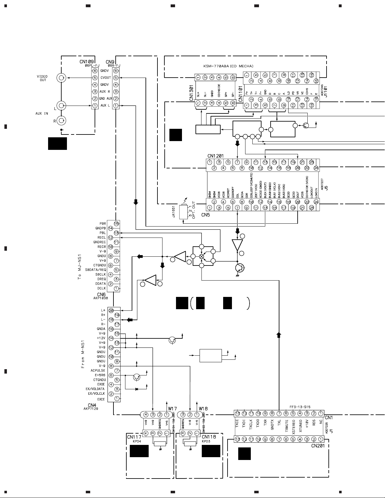
4.2 MAIN, AUX, REG A and REG B UNITS
4
MAIN UNIT
A
IC501
IC502
C
DA
DB
REG A UNIT
B
IC551
AUX UNIT
(ANP7346-C)
DC
REG B UNIT
A
Q551
Q552
CN201
(ANP7346-C)
Q3502
IC3501
IC3502
IC3504
IC3503
C
IC5701
E
CN102
IC5501
Q5502
Q5505
B
CN1201
D
22
SIDE A
(ANP7346-C)
M-NS1
C
DA DB DC
1234
MJ-NS1
Page 23

1
234
XC-NS3V
AUX UNIT
DA
(ANP7346-C)
DC
REG B UNIT
(ANP7346-C)
DB
REG A UNIT
MAIN UNIT
C
A
Q501
IC551
B
SIDE B
(ANP7346-C)
Q3501
Q3503
Q4001
Q3504
Q4002
IC5501
Q5504
Q5501
Q5503
C
D
C
1
2
DA DB DC
3
4
23
Page 24

1
23
XC-NS3V
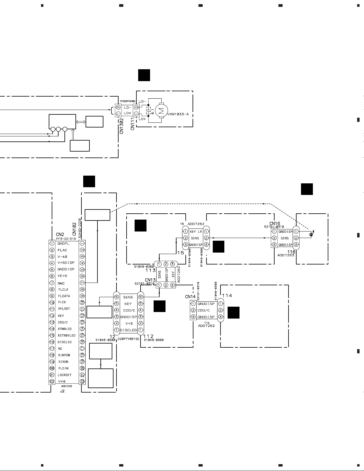
4.3 DISP, LED, KEYR, KEYL, SENSOR and CD SW UNITS
DISP UNIT
A
E
SIDE A
(ANP7346-C)
B
4
IC5651
Q5652
Q5912
Q5903
IC5652
Q5913
Q5911
Q5910
Q5908
LED UNIT
F
C
CN2
CD SW UNIT
C
SENSOR UNIT
I
J
KEY L UNIT
H
D
24
E
1234
G H IF J
KEY R UNIT
G
Page 25

1
DISP UNIT
E
234
XC-NS3V
A
Q5907
Q5906
Q5905
Q5651
IC5651
SIDE B
(ANP7346-C)
Q5652
B
Q5653
CD SW UNIT
J
LED UNIT
F
SENSOR UNIT
I
Q5909
C
KEY R UNIT
G
1
KEY L UNIT
H
D
E G H IF
2
3
J
4
25
Page 26

1
23
XC-NS3V
4.4 SELF-CHUCK VCD ASSY and MOTOR UNIT
A
SELF-CHUCK VCD ASSY
B
IC1751
IC1776
IC1771
Q1302
B
4
IC1301
IC1001
Q1101
CD MECHA
C
(ANP7359-C)
MOTOR UNIT
K
SIDE A
B
CN1302
D
(ANP7346-C)
26
B
K
1234
Page 27

1
SELF-CHUCK VCD ASSY
B
234
XC-NS3V
Q1741
IC1756
IC1701
A
B
K
CN111
CD MECHA
C
CN5
(ANP7359-C)
SIDE B
MOTOR UNIT
K
IC1202
IC1201
IC1101
Q1102
IC1501
C
D
(ANP7346-C)
B K
1
2
3
4
27
Page 28

XC-NS3V
Mark No. Description Part No. Mark No. Description Part No.
5. PCB PARTS LIST
NOTES:•The mark found on some component parts indicates the importance of the safety factor of the part.
Therefore, when replacing, be sure to use parts of identical designation.
When ordering resistors, first convert resistance values into code form as shown in the following examples.
•
Ex.1 When there are 2 effective digits (any digit apart from 0), such as 560 ohm and 47k ohm (tolerance is shown by J=5%,
and K=10%).
560 Ω→56 × 10
47k Ω→47 × 10
0.5 Ω→R50 ..................................................................................... RN2H
1
→ 561 ........................................................ RD1/4PU 5 6 1 J
3
→ 473 ........................................................ RD1/4PU 4 7 3 J
R 5 0
K
1 Ω→1R0 ..................................................................................... RS1P 1 R 0 K
Ex.2 When there are 3 effective digits (such as in high precision metal film resistors).
5.62k Ω→ 562 × 10
1
→ 5621 ......................................................RN1/4PC 5 6 2 1 F
Mark No. Description Part No.
LIST OF PCB ASSEMBLIES
FM/AM TUNER MODULE AXQ7228
SELF-CHUCK VCD ASSY AWP7029
CD TX MAIN ASSY AWM7517
DISP UNIT AWU7565
MOTOR UNIT AWU7566
CD SW UNIT AWU7567
KEY L UNIT AWU7569
LED UNIT AWU7570
MAIN UNIT AWU7600
AUX UNIT AWU7604
KEY R UNIT AWU7625
REG A UNIT AWU7655
REG B UNIT AWU7656
SENSOR UNIT AWU7657
FM/AM TUNER MODULE
A
SEMICONDUCTORS
IC201 BA1451F
IC202 LC72131MD
Q201, Q204, Q205 2SC2412K
Q202 DTA124ES
Q203 DTC124EK
D201 1SS133
D202 MTZJ5.1C
COILS AND FILTERS
L201 FM DETECTOR COIL ATE7003
F202 CERAMIC FILTER ATF-107
F201 CERAMIC FILTER ATF-119
F203 AM CERAMIC FILTER ATF1155
Mark No. Description Part No.
C228 CEAT3R3M50
C237 CEAT470M10
C211 CEJA1R0M50
C210 CEJA470M16
C204, C238, C602 CKSRYB102K50
C101, C102, C208, C220, C239 CKSRYB103K50
C242, C601 CKSRYB103K50
C216, C217 CKSRYB123K50
C225 CKSRYB153K50
C201, C205, C209, C214, C230 CKSRYB223K50
C236, C603 CKSRYB223K50
C221 CKSRYB224K10
C202, C222 CKSRYB473K16
C215 CKSRYB681K50
RESISTORS
R211 RD1/4PU221J
R221 RD1/4PU222J
R233 RD1/4PU391J
R243 RS1/10S0R0J
R103 RS1/10S331J
R104 RS1/10S391J
Other Resistors RS1/16S&&&J
OTHERS
CN201 13P CONNECTOR 52044-1345
BN201 TERMINAL 4P AKA7003
SHIELD CASE T ANK7072
SHIELD CASE B ANK7073
X201 CRYSTAL RESONATOR ASS1093
(7.2000 MHz)
FM FRONT END AXF7003
AM RF TUNING BLOCK AXX7071
CAPACITORS
C206 CCSRCH100D50
C212, C213, C226, C233–C235 CCSRCH101J50
C240 CCSRCH101J50
C231, C232 CCSRCH150J50
C223 CEAT100M50
C229 CEAT101M10
C224 CEAT1R0M50
C227 CEAT220M25
C241 CEAT2R2M50
C243 CEAT330M16
28
SELF-CHUCK VCD ASSY
B
SEMICONDUCTORS
IC1001 BA033FP
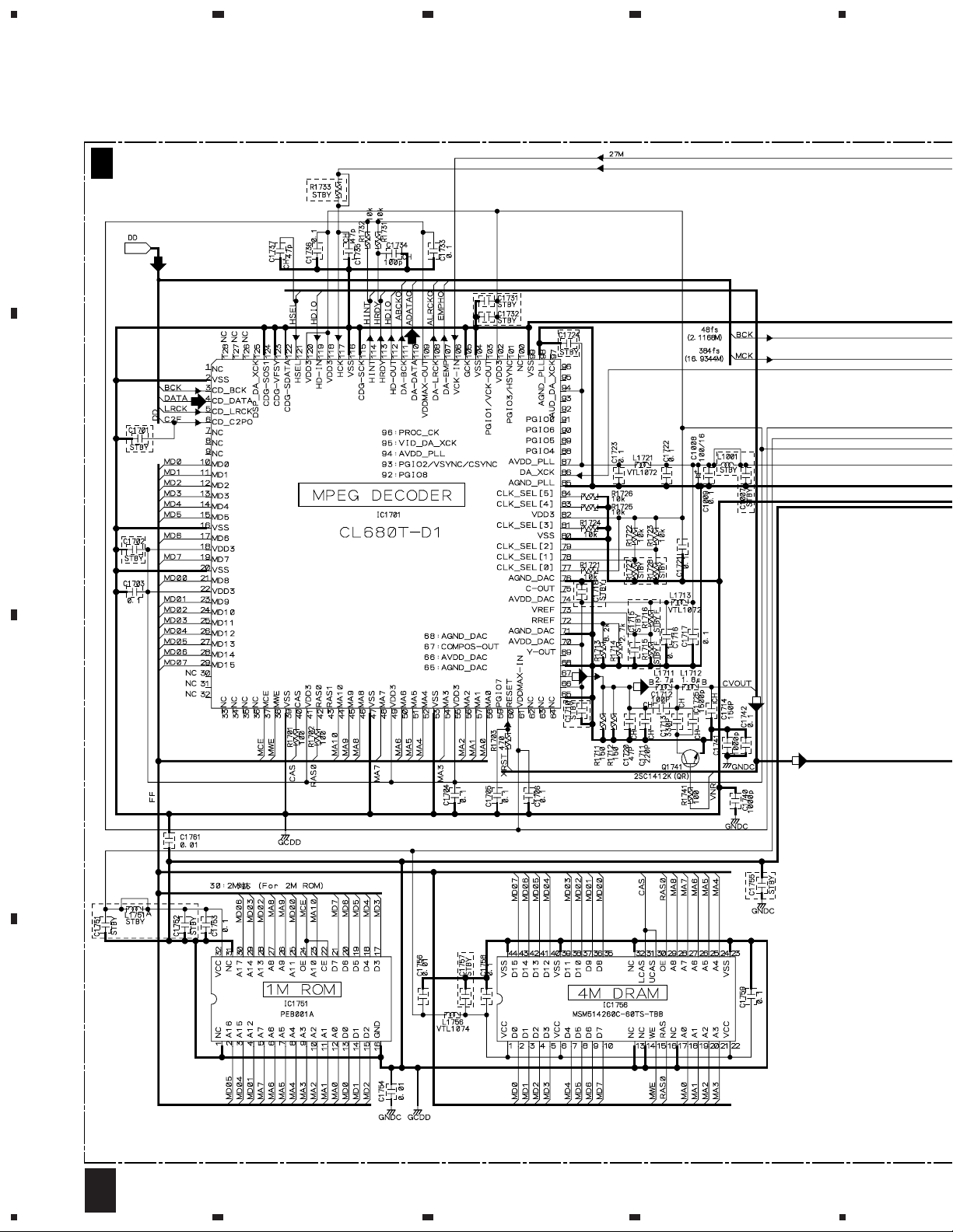
IC1701 CL680T-D1
IC1301 M56788FP
IC1756
IC1751 PEB001A
IC1101 TA2150FN
IC1202 TC74HC32AF
IC1776 TC7W14FU
IC1771 TC7WU04FU
IC1201 TC9495F
MSM514260C-60TS
Page 29

XC-NS3V
Mark No. Description Part No. Mark No. Description Part No.
Q1101 2SA1036K
Q1302 2SA1037K
Q1741 2SC2412K
Q1102 DTC124TKA
D1301 UDZ2.0B
COILS AND FILTERS
L1302 LCTB1R8K1608
L1712 LCTB1R8K2125
L1711 LCTB2R7K2125
L1102, L1202, L1206 QTL1013
CHIP SOLID INDUCTOR
L1713, L1721 CHIP BEADS VTL1072
L1756 CHIP BEADS VTL1074
L1777 CHIP BEADS VTL1086
L1771, L1776 CHIP BEADS VTL1087
L1210 CHIP BEADS VTL1089
L1209 CHIP BEADS VTL1110
CAPACITORS
C1119, C1126, C1712, C1734 CCSRCH101J50
C1773, C1774 CCSRCH120J50
C1201 CCSRCH150J50
C1307, C1714 CCSRCH151J50
C1117, C1202, C1209 CCSRCH220J50
C1711 CCSRCH221J50
C1118 CCSRCH330J50
C1713 CCSRCH331J50
C1210, C1303, C1720, C1735, C1737 CCSRCH470J50
C1116 CCSRCK2R0C50
C1008, C1101, C1102, C1108, C1205 CEV101M16
C1222, C1224, C1231, C1328, C1501 CEV101M16
C1115, C1236 CEV101M4
C1001, C1003, C1203, C1228 CEV470M6R3
C1005, C1011, C1132, C1240, C1242 CKSRYB102K50
C1249, C1250, C1512, C1740, C1741 CKSRYB102K50
C1771, C1776 CKSRYB102K50
C1002, C1004, C1103, C1107, C1114 CKSRYB103K50
C1130, C1204, C1206, C1207, C1212 CKSRYB103K50
C1214, C1223, C1225–C1227, C1230 CKSRYB103K50
C1232, C1239, C1259, C1315, C1316 CKSRYB103K50
C1502, C1503, C1506, C1754, C1756 CKSRYB103K50
C1761 CKSRYB103K50
C1006, C1009, C1012, C1104 CKSRYB104K16
C1110, C1111, C1131, C1245, C1261 CKSRYB104K16
C1322, C1325, C1350, C1511 CKSRYB104K16
C1703–C1706, C1716, C1717 CKSRYB104K16
C1721–C1723, C1733, C1736, C1742 CKSRYB104K16
C1753, C1758, C1759, C1772, C1777 CKSRYB104K16
C1725 CKSRYB152K50
C1211 CKSRYB153K25
C1213 CKSRYB222K50
C1112, C1113 CKSRYB224K10
C1215 CKSRYB333K16
C1237, C1291 CKSRYB471K50
C1216, C1217 CKSRYB473K16
C1311, C1319 CKSRYB682K50
RESISTORS
R1112, R1522 (47kΩ) ACN7077
R1219, R1513 (220Ω) DCN1093
R1117, R1534 (10kΩ) DCN1094
R1318 RS1/16S1202F
R1319 RS1/16S2202F
OTHERS
SEMICONDUCTORS
COILS AND FILTERS
CAPACITORS
R1317 RS1/16S2702F
Other Resistors RS1/16S&&&J
CN1203 6P CONNECTOR RKN1047
CN1101 16P CONNECTOR RKN1057
CN1201 24P CONNECTOR RKN1065
CN1302 CONNECTOR S2B-PH-SM3
CN1301 CONNECTOR S6B-PH-SM3
X1201 CRYSTAL RESONATOR VSS1084
X1751 CRYSTAL RESONATOR VSS1086
X1501 CERAMIC RESONATOR VSS1115
MAIN UNIT
C
IC3502–IC3504 BA4558F-HT
IC3501 BU4052BCF
IC551 BU4069UB
IC5501 PDC073A
Q4001 2SB1132
Q552 2SB1237X
Q3501–Q3504, Q501, Q5501, Q5504 2SC2412K
Q551 2SD1858X
Q3505 DTA124EK
Q5502, Q5505 DTC124EK
Q4002, Q5503 DTC143EK
D505–D507, D551–D556 1SR154-400
D1654, D3501, D3551–D3553 1SS355
D5503, D5504, D5506 1SS355
D3503–D3506, D503 UDZ11B
D559 UDZ15B
D5501, D5505 UDZS6.8B
L1651, L5501 LFEA220J
L551, L552 LFEA680J
C5507 ACH1246
C5513, C5521–C5524, C5533 CCSQCH101J50
C5535, C5536 CCSQCH101J50
C3558 CCSQCH331J50
C563–C565 CCSQSL391J50
C3513, C3514, C3519, C3520 CCSRCH101J50
C5511, C5512, C5528, C5534 CCSRCH101J50
C559, C566 CEAL101M10
C508, C556, C558, C560 CEAL470M16
C552, C554, C555, C557, C571 CEAL470M25
C553 CEAL470M35
C5501 CEAT100M50
C1651, C501, C502, C505, C506 CEAT101M10
C5506, C5509 CEAT101M10
C5504 CEATR10M50
C3511, C3512 CEJQ101M10
C3523, C3524, C3535, C3536 CEJQ220M10
C3521, C3522 CEJQ2R2M50
C1652, C1653, C3509, C3510, C509 CKSQYB103K50
C5502 CKSQYB103K50
(16.9MHz)
(27.0MHZ)
(10MHZ)
29
Page 30

XC-NS3V
Mark No. Description Part No. Mark No. Description Part No.
C5519, C5520, C5525–C5527 CKSQYB152K50
C551, C561, C562, C567 CKSQYB473K50
C3557, C5503, C5505, C5508 CKSQYF104Z25
C569, C570 CKSQYF104Z25
C3537, C3538 CKSQYF105Z16
C5517, C5518 CKSRYB103K50
C5510, C5530 CKSRYF104Z25
RESISTORS
All Resistors RS1/10S&&&J
OTHERS
CN109 CONNECTOR 6P 06PL-FJ
JA3502 3P RCA PINJACK AKB7053
RESISTORS
R5573, R5574, R5576 RS1/10S1002F
R5588 RS1/16S5602F
R3521, R3522, R3547, R3548 RS1/10S4701F
R3549–R3551, R3553, R3554 RS1/10S5101F
R3555, R3563, R5592–R5595 RS1/16S0R0J
R3527, R3528 RS1/16S101J
R5584 RS1/16S102J
R3505, R3506 RS1/16S103J
R3537, R3538, R3562, R5578, R5585 RS1/16S104J
R3507, R3508 RS1/16S123J
R3556, R3559 RS1/16S181J
R5583 RS1/16S182J
R3541, R3542, R5552, R5553, R5555 RS1/16S222J
R5558 RS1/16S223J
R5579 RS1/16S333J
R3519, R3520 RS1/16S4701F
R3525, R3526 RS1/16S470J
R5512, R5513, R5538, R5548, R5549 RS1/16S471J
R3543, R3544 RS1/16S472J
R5577, R5580 RS1/16S473J
R3552 RS1/16S5101F
R5524–R5526, R5532–R5536 RS1/16S563J
R5557 RS1/16S822J
Other Resistors RS1/10S&&&J
OTHERS
CN9 CONNECTOR 4P 06R-FJ
CN6 SOCKET(15P) AKP1038
CN4 20P SOCKET AKP7129
1 SHIELD CASE ANK7082
1651 BUZZER APV7002
J18 JUMPER WIRE D25PWY0305E
J17 JUMPER WIRE D25PWY0415E
CN1 13P CONNECTOR FF3-13-S15
CN2 22P CONNECTOR FF3-22-S15
JA1651 OPTICAL LINK OUT GP1FA550TZ
CN5 24P CONNECTOR VKN1428
KN1 EARTH METAL FITTING VNF1084
X5501 CERAMIC RESONATOR DSS1048
AUX UNIT
DA
(10MHz)
COILS AND FILTERS
L3501 VTL1099
CAPACITORS
C3545 CCSQCH121J50
C3501–C3504 CCSQSL331J50
C3543 CEAT471M6R3
C3542 CKSQYB102K50
C3546 CKSQYF104Z25
REG A UNIT
DB
SEMICONDUCTORS
IC503 NJM7805FA
CAPACITORS
C513 CEAT100M50
C511 CKSQYF105Z16
OTHERS
CN117 4PJUMPERCONNECTOR KPD4
REG B UNIT
DC
SEMICONDUCTORS
IC504 NJM7905FA
CAPACITORS
C514 CEAT100M50
C512 CKSQYF105Z16
OTHERS
CN118 3PJUMPERCONNECTOR KPD3
DISP UNIT
E
SEMICONDUCTORS
IC5651 MSM9202-01
IC5652 PD5601A
Q5910 2SA1037K
Q5652 2SB1238X
Q5653, Q5903 2SC2412K
Q5906, Q5907, Q5909, Q5912 DTA143EK
Q5908 DTC124EK
D5651, D5652, D5913 1SS355
D5909 UDZ3.0B
D5653 UDZS8.2B
D5908 VRPG5615S
COILS AND FILTERS
L5652 LFEA100J
L5651 LFEA220J
L5653 LFEA680J
CAPACITORS
C5664–C5666 CCSQCH101J50
C5658 CCSQCH470J50
C5657, C5663 CEJA100M50
C5651, C5654, C5903 CEJA101M10
C5906 CEJA101M6R3
30
Page 31

XC-NS3V
Mark No. Description Part No. Mark No. Description Part No.
C5679 CEJA330M35
C5904 CEV101M4
C5902 CKSQYB103K50
C5655, C5656, C5661, C5662 CKSQYB473K50
C5680, C5681 CKSQYB473K50
C5652, C5660 CKSQYF104Z25
C5653, C5905 CKSRYF104Z25
RESISTORS
All Resistors RS1/10S&&&J
OTHERS
115 3P CABLE HOLDER 51048-0300
CN16 3PJUMPER CONNECTOR 52151-0310
RESISTORS
R5932 RS1/16S102J
R5946 RS1/16S103J
R5914 RS1/16S222J
R5939 RS1/16S270J
R5944 RS1/16S330J
R5949 RS1/16S390J
R5664 RS1/16S3R9J
R5945 RS1/16S472J
R5942 RS1/16S821J
Other Resistors RS1/10S&&&J
OTHERS
12 6P CABLE HOLDER 51048-0600
CN102 CONNECTOR 22P 52492-2220
V5651 FL TUBE AAV7077
5901 REMOTE RECEIVER UNIT GP1U27X
X5902 CERAMIC RESONATOR ASS7029
LED UNIT
F
FL SPACER AEB7199
(3.84MHz)
SEMICONDUCTORS
D5903 NSPB500-0008
CAPACITORS
C5901 CKSQYF104Z25
SENSOR UNIT
I
SEMICONDUCTORS
D5912 SIR-56ST3F
OTHERS
J16 JUMPER WIRE 3P ADD7263
CD SW UNIT
J
LED SPACER AEB7204
SWITCHES AND RELAYS
S5907–S5910 ASG7023
RESISTORS
All Resistors RS1/10S&&&J
OTHERS
114 3P CABLE HOLDER 51048-0300
J14 JUMPER WIRE 3P ADD7262
MOTOR UNIT
K
CAPACITORS
C5908 CKSQYF104Z25
OTHERS
CN111 CONNECTOR S2B-PH-K-S
OTHERS
112 6P CABLE HOLDER 51048-0600
CN13, CN14 52151-0310
J12 PARALLEL WIRE 6P D20PYY0615E
KEY R UNIT
G
3PJUMPER CONNECTOR
SWITCHES AND RELAYS
S5904–S5906 ASG7013
RESISTORS
All Resistors RS1/10S&&&J
OTHERS
113, 15 3P CABLE HOLDER 51048-0300
J13, J15 JUMPER WIRE 3P ADD7262
KEY L UNIT
H
SWITCHES AND RELAYS
S5901–S5903 ASG7013
31
Page 32

XC-NS3V
6. ADJUSTMENT
6.1 TEST MODE
Kind of test mode
The following four modes exist.
The door opening function with the infrared rays sensor becomes off in the test mode (Infrared rays is not irradiated).
1-1. TEST mode. (TEST) : For adjustment in main body distance of production line
1-2. Unit TEST mode. (UTEST) : For inspection by the function checker of production line
1-3. Service TEST mode. (STEST) : For inspection by service
It is not possible to operate at all by recognition because of there is no AC pulse if it is CD tuner alone and there is no part AMP as the power
failure.
Then, to be able to move the CD tuner, mode yet in the inconvenience without the part AMP.
It is possible to operate only in the CD tuner even if the part AMP is not connected.
An initial function becomes CD if the product starts in this mode, and CD becomes CD TEST mode different from a usual operation.
Even if the function is returned to the CD function again, the product does not become CD TEST mode when the function is made functions
other than CD once. The product becomes a usual CD operation.
To put the product from the state in the CD TEST mode, the remote control code of A25F is received.
1-4. CD TEST mode. (STEST) : For inspection by service
When the remote control code of A25F is received at the CD function when it is on, power becomes CDTEST mode.
The CD tuner is effective to this even the ordinary mode.
However, the product becomes off this mode when the function is changed besides CD.
The step in the part CD can operate. From LD ON to SPDL LOCK , TRKG ON/OFF and etc.
6.1.1 How to Start/Cancel Service Test Mode
NOTE: There is no information to be shown in this CD adjustment.
TEST MODE : ON
TEST MODE
TEST
TEST
Short
MAIN UNIT
MODE
An initial function becomes CD, then becomes CD TEST MODE. And becomes a blank display [ : ].
MAIN UNIT
C
SIDE A
TEST MODE
Short
Fig. 1 Test Mode Point Location
CD TEST MODE : CANCEL TEST MODE : STOP
STOP
32
STOP
The function is changed.
Becomes a usual CD operation
for two seconds
Page 33

6.1.2 Function And Operation In CD Test Mode
XC-NS3V
Main body key
OPEN/CLOSE (None) When CD STOP The CD tray opens and close.
STOP
POWER (∗1) RANDOM (A24A) When CD STOP
PLAY/PAUSE
PLAY/PAUSE PLAY (A217) When TRK SERVO
PLAY/PAUSE PLAY (A217)
VOL UP
VOL DOWN
(None) (∗3) PGM (A20D)
∗1 Method of making POWER OFF when there is no remote control.
The function is changed besides CD keeping pushing the STOP key again for two seconds after CD is stopped with the STOP key.
And, please push the POWER key.
∗2 If the slider is not sent to outer a little to turn on the servo by surroundings the in DISC, the sound is not occasionally emitted.
∗3 It is possible to operate only by remote control for the unit check mode.
Single goods CD
remote control unit
STOP
PLAY
(A217)
PAUSE (A218)
TRK UP (A210)
TRK DOWN (A211)
Operation
condition
When CD STOP The function is changed.
When Servo ON All servos are turned off.
LD is turned on, and auto focus is done.
The spindle is kicked. And, the self adjustment
After FOK
OFF
When TRK SERVO
ON
When TRK SERVO
ON
When TRK SERVO
ON
When CD has
Stopped
processing tracking servo is turned on and MUTE is
released. (∗2)
The tracking servo is turned on, and MUTE is
released.
The tracking servo is turned off, and MUTE is put.
The tracking servo is turned off, MUTE is put, and
the slider is moved in the direction of FWD.
The tracking servo is turned off, MUTE is put, and
the slider is moved in the direction of RVS.
LDON → Auto focus → Spindle kick →
Self adjustment → TOC lead → The 2th search →
Tracking servo ON → MUTE release
Content of operation FL display
CD :
FOCUS ON
SPNDL KICK
↓
SERVO ON
SERVO ON
SERVO OFF
CD XX : XX
↓
SERVO OFF
CD XX : XX
↓
SERVO OFF
FOCUS ON
↓
SPNDL KICK
↓
SERVO ON
VOL. –
STANDBY/ON
PLAY/PAUSE
OPEN/CLOSE
STOP
VOL. +
33
Page 34

XC-NS3V
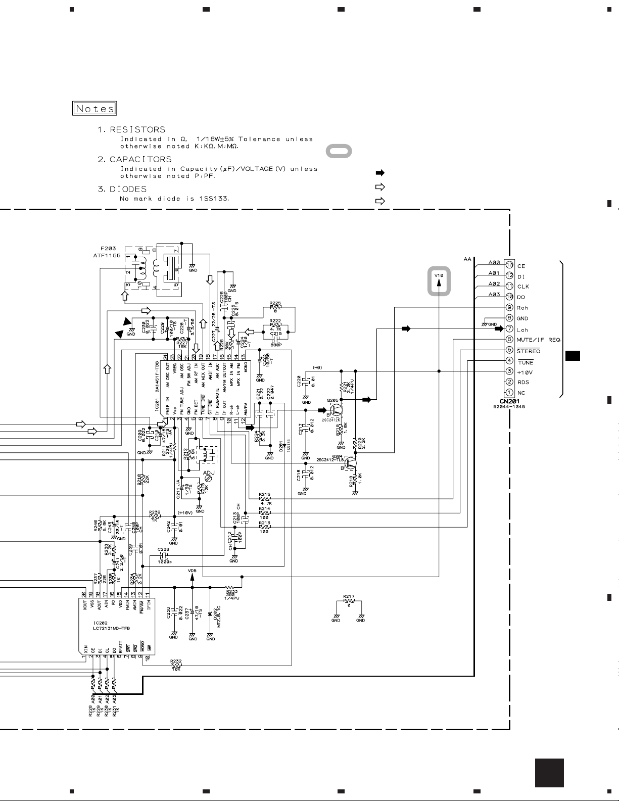
6.2 TUNER SECTION
AM Tuner Section
• There is no adjustment in the AM tuner.
FM Tuner Section
• Set the mode selector to FM BAND.
• Connect the wiring as shown in Fig. 1.
Step
No.
1
Adjustment
Title
T-METER
Adjustment
ANT. Input level and signal condition
Frequency
(MHz)
98 OFF 80
Modulation
Input Level
(dBµV)
Adjust
point
L201
Adjustment
Contents
Adjust L201 so that the DC voltage between Pin
21 and Pin 23 of IC201 (Test point Vtm) gets
within 0 ± 50mV.
MPX SG FM SG
FM75Ω antenna terminal
Fig.1 Adjustment Wiring Diagram
FM/AM TUNER UNIT
A
IC201
L201
pin 21
pin 23
PRODUCT
DC
Voltmeter
34
SIDE B
Fig.2 Adjustment Point
Page 35

7. GENERAL INFORMATION
7.1 DIAGNOSIS
7.1.1 DISASSEMBLY
XC-NS3V
STAND B
1
PUSH
STAND A
1
BOTTOM BASE
2
Stand B
1
1
2
Stand A
2
PULL
PCB Location
F
MOTOR UNIT
K
DISP UNIT
E
CD SW UNIT
J
LED UNIT
SELF-CHACK CD ASSY
B
KEY R UNIT
G
I
SENSOR UNIT
KEY L UNIT
H
3
REG B UNIT
DC
DB
A
MAIN UNIT
C
REG A UNIT
AUX UNIT
DA
FM/AM TUNER UNIT
35
Page 36

XC-NS3V
CD MECHA
Shaft Assy
Cam Base R
CAM BASE
×2
Shaft Assy
2
1
×2
1
1
×2
Cam Base L
2
4
4
4
5
3
CN1302CN1302
4
3
6
CD MECHA
7
6
5
CN1302CN1302
5
CN1201CN1201
MOTOR ASSY
2
2
3
5
7
×2
Unhook
6
2
1
CN1302CN1302
8
36
Page 37

Remove Shaft Assy and CD MECHA.
XC-NS3V
Installation position match of Shaft Assy
Shaft Assy
2
5
DISP UNIT,
DISP UNIT,
LED UNIT
LED UNIT
6
Reflector
1
CN13
CN14
2
4
3
CN16
3
1
The mark stand straight in line.
Be careful that Slide Cam doesn't move at fitting Shaft Assy.
2
Gear miss check point
2
8
6
8
9
6
8
6
7
9
8
White Gear turn full.
1
UPPER VIEW
2
Cam Base
Slide Cam
Both side
(L and R)
SIDE VIEW Both side (L and R)
3
OK
NG (Not fit this hook)
37
Page 38

XC-NS3V
7.1.2 SINGLE OPERATION METHOD
TEST MODE : ON
DC power supply
Connect each power
supply firmly stabilizing
as shown in the figure
below.
Service TEST mode. (STEST)
Refer to Fig. 1
TEST MODE
TEST
Short
MAIN UNIT
Refer to
6.1.1 How to
Start/Cancel
Service Test
Mode
DC power supply
TEST
MODE
An initial function becomes CD, then becomes CD TEST MODE. And becomes a blank display [ : ].
So that usual CD may operate, Return the function to the CD function again after making the function functions
other than CD. (The function can be changed by keeping pushing main body STOP key for two seconds. )
MAIN UNIT
C
SIDE B
DC power supply
GND
DC+9V
DC-9V
Short GNDU, GNDA
Fig. 1 DC power supply Point Location
Function and operation in service TEST mode.
Difference with the ordinary mode.
It is possible to operate even if there is no AC pulse.
It is possible to operate only in the CD tuner if a necessary DC power supply is supplied even if there is no part AMP.
The compulsion power off function by fan detection and the protecting function is released.
A wrong part was made easy to diagnose.
An initial function becomes CD TEST mode by CD and is usually different from the CD operation.
The function can be changed by keeping pushing main body STOP key for two seconds.
Other functions and the operations are the same as the ordinary mode.
TEST MODE : STOP
DC power supply
DC+5.6V
38
To come off the test mode, AC OFF.
The test mode is not completely cleared in POWER OFF key and AC OFF, please.
Page 39

XC-NS3V
7.2 PARTS
7.2.1 IC
• The information shown in the list is basic information and may not correspond exactly to that shown in the schematic diagrams.
List of IC
•
PDC073A, PD5601A, TA2150FN, TC9495F, MSM514260C-60TS, CL680T-D1, PDC065A
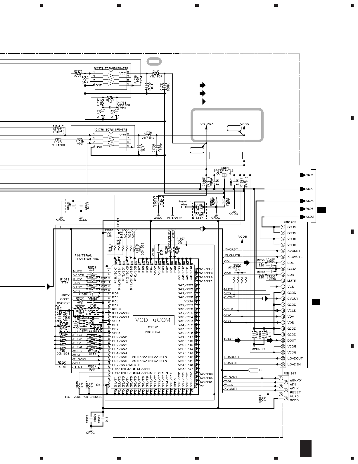
PDC073A (MAIN UNIT : IC5501)
• System Control IC
Pin Function
•
No. Pin Name I/O MOS Function Pin Function Active
1 BEEP O C Port BEEP Output 2 BUS0 I/O C Port CD LSI Communication Bus 3 BUCK O C Port CD LSI Communication Bus Clock 4 FLCE O C Port FL Driver CE
5 TXMUTE O C Port FM/AM Tuner module Mute
6 TXCLK O C Port FM/AM Tuner module Control Clock 7 TXDI O C Port FM/AM Tuner module Control Data
8 TXCE O C Port FM/AM Tuner module Control CE
9 XRDSON O C Port RDS Decoder Control (H : Stop) L
10 (DEBUG) O C Port Not used 11 XRESET I - RESET RESET L
12 (NC) - - Connect VDD1 for Not used 13 (NC) - - Open for Not used 14 GND - - GND GND 15 CF1 - - SERALOCK Seramic resonator Connected terminal 16 CF2 - - SERALOCK Seramic resonator Connected terminal 17 VDD - - VDD VDD 18 XFLRST O N Port FL Driver Hardware Reset L
19 KEY I N Anarog Input KEY Input 20 CD O/C I N Anarog Input CD DOOR SW Input 21 (NC) O N Port Not used 22 (NC) O N Port Not used 23 XCDRST O N Port CD LSI Hardware Reset L
24 PROTECT I N Anarog Input Measures of short test with Summing circuit 25 DSTN I N Anarog Input Destination Switch 26 ACPULSE I N INT0 Port AC Pulse Input 27 XCDCE O C INT1 Port CD LSI CE
28 RDSCLK I C INT2 Port Clock Input from RDS Decoder (Without RDS : Low Output) 29 RMC I C INT3 Port Remote Control Signal Input 30 (NC) O P VFD Controller Prohibition of use only for VFD 31 (NC) O P VFD Controller Prohibition of use only for VFD 32 (NC) O P VFD Controller Prohibition of use only for VFD 33 (NC) O P VFD Controller Prohibition of use only for VFD 34 (NC) O P VFD Controller Prohibition of use only for VFD 35 (NC) O P VFD Controller Prohibition of use only for VFD 36 (NC) O P VFD Controller Prohibition of use only for VFD 37 (NC) O P VFD Controller Prohibition of use only for VFD 38 (NC) O P VFD Controller Prohibition of use only for VFD 39 (NC) O P Port Not used 40 (NC) O P Port Not used 41 (NC) O P Port Not used 42 (NC) O P Port Not used 43 (NC) O P Port Not used 44 (NC) O P Port Not used 45 (NC) O P Port Not used 46 VDD - - VDD VDD 47 (NC) O P Port Not used 48 (NC) O P Port Not used 49 XCDDROFF O P Port CD Door Driver Control ON/OFF (0 : OFF, 1 : Drive ON) L
50 CDSLEEP O P Port CD LSI Function Stop (0 : OFF, LSI Stop : LSI Operation) H
39
Page 40

XC-NS3V
No. Pin Name I/O MOS Function Pin Function Active
51 GND - - 52 ZDET I P Port CD Zero Detection Input
53 CDINSIDE I P Port CD INSIDE SW Input
54 LOADIN O P Port CD Door Driver Control (Direction where door is closed
55 LOADOUT O P Port CD Door Driver Control (Direction where door is opened) H
56 XTMRLED O P Port Timer Standby Display LED Control L
57 XSTBYLED O P Port Standby Display LED Control L
58 DISCLED O P Port DISC LED Control, lights brightly *3 H
59 LEDDEMA O P Port DISC LED Control, lights a little darkly *3 H
60 LEDDEMB O P Port DISC LED Control, lights considerably darkly *3 H
61 XIRON O P Port Infrared RadiationControl for Sensor L
62 FLDIMA O P Port FL Dimmer Control A
63 FLDIMB O P Port FL Dimmer Control B
64 (NC) O P Port Not used
65 TXDO I P Port Data Input from FM/AM Tuner module 66 RDSDATA I P Port Data Input from RDS Decoder 67 XSTEREO I P Port STEREO Detection Input
68 XTUNED I P Port TUNED Detection Input L
69 ATT O P Port LINE Input ATT Control H
70 CDMUTE O P Port CD Output Mute H
71 4052B O P Port BU4052BCF Control A *1 72 VDD - - VDD VDD 73 4052A O P Port BU4052BCF Control B *1 74 (NC) O P Port Not used 75 XIRPOW O P Port Remote Control Microcomputer Power Supply Control L
76 TEST I P Port CD Core Checker Mode Detection Jumper L
77 UTEST I P Port Unit Test Mode Detection Jumper L
78 SERVICE I P Port Service Mode Detection Jumper L
79 (NC) O P Port Not used 80 WCLK I P Port For Flash Rewrite 81 (NC) O P Port Not used 82 (NC) O P Port Not used 83 SBDI I P Port System Bus Received Data 84 XEMR I P Port Signal of emergency generation from amplifier L
85 SBDO/REQ O C Port System Bus Sending Data / Request 86 SBCLK O C Port System Bus Clock 87 DREQ O C Port Display Data Communication Request 88 EXOE O C Port BU4094BCF Output E , Using combinedly with WD0 for Flash Rewrite *3 H
89 GND - - GND GND 90 VDD - - VDD VDD 91 EX/V DATA O C Port BU4094BCF / VOL-IC Control Data *3 92 EX/V CLK O C Port BU4094BCF / VOL-IC Control Clock *3 93 EXCE O C Port BU4094BCF CE , Using combinedly with WEN/D1 for Flash Rewrite *3 H
94 FLDATA O C Port FL Driver Control Data 95 FLCLK O C Port FL Driver Control Clock 96 DDATA I C Hard Serial Display Data Communication Received Data 97 DCLK I C Hard Serial Display Data Communication Clock 98 BUS3 I/O C Port CD LSI Communication Bus 99 BUS2 I/O C Port CD LSI Communication Bus -
100 BUS1 I/O C Port CD LSI Communication Bus -
)
H
40
Page 41

*1 : Change of function. The truth value table of BU4052BCF.
A B Switch turned on Function
L L X0, Y0 CD
H L X1, Y1 AUX
L H X2, Y2 PB
H H X3, Y3 TX
*2 : The truth value table of Expander IC (BU4094BCF / M-F10 COMPLEX ASSY IC5801).
Function Name Port Kind Active
OE C-MOS H
ACRY C-MOS H
SPRY C-MOS H
XMUTE C-MOS L
IND C-MOS H
HPPOW C-MOS (Not used)
WF1* C-MOS L
WF2* C-MOS L
*
Woofer Level WF1 WF2
HIGH H H
MID H L
LOW L H
*3 : The truth value table of PLAY LED brightness.
Brightness DISCLED LEDDIMA LEDDIMB
OFF L L L
LOW L L H
MID L H L
HIGH H L L
XC-NS3V
PD5601A (DISP UNIT : IC5652)
• 4 Bit Single Chip Microcomputer
Pin Assignment
•
VSS
E2
E1
XIN
XOUT
E0
G0
G2
G3
G4
Pin Function
•
NO. PIN NAME FUNCTION I/O PULL DOWN ACT at SLEEP NOTE
1 VSS GND – ––– – –––––
2 E2 Trigger input for buzzer I Software H I Pull down ON always
3 E1 Buzzer output O Software H I Pull down ON always
4 X IN 3.84MHz Oscillation Connection I ––– – –––––
5 X OUT 3.84MHz Oscillation Connection O ––– – –––––
6 E0 buzzer ON/OFF input I Software H Input interception Pull down OFF at SLEEP
7 G0 KEY input 1 I Software H I
8 G1 KEY input 2 I Software H I
9 G2 KEY input 3 I Software H I
10 G3 KEY input 4 I Software H I
11 D7 Signal switch output O Software H I
12 D6 Remote control output without carrier O External L H output
13 D5 KEY output O ––– H H output
14 D4 KEY output O ––– H H output
15 D3 KEY output O ––– H H output
16 D2 KEY output O ––– H H output
17 D1 KEY output O ––– H H output
18 D0 KEY output O ––– H H output
19 CARR Remote control output with carrier O ––– H L output
20 VDD 3V Power supply – ––– – –––––
1
2
3
4
5
6
7
8
9
10
20
VDD
19
CARR
18
D0
17
D1
16
D2
15
D3
14
D4
13
D5
12
D6
D7
11
41
Page 42

XC-NS3V
KEY No. KEY NAME TRANSMISSION CODE
1 4 / – A692
2 VOLUMEUP A60A
3 TUNER A649
4 ¢ / + A691
5 VOLUMEDN A60B
6 CD A644
7 STOP A690
8 TIMER A6CE
9 TAPEREC A114
10 MD REC A6A2+AF66
11 SET A674
12 DISPLAY A69D
13 TAPE A617
14 AUX A64C
15 POWER A61C
16 MENU A672
17 SOUND A6DA
18 MD A6A2+AF6D
19 CDR A6A0+AF35
20 CANCEL A673
21 1 A694
22 ¡ A693
23 CDR DOOR A6A0+AF6F
24 CD DOOR A6A0+AF6E
OPERATION EXPLANATION
•
D0 1 2 3 19
DI 4 5 6 20
D2 7 8 9 21
D3 10 11 12 22
D4 13 14 15 23
D5 16 17 18 24
G0 G1 G2 G3
It returns for the key input or the trigger input for the buzzer as SLEEP mode at time usually.
For "L" buzzer ON/OFF input.
Terminal CARR : The remote control code which corresponds to the pushed key is transmitted.
Carrier 40KHz, 1/3 Duty, Frame cycle 26ms.
Terminal E1 : If "H" pulse of 50-200ms is input two times between 0.5-1.5S in the terminal E2, the buzzer is output.
The buzzer is output if "H" pulse of 50-200ms is input two times between 0.5-1.5S in the terminal E2.
· Frequency of buzzer : 3KHz.
· How to sound the buzzer is as follows.
100ms sounding 100ms rest 100ms is sounded.
500ms rest, and 100ms repeated sounding, 100ms rest, and 100ms is sounded and it ends (Enter SLEEP).
*The buzzer is not output for 50ms or less and 200ms or more.
*The buzzer output is not done, except when the interval of the pulse of two times is 0.5-1.5S.
(Enter SLEEP when 1.5S is passed from the pulse of the first time.)
*This terminal is checked if there is no key input when returning from SLEEP.
(This terminal is not checked, except when returning for the key input.)
*When there is a key input when the width of the pulse and the interval are measured, the mode is made a key input
and the measurement of the pulse is discontinued.
Terminal D6 : "H" Fix.
Terminal D7 : "L" Fix.
For "H" buzzer ON/OFF input.
Terminal CARR : "L" Fix.
Terminal E1 : "L" Fix.
Terminal D6 : The remote control code which corresponds to the pushed key is transmitted.
There is no carrier.
Terminal D7 : Only when the remote control code is transmitted, "H" is output.
*It is made "H" before the remote control code is transmitted. After 10ms, it is made "L" after the key is turned off,
and the last remote control code is transmitted.
42
Page 43

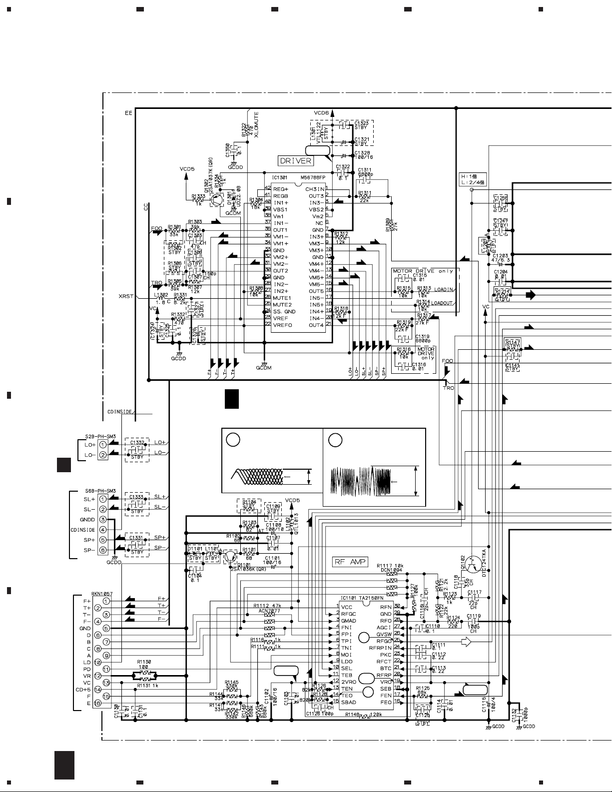
TA2150FN (SELF-CHUCK VCD ASSY : IC1101)
• RF AMP. IC
Block Diagram
•
XC-NS3V
43
Page 44

XC-NS3V
Pin Function (1/2)
•
44
Page 45

Pin Function (2/2
•
XC-NS3V
)
45
Page 46

XC-NS3V
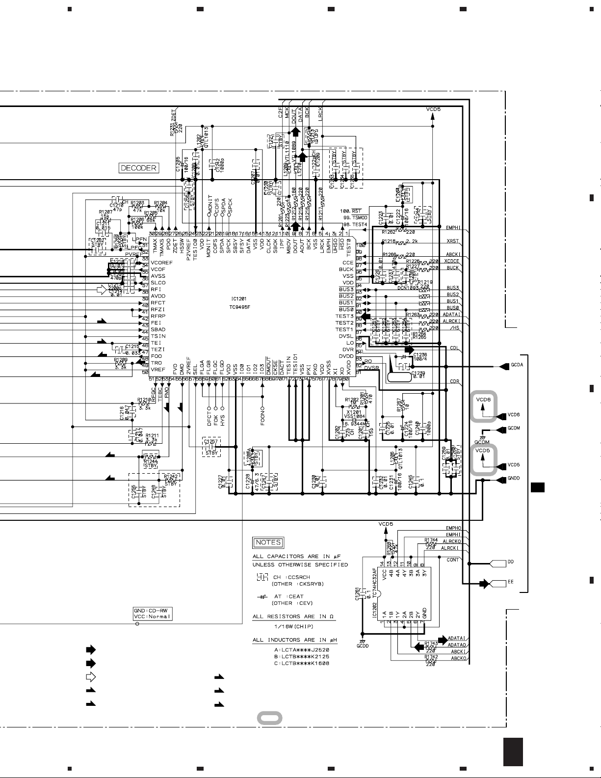
TC9495F (SELF-CHUCK VCD ASSY : IC1201)
• DECODER
46
Page 47

Pin Function (1/4)
•
XC-NS3V
47
Page 48

XC-NS3V
Pin Function (2/4)
•
48
Page 49

Pin Function (3/4)
•
XC-NS3V
49
Page 50

XC-NS3V
Pin Function (4/4)
•
50
Page 51

MSM514260C-60TS (SELF-CHUCK VCD ASSY : IC1756)
• 4M DRAM
Block Diagram
•
XC-NS3V
WE
Controller
RAS
LCAS
Timing
Generator
UCAS
Controller
A0 - A8
V
CC
9
9
Column
Address
Buffers
Internal
Address
Counter
Row
Address
Buffers
Refresh
Control Clock
Row
9
Decoders
Word
Drivers
Column Decoders
9
Sense Amplifiers
Memory
Cells
On Chip
Generator
V
BB
V
SS
CL680T-D1 (SELF-CHUCK VCD ASSY : IC1701)
• MPEG DECODER
I/O
I/O
OE
16
I/O
Selector
Output
Buffers
Input
Buffers
Input
Buffers
Output
Buffers
8
DQ1
-
DQ8
88
8
DQ9
-
DQ16
88
8
16
8
Block Diagram
•
Serial Bitstream
CD Subcode Data
HostData
Host
lnterface
CD
lnterace
lnternal Bus
RISC
CPU
DRAM/ROM
lnterface
DRAM and ROM
Decompression
Coprocessors
Video
Interface
Audio
Interface
Video Data
Audio Data
51
Page 52

XC-NS3V
PDC065A (SELF-CHUCK VCD ASSY : IC1501)
• VCD micro computer
Pin Function
•
No. Name I/O Description
1 HSEL I VCD IC (CL680T) communication (DATA
SELECT)
2 CDMUTE O CD MUTE control (H:MUTE)
3 XCDCE O CD BUS communication (TC9495F CHIP
ENABLE)
4 BUCK O CD BUS communication (TC9495F CLK
OUT)
5 /HS O CD IC (TC9495F) Nomal/High speed select
ACTIVE ("H" :NORMAL)
6 XRST I Reset output of TC9495F and CL680T
("L" : ACTIVE)
7 VCS I Communication with system microcomputer
(CHIP SELECT)
8 HRDY O VCD IC (CL680T) communication
(VCD communication permission)
9 CONT I "L" : ACTIVE for CD IC (TC9495F)
(INITAL CONTROL) H: RESET period
10 NC I 11 XVCRST O Reset input
12 (+5V) O Because it is unused, connects with +5V.
13 NC O 14 GND O GND
15 CF1 O Connects with a ceramic oscillator (10MHZ)
16 CF2 O Connects with a ceramic oscillator (10MHZ)
17 VDD O Connects with a +5V
18 BUS3 O
19 BUS2 O CD BUS communication (TC9495F DATA
20 BUS1 O INPUT OUTPUT)
21 BUS0 O
22 WCLK O The terminal (It is unused in the mask ROM)
(I) for the flash microcomputer writing
23 ED0 O The terminal (It is unused in the mask ROM)
(I/O) for the flash microcomputer writing
24 WEN/D1 O The terminal (It is unused in the mask ROM)
(I) for the flash microcomputer writing
25 VNR O VNR ON/OFF(H:N)
26 HINT O VCD IC (CL680T) communication interrupt
request
27 TEST1 O Checkers test mode input ("H" : MODE
START & CD PLAY
28 TEST2 O Checkers test mode end ("H" : CD STOP &
MODE END
29 NC O 30 connects with the terminal GND . (It is not
I (GND) - possible to use for VFD)
38
No. Name I/O Description
39
I GND - GND
45
46 VDD - GND
47
I (GND) - unused (GND connection)
50
51 VP - GND
52 -
I (GND) - unused (GND connection)
71 72 VDD - GND
73
I (GND) - unused (GND connection)
84
85 ZDET Zero detection ("H" : ZERO)
86 CD INSIDE I CD INSIDE SW ("L": INSIDE)
87
I (GND) - unused (GND connection)
89
90 VDD I +5V
91
I (GND) - unused (GND connection)
94
95 VCV O Communication with system microcomputer
(DATA INPUT/OUTPUT)
96 VCS I Communication with system microcomputer
(DATA INPUT)
97 VCLK I Communication with system microcomputer
(CLK)
98 NC O 99 HDIO I/O VCD IC (CL680T) DATA communication
(DATA INPUT/OUTPUT)
100 HCLK O VCD IC (CL680T) DATA communication
(CLK OUT)
52
Page 53

7.2.2 DISPLAY
AAV7077 (DISP UNIT : V5651)
• FL DISPLAY
62 1
1G13G 13G2G 3G 4G 5G 6G 7G 8G 9G 10G 11G 12G
SLEEP
SYNC
WAKE-UP
DIGITAL
L
R
RDSCD - RW
SKIP ON
ATT
FINALIZE
XC-NS3V
REC
RPT-1
D.VOL
PGM
TAPE
RDM
Anode Connection
P1 1-1
P2 2-1
P3 3-1
P4 4-1
P5 5-1
P6 1-2
P7 2-2
P8 3-2
P9 4-2
P10 5-2
P11 1-3
P12 2-3
P13 3-3
P14 4-3
P15 5-3
P16 1-4
P17 2-4
P18 3-4
P19 4-4
P20 5-4
P21 1-5
P22 2-5
P23 3-5
P24 4-5
P25 5-5
P26 1-6
P27 2-6
P28 3-6
P29 4-6
P30
P31
P32
P33
P34
P35
P36 − 2-0
P37 − 3-0
P38 − 5-0
13G 12G - 1G
RDS
SKIP
ON
REC
RPT
-1
ATT
D.VOL
PGM
RDM
FINALIZE
TAPE
−
−
−
−
−
−
−
WAKE-UP
L
R
DIGITAL
SYNC
SLEEP
W
- R
CD
5-6
1-7
2-7
3-7
4-7
5-7
1-1
1-2
1-3
1-4
1-5
1-6
1-7
2-0
2-1
2-2
2-3
2-4
2-5
2-6
2-7
3-0
3-1
3-2
3-3
3-4
3-5
3-6
3-7
4-1
4-2
4-3
4-4
4-5
4-6
4-7
5-0
5-1
5-2
5-3
5-4
5-5
5-6
5-7
(1G - 12G)
Pin Connection
Pin No.
Connection
Pin No.
Connection
F1, F2 : Filament 1G~13G : GridNP : No Pin NC : No Connection NX : No Extend Pin DL : Datum Line
12345678910111213141516171819202122232425262728293031
F1 F1 NP NP
32 33 34 35 36 37 38 39 40 41 42 43 44 45 46 47 48 49 50 51 52 53 54 55 56 57 58 59 60 61 62
P28 P29 P30 P31 P32 P33 P34 P35
P1 P2 P3 P4 P5 P6 P7 P8 P9 P10 P11 P12 P13 P14 P15 P16 P17 P18 P19 P20 P21 P22
P36 P37 P38 13G 12G 11G 10G 9G 8G 7G 6G 5G 4G 3G 2G 1G NX NX NX NP NP F2 F2
P23 P24 P25 P26 P27
53
Page 54

XC-NS3V
8. PANEL FACILITIES AND SPECIFICATIONS
8.1 PANEL FACILITIES
7
6
5
4
3
2
1
8
9
CD/VCD tuner
CD/VCD tuner
1 Top cover – Remove to access the antenna
terminals, auxiliary inputs, and video output.
2 STANDBY/ON – Press to switch the system on or
into standby.
3 VOL – – Use to reduce the volume.
4 VOL + – Use to increase the volume.
5 7 (STOP) – Press to stop the currently playing
CD/VCD.
6 6 – Press to start CD/VCD playback, or pause a
disc that’s already playing (press again to restart).
7 OPEN/CLOSE – Press to open/close the disc
compartment.
8 Disc compartment – The disc compartment
automatically opens when you move your hand
near.
9 Standby indicator – Lights when the system is in
standby and lights green when the system is in
timer-standby mode.
123 4
CD - RW
SLEEP
SYNC
DIGITAL
WAKE-UP
567 8
ATT
FINALIZE
9
10 11 12
D.VOL
REC
PGM
Display
1 Tuning indicator – Lights when the tuner is tuned
to a broadcast.
2 FM stereo indicator – Lights when you’re listen-
ing to an FM broadcast in stereo.
3 FM mono indicator – Lights when you’re listen-
ing to an FM broadcast in mono.
4 RPT[-1] – Indicates the repeat mode (RPT for
repeat disc; RPT-1 for repeat track).
5 SLEEP – Lights when the sleep timer has been
set.
6 Record timer – Lights when the record timer has
been set for the MD recorder.
7 Timer set indicator – Indicates that the wake-up
and/or the record timer have been set.
8 WAKE UP – Lights when the wake up timer has
been set.
9 SYNC – Lights during automatic sync recording of
CDs.
10 ATT – Lights when the auxiliary input signal is
being attenuated (reduced in level).
11 PGM – Lights when a playlist has been pro-
grammed.
12 RDM – Lights during random track playback.
RPT-1
RDM
54
Page 55

About the automatic door open sensor
The automatic opening of the disc compartment
works using an infrared sensor. It may not work
reliably if:
• the sensor is exposed to direct sunlight
• the room is lit using fluorescent lights
• the unit is on a dark-colored surface
• the unit is placed adjacent to a wall or other
surface
Approximate transmitter range
Remote control
STANDBY/ON OPEN/CLOSE
1 2 3 4
MD AUX
5 6
7 8
SOUND
0
DIRECT PLAY
CD
NEXT
XC-NS3V
VOLUME
+–
TUNER
DISP/CHARA
40
20
15cm
Door open
sensor
On its default setting, the door open sensor may
open the disc compartment even if a CD is
playing. You can change this so that it will only
work if the CD player is stopped, or you can
switch it off altogether.
9
TIMER
RETURN
CANCEL MENUSET/SELECT
SLOW STEP REPEAT PROGRAM
1
25 26
GHI
4
PQRS WXYZ MARK
7
PBC
10 11
+
1312 14
–
1615 17
PREVIOUS
1918 20
22 2321 24
ABC DEF
2
JKL MNO
5
TUV
8
TIME SEARCH
3
6
9
DIGEST
27
28
STOP
LAST MEM.
30 3129 32
TV CHANNEL
33 34
TV/VIDEOTV TV VOLUME
35 38
36 37
+–
7
+–
55
Page 56

XC-NS3V
1 STANDBY/ON – Press to switch the system on or
into standby.
2 OPEN/CLOSE – Press to open/close the disc
compartment of the CD/VCD player.
3 VOLUME – – Use to adjust the volume.
4 VOLUME + – Use to adjust the volume.
5 MD – Press to switch to MD. If the system is in
standby, the power is also switched on. Playback
will start if there’s an MD loaded.
6 AUX – Press to switch to a component connected
to the auxiliary inputs. If the system is in standby,
the power is also switched on.
7 CD – Press to switch to CD/VCD. If the system is
in standby, the power is also switched on. Playback will start if there’s a disc loaded.
8 TUNER – Press to switch to the tuner. If the
system is in standby, the power is also switched
on.
9 SOUND – Press to select bass, treble, balance or
sub-woofer level (use the + and – buttons to
adjust the level).
10 NEXT ¢ + – Use to change menu options;
adjust the sound; change the preset station
number when listening to the radio; or skip
forward tracks on a CD, VCD or MD.
11 DISP/CHARA – Press to change the displayed
information (this varies according to the current
function).
12 1 – Press to scan backwards on the CD, VCD
or MD currently playing.
13 38 – Press to play a CD, VCD or MD. During
playback press to pause; press again to restart
playback.
14 ¡ – Press to scan forwards on the CD, VCD or
MD currently playing.
15 TIMER – Press to access the timer menu for
setting the wake-up, sleep and record timers.
16 PREVIOUS 4 – – Use to change menu options;
adjust the sound; change the preset station
number when listening to the radio; or skip back
tracks on a CD, VCD or MD.
17 7 STOP – Press to stop the currently playing CD,
VCD or MD.
19 SET/SELECT – Press to make a setting when
using the menu system. When playing a VCD
featuring Playback Control (PBC), press to select
an option from the PBC menu.
20 MENU – Press to access the menu system.
21 SLOW – During VCD playback, press to start
slow-motion play. Press again to change the
speed.
22 STEP E – During VCD playback, press to pause
playback. Press again to advance frame-by-frame.
23 REPEAT – Press to select a repeat mode.
24 PROGRAM – Press to start programming a track
playlist.
25 Number/letter buttons – Use for selecting tracks
and for naming station presets, MD tracks and
discs.
26 CLEAR – Press to clear tracks from the program
and clear tracks that have been input with the >10
button.
27 >10 – Use to select track numbers over 10.
28 MARK / 10/0 – Use for symbols and puntuation
marks when naming MD tracks or discs. Use as
10 or 0 when selecting track numbers.
29 PBC – Press to switch VCD Playback Control on/
off.
30 TIME SEARCH – Use to jump to a specific point
on a VCD.
31 DIGEST – Use to display several still frames of a
VCD on-screen for easy navigation of the disc.
32 LAST MEM. – Press to restart a VCD from the
place that it was last stopped rather than the
beginning of the disc.
The following buttons can only be used after
you’ve set up the remote to control your TV .
33 TV CHANNEL – – Press to change channels.
34 TV CHANNEL + – Press to change channels.
35 TV – Press to switch the TV on/off.
36 TV/VIDEO – Press to switch the input of the TV.
37 TV VOLUME – – Use to adjust the TV volume.
38 TV VOLUME + – Use to adjust the TV volume.
18 RETURN / CANCEL – Press to escape from
within a menu without changing any setting. When
playing a VCD featuring Playback Control (PBC),
press to return to the PBC menu.
56
Page 57

8.2 SPECIFICATIONS
XC-NS3V
Stereo CD/VCD Tuner: XC-NS3V
FM Tuner Section
Frequency Range................................................... 87.5 – 108MHz
Antenna...............................................................75 Ω, unbalanced
AM Tuner Section
Frequency Range.......................................... 531 kHz – 1,602 kHz
(9 kHz step)
530 kHz – 1,700 kHz (10 kHz step)
Antenna.....................................................................Loop antenna
Compact Disc Player Section
Type ......................................... Compact disc digital audio system
Usable discs............................................................ Compact discs
Channels ........................................................................ 2 (stereo)
Frequency Response ................................................. 4 Hz–20 kHz
Signal-to-Noise Ratio ............................................... 110 dB (EIAJ)
Wow and Flutter ........................................... Limit of measurement
(0.001%) or less (EIAJ)
Dimensions ................................ 205.5 (W) x 268 (H) x 66 (D) mm
(without stands and door closed)
Weight ................................................................................... 1.8 kg
Accessories
Remote control unit ....................................................................... 1
Stand A ......................................................................................... 1
Stand B ......................................................................................... 1
Paper pattern ................................................................................ 1
System cable................................................................................. 1
AC power cord .............................................................................. 1
FM wire antenna .......................................................................... 1
AM loop antenna ........................................................................... 1
Video cord ..................................................................................... 1
Batteries ........................................................................................ 2
Operating Instructions ................................................................... 1
Note: Specifications and design subject to possible modification
without notice, due to improvements.
ACCESSORIES
STANDBY/ON OPEN/CLOSE
VOLUME
0
+–
MD AUX
DIRECT PLAY
CD
TUNER
NEXT
SOUND
DISP/CHARA
+
–
TIMER
STOP
7
PREVIOUS
RETURN
CANCEL MENUSET/SELECT
SLOW STEP REPEAT PROGRAM
ABC DEF
3
2
1
JKL MNO
GHI
6
5
4
TUV
PQRS WXYZ MARK
9
8
7
PBC
TIME SEARCH
DIGEST
LAST MEM.
TV CHANNEL
+–
TV/VIDEOTV TV VOLUME
+–
Remote control unit
(AXD7282)
AC power cord
(ZBDXJ : ADG1158)
(ZLXJ/NC : ADG1154)
AA/R6P Dry Cell Batteries × 2
(VEM-013)
Yellow (L=1.5m)
Video Cord × 1
(VDE1010)
Stand A
(AXG7096)
Ferrite Core
(ATX7007)
System cable (ADE7057)
AM loop antenna
(ATB7009)
FM wire antenna
(ADH7004)
Stand B
(AXG7097)
57
 Loading...