

Page 1
VSX-522-K
AV Receiver
VSX-522-K
THIS MANUAL IS APPLICABLE TO THE FOLLOWING MODEL(S) AND TYPE(S).
Model Type Power Requirement Remarks
VSX-522-K CUXESM AC 120 V
ORDER NO .
RRV4296
K-MZV FEB.
2012 Printed in Japan
Page 2
1
WARNING
This product may contain a chemical known to the State of California to cause cancer, or birth defects or other reproductive
harm.
Health & Safety Code Section 25249.6 - Proposition 65
This service manual is intended for qualified service technicians; it is not meant for the casual do-ityourselfer. Qualified technicians have the necessary test equipment and tools, and have been trained
to properly and safely repair complex products such as those covered by this manual.
Improperly performed repairs can adversely affect the safety and reliability of the product and may
void the warranty. If you are not qualified to perform the repair of this product properly and safely, you
should not risk trying to do so and refer the repair to a qualified service technician.
1. SAFETY PRECAUTIONS
The following check should be performed for the
continued protection of the customer and service
technician.
LEAKAGE CURRENT CHECK
Measure leakage current to a known earth ground
(water pipe, conduit, etc.) by connecting a leakage
current tester such as Simpson Model 229-2 or
equivalent between the earth ground and all exposed
metal parts of the appliance (input/output terminals,
screwheads, metal overlays, control shaft, etc.). Plug
the AC line cord of the appliance directly into a 120 V
AC 60 Hz outlet and turn the AC power switch on. Any
current measured must not exceed 0.5 mA.
ANY MEASUREMENTS NOT WITHIN THE LIMITS
OUTLINED ABOVE ARE INDICATIVE OF A POTENTIAL
SHOCK HAZARD AND MUST BE CORRECTED BEFORE
RETURNING THE APPLIANCE TO THE CUSTOMER.
2. PRODUCT SAFETY NOTICE
Many electrical and mechanical parts in the appliance
have special safety related characteristics. These are
often not evident from visual inspection nor the protection
afforded by them necessarily can be obtained by using
replacement components rated for voltage, wattage, etc.
Replacement parts which have these special safety
characteristics are identified in this Service Manual.
Electrical components having such features are
identified by marking with a > on the schematics and on
the parts list in this Service Manual.
The use of a substitute replacement component which
does not have the same safety characteristics as the
PIONEER recommended replacement one, shown in the
parts list in this Service Manual, may create shock, fire,
or other hazards.
Product Safety is continuously under review and new
instructions are issued from time to time. For the latest
information, always consult the current PIONEER Service
Manual. A subscription to, or additional copies of,
PIONEER Service Manual may be obtained at a nominal
charge from PIONEER.
Leakage
current
tester
Reading should
not be above
0.5 mA
Device
under
test
Test all
exposed metal
surfaces
Also test with
plug reversed
(Using AC adapter
plug as required)
Earth
ground
AC Leakage Test
(FOR USA MODEL ONLY)
2 3 4
SAFETY INFORMATION
A
B
C
D
E
F
2
1
2 3 4
VSX-522-K
Page 3

5
6 7 8
CONTENTS
SAFETY INFORMATION..........................................................................................................................................................2
1. SERVICE PRECAUTIONS....................................................................................................................................................4
1.1 NOTES ON SOLDERING...............................................................................................................................................4
1.2 NOTES ON REPLACING PARTS.......................................... ... ... ............................... ... .................................................4
1.3 SERVICE NOTICE........................................ .............................................................. ... .................................................4
2. SPECIFICATIONS.................................................................................................................................................................5
3. BASIC ITEMS FOR SERVICE..............................................................................................................................................6
3.1 CHECK POINTS AFTER SERVICING ............................. ..............................................................................................6
3.2 JIGS LIST...... .. .............................................................. ... ..............................................................................................6
3.3 PCB LOCATIONS.................................... .. .....................................................................................................................7
4. BLOCK DIAGRAM................................................................................................................................................................8
4.1 OVERALL WIRING DIAGRAM .............................................. ... ......................................................................................8
4.2 AUDIO BLOCK DIAGRAM............................................. ... ............................... .. ...........................................................10
4.3 D-MAIN BLOCK DIAGRAM................................................................................................... ... ....................................12
4.4 POWER SUPPLY BLOCK DIAGRAM............................................. ... .................................... ... ... ... ..............................14
4.5 VIDEO BLOCK DIAGRAM.................................. ... .............................. ... .................................. ....................................16
5. DIAGNOSIS........................................................................................................................................................................17
5.1 TROUBLESHOOTING.................... ... .............................................................. .. ...........................................................17
5.2 USB/iPod ERROR MESSAGE......................................................................................................................................29
5.3 DETECTION CIRCUIT ......................... ... ............................................................. ... .....................................................30
5.4 IC INFORMATION .............................................. ... .......................................................................................................32
6. SERVICE MODE.................................................................................................................................................................38
6.1 SERVICE MODE...... ... .. ............................... ... .............................................................. .. .............................................38
7. DISASSEMBLY ...................................................................................................................................................................42
8. EACH SETTING AND ADJUSTMENT................................................................................................................................50
8.1 ADJUSTMENT REQUIRED WHEN THE UNIT IS REPAIRED OR REPLACED.......................................... .. ... ...........50
8.2 UPDATING OF THE FIRMWARE .................................................................................................................................51
8.3 IDLE CURRENT ADJUSTMENT..................................................................................................................................57
9. EXPLODED VIEWS AND PARTS LIST...............................................................................................................................58
9.1 PACKING SECTION..................................................................................... ... .. ...........................................................58
9.2 EXTERIOR SECTION .................... ... ... ............................... .. .......................................................................................60
10. SCHEMATIC DIAGRAM.............................................................................. ... ... ................................................................64
UDIO ASSY
10.1 A
10.2 AMP5 ASSY (1/2).......................................................................................................................................................66
10.3 AMP5 ASSY (2/2).......................................................................................................................................................68
10.4 MAIN ASSY................................................................................................................................................................70
10.5 D-MAIN ASSY (1/4)....................................................................................................................................................72
10.6 D-MAIN ASSY (2/4)....................................................................................................................................................74
10.7 D-MAIN ASSY (3/4)....................................................................................................................................................76
10.8 D-MAIN ASSY (4/4)....................................................................................................................................................78
10.9 VIDEO, G-L, G-R, WG-B and WG-A ASSYS..............................................................................................................80
10.10 BRG-A, BRG-B and BRG-C ASSYS ........................................................................................................................82
10.11 FRONT, INSEL, HP, MIC, F-USB and WG ASSYS...................................................................................................84
10.12 STANDBY ASSY.......................................................................................................................................................86
11. PCB CONNECTION DIAGRAM............................................ ... .................................... ... ... ...............................................88
11.1 AUDIO ASSY..............................................................................................................................................................88
11.2 AMP5 ASSY ...............................................................................................................................................................90
A
11.3 M
IN ASSY................................................................................................................................................................92
11.4 D-MAIN ASSY ............................................................................................................................................................96
11.5 VIDEO ASSY............................................................................................................................................................100
11.6 G-L, G-R, WG-B and WG-A ASSYS.........................................................................................................................101
11.7 BRG-A, BRG-B and BRG-C ASSYS ........................................................................................................................102
11.8 FRONT, INSEL, HP, MIC, F-USB and WG ASSYS...................................................................................................106
11.9 STANDBY ASSY.......................................................................................................................................................110
12. PCB PARTS LIST................................... .............................................................. .. .........................................................111
..............................................................................................................................................................64
A
B
C
D
E
F
VSX-522-K
5
6 7 8
3
Page 4
1
• For environmental protection, lead-free solder is used on the printed circuit boards mounted in this unit.
Be sure to use lead-free solder and a soldering iron that can meet specifications for use with lead-free solders for repairs
accompanied by reworking of soldering.
• Compared with conventional eutectic solders, lead-free solders have higher melting points, by approximately 40 ºC.
Therefore, for lead-free soldering, the tip temperature of a soldering iron must be set to around 373 ºC in general, although
the temperature depends on the heat capacity of the PC board on which reworking is required and the weight of the tip of
the soldering iron.
Do NOT use a soldering iron whose tip temperature cannot be controlled.
Compared with eutectic solders, lead-free solders have higher bond strengths but slower wetting times and higher melting
temperatures (hard to melt/easy to harden).
The following lead-free solders are available as service parts:
• Parts numbers of lead-free solder:
GYP1006 1.0 in dia.
GYP1007 0.6 in dia.
GYP1008 0.3 in dia.
The part listed below is difficult to replace as a discrete component part.
When the part listed in the table is defective, replace whole Assy.
Assy Name
D-MAIN Assy
HDMI Receiver —————— IC with heat-padIC2000
Parts that is Difficult to Replace
Ref No. Function Part No. Remarks
D-MAIN 3.3 V Power Supply IC —————— IC with heat-padIC2007
D-MAIN 5 V Power Supply IC —————— IC with heat-padIC2008
DSP 1.2 V Power Supply IC —————— IC with heat-padIC2013
DSP 1.8 V Power Supply IC —————— IC with heat-padIC2015
DSP IC —————— IC with heat-padIC2016
USB 5 V SW IC —————— IC with heat-padIC2024
• Discharging
For more detail, please refer to "7. DISASSEMBLY - 1. Discharging".
• Notes on Ground Points Connection
For more detail, please refer to "7. DISASSEMBLY - 2. Notes on Ground Points Connection".
2 3 4
1. SERVICE PRECAUTIONS
1.1 NOTES ON SOLDERING
A
B
C
1.2 NOTES ON REPLACING PARTS
D
E
F
1.3 SERVICE NOTICE
4
1
2 3 4
VSX-522-K
Page 5

5
Amplifier section
Continuous average power output of 80 watts* per
channel, min., at 8 ohms, from 20 Hz to 20 000 Hz with no
more than 0.08 %** total harmonic distortion.
Front (stereo)............................................................... 80 W + 80 W
Power output (1 kHz, 6 Ω, 1 %)...........................140 W per channel
Guaranteed speaker impedance.................................... 6 Ω to 16 Ω
* Measured pursuant to the Federal Trade Commission’s Trade
Regulation rule on Power Output Claims for Amplifiers
** Measured by Audio Spectrum Analyzer
Audio Section
Input (Sensitivity/Impedance)
LINE.........................................................................200 mV/47 kΩ
Signal-to-Noise Ratio (IHF, short circuited, A network)
LINE.......................................................................................98 dB
Signal-to-Noise Ratio [EIA, at 1 W (1 kHz)]
LINE.......................................................................................79 dB
Video Section
Signal level
Composite................................................................1 Vp-p (75 Ω)
Tuner Section
Frequency Range (FM) .................................87.5 MHz to 108 MHz
Antenna Input (FM)................................................75 Ω unbalanced
Frequency Range (AM)...................................530 kHz to 1700 kHz
Antenna (AM) .............................................................Loop antenna
Digital In/Out Section
HDMI terminal ...........................................................Type A (19-pin)
HDMI output type............................................................5 V, 100 mA
USB (iPod) terminal..............................USB2.0 Full Speed (Type A)
Miscellaneous
Power Requirements...............................................AC 120 V, 60 Hz
Power Consumption................................................................415 W
In standby...........................................................0.4 W (ARC OFF)
Dimensions....................435 mm (W) x 168 mm (H) x 342.5 mm (D)
17 3/16 in. (W) x 6 5/8 in. (H) x 13 1/2 in. (D)
Weight (without package).....................................8.7 kg (19 lb 3 oz)
Note
• Specifications and the design are subject to possible
modifications without notice, due to improvements.
Accessories
Remote control (AXD7660)
(8300766000010-IL)
AM loop antenna
(E601019000010-IL)
Warranty card
Quick start guide (5707000006490-IL)
Safety Brochure
Operating instructions (CD-ROM)(6517000000500-IL)
FM wire antenna
(E605010140010-IL)
Dry cell batteries
(AAA size IEC R03) x2
Microphone (for Auto MCACC setup)
(APM7010)
2. SPECIFICATIONS
6 7 8
A
B
C
D
E
F
VSX-522-K
5
6 7 8
5
Page 6
1
Items to be checked after servicing
To keep the product quality after servicing, confirm recommended check points shown below.
See the table below for the items to be checked regarding video and audio.
No.
Item to be checked regarding video Item to be checked regarding audio
Procedures Check points
1 Confirm whether the customer complain has been solved.
If the customer complain occurs with the particular source, such
as Dolby Digital, DTS, AAC, DVD-A and HDMI, input it for the
operation check.
The customer complain must not be reappeared.
Video, Audio and operations must be normal.
2 Check the analog audio playback.
(Make the analog connections with a DVD player.)
Each channel audio and operations must be normal.
3 Check the digital audio playback.
(Make the digital connections with a DVD player.)
Each channel audio and operations must be normal.
4 Check surround playback.
(Select Surround mode and check the multichannel operations
via the DSP circuit.)
Each channel audio and operations must be normal.
5 Check the video outputs.
(Connect with a DVD player.)
Video and operations must be normal.
6 Check the tuner (AM and FM) operations. Audio and operations must be normal.
7 Check the sound from headphone output. Sound must be normal, without noise.
8 Check the appearance of the product.
Block noise Distortion
Horizontal noise Noise
Flicker Volume too low
Disturbed image (video jumpiness) Volume too high
Too dark Volume fluctuating
Too bright Sound interrupted
Mottled color
No scratches or dirt on its appearance after receiving it for
service.
Jigs List
Jig Name Part No. Remarks
RS-232C update jig (Jig + 10P FFC) GGF1642
(Marketing product)
(Marketing product)
MAIN microcomputer firmware update
(RS-232C ↔ Rear panel)
RS-232C cable (9-pin to 9-pin, straight cable)
9P extension jig cable GGD1739 Diagnosis (AMP5 Assy ↔ AUDIO Assy)
Diagnosis (D-MAIN Assy ↔ BRG-C Assy)Board to board extension jig cable GGD1798
Diagnosis (D-MAIN Assy ↔ BRG-C Assy)Board to board extension jig cable GGD1799
Diagnosis (D-MAIN Assy ↔ BRG-A Assy)Board to board extension jig cable GGD1756
Lubricants and Glues List
Name Part No. Remarks
Silicon grease GEM1057 Refer to "9.2 EXTERIOR SECTION".
Silicon adhesive
GYA1011
(KE40RTV-W)
Refer to "9.2 EXTERIOR SECTION".
HDMI (SUB) & CEC microcomputer firmware update
(USB ↔ Rear panel)
RS-232C update jig GGF1646
USB cable (USB A-Type ↔ USB B-Type)
2 3 4
3. BASIC ITEMS FOR SERVICE
3.1 CHECK POINTS AFTER SERVICING
A
B
C
D
3.2 JIGS LIST
E
F
6
1
2 3 4
VSX-522-K
Page 7

5
NSP 1..PCB TTL ASSY MAIN 7025HK1106010-IL
2..MAIN ASSY 7028071611060-IL
2..G-R ASSY 7028071614060-IL
2..G-L ASSY 7028071615060-IL
2..WG-A ASSY 7028071616060-IL
2..WG-B ASSY 7028071617060-IL
NSP 1..PCB TTL ASSY VIDEO 7025HK1106012-IL
2..VIDEO ASSY 7028071631010-IL
2..STBY ASSY 7028071632010-IL
2..BRG-A ASSY 7028071633010-IL
2..BRG-B ASSY 7028071634010-IL
2..BRG-C ASSY 7028071635010-IL
NSP 1..PCB TTL ASSY AUDIO 7025HK1106013-IL
2..AUDIO ASSY 7028071641060-IL
NSP 1..PCB TTL ASSY DMAIN 7025HK1106014-IL
2..D-MAIN ASSY 7028071651010-IL
NSP 1..PCB TTL ASSY AMP5 7025HK1106015-IL
2..AMP5 ASSY 7028070243010-IL
NSP 1.PCB TTL ASSY FRONT 7025HK1106011-IL
2..FRONT ASSY 7028071621060-IL
2..HP ASSY 7028071622060-IL
2..INSEL ASSY 7028071623060-IL
2..MIC ASSY 7028071624060-IL
2..F-USB ASSY 7028071625060-IL
2..WG ASSY 7028071627060-IL
Mark No. Description Part No. Mark No. Description Part No.
LIST OF ASSEMBLIES
NOTES: - Parts marked by “NSP” are generally unavailable because they are not in our Master Spare Parts List.
-
The > mark found on some component parts indicates the importance of the safety factor of the part.
Therefore, when replacing, be sure to use parts of identical designation.
D
D-MAIN ASSY
K
BRG-B ASSY
L
BRG-C ASSY
J
BRG-A ASSY
Q
F-USB ASSY
G
G-R ASSY
I
WG-A ASSY
P
MIC ASSY
R
WG ASSY
A
AUDIO ASSY
B
AMP5 ASSY
C
MAIN ASSY
H
WG-B ASSY
E
VIDEO ASSY
S
STBY ASSY
F
G-L ASSY
N
INSEL ASSY
O
HP ASSY
M
FRONT ASSY
3.3 PCB LOCATIONS
6 7 8
A
B
C
D
5
6 7 8
VSX-522-K
E
F
7
Page 8

1
FROM MAIN TRANS
CP1 CP2 CP3
1AC 1AC 1AC
2GND2AC 2AGND
3AC 3AC 3AC
CP403 CN3
+HIGHB 1 1 +HIGHB
+HIGHB 2 2 +HIGHB
+HIGHB 3 3 +HIGHB
-HIGHB 4 4-HIGHB
-HIGHB 5 5-HIGHB
-HIGHB 6 6-HIGHB
HIGHGND7 7HIGHGND
HIGHGND 88HIGHGND
HIGHGND9 9HIGHGND
PREGND10 10PREGND
CP402 CN1
FL 1 1 FL
FR 2 2 FR
C3 3C
SL 4 4 SL
SR 5 5 SR
1FL 6AGND
1 +9.1V
2AGND7SR
CN404
2GNDA
1HP_DET
3SL 8 AGND
DC_DET4 1
3 -9.1V
2HP_RO
4AGND9FR
DC_DET3 2
4MIC
3GNDA
5C 10AGND
ASO_DET 3
5MIC_DET
4HP_LO
RADI_THERMAL4
CN901 CN721 CP401 TR_THERMAL5
CN5
DGND1 1
CP901 CP721
DGND1
2
1M
IC DET 1HP LO
+12V
3
2MIC 2GNDHP
+12V
4
3 NC3HP RO
4 -9.1V 4HP DET
5GNDA
CP204
6 +9.1V
HP_DET 1
MIC_DET 2
VOL_DATA 3
VOL_CLK 4
SW_SUM 5
HP_RLY 6
A MUTE 7
SB MUTE 8
NC9
CN400
CP402 CN402
HP LO 1 1 HP_LO
1FL 6GNDA
GNDA 2 2 GNDA
2GNDA 7 SR
HP RO 3 3 HP_RO
3SL 8 GNDA
Z2 MUTE 4 4 Z2_MUTE
4GNDA 9 FR
SB MUTE 5 5 SB_MUTE
5 C 10 GNDA
AMUTE 6 6 A_MUTE
HPRLY 7 7 HP_RLY
SW SUM 88SW_SUM
Z2VOL DATA 9 9 Z2VOL_DATA
Z2VOL CLK10 10 Z2VOL_CLK
VOL DATA 11 11VOL_DATA
VOL CLK 12 12VOL_CLK
+12V 13 13+12V
GNDA 14 14GNDA
CN401
CP17
MIC 15 15 MIC
MUTE_B+ 1 1 MUTE_B+
GND
A
16 16 GNDA
+12V 2 2A+12V
-12V 17 17-12V
+12V 3 3A+12V
GNDA 4 4 AGND
GNDA 5 5 AGND
-12V 66A-12V
-12V 77A-12V
CP13
GNDA 88AGND
U/DGND1
1SBLIN 11SRIN
BT_R 9 9 BT_R
TUNER_INT2
2GNDA 12GNDA
GNDA 10 10 AGND
TUNER_SDIO3
3SBRIN 13 FLIN
BT_L11 11BT_L
TUNER_SCLK4
4GNDA 14GNDA
GNDA 12 12 AGND
TUNER_SEN5
5SWIN 15 FRIN
TUNER_R13 13 TU_R
TUNER_
RST 6
6GNDA 16GNDA
GNDA 14 14 AGND
2533_CTL 7
7CIN 17 AIN_L
TUNER_L15 15 TU_L
8 GNDA 18GNDA
9SLIN 19AIN_R
10 GNDA
CN403
CP403
1 SBL_OUT 11SR_OUT
CP16
2GNDA 12 GNDA
OSD_RST 1
3 SBR_OUT 13 FL_OUT
OSD_CE 2
4GNDA 14 GNDA
OSD_CLK 3
5SW_OUT 15FR_OUT
OSD_DATA 4
6GNDA 16 GNDA
CTL_A 5
7C_OUT 17AIN_L
CTL_B 6
8 GNDA 18GNDA
U/DGND7
9SL_OUT 19AIN_R
+5V8
10 GNDA
VIDEO_MUTE9
CP15
U/DGND1
CN9
CP9
MUT
E_B+ 2
OSD_RST 1 1 OSD_RST
U/DGND3
OSD_CE 2 2 OSD_CE
FBRL 4
OSD_CLK 3 3 OSD_CLK
SBRL 5
OSD_DATA 4 4 OSD_DATA
SURL 6
CTL_A 5 5 CTL_A
CRL 7
CTL_B 6 6 CTL_B
FRL 8
U/DGND 7 7 U/DGND
DC_PRO 9
+5V8 8+5V
-VF(-30V)10
VIDEO_MUTE9 9 VIDEO_MUTE
U/DGND11
-
When ordering service parts, be sure to refer to "EXPLODED VIEWS and PARTS LIST" or "PCB PARTS LIST".
-
The > mark found on some component parts indicates the importance of the safety factor of the part.
Therefore, when replacing, be sure to use parts of identical designation.
B
B
1/2-B2/2
A
AUDIO ASSY
(7028071641060-IL)
J
BRG-A ASSY
(7028071633010-IL)
K
BRG-B ASSY
(7028071634010-IL)
E
VIDEO ASSY
(7028071631010-IL)
O
HP ASSY
(7028071622060-IL)
P
MIC ASSY
(7028071624060-IL)
H
WG-B ASSY
(7028071617060-IL)
C
MAIN ASSY
(7028071611060-IL)
AMP5 ASSY
(7028070243010-IL)
I
WG-A ASSY
(7028071616060-IL)
R
WG ASSY
(7028071627060-IL)
F
G-L ASSY
(7028071615060-IL)
G
G-R ASSY
(7028071614060-IL)
2 3 4
4. BLOCK DIAGRAM
4.1 OVERALL WIRING DIAGRAM
A
B
C
D
E
F
8
1
2 3 4
VSX-522-K
Page 9

5
CN702
CP702
STBY_KEY 4 1 STBY_KEY
INPUT_UP 3 2 INPUT_UP
GNDU 2 3 GNDU
INPUT_DOWN 14INPUT_DOWN
1-30V 13 FLR_DATA
2-30V 14 FLT_CLK
3CPU_ST_VCC 15 FLT_CE
1HDMI+12V
4CPU_ST_VCC 16 INPUT_UP
2 STBY RLY
5GNDU 17 KEY2
3PDN
6GNDU 18KEY3
4CPU ST VCC
7 CPU_+3.3V 19 KEY1 (STBY_KEY)
5 CPU_+3.3V
8 CPU_+3.3V 20 INPUT_DN
6GNDU
9ST_H+5V 21VOL_UP
1GNDUSB
7FL2
10 POWERDOWN 22VOL_DN
2D+
8 FLCT
11 RMC 23THRU_LED
3D-
9FL1
12 STBY_RLY
4GNDUSB
AC 1 AC
5U
S
B+5V
CN701 CN704AA
CN2006
CP301
LIVE1
CP701
AC CORD
1FLAC
NEUTRAL 2
2FLCT
3FLAC
CP303
4CPU G ND
CN704B
CP2006
1
5CPU+3.3V
1THRU LED 13RMC
1UCHGND
VOL SEL 2
6STBY VCC
2 VOL DN 14 POWER DN
2D+
3
7PDN
3 VOL UP 15 H+5V
3D-
8 STBY RLY
4IN DN 16 CPU+3.3V
4USBGND
CP302
9CPU_ST_VCC
5KEY1 17CPU+3.3V
5USB+5V
1
6KEY3 18 ST VCC
TRANS
7KEY2 19ST VCC
2
8 IN UP 20 GNDU
9 F
LT CE 21 GNDU
CP304
10 FLT CLK 22 FL-30V
FLAC 1
11 FLT DATA 23 FL-30V
TRANSFLCT 2
12 STBY RLY
FLAC 3
CP2005
1DC D ET4
2DC D ET3
3ASO_DET
4RADI_DET
5 TRTHER_DET
CN5
CP2004
DGND1 1 1D+12V
DGND1 2 2D+12V
+12V
3 3DGND
+12V
4 4DGND
CN204
1HP DET
2MIC DET
3 VOL DATA
4 VOL CLK
5SW SUM
6 HP RLY
7A MUT E
8 SB MUTE
9 NC
CP2001
CN2001
HP DET 1 1 HP DET
MIC DET 2 2 MIC DET
VOL DATA 3 3 VOL DATA
VOL CLK 4 4 VOL CLK
SB MUTE 5 5 SB MUTE
A MUTE 6 6 A MUTE
SW SUM 7 7 SW SUM
HP RLY 88HP RLY
CP13
CN13
GNDU 9 9 GNDU
U/DGND1 1GNDU
FL-30V 10 10 FL-30V
TUNER_INT2 2TUNER INT
DC DET11 11 DC DET
TUNER_SDIO3 3 TUNER SDIO
F RLY 12 12 F RLY
TUNER_SCLK4 4 TUNER SCLK
C RLY 13 13 C RLY
TUNER_SEN55TUNER SEN
S RLY 14 14S RLY
TUNER_RST6 6 TUNER RST
M
U
TE B+15 15 MUTE B+
2533_CTL 7 7 NC
GNDU16 16 GNDU
TUNER SCLK17 17TUNER SCLK
TUNER SDIO 1 8 18 TUNER SDIO
TUNER SEN19 19 TUNER SEN
TUNER RST20 20 TUNER RST
TUNER INT21 21 TUNER INT
V CTL B 22 22 BH76330 B
V CTL A 23 23 BH76330 A
OSD DATA24 24 OSD DATA
OSD CLK25 25 OSD CLK
OSD CE 26 26 OSD CE
OSD RST27 27 OSD RST
CP16
CN16
OSD_RST 1 1 OSD RST
OSD_CE 2 2 OSD CE
OSD_CLK 3 3 OSD CLK
OSD_DATA 4 4 OSD DATA
CTL_A 5 5 V CTL A
CP2002
CN2002
CTL_B 6 6 V CTL B
V+5V 11V+5V
U/DGND7 7GNDU
CPU+3.3V 2 2 CPU+3.3V
+5V8 8V+5V(A+5V)
VIDEO MUTE 3 3 VIDEO MUTE
VIDEO_MUTE9 9 VID
EO MUTE
SC
LK JTAG 4 4 SCLK JTAG
BUSY JTAG 5 5 BUSY JTAG
CE 6 6 CE
EPM UP 7 7 EPM UP
CP15
CN11
CNVSS UP 88CNVSS UP
U/DGND1 1GNDU
232 TX/U RX 9 9 232TX/U RX
1AINR11SL
MUTE_B+ 2 2 MUTE B +
232 RX/U TX 10 10 232RX/U T X
2AGND12AGND
U/DGND3 3GNDU
RESET11 11 RESET
3AINL13C
FBRL 4 4 NC
CEC RXD12 12 CEC RXD
4AGND14AGND
SBRL 5 5 NC
CEC TXD13 13 CEC TXD
5FR 15SW
SURL 6 6 S RLY
CEC OPO14 14 CEC OPO
6AGND16AGND
CRL 7 7 C RLY
SUB RXD15 15 SUB RXD
7FL 17SBR
FRL 88F RLY
SUB TXD 16 16 SUB TXD
8 AGND18 AGND
DC_PRO 9 9 DC DET
GNDD 17 17 GNDD
9SR 19SBL
-VF(-30V) 10 10 FL-30V
SUB OPO 18 18 SUB OPO
10 AGND
U/DGND1
1 1
1GNDU
H+5V 19 19 H+5V
CN2003
CP2003
1AIN R 11 SL OUT
2GNDA 12 GNDA
3AIN L13C OUT
4GNDA 14 GNDA
5FR OU T 15SW OUT
6GNDA 16 GNDA
7 FL OUT 17 SBR OUT
8 GNDA 18GNDA
9 SR OUT 19 SBL OUT
10 GNDA
STBYB'D
L
BRG-C ASSY
(7028071635010-IL)
S
STBY ASSY
(7028071632010-IL)
M
FRONT ASSY
(7028071621060-IL)
N
INSEL ASSY
(7028071623060-IL)
Q
F-USB ASSY
(7028071625060-IL)
611060-IL)
D
D
1/4-D4/4
D-MAIN ASSY
(7028071651010-IL)
6 7 8
A
5
6 7 8
VSX-522-K
B
C
D
E
F
9
Page 10

1
A
AUDIO ASSY
M
FRONT ASSY
P
MIC ASSY
4.2 AUDIO BLOCK DIAGRAM
A
B
2 3 4
C
D
E
F
10
1
2 3 4
VSX-522-K
Page 11

5
O
HP ASSY
C
MAIN ASSY
Q
F-USB ASSY
B
AMP5 ASSY
6 7 8
A
B
C
D
E
F
VSX-522-K
5
6 7 8
11
Page 12

1
Q2035
4.3 D-MAIN BLOCK DIAGRAM
A
B
2 3 4
C
D
E
F
12
1
2 3 4
VSX-522-K
Page 13

5
Q2035
1 6
2
3
5
4
Q2034
FDC608PZ
D
D-MAIN ASSY
6 7 8
A
B
C
D
E
F
VSX-522-K
5
6 7 8
13
Page 14
1
S4(FLT)
S2(+12V,-12V)
S1(AMP B+/B-)
AC CORD
(922L/822:USB)
S3(522:DSP, HDMI)
MAIN TRANS
SUB TRANS
S
STBY ASSY
2 3 4
4.4 POWER SUPPLY BLOCK DIAGRAM
A
B
C
D
E
F
14
1
2 3 4
VSX-522-K
Page 15
5
Q2031
Q2029
Q2027
Q2035
1 6
2
3
5
4
Q2030
FDC608PZ
1234
5 6 7 8
IC2025
TPS2557
GND
IN
IN
EN
OUT
OUT
LIM
FAULT
1 6
2
3
5
4
Q2026
FDC608PZ
1 6
2
3
5
4
Q2028
FDC608PZ
1 6
2
3
5
4
Q2032
FDC608PZ
Q2033
1 6
2
3
5
4
Q2034
FDC608PZ
6 7 8
A
B
C
D
E
F
VSX-522-K
5
6 7 8
15
Page 16
1
BD
75
75
SAT
E
VIDEO ASSY
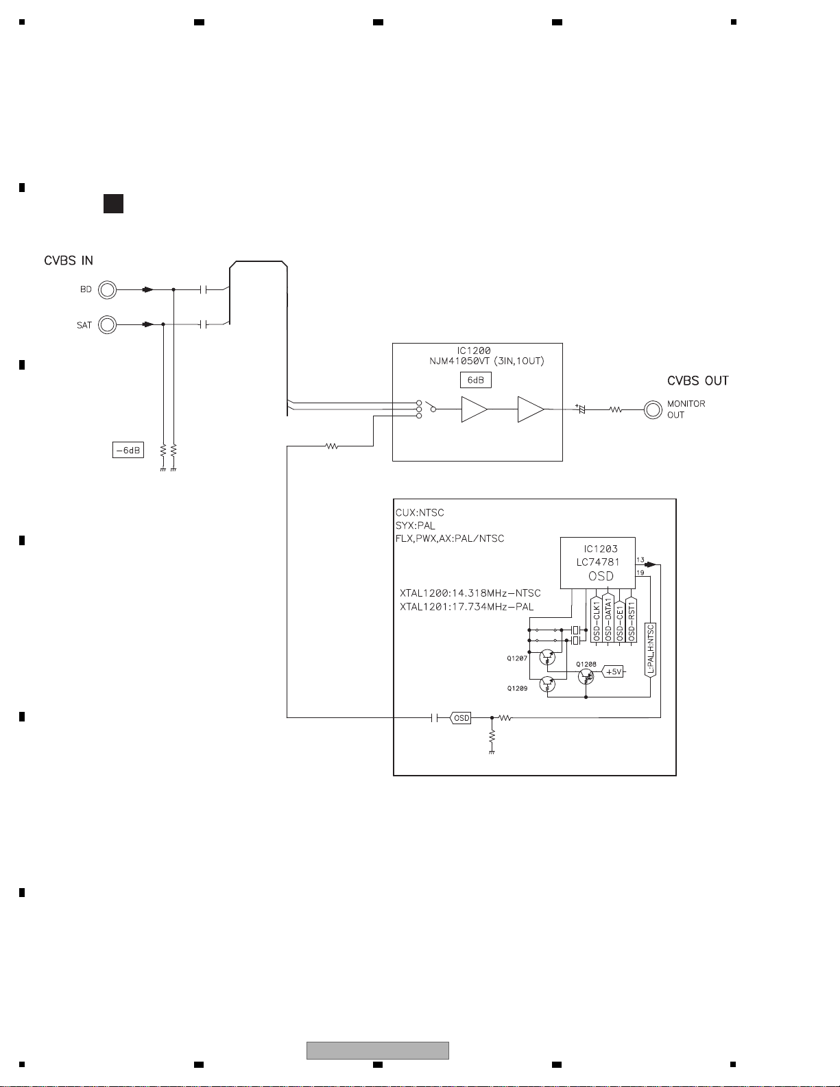
4.5 VIDEO BLOCK DIAGRAM
A
B
2 3 4
C
D
E
F
16
1
2 3 4
VSX-522-K
Page 17

5
Step 0: Preliminary confirmation
CN2002, CN2001, CN2003, CP2004
To Step 1
Are the connectors
securely inserted?
Step 1: Fixed board
Confirm the following items before checking
To Step 2
Tighten screws securely.
Do screws of back chassis
securely tighten?
Yes
Yes
B to B connector, wire
Yes
No
Insert the connectors
completely.
No
Step 2: Power supply
IC2007 (pin 2)
L2007
Is the voltage 12 V?
Check the IC2007 and its
peripheral circuits.
Is the voltage 3.3 V output?
Is pin 7 (en) of IC2007 high?
Is the voltage of 1.2 V output?
IC2013 (pin 2)
Check the IC2016 DSP power pin (cvdd and
dvdd): cvdd: 1.2 V, dvdd: 3.3 V.
Yes
Yes
+3.3V line of D-MAIN Assy is OK.
OK
Yes
No OK
Check the peripheral circuits or the
MAIN microcomputer (IC2023).
Check the IC2016 DSP
power pin (cvdd and dvdd)
and its peripheral circuits
or must be replaced
IC2016, IC2013.
No
No
No
Replace IC2007.
OK
Replace IC2007 or
check the MAIN Assy.
12 V input
(to chassis)
Is the voltage of 1.8 V output?
IC2005 (pin 5)
Check the IC2000 HDMI power pin
(acvdd33 and advdd18): 3.3 V, 1.8 V.
+3.3V line of D-MAIN Assy is OK.
OK
Yes
Check the IC2000 HDMI
power pin (avdd33 and
advdd18) and its peripheral
circuits or must be replaced
IC2000, IC2005.
No
(to chassis)
[1] DSP TROUBLESHOOTING
TROUBLESHOOTING FOR ALL DESTINATION
5. DIAGNOSIS
5.1 TROUBLESHOOTING
6 7 8
A
B
C
D
E
F
VSX-522-K
5
6 7 8
17
Page 18

1
Yes
Step 3: Power supply
CP2004 (pins 1, 2)
IC2008 (pin 2)
L2008
Is the voltage of 12 V?
Check the wire between
D-MAIN and MAIN Assemblies.
Check the IC2008 and
its peripheral circuits.
Is the voltage of 1.2 V input?
Yes
No
No
Is the voltage of 5 V output?
Yes
No
NG
OK
Check the MAIN Assy.
Replace IC2008.
12 V input
12 V input
Is pin 7 (en) of IC2008 high?
Yes
Check the IC2011 power pin (dvdd and
avdd): dvdd: 5 V, avdd: 5 V.
+5V line of D-MAIN Assy is OK.
OK
Check the peripheral circuits or the
MAIN microcomputer (IC2023).
No
Replace IC2008.
OK
Yes
Step 4: X'tal
IC2011 (pins 6, 7)
IC2014 (pin 2)
Is there a 24.576 MHz
output?
Check the IC2011 and its peripheral
circuits or replace XTAL2002.
No
Yes
Is there a 24.576 MHz
input?
Check the IC2014 and its peripheral
circuits or replace IC2011.
No
To Step 5
A
2 3 4
B
C
D
E
F
18
1
2 3 4
VSX-522-K
Page 19

5
Yes
Step 5: DIR
IC2009 (pin 3)
IC2011 (pin 61)
IC2011 (pin 67)
Can observe the
digital signal?
Check the path to INPUT pin of
JACK2006 or replace JACK2006.
Check that the S/PDIF signal is input.
Check that changes by pulling out and inserting the digital input lines.
No
Yes
Can observe the
digital signal?
Check the pass to IC2009 pin 4
or replace IC2009.
Can observe the
digital signal?
Yes
No
Check the path to pins 8 to 11 of
IC2009 or replace IC2009.
No
coax
opt
(0 V ↔ 3.3 V)
(0 V ↔ 3.3 V)
(0 V ↔ 3.3 V)
IC2011 (pin 69)
Can observe the
digital signal?
Yes
Check the path to pin 5 of IC2009 or
replace IC2009.
No
HDMI
(0 V ↔ 3.3 V)
IC2011 (pin 59)
Can observe the
digital signal?
Yes
Check the path to pins 1, 12 of
IC2009 or replace IC2009.
No
ARC
(0 V ↔ 3.3 V)
SPDIF INPUT line is OK.
Yes
Yes
No
Check the IC2011 and its peripheral
circuits of IC2011.
No
Check the IC2014 and its peripheral
circuits of IC2014.
OK
Check the pin 58 of IC2023,
is the voltage 3.3 V?
No
No
Replace IC2011, IC2014.
Check the IC2023 and
its peripheral circuits or
replace IC2023.
Check the peripheral circuits
between IC2011 and IC2023.
OK
IC2011 (pin 10)
IC2011 (pin 16)
Yes
Is there a master clock
24.576 MHz output?
Is the voltage of PDN IC2011
pin 31 3.3V?
Is there a LR clock
output?
DIR_MCK (master clock)
DIR_LRCK (LR CLOCK)
(0 V ↔ 3.3 V)
(0 V ↔ 3.3 V)
Check that the data and clock signals are output.
A
6 7 8
A
B
C
D
E
F
VSX-522-K
5
6 7 8
19
Page 20

1
Replace IC2011, IC2014.
Replace IC2014.
OK
IC2011 (pin 14)
Yes
Yes
Yes
IC2011 (pin 15)
IC2014 (pin 4)
DIR output is OK.
Is there a DATA output?
Is there a master clock
24.576 MHz output?
Yes
Is the voltage of IC2014
pin 1 0 V?
Is there a bit clock output?
DIR_SDTO (DATA)
DIR_BCK (bit clock)
DAI_MCK (MASTER CLOCK)
*IC2014 pin 1
0 V: DIR
3.3 V: HDMI
SWITCH
(0 V ↔ 3.3 V)
(0 V ↔ 3.3 V)
(0 V ↔ 3.3 V)
Check the IC2011 and its peripheral
circuits of IC2011.
No
Check the path between IC2014 pin 1
and IC2023 pin 70.
No
Replace IC2011.
OK
Check the IC2011 and its peripheral
circuits of IC2011.
Check the IC2014 and its peripheral
circuits of IC2014.
No
No
OK
A
Yes
Step 6: ADC
CN2003 (pins 1, 3)
IC2011 (pin 17)
IC2011 (pin 18)
Is there a analog audio
signal?
Is there a analog
audio signal of BRG-A Assy
CP403 pins 17, 19?
Check that the ANALOG input to DSP mode.
Yes
No
No
Replace CP2003 wafer of BRG-A Assy,
or reconnect BRG-A Assy.
Is there a data
output?
Yes
ANALOG AUDIO input
ADC_SDTO (ADC AUDIO OUT)
DSP_BCK
(0 V ↔ 3.3 V)
Check the AUDIO Assy.
No
Is there a bit clock
3.072 MHz input?
Yes
(0 V ↔ 3.3 V)
No
IC2011 (pin 19)
DSP_LRCK
Is there a LR clock
48 kHz input?
Yes
(0 V ↔ 3.3 V)
No
To Step 7
Check the path between IC2016 and data & address lines.
SDRAM (IC2018), FLASH ROM (IC2019), replace IC2016.
A
2 3 4
B
C
D
E
F
20
1
2 3 4
VSX-522-K
Page 21

5
Yes
Step 7: DSP mode audio output
IC2011(pin 18)
IC2011 (pin 19)
Is there a bit clock input?
Digital output of each CH when inputting the digital signal with audio.
Is there a LR clock
output?
Is there a data input?
Is there a data input?
Is there a data input?
Is there a data input?
Yes
IC2011 (pin 28)
IC2011 (pin 27)
Yes
IC2011 (pin 26)
Yes
IC2011 (pin 25)
Yes
Yes
DSP_BCK (BIT CLOCK)
DSP_LRCK (LR CLOCK)
front L/R data
surround L/R data
CENTER/LFE data
surround back L/R data
or front hight L/R data
(0 V ↔ 3.3 V)
(0 V ↔ 3.3 V)
(0 V ↔ 3.3 V)
(0 V ↔ 3.3 V)
(0 V ↔ 3.3 V)
(0 V ↔ 3.3 V)
To Step 8
No
No
No
No
No
No
Check the path between IC2016 and data & address lines.
SDRAM (IC2018), FLASH ROM (IC2019), replace IC2016.
6 7 8
A
B
C
D
E
F
VSX-522-K
5
6 7 8
21
Page 22

1
Yes
Step 8: CODEC output (ANALOG AUDIO OUT)
IC2011 (pin 49)
IC2011 (pin 47)
Is there a audio signal
output?
Analog output of each CH when inputting the digital signal with audio.
Analog output of each CH when inputting
the digital signal (-∞ dB(no signal)).
Yes
Is there a audio signal
output?
front R out
front L out
IC2011 (pin 45)
Yes
Is there a audio signal
output?
surround R out
IC2011 (pin 43)
Yes
Is there a audio signal
output?
surround L out
IC2011 (pin 43)
surround L out
IC2011 (pin 41)
Yes
Is there a audio signal
output?
center out
Yes
IC2011 (pin 41)
center out
IC2011 (pin 39)
Yes
Is there a audio signal
output?
LFE out
Yes
Yes
IC2011 (pin 39)
LFE out
IC2011 (pin 49)
Yes
Is the output 2.5 V fixing?
front R out
IC2011 (pin 47)
Yes
Is the output 2.5 V fixing?
front L out
IC2011 (pin 45)
Yes
Is the output 2.5 V fixing?
Is the output 2.5 V fixing?
Is the output 2.5 V fixing?
Is the output 2.5 V fixing?
surround R out
End
No
No
No
No
No
No
No
No
No
No
No
No
Replace IC2011.
A
2 3 4
B
C
D
E
F
22
VSX-522-K
1
2 3 4
Page 23

5
Cause for noncomplection of HDMI authentication between the source equipment and this unit.
(the HDMI indicator is unlit or flasher)
Causes for no display or sound from the monitor
[2] HDMI TROUBLESHOOTING
Replace the HDMI cable.
NG
OK
Replace the HDMI cable.
Connect the source equipment
(player) to the Sink equipment
(monitor) directly.
OK
Repare the Receiver.
NG
Replace the Player.
OK
Repare the Player.
NG
Replace the Monitor.
OK
Repare the Monitor.
HDMI T roubleshooting
HDMI Simple Diagnosis
Step 0: Preliminary confirmation
Confirm the following items before checking
To Step 1
Do screws of back chassis
securely tighten?
To Step 2
Tighten screws securely.
Yes
No
Step 1: Connect the HDMI equipment
Source equipment:
Connect a DVD player to DVD or SAT/CBL or GAME or BD
Sink equipment:
Connect a TV to HDMI OUT
Turn on the power of the receiver and equipments which was
connected with HDMI.
Switch the function that HDMI was assigned.
Factory shipments setting:
HDMI1: DVD
HDMI2: SAT/CBL
HDMI3: GAME
HDMI4: BD
Function switch (DVD or SAT/CBL or GAME or BD)
POWER ON
6 7 8
A
B
C
D
E
VSX-522-K
5
6 7 8
F
23
Page 24

1
Step 2: Power supply
IC2004 (pin 1)
IC2004 (pin 4)
Is the voltage 0 to 3.3 V?
Is the voltage 5 V?
Is pin 7 (en) of IC2008
high?
Yes
Yes
Is 3.3 V output voltage?
CP2004 (pins 1, 2)
Yes
L2007
Yes
IC2005 (pin 1)
Yes
Yes
L2008
Is pin 5 of IC2004
an above 6 V?
Yes
Check the parts and pattern in
the path. (CN704B pins 18, 19)
No
Check the IC2023 and its
peripheral circuit or replace IC2023.
No
Replace IC2004.
Replace IC2008.
Replace IC2007.
Replace IC2005.
Yes
No
No
Check the pin 73 of IC2023.
Is the voltage 0 to 3.3 V?
Check the circuit between
IC2023 and IC2004 .
Is the voltage 12 V?
Yes
No
Diagonose the MAIN Assy.
No
Diagonose the MAIN
microcomputer (IC2023).
No
Is pin 7 (en) of IC2007
high?
Yes
Yes
No
Diagonose the MAIN
microcomputer (IC2023).
Diagonose the MAIN
microcomputer (IC2023).
No
Is the IC2005 pin 1 high?
No No
Is the voltage 3.3 V?
Is the voltage 1.8 V?
S+3.3V_ON
D+12V
Is the voltage 3.3 V?
IC2005 (pin 5)
Yes
Check the parts and pattern in
the path. (IC2023 pin 55)
No
H+1.8V
DMAIN+5V
DMAIN+3.3V
H+1.8V on/off
To Step 3
A
2 3 4
B
C
D
E
F
24
VSX-522-K
1
2 3 4
Page 25
5
Diagonose the MAIN
microcomputer (IC2023).
Diagonose the MAIN
microcomputer (IC2023).
Diagonose the MAIN
microcomputer (IC2023) and IC2001
No
IC2023 (pin 77)
Is the voltage 0 to 3.3 V?
No
No
Is there a data output?
(0 to 3.3 V)
Is there a data input
and output? (0 to 3.3 V)
SUB_RST
CSCK_MAIN
IC2023 (pin 80)
Yes
SCDO_MAIN
IC2023 (pin 79)
Yes
Check the parts and patterns
in the path pin 53 of IC2001.
No
Is the voltage 0 to 3.3 V?
EXT_RSTb
IC2000 (pin 94)
Yes
Step 3: Diagnosis
Each data lines confirmation checks it after standby off/on.
Yes
To Step 4
To Step 5
Replace IC2001 or
XTAL2000.
No
Check the path to pin 42 of
IC2001. Replace IC2001.
No
Yes
IC2001 (pin 41)
Is there a 24 MHz input?
Is there a 24 MHz output?
IC2001 (pin 42)
Yes
Replace IC2000 or
XTAL2001.
No
Is there a 18.432 MHz
input?
IC2000 (pin 97)
Yes
Check the path to pin 98 of
IC2000. Replace 2000.
No
Is there a 18.432 MHz
output?
IC2000 (pin 98)
Yes
Step 4: X'TAL
* when connected the equipment
to IN1 (DVD):
+5V_R3
Check the JACK2000.
If JACK2000 is failure,
replace JACK2000.
JACK2001 (pin 18)//+5V_R2//IN2 (SAT/CBL)
JACK2002 (pin 18)//+5V_R1//IN3 (GAME)
JACK2003 (pin 18)//+5V_R0//IN4 (BD)
No
Repeat
Yes
JACK2000 (pin 18)
Is the voltage 5 V?
Step 5: INPUT/OUTPUT Diagnosis
Yes
To Step 6
* when connected the equipment
to IN1 (DVD):
Check the JACK2004.
If JACK2004 is failure,
replace JACK2004.
No
Check the JACK2000 and
IC2000. If JACK2000 or
IC2000 failure, replace
JACK2000 or IC2000.
No
JACK2001 (pin 19)//+5V_R2//IN2 (SAT/CBL)
JACK2002 (pin 19)//+5V_R3//IN3 (GAME)
JACK2003 (pin 19)//+5V_R4//IN4 (BD)
Yes
hot plug detect signal input
HPD1
Yes
JACK2004 (pin 19)
IC2001 (pin 29)
JACK2000 (pin 19)
Is the voltage 5 V?
Check the JACK2000.
If JACK2000 is failure,
replace JACK2000.
No
HP_DET
JACK2000 (pin 19)
Is the voltage 5 V?
Check the pattern and
parts.
No
Yes
Yes
Is the voltage 5 V?
Is the voltage 5 V when
selecting IN1?
Step 6: Hot Plug Detect
Yes
To Step 7
Repeat
6 7 8
A
B
C
D
E
F
5
VSX-522-K
6 7 8
25
Page 26

1
* when connected the equipment
to IN1 (DVD):
(0 to 5 V)
JACK2001 (pin 18)//+5V_R2//IN2 (SAT/CBL)
JACK2002 (pin 18)//+5V_R1//IN3 (GAME)
JACK2003 (pin 18)//+5V_R0//IN4 (BD)
DDC_SDA (HDMI_OUT)
check the JACK2004 and
IC2001. If JACK2004 or
IC2001 is failure, replace
JACK2004 or IC2001.
No
Check the JACK2004 and
IC2001. If JACK2004 or
IC2001 is failure, replace
JACK2004 or IC2001.
No
Repeat
Yes
IC2001 (pin 7)
Does a signal output
in constant period
(0 to 5 V)?
Does a signal output
in constant period
(0 to 5 V)?
DDC_SCK (HDMI_OUT)
IC2001 (pin 6)
Yes
Check the IC2000, IC2001
and IC2003. If they are
failure, replace them.
No
Is the voltage 0 to 3.3 V?
HSDA
IC2001 (pin 5)
Yes
Check the IC2000, IC2001
and IC2003. If they are
failure, replace them.
No
Is the voltage 0 to 3.3 V?
HSCL
IC2001 (pin 4)
Yes
Yes
DDC0_SDA (HDMI IN1(DVD))
IC2000 (pin 114)
Check the IC2000 and
JACK2000. If IC2000 or
JACK2000 is failure, replace
IC2000 or JACK2000.
No
Yes
Is there a same signal
as IC2000 pin 121 when
selecting IN1?
(0 to 5 V)
DDC0_SCL (HDMI IN1(DVD))
IC2000 (pin 115)
Check the IC2000 and
JACK2000. If IC2000 or
JACK2000 is failure, replace
IC2000 or JACK2000.
No
Is there a same signal
as IC2000 pin 122 when
selecting IN1?
Step 7: SDA /SCL
Yes
To Step 8
TMDS OUTPUT
Check the IC2000.
If IC2000 is failure, replace
IC2000
No
Yes
IC2000 (pins 67,68,70,71,72,73,75,76 )
Are there signals
(approx. 0.5 Vp-p)
IN all lines?
Step 8: TMDS
End
A
2 3 4
B
C
D
E
F
26
VSX-522-K
1
2 3 4
Page 27

5
Yes
Step 9: HDMI AUDIO
IC2000 (pin 109)
Is there a 24.576 MHz
output?
Is there a 12.28 MHz
output?
*play is Dolby thru HD @ dts master audio source
Yes
Yes
Yes
Yes
Yes
Yes
Yes
Yes
HDMI audio MASTER clock
output
IC2000 (pin 110)
HDMI audio BIT clock output
(0 V ↔ 3.3 V)
(0 V ↔ 3.3 V)
Is there a 192 kHz
output?
IC2000 (pin 111)
HDMI audio LR clock output
(0 V ↔ 3.3 V)
Can observe the
digital signal?
IC2000 (pin 106)
HDMI audio SPDIF OUT
*SPDIF out:Dolby digital,dts..
* not output:Dolby thru HD & dts master audio
(0 V ↔ 3.3 V)
Can observe the
digital signal?
IC2000 (pin 112)
HDMI audio front L/R OUT
(0 V ↔ 3.3 V)
Can observe the
digital signal?
IC2000 (pin 92)
HDMI audio surround L/R OUT
(0 V ↔ 3.3 V)
Can observe the
digital signal?
IC2000 (pin 91)
HDMI audio center/sw OUT
(0 V ↔ 3.3 V)
Can observe the
digital signal?
IC2000 (pin 90)
HDMI audio surroundback OUT
HDMI audio front hight OUT
(0 V ↔ 3.3 V)
Can observe the
digital signal?
IC2016 (pins 1, 176, 175, 174)
HDMI AUDIO is OK
(0 V ↔ 3.3 V)
No
No
No
No
No
No
No
No
No
Check the VDD_PLL and GND
lines. Replace IC2000.
Check the switching IC.
IC2010, IC2014.
6 7 8
A
B
C
D
5
VSX-522-K
6 7 8
E
F
27
Page 28

1
[3] iPod TROUBLESHOOTING
Step 1: Power supply
Is pin 4 (en) of IC2024 high?
Is pin 8 of IC2024 high?
Is the voltage 5 V
pin 2 of IC2024?
5 V input
Step 0: iPod/USB Power supply
CP2006 (pin 1)
Is the voltage 5 V?
Check the wire between F-USB
and D-MAIN Assemblies.
No
Check the F-USB Assy.
No
Check the USB data line.
No
No
No
Check the path between
IC2023 (pin48).
No
Check the IC2008 DC/DC
convertor circuit.
No
Check the path between
IC2023 (pin57).
No
Replace IC2004.
To Step 1
CP2006 (pin 1)
Is the voltage 5 V?
Yes
Yes
Yes
Yes
Yes
Yes
Yes
Yes
Yes
Replace IC2021.
No
When SCL and SDA are normal operation = high (3.3 V)
Connect iPod, and communicate it about 10 seconds later (authentication starts).
And communicate it about 60 seconds later (authentication is complete).
Step 2: Operation of iPod (Authentication process)
IC2016 (pins 137, 138)
IC2021 (pins 12, 13)
D_MAIN Assy
USB data D+,D-
SCL, SDA
(I2C between IC2021 and IC2023)
Do D+ and D-
communicate?
Do SCL and SDA
communicate?
Does reset_auth (pin 4)
reset it?
High after the reset.
iPod/USB power is OK.
Go to Step 2.
Operation of IC2021 is OK.
Go to Step 3.
Refer to Step 7 of
"[1] DSP TROUBLESHOOTING."
Replace IC2016.
Step 3: Audio out check
IC2016
Is there a signal?
No
DSP BCK, LRCK, SDINF
A
B
2 3 4
C
D
E
F
28
1
VSX-522-K
2 3 4
Page 29

5
Functional Name
iPod ERROR MESSAGE
Outline
Error message is displayed at abnormality time.
Basic Operation
Front Key Sequence Change OSD display Time (sec) FL Display
Over Current Error
I/U ERR4
No T rac k Caution
NOTRACK
5.2 USB/iPod ERROR MESSAGE
6 7 8
A
B
C
D
E
F
VSX-522-K
5
6 7 8
29
Page 30

1
[1] Overload and DC Protection Circuit
C
MAIN ASSY
D
D-MAIN ASSY
B
AMP5 ASSY
B
AMP5 ASSY
2 3 4
5.3 DETECTION CIRCUIT
A
B
C
D
E
F
30
1
2 3 4
VSX-522-K
Page 31

5
[2] TEMP Protection Circuit
B
AMP5 ASSY
D
D-MAIN ASSY
B
AMP5 ASSY
6 7 8
A
B
C
D
E
F
VSX-522-K
5
6 7 8
31
Page 32

1
(M3030RFGPFP_256K)(D-MAIN ASSY: IC2023)
MAIN Microcomputer
• Pin Function
Pin Symbol I/O Description
1 A_MUTE O Audio output control pins at Mute Tr (active at L)
2 SB_MUTE O SB ch. Audio output control pins at Mute Tr (active at L)
3 F_RLY O Tr driven control pins at the Front speaker output Relay. (active at H)
4 S_RLY O Tr driven control pins at the Surround speaker output Relay. (active at H)
5 C_RLY O Tr driven control pins at the Center speaker output Relay. (active at H)
6AC_VOLT_DET I AC x2 Voltage detection pin (normal: H)
7 RMC I Remote control signal input pin
8 BYTE I The data bus is 16 bits long when the this pin is held "L" (GND)
9CNVSS_UP I Switches processor mode
10 24C16_SDA I/O Data signal input & output for data backup of main CPU
11 24C16_SCL O Clock signal output for data backup of main CPU
12 /RESET I Micom reset signal input pin (active at L)
13 XOUT O Output for 16 MHz Crystal
14 VSS Ground
15 XIN I Input for 16 MHz Crystal
16 VCC1 +3.3 V power supply
17 /NMI I Input pin for the NMI interrupt
18 TUNER_INT I Tuner Interrupt signal input pin
19 PDN I Power down signal input pin
20 OSD/FLT_DATA O OSD & FL drive IC output pin of the Data
21 MUTE_B+_CTL O Power control pin mute B+
22 VIDEO_MUTE O Not used
23 HP_DET I Monitoring the input pin headphone connection
24 OSD_CE O OSD IC enable signal output pin
25 V+5V_DET I VIDEO +5 Voltage monitor input pin DC protection
26 V_CTL_B O IC control signal B output pin for selecting the video input
27 V_CTL_A O IC control signal A output pin for selecting the video input
28 OSD/FLT_CLK O OSD & FL drive IC output pin of the Clock
29 H+3.3V_FETON O Not used
30 H+5V_FETON O Not used
31 232_RX/U_TX O Output for Upgrade (UART)
32 232_TX/U_RX I Input for Upgrade (UART)
33 SCLK_JTAG I Serial clock input pin
34 BUSY_JTAG O BUSY signal output pin
35 2162_SDA I/O MFI IC serial data I/O PIN
36 2162_SCL I/O MFI IC transfer clock I/O PIN
37 D+5V_FETON O Not used
38 D+3.3V_FETON O Not used
39 OSD_RST O OSD IC Reset signal output pin
40 TUNER_SCLK O Clock signal output for Tuner Pack
41 EPM_UP I Upgrade
42 TUNER_SDIO I/O Data signal input & output for Tuner Pack
43
TU
NER_SEN O Output for Tuner Pack Serial Enable Input (active at L)
44 TUNER_RST O Output to reset Tuner Pack (active at L)
45 TR_DET I Output for HDMI_HD / SACD_DSD Select (L: HDMI_HD, H: SACD_DSD)
46 CE O Upgrade
47 2162_PWR O MFI IC pin of the power control
48 2162_RST O MFI IC Reset signal output pin
49 VOL_DATA O Data signal output for R2A15219 (I2C)
50 VOL_CLK O CLK signal output for R2A15219 (I2C)
2 3 4
5.4 IC INFORMATION
A
B
C
D
E
F
32
1
2 3 4
VSX-522-K
Page 33

5
• Pin Function
Pin Symbol I/O Description
51 SW_SUM O Output for Sub Woofer SUMMING Control (H: SUMMING)
52 MIC_DET I Monitoring the input pin microphone connection (detection: L)
53 HP_RLY O Headphone audio output control pins at Mute Tr (active at L)
54 DSP+3.3_FETON O DSP 3.3 V Power on/off control pin (on: H)
55 H+1.8V_ON O Control pin HDMI IC +1.8 V REG. IC (on: H)
56 D+3.3V_ON O Control pin digital +3.3 V DC/DC IC (on: H)
57 D+5V_ON O Control pin digital +5 V DC/DC IC (on: H)
58 4588_PDN O Output for AK4588 power down
59 4588_SDA O Data signal output for AK4588 (I2C)
60 4588_SCL O Clock signal output for AK4588 (I2C)
61 DSP_SIMO O Data signal output for DA808 (SPI)
62 VCC2 +3.3 V power supply
63 DSP_SPICLK/B7 O Clock signal output for DA808 (SPI)
64 VSS Ground
65 DSP_RST O Output to reset DA808
66 USB5V_DET I USB+5 Voltage monitor input pin overcurrent protection.
67 DSP_SOMI I Data signal Input from DA808
68 DSP_SPICS O Chip select signal output for DA808
69 DSP_SPIEN I SPI Enable signal input from DA808
70
HDMI_SEL O
IC signal of the control pins at select HDMI or analog audio
71 PROTECT2 I AMP Assy input signal of the RADIATOR THERMAL pin (L = PROTECTION)
72 MAIN_IRQ O Interrupt Output to sub CPU
73 S+3.3V_ON O Output for sub CPU Power ON/OFF cotrol pin
74 SUB_IRQ I Interrupt Iuput from sub MICOM
75 HDMI_AMUTE I Input for HDMI_RX_MUTE condition
76 USB5V_ON O Output for power down of SUB microcomputer
77 SUB_RST O Output to reset sub CPU
78 DSD_SEL O Output for DSD audio signal selector ic contol pin.
79 SCDO_MAIN O Data signal output to SUB microcomputer
80 CSCK_MAIN O Clock signal output for SUB microcomputer
81 SET OPTION I Input for Set option
82 STEP OPTION I Input for Step (Group) option
83 NCONot used
84 NCONot used
85 PROTECT1 I AMP Assy Protection detection signal input pin (ASO = 0.82 V, DC = 1.39 V)
86 VOL_DN I Data input for VOLUME encoder (VOLUME DOWN is counterclockwise direction)
87 VOL_UP I Data input for VOLUME encoder (VOLUME UP is clockwise direction)
88 IN_DN I Data input for INPUT selector encoder
89 NCINot used
90 KEY1 I Data input for Key1 scan
91 KEY3 I Data input for Key3 scan
92 KEY2 I Data input for Key2 scan
93 IN_UP I Data input for INPUT selector encoder
94 FLT_CE O Output for chip enable of SC16315
95 NCONot used
96
G
ND Ground
97 NCONot used
98VREF Reference voltage (Connected to +3.3 V)
99 AVCC +3.3 V power supply
100 STBY_RLY O Output to ST-BY Relay ON/OFF (active at H)
6 7 8
A
B
C
D
E
F
VSX-522-K
5
6 7 8
33
Page 34

1
(EPF021A)(D-MAIN ASSY: IC2001)
SUB Microcomputer
• Pin Function
Pin Symbol I/O Description
1 NCINot used
2 CSCK_MAIN I Clock signal input from MAIN microcomputer
3 SCDO_MAIN I Data signal Input from MAIN microcomputer
4 HSCL O IIC clock signal output pin (EP94A1K & EPF011C)
5 HSDA I/O IIC data signal in/output pin (EP94A1K & EPF011C)
6 DDC_SCK O IIC clock signal output pin for HDMI output jack
7 DDC_SDA I/O IIC data signal in/output pin for HDMI output jack
8VDD +3.3 V power supply
9GND Ground
10 NCINot used
11 NCINot used
12 VDD +3.3 V power supply
13 NCINot used
14 NCINot used
15 SUB_RST I SUB microcomputer reset signal input pin
16 SUB_OPO I Chip operation mode select signal input pin (0: normal)
17 GND Ground
18NCINot used
19 NCONot used
20 NCONot used
21 NCONot used
22 NCONot used
23 NCONot used
24 NCONot used
25 NCONot used
26 NCONot used
27 NCONot used
28NCONot used
29
HPD_I
N I HDMI Hot plug detect signal input pin
30 NCINot used
31 NCINot used
32 NCINot used
33 NCINot used
34 NCINot used
35 MAIN_IRQ I Interrupt sinal Input pin from MAIN microcomputer
36 SUB_IRQ O Interrupt signal output pin to MAIN microcomputer
37 THRU_LED O HDMI LED on/off control pin
38NCONot used
39 VDD +3.3 V power supply
40 GND Ground
41 XIN I Input for 24 MHz Crystal
42 XO O Output for 24 MHz Crystal
43 VDD +3.3 V power supply
44 GND Ground
45 NCONot used
46 NCONot used
47 CEC_MCU_RST O CEC microcomputer Reset signal output pin
48NCINot used
49 HT0_CTLB O Hot plug detect signal output pin (DVD FUNCTION)
50 HT1_CTLB O Hot plug detect signal output pin (SAT/CBL FUNCTION)
A
2 3 4
B
C
D
E
F
34
1
2 3 4
VSX-522-K
Page 35

5
• Pin Function
Pin Symbol I/O Description
51 HT2_CTLB O Hot plug detect signal output pin (GAME FUNCTION)
52 HT3_CTLB O Hot plug detect signal output pin (BD FUNCTION)
53 EP94A1K_RST O Reset signal output pin for EP94A1K IC
54 NCONot used
55 NCONot used
56 NCINot used
57 NCINot used
58 CEC MCU_IIC_SCL O IIC clock signal output pin for CEC microcomputer
59 CEC MCU_IIC_SDA I/O IIC data signal in/output pin for CEC microcomputer
60 NCINot used
61 NCINot used
62 SUB_RXD I Soft update UART comunication data input pin (UPDATE JIG B'D)
63 SUB_TXD O Soft update UART comunication data output pin (UPDATE JIG B'D)
64 INTb I Interrupt signal input pin from EP94A1K & EPF011C
(EPF011C)(D-MAIN ASSY: IC2003)
CEC Microcomputer
• Pin Function
Pin Symbol I/O Description
1 RXD I Soft update UART comunication data input pin (UPDATE JIG B'D)
2 TXD O Soft update UART comunication data output pin (UPDATE JIG B'D)
3 CECin I HDMI CEC signal input pin
4 DDC_SCL I IIC clock signal input pin from SUB microcomputer
5 DDC_SDA I/O IIC data signal in/output pin from SUB microcomputer
6 SCL I IIC clock signal input pin (EP94A1K & EPF011C)
7 SDA I/O IIC data signal in/output pin (EP94A1K & EPF011C)
8 RSTb I CEC microcomputer Reset signal input pin
9 OP_MODE I Chip operation mode select signal input pin(0:normal)
10 IO3 − Not used (PULL_UP)
11 IO2 − Not used (PULL_UP)
12 INTb I Interrupt signal input pin from EP94A1K
13 A0 − Ground
14 A1 − Ground
15 A15 − Ground
16 VDD +3.3 V power supply
17 VSS Ground
18 XIN I 24 MHz Crystal input
19 XO O Not used
20 VDD +3.3 V power supply
21 VSS Ground
22 CECO O HDMI CEC signal output pin
23 A6 − Ground
24 BIST − Ground
6 7 8
A
B
C
D
E
F
VSX-522-K
5
6 7 8
35
Page 36

1
J005253200020-IL (W25Q32BV_SS1G)(D-MAIN ASSY: IC2019)
32M-bit Serial Flash Memory with uniform 4KB sectors and Dual/Quad SPI
• Pin Arrangement (Top View)
/CS
DO(IO
1
)
/WP(IO
2
)
GND
VCC
/HOLD(IO
1
)
CLK
DI(IO
0
)
1
2
3
4
8
7
6
5
• Pin Function
Pin Name I/O Function
/CS I Chip select input
DO(IO
1
)
I/O Data output (Data input output 1) *1
/WP(IO
2
) I/O Write protect input (Data input output 2) *2
GND Ground
DI(IO
0
) I/O Data input (Data input output 0) *1
CLK I Serial clock input
/HOLD(IO
0
) I/O Hold input (Data input output 3) *2
VCC Power supply
No.
1
2
3
4
5
6
7
8
*1 IO0 and IO1 are used for Standard and Dual SPI instructions.
*2 IO0 - IO3 are used for Quad SPI instructions.
A
2 3 4
B
C
D
E
F
36
1
2 3 4
VSX-522-K
Page 37

5
J127410500010-IL (NJM41050V)(VIDEO ASSY: IC1200)
47µF AC-Coupling Capacitor 3-Input 1-Output Video Driver with LPF
• Pin Arrangement (Top View)
• Block Diagram
1
2
3
4
5
6
7
NC
SSIGV
Vsag
SREFV
Vcc
GND
Vout
14
13
12
11
10
9
8
Vin1
SW1
Vin2
SW2
Vin3
Mute
NC
6 7 8
A
B
C
D
E
F
VSX-522-K
5
6 7 8
37
Page 38

1
[1] Display mode for numbers of protection detections
[Purpose]
[Basic operations]
FL Display Description of IndicationsKey Operation
(STANDBY state)
[PRESET k] +
[STANDBY/ON] keys
(Initial display)
[ENTER] key
[ENTER] key
[ENTER] key
(Initial display)
5 (-> normal) *1
5 (-> normal) *1
5 (-> normal) *1
Number of DC error detections
Number of OVERLOAD error detections
Number of abnormal-temperature
error detections
Time (sec.)
The numbers of detections for various protection processes are displayed.
*1 "5 (-> normal)" denotes that the display will return to the normal indication when no key operation is performed
for 5 seconds.
*2 Variable range: 0 to 255
[How to enter/exit]
During Standby mode, simultaneously press and hold the [PRESET k] and [STANDBY/ON] keys for 2 seconds to enter
this mode.
The display will return to the normal indication when no key operation is performed for 5 seconds.
Counter
Counter
Counter
*2
*2
*2
The above-mentioned Display mode is available only when the product operates properly.
If any protection function is activated while the product is in use, the product cannot be turned ON and enter the above
Display mode. In such a case, cancel the protection function, referring to “3.4 How to cancel the status after detection of the
DC error." If a protection function is activated immediately after the previous protection function is canceled, cancel that
protection function again then enter STBY mode immediately. You can then see the error logs, following the above procedures,
until a next protection function is activated.
2 3 4
6. SERVICE MODE
6.1 SERVICE MODE
A
B
C
D
E
F
38
1
2 3 4
VSX-522-K
Page 39

5
[2] Reset mode for numbers of protection detections
[Purpose]
[Basic operations]
FL Display Description of IndicationsKey Operation
(STANDBY state)
[ALC/STANDARD SURR]
+ [STANDBY/ON] keys
(press and hold the keys
for 10 seconds.)
(Counter Clear end)
[ENTER] key
(Normal display)
5 (-> normal) *1
5 (-> normal) *1
usually
*2
Time (sec.)
For clearing all the counts of protection detections.
(This mode resets the counts of protection detections.)
1. When the procedures for Reset mode for numbers of protection detections are completed, all the counters will be
reset to "000."
2. Prohibitions:
The protection detection counts cannot be cleared (reset to 000) with the MEMORY CLEAR process.
They can only be cleared when the procedures of Reset mode are completed.
*1 "5 (-> normal)" denotes that the display will return to the normal indication when no key operation is performed
for 5 seconds.
*2 Indication when the BD function is selected
[How to enter/exit]
During Standby mode, simultaneously press and hold the [ALC/STANDARD SURR] and [STANDBY/ON] keys
for 10 seconds to enter this mode.
The display will return to the normal indication when no key operation is performed for 5 seconds.
[Detailed explanations]
6 7 8
A
B
C
D
E
F
VSX-522-K
5
6 7 8
39
Page 40

1
[3]
The unit’s operation when a error is detected
[Purpose]
[Basic operations]
FL Display Description of IndicationsKey Operation
3.1 DC (AMP is abnormality) error detection
(Normal display)
(DC detection)
(Auto)
(RECEIVER POWER OFF)
usually
*1, *2
Normal display
Time (sec.)
• The unit’s operation when a DC/OVER/TEMP error is detected is described here.
• How to cancel the status after detection of a DC error is described here, because no key input will be accepted after
a DC error detection.
FL Display Description of IndicationsKey Operation
3.2 OVERLOAD (overcurrent) error detection
(Normal display)
(OVERLOAD detection)
(Auto)
(RECEIVER POWER OFF)
usually
*1
Normal display
Time (sec.)
A
2 3 4
B
C
D
E
F
40
1
2 3 4
VSX-522-K
Page 41

5
Simultaneously holding the [ADVANCD SURROUND] and [STANDBY/ON] keys on the
front panel pressed for 2 seconds will cancel Key Input Inhibition mode after a DC error
detection and turn the unit ON.
[Detailed explanations]
3.3 TEMP (AMP overheat) error detection
For detection of a TEMP error, the unit monitors both the TR_DET and PROTECT2 signals. If a TEMP error is detected,
the processes shown below will be performed. The processes shown below are rough operational specifications and are
not the actual commands from the mounted components.
After a TEMP error is detected, the count of protection activation detections will be updated.
FL Display Description of IndicationsKey Operation
3.4 How to cancel the status after detection of the DC error
(STANDBY state)
(Normal display)
usually
Normal display
Time (sec.)
[ADVANCED SURROUND]
+ [STANDBY/ON] keys
(press and hold the keys
for 2 seconds.)
Counter: T emp2
TR_DET
P6_4 (34 pin)
(TRTHER_DET from AMP Assy)
Normal Operations
Deduct 3 from the current VOL
value. Have "TEMP" flashing
on the FL display for 3 sec.
POWER OFF (STBY)
*1
*1: The detection interval must be 1 sec or less.
*2: If PROTECT 2 is detected while TR_DET detection
is prohibited for 2 min, the PROTECT 2 function will
be activated.
Prohibit detection of
TR_DET for 2 min.
*2
Is TR_DET detected?
Is the VOL value 5
or less?
No
No
No
Yes
Yes
Yes
Detection of TR_DET
is resumed after 2 min.
Is TR_DET detected?
Counter: T emp1
PROTECT2
PL2_1 (71 pin)
(RADI_DET from AMP Assy)
Normal Operations
MUTE ON and ALL Speakers/
Phones Relay are set to OFF.
Have "OVERHEAT" flashing
on the FL display for 3 sec.
*3
*3: The detection interval must be 1 sec or less.
Timer START is performed
for 3 sec.
PROTECT2 detected?
No
No
Yes
Yes
After 3 sec,
PROTECT 2 is rechecked.
Is PROTECT 2 detected?
POWER OFF (STBY)
6 7 8
A
B
C
D
5
6 7 8
VSX-522-K
E
F
41
Page 42

1
1. Discharging
(1) Unplug the power cord.
(2) Disconnect the 10P connector from CP403 of the AMP5 Assy between CN3 of the MAIN Assy.
(3) Connect +B and –B terminal of the D7, using resistor leads with 47 - 100 ohms (2 W or higher), for discharging.
∗ Discharging time: 30 - 60 seconds, depending on the level of resistance.
(4) Check that the voltage between the +B and –B terminals is less than 1 V, using a tester.
∗ Be sure to connect the GND terminal of the tester to the chassis.
∗ If the voltage is still 1 V or higher, repeat Step (3).
[1] MAIN Assy Capacitor (C55, C58)
[Procedures]
(1) Unplug the power cord.
(2) Connect –30V and GND terminal of the BRG-C Assy,
using resistor leads with 47-100 ohms (2 W or higher),
for discharging.
∗ Discharging time: 5 - 10 seconds, depending on the
level of resistance.
(3) Check that the voltage between the –30V terminal is less
than 1 V, using a tester.
∗ Be sure to connect the GND terminal of the tester to
the chassis.
∗ If the voltage is still 1 V or higher, repeat Step (2).
[2] FL-30 V Capacitor (MAIN Assy C101)
[Procedures]
47 - 100 ohms
(2 W or higher)
47 - 100 ohms
(2 W or higher)
C55
+B
GND−30V
–B
D7
CP403
C58
Note:
(1) Even if the unit shown in the photos and illustrations in this manual may differ from your product, the
procedures described here are common.
(2) For performing the diagnosis shown below, the following jigs for service is required:
• 9P extension jig cable (GGD1739)
• Board to board extension jig cable (GGD1756)
• Board to board extension jig cable (GGD1798)
• Board to board extension jig cable (GGD1799)
MAIN Assy
AMP5 Assy
BRG-C Assy
2 3 4
7. DISASSEMBLY
A
B
C
D
E
F
42
1
2 3 4
VSX-522-K
Page 43

5
2. Notes on Ground Points Connection
During repair, before checking the MAIN Assy, etc., with the rear chassis removed, be sure to connect the
GND terminal of the main capacitor to the back chassis (speaker chassis), as shown below, then connect the
power cord.
Without grounding connection, the protection circuit will be activated.
After repairing, be sure to remove the ground wire before reassembling.
[Note]
MAIN Assy (SIDE B)
Back chassis
GND wire
(Be sure to disconnect the GND wire
before reassembly.)
Main capacitor GND
Speaker chassis
6 7 8
A
B
C
D
E
F
VSX-522-K
5
6 7 8
43
Page 44

1
3. Disassembly
[1] Front Panel Section
Remove the cabinet by removing the 10 screws.
(1) Remove the five screws. (BBZ30P080FTB)
(2) Remove the two screws.
(1500001206010-IL)
(3) Unhook the two hooks.
(4) Arrange the front panel section as shown
in the photo below.
1 1 1 1 1
2
3
3
2
4
• Bottom view
Front panel section
A
B
2 3 4
C
D
E
F
44
1
2 3 4
VSX-522-K
Page 45

5
[2] Heatsink Section
Remove the cabinet by removing the 10 screws.
Caution: Heatsink section in work becomes hot,
and be careful with it.
(1) Remove the three screws. (BBZ30P080FTC)
(2) Remove the six screws. (BBZ30P080FTC)
(3) Disconnect the one connector. (CP401)
(4) Cut the binder.
(5) Remove the one screw. (BBZ30P080FTC)
(6) Remove the WG-A Assy.
G-L Assy
G-R Assy
1 1 1
2
2
2
2
2
2
• Bottom view
6
5
3
4
(7) Connect the extension jig cable.
(8) Rotate the heatsink section in the direction of
the arrow.
D-MAIN Assy
WG-A Assy
AMP5 Assy
AMP5 Assy
Heatsink
7
8
CP401
CP401
Extension jig cable (GGD1739)
6 7 8
A
B
C
D
E
5
VSX-522-K
6 7 8
F
45
Page 46

1
[3] D-MAIN Assy
Remove the cabinet by removing the 10 screws.
(1) Remove the three screws. (BBT30P100FTB)
(2) Remove the five screws. (BSZ30P040FTB)
(3) Cut the two binders.
(4) Disconnect the three B to B connectors.
(CN2001 to CN2003)
(5) Remove the D-MAIN Assy.
1
1
Back chassis
2
1
×5
• Rear view
BRG-A Assy
D-MAIN Assy
D-MAIN Assy
BRG-C Assy
3
3
4
5
4
4
CN2002
CN2002
CN2001
CN2001
CN2003
CN2003
CP2003
CP2002
CP2001
(6) Connect the three extension jig cables.
(7) Arrange the D-MAIN Assy in the photo below.
(8) Insert any insulation sheet.
Note:
15 pin connector on GGD1798 is not used in this
case.
9 pin connector on GGD1756 is not used in this
case.
Insulation sheet
8
6
Borad to board extension
jig cable (GGD1756)
6
Borad to board extension
jig cable (GGD1798)
7
6
Borad to board extension
jig cable (GGD1799)
A
2 3 4
B
C
D
E
F
46
1
VSX-522-K
2 3 4
Page 47

5
[4] MAIN Assy
[4-1] Back chassis, D-MAIN Assy
Remove the cabinet by removing the 10 screws.
(1) Remove the 13 screws. (BBT30P100FTB)
(2) Remove the five screws. (BSZ30P040FTB)
(3) Remove the D-MAIN Assy.
(See procedure [3].)
Back chassis
2
1
1
1
1
1
1
1
1
1 1 1
1
1
×5
[4-2] MAIN Assy
(1) Remove the four screws. (BBZ30P180FTC)
(2) Remove the two screws. (BBZ30P080FTC)
(3) Cut the four binders.
1
1
1
1
3
3
2
2
×3
MAIN Assy WG-B Assy
MAIN Assy
BRG-C Assy
(4) Remove the four screws. (BBZ30P080FTC)
4
444
(5) Arrange the unit as shown in the photo below.
(6) Connect the chassis ground.
See “2. Notes on Ground Points Connection”.
5
6
MAIN Assy
6 7 8
A
B
C
D
E
F
5
6 7 8
VSX-522-K
47
Page 48

1
[4-3] Regulator ICs and Recifier diode
(1) Remove the support.
(2) Tighten then loosen the screw in each of the
four holes for temporary joining that are
located on the rear side of the main chassis.
(This is for shaving the thread grooves to
facilitate attachment in the next step.)
Support
Main chassis
Screwdriver
1
2
222
MAIN Assy
3 3 3
3
Note:
While securing the regulator ICs and rectifier diode to the holes for
temporary joining, tighten the screws while holding the regulator ICs
and rectifier diode with your fingers so that the jumper wires will not
become distorted.
(3) Attach the three regulator ICs and a rectifier
diode to the holes tapped in Step (2).
Be sure to place them in a direction
perpendicular to the board and take care that
the jumper wires will not become distorted.
A
2 3 4
B
C
D
E
F
48
1
VSX-522-K
2 3 4
Page 49

5
[4-4] Diagnosis
(1) Connect the CP401 on the AMP5 Assy with
extension jig cable. (See procedure [2].)
(2) Reassemble the D-MAIN Assy to the rear
panel or put it on the AMP5 Assy with
extension jig cables. (See procedure [3].)
(3) Insert any insulation sheet between AMP5
Assy and MAIN Assy.
MAIN AssyBRG-C Assy MAIN AssyBRG-C Assy
Insulation sheet
3
Insulation sheet
3
D-MAIN Assy
2
D-MAIN Assy
2
1
1
6 7 8
A
B
C
D
E
F
VSX-522-K
5
6 7 8
49
Page 50

1
• If the adjustment is shifted or if it becomes necessary to readjust because of part replacement, etc., perform the
adjustment as described below.
• Any value changed in Adjustment mode will be stored in memory as soon as it is changed. Before readjustment, take note of
the original values for reference in case you need to restore the original settings.
• Use a stable AC power supply.
AMP5 Assy "8.3 IDLE CURRENT ADJUSTMENT" (All channel)
Other assemblies No adjustment required
When any of the following assemblies is replaced
AMP5 Assy "8.3 IDLE CURRENT ADJUSTMENT"
(Only channel of replacement parts)
Other assemblies
Note:
Some parts on D-MAIN Assy can not be replaced due to using heat-pad connection between the board.
Please refer to [1.2 NOTES ONREPLACING PARTS], when the parts listed in the table is defective, replace whole Assy.
No adjustment required
When any of the following parts is replaced
2 3 4
8. EACH SETTING AND ADJUSTMENT
A
B
8.1 ADJUSTMENT REQUIRED WHEN THE UNIT IS REPAIRED OR REPLACED
C
D
E
F
50
1
2 3 4
VSX-522-K
Page 51

5
[Purpose]
PC
UPDATE jig
GGF1642
Straight Cable Adapter JIG's side
RS-232C
Straight cable
Rear side
(MAIN microcomputer)
10P
10P
Refer to this section when updating the firmware of each microcomputer is required by the service information, etc.
[Necessary Tools and Connections]
1 MAIN microcomputer
• PC with a serial port
• RS-232C cable (9-pin to 9-pin, straight cable) (Marketing product)
• UPDATE jig: GGF1642 (Use FFC of GGF1642. (10P to 10P FFC))
• Firmware
Connect as shown in the figure below.
Insert the FFC with its contact surface facing the " mark.
2 HDMI (SUB) and CEC microcomputer
<PC setting>
• PC with a USB port
• USB cable (Marketing product)
• UPDATE jig: GGF1646 (Use FFC of GGF1642. (10P to 10P FFC))
• Firmware
1. Thaw the upgrade program.zip.
Appear the below folderes and files.
Folder name: CDM20812
Folder name: EPConsole
Folder name:EPFlash_1_1_0_8
dotNetFx40_Full_setup.exe
2. Install the driver.
Request the driver at the time of the conectting the Upgrade Jig and the PC with the USB cable.
Install the Driver (CDM20812).
3. Install .NET Framework 3.0 service pack1.
To work EPFlash.exe (application for rewriting the HDMI u-co), request to be installed the .NET Framework 3.0 service
pack1 on the PC.
For installation of .NET Framework, Internet connection is required.
To confirm if .NET Framework 3.0 Service Pack 1 has been installed on your PC or not, select Settings > Control Panel >
Add or Remove Programs. This confirmation method may be different, depending on the PC. Refer to the operation
manual of the PC you use on how to execute Add or Remove Programs.
4. Install .NET Framwork 4.
To work EPConsole.exe , operate dotNETFx40_Full_setup.exe and install .NET Framework 4.
If .NET Framework 3.0 service pack1 doesn't install on the PC, you can not install .NET Framework 4.
Please operate 4. after 3.
For installation of .NET Framework, Internet connection is required.
10P to 10P FFC
6 7 8
8.2 UPDATING OF THE FIRMWARE
A
B
C
D
5
6 7 8
VSX-522-K
E
F
51
Page 52

1
Microcomputers update
PC
UPDATE jig
GGF1646
USB cable
A type <-> B type
USB cable
(HDMI/CEC microcomputer)
10P
Connect as shown in the figure below.
Insert the FFC with its contact surface facing the " mark.
[Procedures]
for MAIN microcomputer
1. Unplug the AC cord.
Connect the FFC cable. ( MAIN microcomputer )
Start up application FlashSta on the PC.
3. Press the OK button.
[ if the following messages are displayed ]
Please push the cancel button and press the JIG's
RESET button.
And confirm a connection of FFC.
Please return to procedure 1.
2. Plug the AC cord. (STANDBY mode)
For updating of the MAIN microcomputer, proceed with
the following steps in STANDBY mode.
10P to 10P FFC
Select for COM port.
4. Select the update file and enter ID.
1 Selection of upgrade file
1 Select the update file
2 Enter ID.
Select "VSX522 Main V1xx.mot" file
to update the MCU.
2 Enter ID.
Enter "ff" in all field.
Press the OK button.
Press the OK button.
3 Press OK button to
go to next step.
Rear side
10P
A
2 3 4
B
C
D
E
F
52
1
2 3 4
VSX-522-K
Page 53
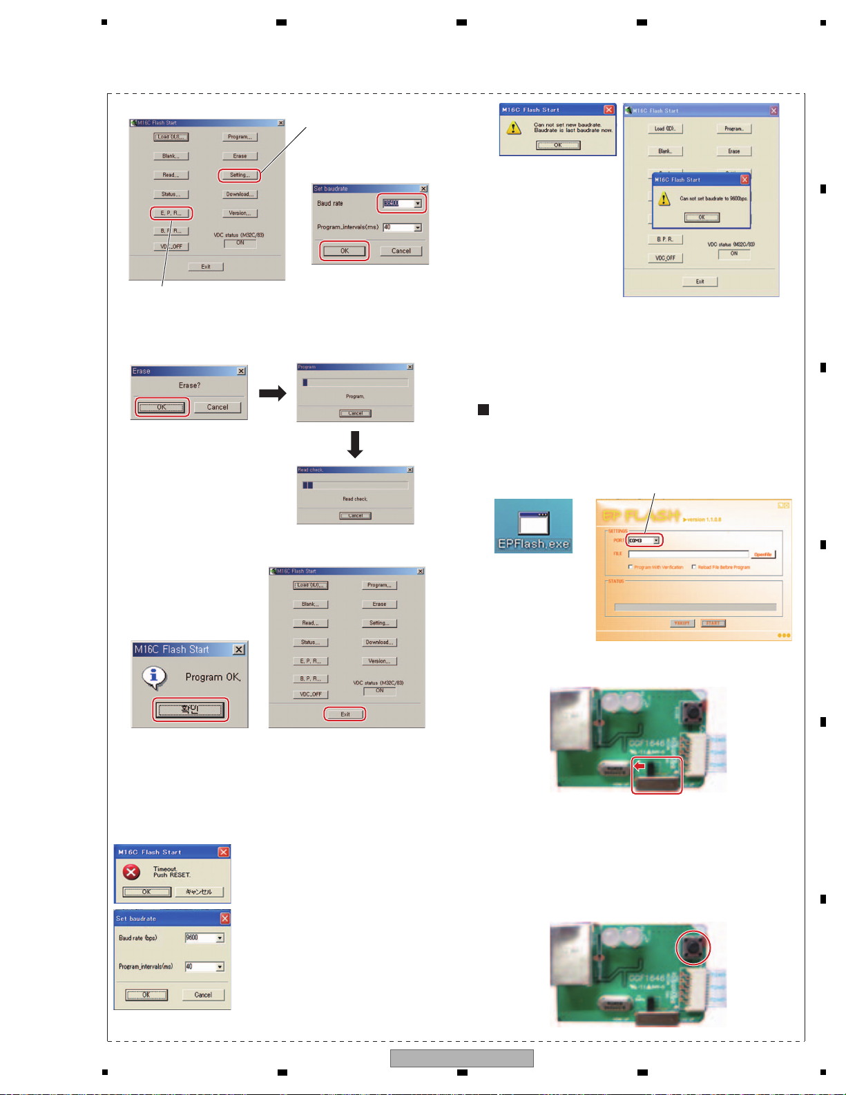
5
6. Update Finished MAIN microcomputer.
7. Unplug the AC cord.
Disconnect the FFC cable.
5. Set speed update and update the MCU.
Press the OK button.
Set Baud rate to 38400.
Press the OK button. Press the Exit button.
Please wait for until this window
disappears.
When the PC and the Upgrade Jig is connecting,
the COM PORT is set automatically.
Push the JIG’s RESET button during
1 sec.
Press the OK button.
Select the 9600 of the Board rate then
press the OK button
2 Update the MCU.
E.P.R=>Erase+Program+Read
2 Update the MCU
Press the E.P.R … button
1 Set speed of update.
1 Set speed of update.
Press OK button.
If the following messages are displayed, shut the update
program down, and start the update again from step 1.
for HDMI (SUB) microcomputer
8. Unplug the AC cord.
Start up the application EPFlash on the PC.
9. Select "HDMI UP" on the Upgrade Jig.
10. While holding down the tact switch of the Upgrade Jig,
press STANDBY/ON button.
After 2 or 3 seconds, release the tact switch button.
Connect the PC and the Upgrade Jig.
Connect the FFC cable. (HDMI microcomputer )
Plug the AC cord. (STANDBY mode)
6 7 8
A
B
C
D
E
5
VSX-522-K
6 7 8
F
53
Page 54

1
End the application EPFlash.
Select "VSX-522_LPP_********.hex" file to update MCU.
Rate of the progression is appeared.
When the PC and the Upgrade Jig
are connecting, the COM PORT is
set automatically.
Set Baud rate to 57600.
for CEC microcomputer
If the following messages are displayed, shut the update
program down, and start the update again from step 8.
11. Select the update file. Press the "OpenFile" button.
12. Press the "START" button to update the firmware.
14. Turn the unit off (STANDBY mode) and unplug the
AC cord.
Disconnect the FFC cable.
15. Unplug the AC cord.
Start up the application EPConsole on the PC.
16. Select "CEC UP" on the Upgrade Jig.
Connect the PC and the Upgrade Jig.
Connect the FFC cable. (CEC microcomputer )
Plug the AC cord. (STANDBY mode)
13. Update Finished HDMI microcomputer.
A
2 3 4
B
C
D
E
F
54
VSX-522-K
1
2 3 4
Page 55

5
Select "CECCore_ADDSEL(BB)_V***.hex" file to update MCU.
When the update file is selecting, the check box is
automatically on.
Rate of the progression is appeared.
PC's monitor is appeared the below display. By this display,
you understand that the PC and the product are communicating.
17. Select the update file. Press the "FILE" button. 19. Press the button.
20. Press the button to update the firmware.
21. Update Finished CEC microcomputer.
22. Turn the unit off (STANDBY mode) and unplug the
AC cord. Disconnect the FFC cable.
18. While holding down the tact switch of the Upgrade Jig,
press STANDBY/ON button.
After 2 or 3 seconds, release the tact switch button.
24. Turn the unit off.
23. Make sure that the main unit is in STANDBY mode.
Press and hold the " ENTER " and " STANDBY/ON " keys, then press the " ENTER "key to display each UCOM version.
Each time the " ENTER "key is pressed, then indications on the FL display change as follows:
If the following messages are displayed, shut the update
program down, and start the update again from step 15.
Check to the software virsion of MAIN, HDMI (SUB) and CEC microcomputers
"ENTER" "ENTER"
"ENTER"
"ENTER" "ENTER"
MAIN Ucom
MAIN Xx.xx
SUB Ucom
SUB zzz.zz
CEC
CEC Vy,yy
DSP firmware
All segments lit.
6 7 8
A
B
C
D
E
5
VSX-522-K
6 7 8
F
55
Page 56

1
[Procedures]
1. Select TV fucntion, and, with Signal select as OPTICAL1 then set the unit to STBY_Off mode.
2. Press the SPEAKERS and STANDBY/ON keys simultaneously to enter DSP UpDate mode. ("DSP UP" is displayed.)
3. When "PLAY" is displayed, playback of the .wav file starts. (Play the file only once. NEVER repeat playback.)
("PLAY" is displayed.)
4. After playback is finished and "ENTER" is displayed, press the ENTER key on the front panel. ("ENTER" is displayed.)
5. "WRITING" is automatically displayed.
6. After writing is completed, "COMPLETE" is displayed.
7. Turn the unit off then confirm that the version has been updated.
DSP firmware update
A
2 3 4
B
C
D
E
F
56
1
2 3 4
VSX-522-K
Page 57

5
(SL)
(SL)
• Adjustment points and measurement points.... see fig.1.
AMP5 ASSY
Fig.1
B
SIDE A
Adjustment
Points
Procedure
Measurement
Points
Channel
TP401 pin 1 (+)
TP401 pin 3 (–)
1 Turn on the power.
2 Perform aging for one minute.
3 Connect a digital voltmeter to the measurement point.
4 Turn the adjustment VR so that the voltage becomes
in 2.0 mV ± 0.2 mV.
(Condition : No signal and no load)
VR401
TP402 pin 1 (+)
TP402 pin 3 (–)
VR402
TP403 pin 1 (+)
TP403 pin 3 (–)
VR403
TP404 pin 1 (+)
TP404 pin 3 (–)
VR404
TP405 pin 1 (+)
TP405 pin 3 (–)
VR405
FL
FR
C
SL
SR
FL_VR401
SL_VR404 C_VR403 SR_VR405 FR_VR402
FL_TP401 SL_TP404 C_TP403 SR_TP405 FR_TP402
When any component parts which are within the red square on the following circuit diagram are replaced, the idle current
adjustment of that channel is required. (Idle current adjustment for another channel is not required.)
However, when any capacitors are replaced, the adjustment is not required.
(The following circuit diagram is for SL channel, but another channel also has same circuit diagram and same adjustment is
required)
6 7 8
8.3 IDLE CURRENT ADJUSTMENT
A
B
C
D
VSX-522-K
5
6 7 8
E
F
57
Page 58

1
NOTES: - Parts marked by “NSP” are generally unavailable because they are not in our Master Spare Parts List.
-
The > mark found on some component parts indicates the importance of the safety factor of the part.
Therefore, when replacing, be sure to use parts of identical designation.
-
Screws adjacent to b mark on product are used for disassembly.
-
For the applying amount of lubricants or glue, follow the instructions in this manual.
(In the case of no amount instructions, apply as you think it appropriate.)
Poly bag packing style
Cord AC
Tape (clear)
Dry cell batteries (AAA size IEC R03)
Sheet SP caution
Safety Brochure
Label getter “R”
Label getter “L”
1/2
2/2
2 3 4
9. EXPLODED VIEWS AND PARTS LIST
A
9.1 PACKING SECTION
B
C
D
E
F
58
1
2 3 4
VSX-522-K
Page 59

5
PACKING SECTION PARTS LIST
Mark No. Description Part No.
1 Remote Control (AXD7660) 8300766000010-IL
2 AM Loop Antenna E601019000010-IL
3 FM Wire Antenna E605010140010-IL
4 Microphone APM7010
(for Auto MCACC setup)
5Quick Start Guide 5707000006490-IL
6 Operating Instructions 6517000000500-IL
(CD-ROM)
7 Box, Gift 522CU 6007212070000-IL
8Cushion, Snow VSX-522 6230213144000-IL
6 7 8
A
9 PE, Sheet 6327040059000-IL
NSP 10 Warranty Card ARY7156
NSP 11 Label VRW1629
B
C
D
E
F
VSX-522-K
5
6 7 8
59
Page 60

1
O
Q
P
R
N
M
F
S
Nut
Nut
Clamp
9.2 EXTERIOR SECTION
A
B
2 3 4
C
D
E
F
60
1
2 3 4
VSX-522-K
Page 61

5
CONTACT SIDE
NON-CONTACT
SIDE
Silicon grease
(GEM1057)
Silicon adhesive
(GYA1011)
A
J
E
L
K
H
G
C
I
B
S
D
Heatsink
Main chassis
Sheet speaker
Stopper
×
24
6 7 8
A
B
C
D
E
F
5
6 7 8
VSX-522-K
61
Page 62

1
EXTERIOR SECTION PARTS LIST
Mark No. Description Par t No.
1 AUDIO Assy 7028071641060-IL
A
2 AMP5 Assy 7028070243010-IL
3 MAIN Assy 7028071611060-IL
4 D-MAIN Assy 7028071651010-IL
5 VIDEO Assy 7028071631010-IL
2 3 4
No. Description Part No.
Mark
46 Screw BBT40P080FTB
47 Screw BBZ30P080FTB
48 Screw BBZ30P080FTC
49 Screw BBZ30P180FTC
50 Screw BSZ30P040FTB
6 G-L Assy 7028071615060-IL
7 G-R Assy 7028071614060-IL
8 WG-B Assy 7028071617060-IL
9 WG-A Assy 7028071616060-IL
10 BRG-A Assy 7028071633010-IL
B
11 BRG-B Assy 7028071634010-IL
12 BRG-C Assy 7028071635010-IL
13 FRONT Assy 7028071621060-IL
14 INSEL Assy 7028071623060-IL
15 HP Assy 7028071622060-IL
16 MIC Assy 7028071624060-IL
17 F-USB Assy 7028071625060-IL
18 WG Assy 7028071627060-IL
19 STBY Assy 7028071632010-IL
> 20 Cord Assy L068125101710-IL
C
> 21 Power Trans 522CU 8200960611230-IL
22 Cable Flat Card 1.0 N711231712480-IL
> 23 Transistor J5011560Y0000-IL
> 24 Semi, TR/GE NPN 2SC J502396400010-IL
> 25 Transistor J5032390Y0000-IL
26 Pioneer Badge B (PLS) XAM3006
27 Sheet 1210210235000-IL
28 Cabinet VSX-522 3007212006000-IL
D
29 Front Panel 522CU 3067215481000-IL
30 Back Chassis 522CU 3207214176000S-IL
51 Screw Tapping Assy B018230141H11-IL
52 Screw, Tap Tite B020230063B10-IL
53 Screw 1500001206010-IL
54 Screw B028940101B11-IL
55 Screw 1500001456010-IL
31 Foot (PLS) 4000210391000-IL
32 Bracket 4010056906010-IL
33 Cushion 4050211605000-IL
34 Screw Cover 4050211745100-IL
35 Support 4070001601010-IL
36 USB Mic Plate 522 4470212416000-IL
37 Window 522CU Upper 5077213113080-IL
E
38 Window 522CU Lower 5077213123300-IL
39 Knob 5080212431000-IL
40 Button 5090213741100-IL
41 5 Key Button 5090214561000-IL
42 10 Key Button 5090214571000-IL
43 • • • • •
44 • • • • •
45 Screw BBT30P100FTB
F
62
1
2 3 4
VSX-522-K
Page 63

5
6 7 8
A
B
C
D
E
F
VSX-522-K
5
6 7 8
63
Page 64

1
C417
47N-K
470K
R478
680P-J
C511
R513
47K
100/16
C432
10/50
C433
2K2
R564
10/50
C541
R592
-
C506
10/50
C492 10/50
LUG401
NM
-
R406
R572
10K
C519
-
C520 -
R562
-
470K
R565
C540
220P-J
330
R590
C539
100P-J
330
R541
C505
220P-J
R593
330
C504
100P-J
R532
330
330
R530
220P-J
C494
R521
330
C493
100P-J
C465
100P-J
C457
-
R470
0
-
C470
R400
100
100P-J
C402
C403
-
R591
470K
R537
-
C542 10/50
R527
-
R533
-
10/50
C498
C499 10/50
R528
470K
R534
470K
-
R522
R523
470K
R463
10K
C476
-
1K
R462
R419
2K
R408
10K
2K
R402
C490
-
10K
R413
R465
-
C408
10/50
10/50
C460
10/50
C400
R473
0
47/10
C468
10N-K
C533
R568
10K
C522
-
47K
R481
100
R472
R469
100
R509
0
C517 -
C479
100P-J
100(1)
R588
10N-K-2012
C515
C507
10/50
ZD401
MTZ6.8B
C558-C566
-
Q428
2SK492C
1K5
R554
R539
4K7
C503
R503 0
R512
470
R491
0
C441
10N-K-2012
R589
100(1)
RT1P141C
Q426
C411
47N-K
R422
4K7
10K
R613
C475
10/50
R497
1K
C412
47N-K
C413
47N-K
C486
10/50
C485
10N-K
0
R518
C414
47N-K
C415
47N-K
R500
0
C418
47N-K
C502
220P-J
C544
220P-J
C543
100P-J
C501
100P-J
C497
220P-J
C496
100P-J
R417
100
C404
100P-J
R461
100
-
C405
Q416
INC2001AC1
R595
R594
470K
INC2001AC1
Q417
C487
-
R411
-
C467
47/10
47K
R485
R516
0
R576
10K
C534
10N-K
C512
3N3-K
R549
100K
R561
10K
R520
470
470
R517
100P-J
C482
R577
-
R477
470K
10N-K-2012
C473
4K7
R447
C546
330P-J
C547
330P-J
R551
100K
Q427
RT1N441C
1/50
C516
R542
0
C425
150N(R)-63V
47N(EB)-100V
C424
100/16
C429
100/16
C428
100/16
C431
10/50
C430
10/50
C434
8
4
5
6
3
2
1
7
AZ4580
IC403
Q425
2SK492C
470K
R610
R583
470K
10/50C462
J501
0
R405
47K
R559
10K
C448 47N(EB)-100V
R468
10K
C472
-
1K
R466
470K
R582
470K
R609
C529
10N-K-2012
C514
10N-K-2012
R538
470K
10/50
C488
10/50
C464
47K
R467
C459
10N-K-2012
C469
0
J500
0
R601
0
ZD400
MTZ6.8B
220/16(6.3*11)
C537
10N-K-2012
C528
D415
LBAS16HT1G
91K
R571
10K
R573
R574
10K
R557
91K
10K
R560
R544
1K
R540
4K7
C508
10N-K
R511 470
100P-J
C477
C480
100P-J
10K
R505
C449 22N(EB)-100V
R459
0
R479
-2012
R515
3K9
C416
47N-K
JACK402
JACK403
10/50
C489
R416
47K
10N-K-2012
C466
J502
0
R598
0
220/16(6.3*11)
C538
R548
5K6
C509
10/50
D414
LBAS16HT1G
C427
100/16
C447 150N(R)-63V
22N(EB)-100V
C423
R507
1K5
C4811N-K
C484
47P-J
JACK401
R566
10K
R569
10K
5
6
8
7
1
4 3
2
AZ4580
IC401
INC2001AC1
Q401
INC2001AC1
Q404
98
97
96
95
94
93
92
91
90
89
88
87
86
85
84
432 1
99
83
82
81
80
797877767574737271706968676665646362616059585756555453
5251
50
49
48
5678
910111213141516
1718
192021
22
35
36
37
38
39
40
41
42
43
44
45
46
47
23
242526
2728
2930
31
32
33
34
IC400
R2A15218FP
8
4
5
6
3
2
1
7
AZ4580
IC402
A
C
CP17
(FL)
(FL)
: Audio Signal Route (Front L ch)
(SL)
: Audio Signal Route (Surround L ch)
(C)
: Audio Signal Route (Center ch)
(SW)
(SW)
: Audio Signal Route (SubWoofer ch)
(TU)
: Audio Signal Route (Tuner L ch)
(TU)
(TU)
(CD)
: Audio Signal Route (CD L ch)
(CD)
(CD)
(SBL)
: Audio Signal Route (Surround Back L ch)
(FL)
(FL)
(SW)
(SL)
(C)
(SBL)
(SW)
(SW)
(SW
(SW)
(FL)
(SL)
(C)
(SW)
(SBL)
(SBL)
(SBL)(SBL)
(HP)
: Audio Signal Route (Headphone L ch)
: Audio Signal Route (L ch)
10. SCHEMATIC DIAGRAM
10.1 AUDIO ASSY
A
B
C
D
E
F
64
1
2 3 4
VSX-522-K
2 3 4
Page 65

C417
47N-K
100/16
C432
10/50
C433
R403
220K
R401
220K
R498
4K7
R506
4K7
R536
10K
470K
R531
R429
47K
OTHER 100pF/50V CH
100pF/50V CH
R500
0
C418
47N-K
C535
10N-K
C536
10N-K
R502
-
C463
10/50
C439
10/50
C420
10/50
C401
10/50
10K
R614
2K2
R570
470K
R597
C545
100N-K
0.22U/25V
C500
C478 0.22U/25V
R514
10K
470
R508
R471
1K5
R458
1K5
R433
1K5
R427
1K5
R404
1K5
2SK492C
Q435
R495
0
R484
47K
R474
10K
-
C564
R449
47K
R448
10K
-
C563
R435
10K
-
C561
INC2001AC1
Q407
-
C562
R420
10K
R421
47K
-
C560
R410
47K
INC2001AC1
Q402
-
C559
R409
10K
R488
1K
-
C554
-
C555
R423
10K
R487
1K
R499
0
1/50
C444
C442
100P-J
R596
220
C550
82P-J
5K6
R493
220
R586
C551
82P-J
SYXCN5
JXCN
R543
0
470/16
C437
470/16
C440
-
C556
-
C557
10/50
C434
C454
10/50
C406
10/50
C446
10/50
1K5
R415
R444
1K5
R496
0
D416
LBAS16HT1G
D417
LBAS16HT1G
Q433
2SK492C
R460
10K
INC2001AC1
Q413
-
C565
R464
47K
R428
10K
INC2001AC1
Q405
INC2001AC1
Q410
220K
R475
220K
R476
R414
10K
INC2001AC1
Q415
R504
0
C438
100P-J
C421
220P-J
5K6
R490
C410
220P-J
10N-K-2012
C569
R425
10K
10K
R424
470K
R501
***************************************
***************************************
C416
47N-K
C570
CH10P-D
C548
CH10P-D
J402
NM
J416
0
J415
0
Q434
RT1N441C
470K
R567
C518
1/50
R600
10K
Q429
RT1P141C
R599
100
C436
1/50
C443
1/50
R535
470
1/50
C422
Q419
RT1P141C
INC2001AC1
Q418
R436
47K
R529
0
R489
22K
R587
33(1)
C553
100P-J
C568
10N-K-2012
33(1)
R510
C407,C409,C419,C426,C435
ALL DESTINATION:100pF/50V CH
1K5
47P-J
C125Z2-17
CN402
C549
CH10P-D
C571CH10P-D
RT1P141C
Q432
Q421
RT1P141C
INC2001AC1
Q414
R602
0
INC2001AC1Q406
C552
100P-J
22K
R492
Q422
INC2001AC1
INC2001AC1
Q420
4 3 126 578910111213
CN400
2.0MM-13P
324
5
6 8
7
1
IC406
AZ4580
10 8 6 4 2
3579 119
1618 14 12
111317 15
CN403
C125Z2-19
C409
100P-J
100P-J
C419
100P-JC426
C407
100P-J
100P-J
C435
98
97
96
95
94
93
92
91
90
89
88
87
86
85
84
432 1
99
83
82
81
80
79787776757473
5678
A
A
AUDIO ASSY
(7028071641060-IL)
J
CP403
K
CP402
B
1/2
CP401
-
When ordering service parts, be sure to refer to "EXPLODED VIEWS and PARTS LIST" or "PCB PARTS LIST".
-
The > mark found on some component parts indicates the importance of the safety factor of the part.
Therefore, when replacing, be sure to use parts of identical designation.
-
: The power supply is shown with the marked box.
(CD)
(FL)
(SL)
(C)
(SW)
(SBL)
(FL)
(FL)
(SL)
(SL)
(C)
(C)
(SW) (SW)
(SW)
(SW)
(SW)
(SW)
(SBL)
(SBL)
(SBL)
(HP)
(HP)
(HP)
(HP)
(HP)
(HP)
5
6 7 8
A
B
C
D
E
F
65
5
VSX-522-K
6 7 8
Page 66

1
ALL
100P/100V
100P/50V
C441,C457,C473
C489,C505
100P/100V
C534,C552
C536,C558
C523,C549,C524,C555
C529,C550,C532,C557
B
1/2
B
1/2
AMP5 ASSY (7028070243010-IL)
A
CN400
B
2/2
(FL)
(FL)
(FL)
(SL)
(SL)
(C)
(C)
(C)
(C)
10.2 AMP5 ASSY (1/2)
A
2 3 4
B
C
D
E
F
66
VSX-522-K
1
2 3 4
Page 67

5
B
1/2
C
CN1
C
CN3
B
2/2
D
4/4
CP2005
(FL)
: Audio Signal Route (Front L ch)
(SL)
(SL)
: Audio Signal Route (Surround L ch)
(C)
: Audio Signal Route (Center ch)
(FL) (FL)
(FL)
(SL) (SL)
(C) (C)
(C)
(C)
6 7 8
A
B
C
D
5
6 7 8
VSX-522-K
E
F
67
Page 68

1
ALL
100P/100V
C539,C553,C542,C563
C544,C554,C547,C564
B
2/2
B
2/2
AMP5 ASSY (7028070243010-IL)
B
1/2
(SL)
(SL)
10.3 AMP5 ASSY (2/2)
A
B
2 3 4
C
D
E
F
68
VSX-522-K
1
2 3 4
Page 69

5
B
2/2
B
1/2
(SL)
: Audio Signal Route (Surround L ch)
(SL) (SL)
(SL)
6 7 8
A
B
C
D
E
F
VSX-522-K
5
6 7 8
69
Page 70

1
C78
C1
47N(EB)-100V
C17
47N(EB)-100V
R641
0
C78
0.1uF
100N-K
C72
10N-K
C108
C57
10/50
C70
-
C69
-
0.1uF
X7R
C31 1N-K
C33 1N-K
827/8
S
C82
47N(EB)-100V
C83
47N(EB)-100V
C75
-
R32
-
C79
-
R26
R27
0R22(1)
1M-3216
R79
GBJ1006
D7
R5
10(1)
10(2)
R6
D11
1N4007
D12
1N4007
LOW
R36
47K(1/4)
R7
10(1)
R8
10(2)
C4
47N(EB)-100V
R11
10(1)
R10
10(2)
C12
47N(EB)-100V
R12
10(2)
C85
1000/25(10*20)
L6
SP-2507
R13
10(1)
C22
47N(EB)-100V
R14
10(2)
TO CHASSIS
TO CHASSIS
C107
RB551V-30
D27
D25
RB551V-30
C96
10N-K
R17
10(1)
C25
47N(EB)-100V
R16
10(2)
NM
C23
R75
6K8-3216
1M-3216
R71
RB551V-30
D26
C26 1N-K
C34 1N-K
C30 1N-K
C29 1N-K
C32
1N-K
10
R24
DZ1
MTZ3.3B
R23
10
R41
0R22(1)
R42
0R22(1)
R640
0
GND2
100N(R)-250V
C65
SP-2507
L1
D10
1N4007
D13
1N4007
R35
47K(1/4)
C71
-
RLY2
HL3-2A-12S
SP-2507
L3
C77
10N-K
C74
10N-K
L4
SP-2507
RLY3
HL3-2A-12S
RB551V-30
D28
L7
SP-2507
RLY6
HL3-2A-12S
C89
100/16(6.3*11)
C88
100/16(6.3*11)
100/6.3(6.3*5)
C90
C95
10N-K
C105
10N-K
C28 1N-K
C27 1N-K
R30
2K2(1)
100/25(6.3*11)C53
KDS4148U
D6
2K2(1)
R28
C112
10N-K
Q13
RT1N237C
R37
10K
D5
KDS4148U
2
15 39 713 11
6 481012
CP605
C125Z1-13
R
FROM MAIN TRANS
TO CHASSIS
SPEAKER TERMINAL
TO CHASSIS
D16
-
47N(EB)-100V
C81
C84
4700/25(16*31.5)
C76
6800/16(16*31.5)
R31
0R22(1)
D9
KBPC604-6A
1 2 3 54
CN1
C67
100N(R)-250V
SP-2507
L2
R9
10(1)
C9
47N(EB)-100V
C13NMC10
NM
C106
-
D15
-
C87
10N-K
C86
10N-K
10N-K
C93
330(2)
R47
D14
-
R72
1M-3216
D18
-
1 32
CN2
5 6 7 8 9 104321
CN3
10(1)
R15
10(2)
R18
C20
NM
C21
10N(EB)-100V
C24
10N(EB)-100V
OPEN
R74
NM(3216)
CN6
1
234
2.5mm 4P
CN5
RT
Q6
RT1P237C
1 32
CP3
5267-03A
31 2
CP1
35328-0360
R48
1M-3216
D4912
KBPC604-6A
C61
100N(EB)-100V
C68
100N(R)-250V
C66 100N(R)-250V
C55
6800/63(30*40)
6800/63(30*40)
C58
6800/16(16*31.5)
C73
10(1)
R25
L5
SP-2507
RLY4
HL3-2A-12S
C14
10N(EB)-100V
C11
10N(EB)-100V
C94
10N-K
IC1
KIA7812API
IC3
KIA7805API
KIA7912PI
IC2
IC5
KIA7812API
RLY5
HL3-2A-12S
NM(3216)
R73
R29
2K2(1)
12345
35328-0360
CP2
100/16(6.3*11)
C92
C64
100N(EB)-100V
C5NMC2NMC7
NM
C18NMC15
NM
922L/4
CUX/F
C6
10N(EB)-100V
C8
10N(EB)-100VC310N(EB)-100V
C19
10N(EB)-100V
C16
10N(EB)-100V
C
C
MAIN ASSY (7028071611060-IL)
B
1/2
CP402
B
1/2
CP403
D
2/4
CP2004
(FL)
(FL)(FL)
(SL)
(SL) (SL)
(C)
(C)
(C)
(SBL)(SBL)
(SBL)
(SBL)
(SBL)
10.4 MAIN ASSY
A
B
C
2 3 4
D
E
F
70
1
2 3 4
VSX-522-K
Page 71

5
6K8
R75
TU_L
/RST
C62
-
R43
-
GND
INT
/SEN
R56
-
C57
10/50
2N2-KC98
100/10C99
827/822/522
SYX/JX
1M
R48/R71
(3216) (3216)
1M
NMC614
0-1608
R82
OPEN OPEN10OPEN
DZ1
MTZ3.3B
R23
10
C113
4N7-K
C59
10N-K
R22
10
J13
0
-
J7
R44
-
R63
OPEN
R61
OPEN
R62
OPEN
Q3
RT1P237C
C60
-
R59
10K
R60
27K
R50
51K
R51
51K
R49
51K
C102
1/50
R65
10K
Z24
MTZ16B
Q2
RT1P237C
R608R
1K
1KR608L
C608NMC610
NM
R52
2K2
4N7-K
C611R
NM
C635
C636
NM
0-1608
R83
NM
C613
NM
C611
NM
R636
R84
0-1608
BD3580
BEAD601
NM
R635
Q14
KTC3198Y
R55
-
C100
10N-K
KDS4148U
D6
2K2(1)
R28
C112
10N-K
Q13
RT1N237C
R37
10K
D5
KDS4148U
2
15 39 713 11
6 481012
CP605
C125Z1-13
D8
1SS133T
RT1N237C
Q12
R38
10K
RT1N237C
Q11
R39
10K
D23
1N4007
RT1N237C
Q10
R40
10K
Z25
MTZ16B
R66
4R7(1)
Q17
KSA916Y
RT1N237C
Q9
R45
10K
100N-K
C612
C611L
4N7-K
2
1 1311
141210
9753
864
15
CP17
C125Z1-15
1022/42/822:11P
10
11 579
8 6 4 2
3 1
C125Z1-11
CP9
R53
33K
KSA992F
Q16
10
11 579
8 6 4 2
3 1
CP15
C125Z1-11
1235 4
CN12
10
11 579
8 6 4 2
3 1
CP16
C125Z1-11
1022/42/822:11P
468
579 3 1
2
C125Z1-09
CP8
1
246
357
CP13
C125Z1-7
468
579 3 1
2
C125Z1-09
CP14
R72/R79
(3216)
TU_R
VCC_5V
SCLK
R74
1 234
5267-04A
CN6
1
234
2.5mm 4P
CN5
Q5
RT1P237C
Q6
RT1P237C
R58
27K
C101
330/63(12.5*20)
1/50
C103
R20
10
R21
10
C609R
10/50(5*7)
SDIO
NM-1608
R637
10/50(5*7)C609L
C607 10N-K
R54
100K
R638
NM-1608
R46
-
VIDEO B'D
R73
R29
2K2(1)
D4
KDS4148U
R64
22(1/4)
D2
KDS4148U
D3
KDS4148U
C609
10N-K
Q15
KTC3198Y
1234568 79
PACK601
RT1P237C
Q4
1022/42/822:CPU B'D
522:BRIDGE3 B'D
922L/42/822/522
CUX/FLX/PWX/AX
C
A
CN401
L
CN13
L
CN11
L
CN16
E
CN9
CP2004
(TU)
(TU)
(TU)
(TU)
(FL)
: Audio Signal Route (Front L ch)
(SL)
: Audio Signal Route (Surround L ch)
(C)
: Audio Signal Route (Center ch)
(TU)
: Audio Signal Route (Tuner L ch)
(SBL)
: Audio Signal Route (Surround Back L ch)
: Video Signal Route (Y)
(Y)
: Video Signal Route
: Video Signal Route (Cb)
(Cb)
: Video Signal Route (Cr)
(Cr)
(Y)
(Cb)
(Cr)
6 7 8
A
B
C
D
E
F
71
VSX-522-K
5
6 7 8
Page 72

1
D2001
-
-
D2000
-
D2013
-
D2012
-D2025
R2013
5K6
-D2024
R2012
5K6
-
D2037
-
D2036
R2027
-
C2010 47/16-Z8156
R2041
470
R2476
0
R2060 2K
R2120 0
R2063
47
R2062
100
R2066
100
C2026
100N-K
-
D2003
-D2002
D2015
-
-D2014
-
D2027
-
D2026
D2039
-
-
D2038
R2028 47K
C2011
100N-K
R2040
2K
R2053
2K
R2069 0
R2007
1K
R2014
5K6
R2017
-
C2156
4N7-K
R2042
1K
R2047
100
R2045
100
R2003
0
R2002
0
Q2002
RT1N141C
-D2005
-D2009
R2001
0
Q2001
RT1N141C
-D2004
-D2008
R2000
0
Q2000
RT1N141C
R2022
-
R2023
-
R2020
-
R2021
-
-
D2029-D2021-D2033
-D2017
R2018
-
-D2028
-D2020
-D2032
-D2016
R2016
-
R2026
-
R2025
-
R2024
-
R2034
10K
R2033
10K
R2036
10K
R2038
-
R2037
-
ZD2005
-
ZD2004
-
C2009
100N-K
R2043
47K
R2049
100
R2048
100
R2046
100
R2044
100
R24770R2475
0
C2014
100N-K
C2343
100P-J
R2061
1M
R2056
0
R2058 4K7
R2059
2K
R2051 10
R2119 0
C2017
100N-K
C2016
100N-K
R2065
47K
C2023
100N-K
C2333
-
R2064
100
R2067
100
2.2/
1 3 4 5 6 8 10 12 14 16 182
21
117 9 1913 15 17
22
JACK2001
AD3PBI19GO-REV.B
D2007
-
-
D2011
-D2006
-D2010
R2006
1K
R2005
1K
R2004
1K
-
D2031
D2023
-
-
D2035
-
D2019
R2015
5K6
-
D2030
-D2022
-
D2034
-
D2018
R2019
-
R2035
10K
R2032
10K
R2039
2K
1N-K
C2105
C2346
4N7-K
C2347
4N7-K
C2013
100N-K
C2015
100N-K
C2019
22P-J
C2348
4N7-K
R2054
10
R2057
10
R2055 4K7
R2052
2K
C2018
100N-K
C2331
100P-J
C2321
100N-K
C2349
4N7-K
C2025
100N-K
C2109
-
C2024
100N-K
C2
100
C2
1N
1 3 4 5 6 8 10 12 14 16 182
21
117 9 1913 15 17
22
JACK2002
AD3PBI19GO-REV.B
1 3 4 5 6 8 10 12 14 16 182
21
117 9 1913 15 17
22
JACK2000
AD3PBI19GO-REV.B
Q2003
RT1N141C
C2012
47/16-Z8156
1 3 4 5 6 8 10 12 14 16 182
21
117 9 1913 15 17
22
JACK2003
AD3PBI19GO-REV.B
CB2000
0
C2002
100N-K
C2275
-
C2001
100N-K
C2007
100N-K
C2006
100N-K
Q2007
RT1N441C
R2011
10K
Q2006
RT1N441C
R2030
47K
Q2005
RT1N441C
R2029
47K
Q2004
RT1N441C
ZD2003
-
CB2001
0
C2005
100N-K
C2330
1N-K
C2003 100N-K
C2004
100N-K
C2329
1N-K
C2261
100P-J
C2008
100N-K
C2112
1N-K
C2113
100P-J
C2104
1N-K
XTAL2000
24MHZ-15pF
R2070
10K
C2022
100N-K
R2084
-
R2050
10
R2071
100
R2068
10K
R2031
47K
R2010
10K
R2009
10K
R2008
10K
C2345
4N7-K
C2000
100N-K
C2073
100N-K
C2021
20P-J
1 2 3
464748
49
50
51
52
53
54
55
56
57
58
59
60
61
62
63
64
4 5 6
7 8
9 10 111213 141516
17
18
19
20
21
22
23
24
25
26
27
28
29
30
31
32
33
34353637
3839
404142434445
IC2001
EPF021A
P21
P22
P23
P24
P25
P26
P27
TIMO
TIMI
P10
P11
P12
P13
P70
P31
P30
VDD
P35
P34
P33
P32
VSSA
ADC1
ADC0
VDDA
DP
DM
XO
RSTb
opm0
GND
RMC
P50
P51
P52
P53
P54
P55
P56
P57
P00
P01
P02
P03
P04
P05
P06
P07
P60
P61
P62
P63
VDD
VSS
XIN
VDD
VSS
SPI_CLK
SPI_DO
P8(0)
P8(1)
P41
P40
P71
C2108
4N7-K
C2020
100N-K
C2332
1N-K
1
234567891011121314151617181920212223242526272829303132
3334353637383940414243444546474849505152535455
56
105
106
107
108
109
110
111
112
113
114
115
116
117
118
119
120
121
122
123
124
125
126
127
128
IC2000
EP94A1K
PVDD
AVDD
RXCORXCO+
AVSS
RX00RX00+
AVDD33
AVSS
RX10RX10+
AVDD
RX20RX20+
AVSS
PVDD
AVDD
RXC1RXC1+
AVSS
RX01RX01+
AVDD33
AVSS
RX11RX11+
AVDD
RX21RX21+
AVSS
RXC2+
AVSS
RX02-
RX02+
AVDD33
AVSS
RX12-
RX12+
AVDD
RX22-
RX22+
AVSS/PVSS
PVDD/AVDD
RXC3-
RXC3+
AVSS
RX03-
RX03+
AVDD33 VDD
SPDIF
VSSE
VSS
MCLK
IIS_SCLK
IIS_WS
IIS_SDO
VSS
DDCO_SDA
DDCO_SCL
PH1
PH2
VSS
VDD
VDD
SDA
SCL
VSS
VDDE
reserved
NCNCNC
PVSS
VDDE
RXC2-
AVDD
PVDD
AVSS
EXT_RES
D
1/4
D 4/4 D 4/4 D 4/4
10.5 D-MAIN ASSY (1/4)
A
B
C
2 3 4
D
E
F
72
VSX-522-K
1
2 3 4
Page 73

R2060 2K
R2120 0
R2063
47
R2062
100
R2066
100
C2026
100N-K
C2035
-
C2206
4N7-K
C2053100N-K
C2062
10/16-Z8154
C2065 1N-K
R2069 0
CB2002
0
R2075
47K
C2336
82P-J
C2049
100N-K
CB2014
0
CDS2C05HDMI1D2046
CDS2C05HDMI1D2048
CDS2C05HDMI1D2050
CDS2C05HDMI1D2052
R2101
0
+5V
DDC_SDA
TXC-
TXC+
TX0-
TX0+
TX2-
TX2+
R2058 4K7
R2119 0
R2065
47K
C2023
100N-K
C2333
-
R2064
100
R2067
100
ZD2006
UDZ5.1B
R2072
10
R2073
1K
R2233
-
C2342
1N-K
C2028
100N-K
C2029
2.2/50-Z8154
C2030
4N7-K
R2074
2K2
C2036
20P
C2034
22P-J
XTAL2001
18M432MHZ-15pF
R2076
0
CB2010
0
C2042
100N-K
C2047
100N-K
CB2006
4R7
C2046
100N-K
C2339
1N-K
C2043
10/16-Z8154
CB2005
0
CB2004
0
C2208
4N7-K
R2086
27K
R2087
10
C2051
1N-K
R2091
47K
R2088
10K
R2089
10K
R2090
10K
R2093
10
R2094
47K
C2061
1N-K
C2064
100N-K
C2066
10/16-Z8154
C2068
-
R2097
51
1
2
4
3
L2002
-
1
2
4
3
L2003
-
R2102 0
1
2
4
3
L2000
-
R2105
1K8
CB2011
0
R2099
-
C2071
1000N-K
R2103
0
R2108
-
C2070
-
R2107
0
C2201
82P-J
GND
DDC_SCK
TX1-
TX1+
10
C2321
100N-K
C2349
4N7-K
C2025
100N-K
C2109
-
C2024
100N-K
C2027
100N-K
C2031
100N-K
C2334
1N-K
C2335
100P-J
C2032
100N-K
R2079
-
R2080
270
C2353
-
C2341
1N-K
R2078
1M
C2041
100N-K
C2337
100P-J
C2044
1/50-Z8155
C2052
10N-K
C2054
100N-K
C2057
10/16-Z8154
C2056
100N-K
C2050
10/16-Z8154
C2058
47/16-Z8156
C2060
10N-K
R2092
10
R2134
0
R2098
4R7
C2069
1000N-K
CDS2C05HDMI1D2045
1
2
4
3
L2001
-
1 2 3
45
OUT
GND
SETON
IN
IC2006
-
CDS2C05HDMI1D2053
CDS2C05HDMI1D2049
CDS2C05HDMI1D2051
CDS2C05HDMI1D2047
CB2012
0
CB2013
0
C2055
100/6.3-Z8156
C2059
1/50-Z8155
1345681012141618 2
21
11 7919 131517
22
JACK2004
AD3PBI19GO-REV.B
CB2008 0
C2340
82P-J
R2471
0
R2083
100
R2082
100
UTILITY/HEAC+
TX1 SHIELD
R2070
10K
C2022
100N-K
R2071
100
R2068
10K
C2048
1000N-K
C2038
47/16-Z8156
LBAS16HT1G
D2044
R2085
10
R2077
47
R2457
0
R2188
270
CB2009
0
C2205
82P-J
C2045
100N-K
C2338
1N-K
C2202
82P-J
CB2007
0
C2037
100N-K
R2226
0
R2234
0
R2290
0
R2309
0
R2081
100
C2039
100N-K
C2040
1/50-Z8155
CB2003
0
R2096
51
R2095
0
R2106
1K8
C2072
1N-K
R2100
-
R2104
0
CE_REMOTE
HP_DET/HEAC-
TX0 SHIELD
TXC SHIELD
TX2 SHIELD
1234
5 6 7 8
IC2002
VCC
2Y
3A
1Y
GND
2A
3Y
1A
C2021
20P-J
7 8
9 10 111213 141516
17
18
19
20
21
22
23
24
25
26
27
28
29
30
31
32
33
34353637
3839
404142
IC2001
EPF021A
VDD
P35
VSSA
ADC1
ADC0
VDDA
DP
DM
XO
RSTb
opm0
GND
RMC
P50
P51
P52
P53
P54
P55
P56
P57
P00
P01
P02
P03
P04
P05
P06
P07
P60
P61
P62
P63
VDD
VSS
XIN
C2108
4N7-K
C2020
100N-K
C2332
1N-K
C2033
100N-K
1098765432
1
11
12
1314151617
181920212223
24
IC2003
EPF011C
RXD
TXD
SCL
SDA
RSTb
IO3
IO2
INTb
BIST
A6
CECO
CECin
DDC_SCL
DDC_SDA
XO
VDD
VSS
XIN
VSS
OP_MODE
VDD
A2A1A0
R2135
0
C2067
1000N-K
C2063
100/6.3-Z8156
CDS2C05HDMI1D2054
12
3
4 5
CNT
GND
NC
VO
VI
IC2004
NJM2831F33
1
2
3
4
5
IC2005
S-1170B18-UC
ON/OFF
VSS
NC
VOUT
VIN
45464748495051525354555657585960616263
64
65 66 67 68 69 70 71 72 73 74 75 76 77 78 79 80 81 82 83 84 85 86 87 88 89 90 91 92 93 94 95 96
979899
100
101
102
103
104
105
106
107
108
109
110
111
112
113
114
115
116
IC2000
EP94A1K
RX12+
AVDD
RX22-
RX22+
AVSS/PVSS
PVDD/AVDD
RXC3-
RXC3+
AVSS
RX03-
RX03+
AVDD33
AVSS
RX13-
RX13+
AVDD
RX23-
RX23+
AVSS
TX0-
TX0+
TX1-
TX1+
AVDD18
TX2-
TX2+
AVSS
AVDD33
VDD
NC
DDC3_SDA
DDC3_SCL
DDC2_SDA
DDC2_SCL
DDC1_SDA
DDC1_SCL
VSSE
DSD3R
DSD3L
IIS_SD3
IIS_SD2
IIS_SD1
XIN
XOUT
VDDE
VDD_PLL
PLL_XFC_A
VSS_PLL
VSS
VDD
VDD
SPDIF
VSSE
VSS
MCLK
IIS_SCLK
IIS_WS
IIS_SDO
VSS
DDCO_SDA
DDCO_SCL
PH1
SWING
INTb
EXT_RSTb
A_MUTE
VSS
AVDD18
TXC+
TXC-
AVSS
PVDD18
D
1/4
D
1/4
D-MAIN ASSY (7028071651010-IL)
D 4/4 D 2/4 D 4/4 D 2/4
5
6 7 8
A
B
C
D
E
F
VSX-522-K
5
6 7 8
73
Page 74

1
C2081
-
C2116
GRM31CB31C226KE15L
C2125
4N7-K
C2115
GRM31CB31C226KE15L
Min.25V
R2136
10
D2055
LBAS16HT1G
C2074
22P-J
C2075
10N-K
R2109
4K7
C2089
330P-J
C2087
330P-J
C2084
10N-K
C2080
22P-J
R2458
0
R2113
10K
R2114
2K2
C2101
100N-K
C2103
CH2N2-J
C2100
100N-K
C2102
3N3-K
R2462
-
R2133
750
R2132
18K-F
R2137
10
R2129
10K-F
R2465
0
R2122
100K
R2139
1M
R2140
47K
R2138
1M
C2117
1N-J
R2141
47K
R2463
-
C2114
330P-J
C2119
10N-K
C2354
82P-J
R2466
0
C2121
10/16-Z8154
R2464
-
R2467
0
C2076
330P-J
L2004
BD121T
L2005
2.2UH
C2082
1N-J
C2085
10P-D
C2083
330P-J
R2111
100
L2006
0
C2093
GRM31CB31E106KA75L
C2095
GRM31CB31E106KA75L
Q2026
-
C2090
22P-J
R2118
11K
R2125 5K6-F
R2117
7K5
R2126 7K5-F
R2131
7K5-F
C2111
GRM31CB31C226KE15L
Q2028
-
R2130
330
R2128
10K-F
C2118
1N-J
Q2030
-
C2120
-
L2009
0
Q2032
-
C2124
CH2N2-J
C2350
82P-J
10N-K
C2123
C2094
GRM31CB31E106KA75L
C2091
GRM31CB31E106KA75L
C2110
GRM31CB31C226KE15L
R2127
300K
R2110
75
C2092
100N-K
R2116
0
L2036
0
C2099
100N-K
R2115
0
C2088
100N-K
L2007
22UH
L2035
0
C2097
100N-K
C2096
10P-D
Q2027
-
Q2029
-
R2316
-
R2112
100K
R2124
33
C2107
1000N-K
C2106
47P-J
Q2031
-
Q2033
-
R2143
33
R2142
100
L2010
BD121T
10
8
64
2
3
5 7
91
1
11
CN2003
C125Z2-19
D2057
RB501V40
D2056
RB501V40
R2145
100
C2077
100P-J
C2079
100N-K
JACK2005
RCA-107A
JACK2006
JSR1165-C
L2008
22UH
C2098
10P-D
7
5
6
2
9
3
4
11
8
1
10
12
IC2008
BD9328
SS
EN
COMP
FB
VIN
BSTSWGND
7 5
6
2
9
3
4
11
8
1
10
12
IC2007
SS
EN
COMP
FB
VIN
BST
SW
GND
BD9329
R2123
33
C2322
100N-K
C2323
100N-K
R2121
2K2
C2122
100N-K
C2324
100N-K
C2325
100N-K
R2144
100
34 12
CP2004
5268-04A
C2078
47/16-Z8156
141312
3 2 1
111098
7 6 5 4
IC2009
74VHCU04
4Y
4A
5Y
5A
6Y
6A
VCC
GND
3Y
3A
2Y
2A
1Y
1A
AXCN(CHINA):NM
C2086
0.1/50-Z8154
D
2/4
C
CN5
J
CP2
D 1/4D 4/4
(FL)
(SL)
(FL)
(SL)
10.6 D-MAIN ASSY (2/4)
A
B
2 3 4
C
D
E
F
74
VSX-522-K
1
2 3 4
Page 75

5
R216310R2166
10
H
L
C2125
4N7-K
R2164
10K
R2157
47
C2140
330P-J
R2176
0
C2126
-
L2011
-
R2154
12K-F
R2160
47K
C2137
10N-K
R216110R2165
10
R2159
4K7
R2158
4K7
R2156
10K
R2162
10K
R2174
33
R2173
33
R2167
0
C2138
330P-J
C2143
100P-J
R2177
0
C2141
-
R2175
0
C2146
22P-J
DSD
C2147
22P-J
C2350
82P-J
C2128
100/6.3-Z8156
C2132
10000N-K
R2155
47K
L2013
2.2UH
R2171
4K7
R2172
4K7
C2145
100/6.3-Z8156
R2184
47
C2142
100P-J
R2186
C2148
10000N-K
C2150
10000N-K
C2144
100N-K
R2153
100
*HD_AUDIO/DSD SELECT
R2179
33
R2185
10
8
64
2
3
5 7
91 19
16
18
14
12
11 13 17
15
R2145
100
C2127
-
R2152
100
R2168
10K
R2150
100
R2148
100
R2147
100
R2146
100
C2130
10N-K
C2131
220/6.3-Z8157
C2155
330P-J
C2135 100/6.3-Z8156
C2133
10N-K
C2134
-
HD_AUDIO
R2180
33
R2178
33
R2181
33
XTAL2002
24.576M(15p)
L2014
LBC2012T-4.7UH
C2139
10N-K
L2015
BD121T
R2187
L2016
-
R2144
100
R2151
100
C2129
10N-K
C2136
10N-K
R2149
100
R2182
33
R2183
33
C2149
100N-K
R2169
0
L2012
LBC2012T-4.7UH
R2170
0
10
11121314
15
16
5
4
321 6
9
8
7
IC2010
TC74VHC157FK
A/B
1A1B1Y2A2B2YGND
VCC
OE
4A
4B4Y3A3B3Y
123456789101112
717273747576777879
80
49 50 5152 53 5455 56 57 58 59 60
616263646566676869
7031
323334353637383940
41 42 4344 45 46 47 48
1314151617181920
212223242526272829
30
IC2011
AK4588
CAD1
RX7
I2C
DAUX2
VIN
MCLK
TX0
RX6
TVDD
DVDD
DVSS
XTO
XTI
TEST3
MCKO2
MCKO1
COUT
UOUT
RX3
PVSS
R
PVDD
RX4
TEST2
RX5
CAD0PDN
VOUT
SDTO2
BICK2
LRCK2
SDTO1
BICK1
XTL0
CSN
SDTI4
SDTI3
SDTI2
SDTI1
XTL1
INT1
NC
NC
RX0
NC
DZF1
DZF2
NC
RIN
RX1
NC
MASTER
LOUT4
ROUT4
LOUT3
NC
AVSS
AVDD
VREFH
VCOM
ROUT1
LOUT1
ROUT2
LOUT2
41.ROUT3(C)
61.RX2
60.TEST1
BOUT
TX1
80.INT0
21.CCLK/SCL
22.CDTI/SDA
20.CDTO
19.LRCK1
DAUX1
NC
NC
NC
LIN
NC
D
2/4
D
2/4
D-MAIN ASSY (7028071651010-IL)
J
CP2003
D 1/4
D 3/4
(FL)
: Audio Signal Route (Front L ch)
: Audio Signal Route (L ch)
(SL)
: Audio Signal Route (Surround L ch)
(C)
: Audio Signal Route (Center ch)
(SW)
: Audio Signal Route (SubWoofer ch)
(SBL)
: Audio Signal Route (Surround Back L ch)
(FL)
(SL)
(C)
(SW)
(SBL)
(FL)
(SL)
(C)
(SW)
(SBL)
(FL)
(SL)
(C)
(SW)
(SBL)
6 7 8
A
B
C
D
5
VSX-522-K
6 7 8
E
F
75
Page 76

1
R2231
47
R2236
47
R2244
-
R2200
100
R2197
0
R2196
0
C2196
100N-K
C2195
1N-K
C2191
330P-J
R2379
47K
C2152
10/16-Z8154
R2190
47K
C2157
-
C2154
220/6.3-Z8157
C2153
10N-K
R2199
33
R2198
0
C2159
10N-K
R2483
0
C2158
10N-K
R2203
0
C2162
18P-J
C2170
18P-J
L2024
0
L2023
0
C2175
10000N-K
C2169
1N-K
C2167
1N-K
L2026
0
L2025
0
R2222
100
R2219
100
C2199
100N-K
R2213
47
R2214
47
C2197
100N-K
R2223
47
C2193
100N-K
C2185
10P-D
C2183
1N-K
R223247R2235
47
R2229
47
C2207
100N-K
R2239
-
R2240
-
47
C2210
C2151 10N-K
Q2035
RT1N141C
L2020
BD121T
R2204
0
C2171
100/6.3-Z8156
C2168
1N-K
C2172
100/6.3-Z8156
R2220
100
R2221
100
C2198
330P-J
R2212
47
C2184
1N-K
C2194
100N-K
100N-K
C2190
C2181
1N-K
C2182
1N-K
R2247
-
C2160
220N-K
R2482
0
R2193
100
R2191
0
L2017 0
R2217
47
R2215
47
R2205
1M
R2211
47
R2194
100
R2227
0
R2192
47
L2018
BKP_HS101-2125
C2326
100N-K
D2058
-
R2216
47
R2218
47
R2206
470
C2180
100N-K
C2166
-
IC2015
IL1117-1.8
L2022
BKP_HS101-2125
C2173
100/6.3-Z8156
C2178
100N-K
L2021
BKP_HS101-2125
C2165
10000N-K
R2210
47
R2209
47
C2163
-
C2164
-
R2237
4K7
R2479
1K5
C2204
100N-K
C2209
1N-K
C2192
100N-K
C2189
100N-K
C2188
1N-K
C2200
220N-K
C2203
100N-K
R2468
-
Q2034
FDC608PZ
IC2013
SA1117D-1.2
XTAL2004
24M(12P)
R2208
-
R2207
47K
C2186
330P-J
C2174
100/6.3-Z8156
C2179
100N-K
C2176
100N-K
C2177
100N-K
D2065
-
C2187
100N-K
2
1
CP2007
-
C2161
100/6.3-Z8156
10 11 1213 14 15 16
5 4 3 2 16
9
8 7
IC2014
A
/B
1A
1B
1Y
2A
2B
2Y
GND
VCC
OE
4A
4B
4Y
3A
3B
3Y
74LCX257MTCX
176
174
172
170
168
169
166
167
165
163
161
159
157
155
153
151
149
150
147
148
146
144
142
140
138
136
134
1 3 579 11 12
171
173
175
164
162
156
158
160
154
152
141
143
145
139
133
135
137
132 130 128 126 124 122
42
6 8 10
131 129 127 121123125
Dvdd
SPI0_SCS[0]
SPI0_CLK
SPI0_ENA
AXR1[10]
DVdd
AXR1[6]
AXR1[8]
AXR1[7]
AFSR1
CVdd
ACLKR1
AFSX1
CVdd
CVdd
AXR1[11]
SPI1_SCS[0]
AXR1[4]
AXR1[5]
DVdd
ACLKX1
AHCLKX1
CVdd
DVdd
GP7[14]
TDO
TCK
CVdd
TDI
TMS
DVdd
TRST
RTC_CVdd
RTC_XI
CVdd
RESET
OSCOUT
OSCIN
PLL0_VSSA
PLL0_VDDA
NC
USB0_DM
USB0_DP
USB0_VDDA33
OSCVSS
SPI1_ENA
AMUTE1
AFSR0
ACLKR0
AHCLKR0
Dvdd
AFSX0
NC
USB0_VDDA18
ACLKX0
134:USB0_VDDA12
133:RSV2
USB_REFCLKIN
AXR0[11]
UART1_TXD
UART1_RXD
AXR0[8]
2:I2C0_SDA
1:AXR1[0]
3:I2C0_SCL
AXR1[1]
AXR1[2]
AXR1[3]
D
3/4
D
3/4
D-MAIN ASSY (7028071651010-IL)
D 2/4
D 4/4
D 4/4
10.7 D-MAIN ASSY (3/4)
A
B
C
D
2 3 4
E
F
76
VSX-522-K
1
2 3 4
Page 77

5
R2231
47
R2236
47
R2245
-
R2244
-
R2249
47
R225047R2252
47
R225547R225747R226147R2264
47
C2352 -
C2269
1N-K
D2267 CDS2C05HDMI1
R2286
47
R2285
47
R2282
47
R2279
47
R2278
47
R2277
47
R2275
47
R2274
47
R2273
47
R2271
47
R2270
47
R2268
47
C2250
100N-K
R223247R2235
47
R2229
47
C2207
100N-K
R2239
-
R2240
-
R2242
4K7
R2248
47
R223847R224147R2243
47
C2211
100N-K
C2210
100N-K
C2212
100N-K
C2217
100N-K
C2215
330P-J
C2216
100N-K
C2213
1N-K
C2222
100N-K
C2220
-
C2221
1N-K
C2224
100N-K
C2225
-
C2227
330P-J
C2226
100N-K
C2229
100N-K
C2228
100N-K
R2284
47
R2280
47
R2281
47
R2283
47
R2276
47
R2269
47
R2272
47
R2265
47
R2266
47
R2267
47
R2287
0
C2344
1N-K
C2328
1000N-K
C2327
-
R2291
10K
R2292
10K
C2259
100N-K
C2257
100N-K
C2254
1N-K
C2255
100N-K
C2251
100P-J
R2297
-
R2295
-
R2294
1K
R2296
1K
R2301
-
R2300
1K
R2307
0
R2306
0
R2308
0
R2247
-
R2246
47K
R225147R2253
47
R225447R225647R225947R226047R226247R2263
47
C2351 -
R2470
47K
C2256
1N-K
C2260
1N-K
C2253
100N-K
2
1 3 975
8 1064
CN2000
-
-
R2302-R2303
C2270
100N-K
C2273-C2274-C2272
100N-K
C2271
100/6.3-Z8156
D2268 CDS2C05HDMI1
1235 4
20010WS-05
CP2006
R2237
4K7
R2479
1K5
C2204
100N-K
C2209
1N-K
C2214
100N-K
C2203
100N-K
C2218
100N-K
C2242
-
C2241
100N-K
C2240
1N-K
C2239
100N-K
C2238
100N-K
C2235
100N-K
C2236
330P-J
C2232
1N-K
C2230
100N-K
C2223
100N-K
C2219
100N-K
C2249
10N-K
R2289
10K
R2288
10K
R2299
47K
R2298
-
C2252 1N-K
L2028
0
L2029
0
R2469
100
R2481
47K-F
R2480
47K-F
L2031
0
R2305
-
241
3
L2030
DLP11SN121SL2L
R2304
-
L2032
BD121T
R2310
0
D2066
-
2
1
CP2007
-
C2244
100N-K
R2258
47
R2293
47
1234
5 6 7 8
IC2019
CS#
WP#
GND
SI/SIO0
SCLK
HOLD#
SO/SIO1
VCC
W25Q32VSSIG
C2258
220/6.3-Z8157
1234
5 6 7 8
IC2024
TPS2557
GND
IN
IN
EN
OUT
OUT
LIM
FAULT
C2248
10P-D
R2311
0
123
545352
5 4678910111213141516
41 42 4344 45 46 47 48 49 50 5139 4033 34 35 36 37 3829 30 31 32
28
1718192021222324252627
IC2018
W9864G6JH-6
VDDQ
DQ0
VDD
DQ2
DQ1
DQ3
GNDQ
DQ4
VDDQ
DQ5
DQ6
DQ7
VDD
LDQM
WE
CAS
RAS
CS
BS0
BS1
A10
A0
A1
A2
A3
VDD
GND
A4
A5
A6
A7
A8
A9
A11
NC
CKE
CLK
UDQM
NC
GND
DQ8
VDDQ
GNDQ
DQ9
DQ10
VSSQ
DQ11
DQ12
VDDQ
DQ13
DQ14
GNDQ
DQ15
GND
C2243
100N-K
C2247
100N-K
C2246
100N-K
C2245
-
C2234
100N-K
C2231 100N-K
C2268
1N-K
C2264
100N-K
C2266
100N-K
C2265
-
C2237
100N-K
C2233
100N-K
C2267
1N-K
1 3 579 11 1312 15
14 16
18 20 22 24
26 28
30 323433 35
37 39
41 43
132 130 128 126 124 122 117 115 113 111 109 107 105 103 101 99 98 96 94 92 90
42
6 8 10
17
19 21
23 25
27 29 31 36 38 40 42 44
45
47
49
51
52
53
54
55
56
58
60
62
64
66
68
70
71
72
73
74
75
77
79
81
83
85
87
131 129 127 121123125 118119 114116 112 106108110 104 100102 97 95 9193
46
48
50
57
59
61
63
65
67
69
76
78
80
82
89
84
86
88
120
177
GND
IC2016
D808K013BPTP400
Dvdd
SPI0_SCS[0]
Dvdd
Dvdd
Dvdd
SPI0_CLK
SPI0_ENA
SPI1_SOMI[0]
SPI1_SIMO[0]
Dvdd
SPI1_CLK
SPI0_SIMO[0]
CVdd
EMA_OE
DVdd
CVdd
EMA_A[1]
EMA_A[3]
DVdd
EMA_A[4]
EMA_A[5]
EMA_A[6]
EMA_A[7]
EMA_A[8]
EMA_A[11]
AXR1[10]
DVdd
AXR1[6]
AXR1[8]
AXR1[7]
AFSR1
CVdd
ACLKR1
AFSX1
CVdd
CVdd
AXR1[11]
SPI1_SCS[0]
AXR1[4]
AXR1[5]
DVdd
ACLKX1
AHCLKX1
CVdd
CVdd
CVdd
CVdd
EMA_WAIT[0]
EMA_BA[0]
EMA_CS[3]
EMA_CS[2]
EMA_A[0]
EMA_A[2]
CVdd
EMA_A[9]
EMA_A[12]
DVdd
CVdd
DVdd
DVdd
DVdd
CVdd
DVdd
CVdd
CVdd
DVdd
CVdd
CVdd
DVdd
GP7[14]
TDO
TCK
CVdd
TDI
TMS
DVdd
TRST
RTC_CVdd
RTC_XI
CVdd
RESET
OSCOUT
OSCIN
PLL0_VSSA
PLL0_VDDA
NC
USB0_DM
USB0_DP
USB0_VDDA33
OSCVSS
SPI1_ENA
EMA_BA[1]
EMA_A[10]
AMUTE1
AFSR0
ACLKR0
AHCLKR0
Dvdd
AFSX0
SPI0_SOMI[0]
NC
USB0_VDDA18
ACLKX0
134:USB0_VDDA12
133:RSV2
USB_REFCLKIN
AXR0[11]
UART1_TXD
UART1_RXD
AXR0[8]
AXR0[7]
AXR0[6]
AXR0[5]
AXR0[4]
AXR0[3]
AXR0[2]
AXR0[1]
AXR0[0]
EMB_RAS
EMB_CS[0]
EMB_BA[0]
EMB_BA[1]
EMB_A[10]
EMB_A[0]
EMB_A[1]
EMB_A[2]
EMB_A[3]
EMB_A[4]
EMB_A[5]
EMB_A[6]
EMB_A[7]
EMB_A[8]
EMB_A[9]
EMB_A[11]
Dvdd
EMB_A[12]
85:EMB_WE_DQM[1]
86:EMB_CLK
87:DVdd
88:EMB_SDCKE
EMB_D[8]
EMB_D[9]
EMB_D[10]
EMB_D[11]
EMB_D[12]
EMB_D[13]
EMB_D[14]
EMB_D[15]
EMB_D[0]
EMB_D[1]
EMB_D[2]
EMB_D[3]
EMB_D[4]
EMB_D[5]
EMB_D[6]
EMB_D[7]
EMB_WE_DQM[0]
EMB_WE
EMB_CAS
EMA_WE
EMA_D[7]
EMA_D[6]
EMA_D[5]
EMA_D[4]
EMA_D[3]
46:EMA_D12]
45:EMA_D[1]
47:DVdd
EMA_D[0]
DVdd
2:I2C0_SDA
1:AXR1[0]
3:I2C0_SCL
AXR1[1]
AXR1[2]
AXR1[3]
D
3/4
Q
CN2006
D 4/4
6 7 8
A
B
C
D
E
VSX-522-K
5
6 7 8
F
77
Page 78

1
R2334
4K7
R2340 -
R2342
10K
C2283
100N-K
R2327
10K
C2276
10N-K
R2312
1K
C2278
10N-K
C2279
1N-K
R2320
47K
R2484
0
R2321
47
R2323
0
R2325
10K
R2328
10K
10K
R2329
R2330
10K
C2286
10N-K
D2060
LBAS16HT1G
R2333
1K
Q2013
RT1N237C
R2335
10K
R2337 -
R2326
10K
C2288
10N-K
R2353
R234
1K
R2313
47K
R2322
47K
C2284
330P-J
C2282
10N-K
Q2011
RT1N144C
10/16-Z8154
C2285
R2331
10K
C2287
2.2/50-Z8154
R2336
4K7
Q20
2SC30
D2059
LBAS16HT1G
R2319
0
R2318
0
R2317
0
R2344
R2351
R2350
R2348
R2493
ZD2001 UDZ3.3B
C2277
100N-K
R2314
47K
R2456
0
C2280
1N-K
C2281
100P-J
R2324
3K3
R2339
47K
R2343
R2346
R2349
R2347
R2341
10K
R2461
0
R2315
47K
14 13 12
3
21
11
10 9
8
76
54
IC2020
SN74AHCTO8-EL2
Q2010
ISA1530AC1
R2338
100K
R2332
3K3
Q2012
ISA1530AC1
D2061
LBAS16HT1G
1191715 7
91113
5
3
18 16
14610 412 8
2
20
21
2426 22
23
25
27
CN2001
C125Z2-27
1086 4
2
35
79 1
19
1618
14
12
11
1317 15
CN2002
C125Z2-19
24
1412
3 1
20 18
16
5
6
8
10
19 17
1513
7
9
11
MFI341S2162
IC2021
mode1
reset
mode0
SCL
{pin20}
{pin18}
{pin16}
{pin6}
{pin8}
{pin10}
{pin19}
{pin3}
{pin17}
{pin7}
vcc
{pin9}
{pin15}
SDA
vss
{pin1}
D
4/4
D
4/4
D-MAIN ASSY (7028071651010-IL)
L
CP2001
L
CP2002
D 1/4 D 1/4 D 1/4 D 3/4D 2/4
10.8 D-MAIN ASSY (4/4)
A
B
2 3 4
C
D
E
F
78
1
VSX-522-K
2 3 4
Page 79

5
R2334
4K7
R2340 -
R2342
10K
R2494
0
R24960R2498
0
R2434
-
R2354
10K
C2289
10N-K
C2291
10/16-Z8154
R2377
100
R237822R2384
22
R2390
10K
R2393 100
R2397
22
C2315
10N-K
R2387
100K
R2372
4K7
C2286
10N-K
D2060
LBAS16HT1G
R2333
1K
Q2013
RT1N237C
R2335
10K
R2337 -
R2326
10K
C2288
10N-K
R2353
220K
R2355
10K
R2345
1K
R2360
22
R2373
4K7
R2371
1K
R2368
10K
R2487
0
R2486
0
R2381
100
R2383
1K
R2460
22
R2386
22
R2472
0
R2396
100K
C2300
100N-K
LBAS16HT1G
D2062
R2389
10K
C2295
22P-J
R2395
-
R2399
-
R2392 10K
R2489
0
C2301 10N-K
R2411
100K
R2404
10K
R2406
22
R2495
0
R2497
0
R2407
47K
R2408
-
R2490
0
Q2018
RT1N141C
R2409
0
R2416
470K
C2303 10N-K
R2415
100
R2499
0
ZD2002
UDZ15B
R2433
Q2023
2SC3052
R2432
120K
R2421
100
R2437
10
R2474
0
R2419
-
R2420
-
R2442
Q2024
2SC3052
C2311
10N-K
R2441
120K
Q2025
2SC3052
R2446
150(1)
R2453
390
R2449
-
R2450
1K
R2448
-
R2454
0
C2312
10N-K
R2455
10K
C2318
10N-K
10/16-Z8154
C2287
2.2/50-Z8154
R2336
4K7
Q2014
2SC3052
R2352
10K
R2357-R2356
-
R2485
0
C2290 10N-K
R237022R237522R237422R236922R2376
22
R2380
100
R2459
22
R238222R2385
22
Q2016
ISA1530AC1
Q2017
2SC3052
LBAS16HT1G
D2063
C2299
20P
R2452
-
R2488
0
Q2019
2SC3052
Q2020
ISA1530AC1
R2405
10K
R2491
0
Q2022
2SC3052
R2414
47
R2417
47K
R2451
330
C2314
100N-K
C2313
100N-K
C2356
330P-J
C2320
100N-K
D2059
LBAS16HT1G
R2344
22
R2351 22
R2350
47
R2348
22
R2493
0
R2358
22
R2364
0
R2435
10K
R2428 22
R2431 100
R2429
100
R2426
22
R2424
22
R2423 -
R2339
47K
R2366
10K
R2343
22
R2346
22
R2349
47
R2347
22
R2359
22
R2362
22
R2363
22
R2492
0
R2341
10K
R2401
470K
C2302
100N-K
R2400
100
R2473
0
R2391
47K
R2412
47
C2292
10N-K
R2410 -
R2402
100K
C2306
10N-K
C2310
10N-K
R2445
-
R2444
-
R2447
10K
R2440
100
R2443
100
R2436
10K
C2309 1N-K
C2304
10N-K
R2439
10K
C2307
1N-K
R2427 22
R2430 100
R2425
22
R2422 -
R2438
-
C2316
100N-K
R2338
100K
R2332
3K3
R2367
1K
Q2012
ISA1530AC1
R2361
-
R2365
10K
D2061
LBAS16HT1G
Q2021
2SC3052
R2388
22
R2413
47
R2398
100
C2293
330P-J
R2403
47
C2357
330P-J
C2305
10P-D
C2308
1N-K
R2418
47K
D2064
LBAS16HT1G
C2355
330P-J
C2317
10N-K
3
64
751
2 10 128
119 23
2220
19 21
16 18
171513
14
CN704B
1.0-11-23P
100N-K
C2319
1
2 3
4
5678
IC2022
CW24C16DR
A0A1A2
GND
VCC
NC
SCLK
SDA
1235 4
CP2005
20010WR-05
Q2015
2SC3052
R2394
680K
C2298 10N-K
C2296
1N-K
C2294
100/6.3-Z8156
C2297 100N-K
XTAL2003
16M(16P)
98
97
96
95
94
93
92
91
90
89
88
87
86
85
84
432 1
99
100
83
82
81
807978777675747372717069686766656463626160595857565554535251
50
49
48
5
678910111213141516171819202122
35
36
37
38
39
40
41
42
43
44
45
46
47
23242526272829
30
31
32
33
34
M3030RFGPFP
IC2023
P10_4
P10_3
P10_2
P10_1
P10_0
P9_6
P9_5
P9_4
P9_3
P4_3
P4_2
P4_1
P4_0
P3_7
P3_6
P3_5
P3_4
P3_3
P3_2
P3_1
P3_0
P2_7
P2_6
P2_5
P2_4
P2_3
P2_2
P2_1
P2_0
P4_6
P8_7
BYTE
TB0IN
P9_1
P9_2
P8_6
NMI
P8_3/INT1
P8_2/INT0
P8_1
P8_0
P6_1
P6_0
P5_7
P5_6
P5_5
P5_4
P5_3
P5_2
P5_1
P5_0
P4_7
P6_5
P6_4
P7_7
P7_6
P7_5
P7_4
TA1IN
P7_2
RXD2
TXD2
VCC2
AVSS
VREF
CNVSS
RESET
XOUT
VSS
XIN
VCC1
P0_3
P0_2
P0_1
P0_0
P10_7
P10_6
P10_5
P0_4
P0_5
P8_4/INT2
VSS
P1_7
P1_6/INT4
P1_5/INT3
P1_4
P1_3
P1_2
P1_1
P1_0
50.P4_4
49.P4_5
81.P0_7
82.P0_6
32.RXD1
99.AVCC
SDA0
SCL0
31.TXD1
100.P9_7
D
4/4
M
CN704AA
B
1/2
CN404
6 7 8
A
B
C
D
VSX-522-K
5
6 7 8
E
F
79
Page 80

1
IN3
IN1
-
-
H
IN2
-
H
H
L(OPEN)
H
L(OPEN)
R1204
75-F
C1204
100N-K
R1200
-
R1206
75-F
MUTE
C1209
47/16
SW2
H
MUTE
R1259
470
R1258
68K
R1237
-
R1255
0
C1223
100N-K
C1233
100/16(6.3*11)
C1256
100N-K
R1238
560
Q1209
RT1N430C
R1203
75-F
C1205
100N-K
R1257
68K
R1256
0
R1239
10
Q1206
2SC3052
Q1207
RT1N430C
J1200
-
L(OPEN)
L(OPEN)
NJM41050VT LOGIC TABLE
SW1
C1206
100P-J
R1207
0
C1239
R1243
C1240
R1240
L12
33U
C1238
24P
C1237 24P
J1202
0
C1226
47/16
Q1208
RT1P141
C1225
1000N-K
C1232
10N-K
R1241
C1224
100N-K
E
E
VIDEO ASSY (7028071631010-IL)
C
CP9
: Video Signal Route (DVD)
(DVD)
: Video Signal Route (TV/SAT)
(TV/SAT)
: Video Signal Route
(TV/SAT)
(TV/SAT)
(DVD)
(DVD)
2 3 4
10.9 VIDEO, G-L, G-R, WG-B and WG-A ASSYS
A
B
C
D
E
F
80
1
2 3 4
VSX-522-K
Page 81

5
7
5
3
1
NO.
NM
NM
NM
6
4
2
NM
NM
NM
NM
J1202
Q1207
Q1209
XTAL1201
XTAL1200
0-1608
NM
NM
14M318(18P)
0-1608
RT1N430C
17M734(18P)
14M318(18P)
FLX/AX/PWX
R1238
560
Q1209
RT1N430C
C1241
-
C1242
100P-J
C1243
100P-J
C1236
18P-J
Q1208
J1201
J1200
REF. NO.
R1247
5K1
NM
NM 0-1608
0-1608
SYX
(PAL)
CUX/JX
(NTSC)
R1248
0
C1249
10N-K
C1250
100P-J
R1249
1K
RT1P141C
C1252
-
R1239
10
Q1206
2SC3052
Q1207
RT1N430C
J1200
C1245
15P-J
R1244
1M
C1244
100P-J
R1245
560
R1246
3K9
R1250
0
C1251
100/16(6.3*11)
17M734(18P)
MODEL
C1239
10P-D
R1243
470
C1240 10N-K
R1240
470
L1200
33UH(03)
C1238
24P-J
C1237 24P-J
J1202
0
Q1208
RT1P141C
Q1210
ISA1530AC1
C1247
10N-K
(NTSC / PAL SELECT)
R1242
2K2
R1241
470
J1201
-
C1246
100/16(6.3*11)
C1248
-
10 9 8 7 6 5 4 3 2 11112
13 14 15 16 17 18 19 20 21 22 23 24
IC1203
LC74781
* OSD OPTION TABLE
XTAL1200
14M32(18P)
17M734476(18P)
XTAL1201
IHGFE
F
G-L ASSY (7028071615060-IL)
G
G-R ASSY (7028071614060-IL)
I
WG-A ASSY (7028071616060-IL)
BKT3 BKT2
H
WG-B ASSY (7028071617060-IL)
CLAMP908
CLAMP_WIRE
6 7 8
A
B
C
D
E
F
VSX-522-K
5
6 7 8
81
Page 82

1
R841
-
C250FL
10P-D
C250SR 10P-D
C250SL
10P-D
C250C
10P-D
C250SW 10P-D
C250SBR
10P-D
R825 100
R827 100
R830
100
R831 100
R833 100
R836 100
R838
100
R835
-
R834
-
R823
-
R822
-
R821
-
R820
-
R819
-
C251R
10/50
C308
1N-K
C300
1N-K
R824 100
R826 100
R828
100
R829 100
R832
100
R839 100
R837 100
C237
10N-K
R840
0
C253
-
R804
1K
R802
1K
R806
1K
R812
1K
R809
1K
R810
1K
R816
1K
R801
470K
R843
-
C250FR
10P-D
R845-R846-R847
-
C223
1N-K
R848-R849-R850-R851
-
R818
1K
R814
R800
470K
C252L
10/50
10 8 6 4 2
3579 119
1618 14 12
111317 15
CP403
C125Z1-19
C226 0
C227 0
R842
-
1234
BKT202
BKT-BURRING
C228 0
C229 0
C251SR
10/50
C251FL
10/50
C251FR
10/50
R803
470K
C252SR
2N2-K
C252FL
2N2-K
C252FR
2N2-K
R805
470K
R807
470K
R811
470K
C251SBR
10/50
C251SW
10/50
C251C
10/50
C252SBR
2N2-K
C252SW
2N2-K
C252C
2N2-K
R815
470K
R813
470K
R817
470K
CP402
C125Z1-17
2
139 7 5
810 6 4
FPC202
1.0-11S-10PW
R844
-
4 6 8
5 7
9
31
2
CN16
C125Z2-09
C250SBL
10P-D
C251SBL
10/50
C251SL
10/50
R808
470K
C252SBL
2N2-K
C252SL
2N2-K
1234
BKT201
BKT-BURRING
2
139 7 5
810 6 4
FPC201
1.0-11S-10PW
C
2
1
19 17 15 79
1113
5 3
18
16 14 6104
12 8 2
20
21
2426 22
23
25
27
CP2001
C125Z1-27
10 8
6
4 2
35
79
1
19
1618 14 12
1113
17 15
CP2002
C125Z1-19
108642
3 5 7 91 19
16181412
11 13 17
15
CP2003
C125Z1-19
CN13
C125Z2-07
J K L
J
BRG-A ASSY (7028071633010-IL)
L
BRG-C ASSY (7028071635010-IL)
K
BRG-B ASSY (7028
A
CN402
A
CN403
C
CP13
C
CP16
D
2/4
CN2003
D
4/4
CN2001
D
4/4
CN2002
O
CN72
(FL)
(FL)
(SL)
(C)
(SL)
(C)
(SW)
(SW)
(SBL)
(SBL)
(HP)
(HP)
2 3 4
10.10 BRG-A, BRG-B and BRG-C ASSYS
A
B
C
D
E
F
82
1
VSX-522-K
2 3 4
Page 83

5
C308
1N-K
C300
1N-K
R380
100(1/4)
C383
10N-K
C386
4N7-K
R381
100(1/4)
C222
100P-J
C381
100/16
CP901
20010WR-06
C382
10N-K
C385
4N7-K
C221
1N-K
C224
-
C225 -
C384
-
C380
100/16
CP204
C125Z1-09
CN11
C125Z2-11
1 2 3 4
BKT203
BKT-MTG
468
579 3 1
2
CN204
C125Z2-09
CP721
20010WR-04
1
79
5 3
6104
8 2
K L
ASSY (7028071634010-IL)
C
CP15
P
CN901
O
CN721
(FL)
: Audio Signal Route (Front L ch)
(SL)
: Audio Signal Route (Surround L ch)
(C)
: Audio Signal Route (Center ch)
(SW)
: Audio Signal Route (SubWoofer ch)
(SBL)
: Audio Signal Route (Surround Back L ch)
(HP)
: Audio Signal Route (Headphone L ch)
(HP)
: Audio Signal Route (L ch)
6 7 8
A
B
C
D
E
5
VSX-522-K
F
83
6 7 8
Page 84

1
DIR
10K
R782
GNDU
ST_H+5V
RMC
STBY_RLY
FLT_DATA
FLT_CLK
INPUT_UP
KEY3
INPUT_DN
VOL_DN
THRU_LED
C705-C707 -
R750
10K
CPU_ST_VCC
C760
-
330P-J
C755
47N(EB)-100V
C719
R706
56K
R708
56K
R715
56K
R717
56K
R719
56K
R722
56K
R724
56K
R729
56K
R731
56K
POWER_LED
INPUT_DN
INPUT_UP
VOL_DN
VOL_UP
470
R741
LUG705
-
820P-K
C759
SW715
C751
-
Q705
RT1N237C
R786
560
R789
0
ST_H+5V
GNDU
STBY_KEY
C742
820P-K
C738
820P-K
GNDU
10K
R781
-30V
C737
R787
-
1(1/4)
R780
C771
100/50
R737
15K
10UH(02)
L702
KEY2
FLT_CE
VOL_UP
470
R739
470
R740
100UH(02)
L701
CNT_LED
C733 100P-J
C734
100P-J
C735
100P-J
10N-K
C756
C767
-
R735
82K
-
C766
1N-K
C768
10K
R778
D+5V
1N-K
C740
1K
R771
1K
R757
C708-C706-C709-C710
-
3K9
R773
3K9
R759
MEM
AB
8K2
R775
8K2
R761
R738 100
R742
-
10N-K
C724
820P-K
C757
D711
-
D712
-
C765
-
C726
10N-K
LED704
SLR-343BC4T(3PI)
D707
-
R749
10K
R784
100
13 2
CP703
-
1N-K
C763
R788
-
CPU_+3.3V
POWERDOWN
C762
-
10/50
C728
1(1/4)
R779
KEY1 (STBY_KEY)
1/50
C730
100P-J
C769
47/16
C736
C743
1N-K
C754
1N-K
SW709 SW701
SW710
SW711
SW702
SW703
C731
47/16
SW712
SW704
1 2 3 4 5 6
80MM/4P
CN702
1/50
C720
R707
56K
R709
56K
R710
56K
R705
56K
R713
56K
R714
56K
R716
56K
R718
56K
R720
56K
R721
56K
R723
56K
R725
56K
R726
56K
R727
56K
R728
56K
R730
56K
R732
56K
C718
47N(EB)-100V
1/50
C717
POWER_LED
INPUT_DN
INPUT_UP
STBY_RLY
CPU_ST_VCC
GNDU
FLCT
HD D+EX
DTS HD ES 96/24 NEO:6
HDMI
kHz
MHz
LUG703
-
C739
1N-K
C741
100P-J
C745
330P-J
ST_H+5V
1N-K
C744
STBY_KEY
GNDU
100
R783
100
R754
R756
100
PDN
FL2
CPU+3.3V
C752
1N-J
C753
1N-J
CPU_ST_VCC
FL1
Q703
RT1N144C
R777
3K3
MTZ7.5B
ZD701
2K2
R772
5K6
R774
2K2
R758
5K6
R760
Q707
-
RT1N23
Q
R7
39
PRESET
10N-K
C758
C761
-
D709
-
-
C764
1 2 3 4 5 6 87 9
270MM/9P
CN701
C770
-
SW708
SW706
2 1
4443424140393837363534
3332313029282726252423
2221201918171615141312
11 10 9 8 7 6 5 4 3
IC701
SC16315
C727
10N-K
-C746
SW705
C732
10N-K
LED
-
RMC701
R34FS9A
123456
CP702
20010WR-04
R711
56K
R712
56K
PLIIx ADV.S. DIGITAL
3145 9
8
10
6
7
2
23
221820
17 19 21
16121314
15
11
24
25
CN704A
1.0-11S-25
Q702
KTA1266GR
PHASE AUTO HVS RDS TP TA PTY ST TUNE ZONE SP
3
64
751
2
10 128
11
9
23
22
20
19 21
16
18
17
1513
14
CN704AA
1.0-11S-23PW
M N
M
FRONT ASSY (7028071621060-IL)
N
INSEL ASSY
(7028071623060-IL)
D
4/4
CN704B
S
CP701
2 3 4
10.11 FRONT, INSEL, HP, MIC, F-USB and WG ASSYS
A
B
C
D
E
F
84
1
VSX-522-K
2 3 4
Page 85

5
DIR
0-1608
R3006
D-
-
C713-C715
R751 0
R917
100K
330P-J
C755
R3009
0-1608
100P-J
C3005
1N-K
C3003
C3000
220/6.3
R916
100K
D705
LBAS16HT1G
6P-DC748
R729
56K
R731
56K
-9.1V
R910
47
3K9
R773
3K9
R759
MEM
8K2
R775
8K2
R761
R738 100
R742
-
10N-K
C724
12K
R776
12K
R762
27K
R785
Q708
-
R748
-
10N-K
C729
RT1N237C
Q706
R743
390
-
C714
-
C712
LUG701
1P/100mm
C725
10N-K
R744
390
PT706
PLATE
C3011
-
R3008
0-1608
+9.1V
GNDA
MIC
UDZ5.1B
ZD902
C904
10N-K
C902
10N-K
ZD901
UDZ5.1B
R3007
0-1608
R905
47
R901
240
R902
240
-
C3006
4K7
R908
R907
47
C908
1/50(3*5)
R904
240
22N-K
C749
D+
R895
100
22N-K
C750
4K7
R915
R912
1K
R899
0
C913
100N-K
C914
10N-K
C919
6P-D
SW711
SW703
C731
47/16
SW712
SW704
SW714
SW707
R745 0
R746 0
LED702
-
SW716
R747 0
Q709
-
Q704
RT1N237C
LED703
-
-
C3012
100N-K
C3007
6
5
3
14
2
JACK3000
D3002-D3001
-
D3004
LBAS16HT1G
C903
-
R900
47K
C3008
100P-J
C917
10N-K
100P-J
C3004
10N-K
C3002
100N-K
C3001
100K
R909
C907
100P-J
UDZ5.1B
ZD903
330MM/5P
CN2006
C909
10/16(3*5)
R913
47
C911
100P-J
R896
0
0
R897
0
R928
C747
100N-K
D902
LBAS16HT1G
R925
0
R725
56K
R726
56K
R727
56K
R728
56K
R730
56K
R732
56K
C718
47N(EB)-100V
1/50
C717
10P-J
C716
HDMI
MIC_DET
0-1608R3004
GNDUSB
0
R3002
USB+5V
C910 33P-J
33P-J
C906
5K6
R774
5K6
R760
Q707
-
RT1N237C
Q701
R736
390
-
C711
PRESET
1/50(3*5)
C905
R3005
0-1608
GNDUSB
0
R3003
R3001
0-1608
R3000
0-1608
R914
33K
C918
10N-K
R906
33K
2
374
856
1
AZ4580
IC902
R911
1K
R903
240
1P/130MM
LUG702
R926
0
R927
0
SW713
SW705
C732
10N-K
LED701
-
RMC701
R34FS9A
C3009
CDS3C05HDMI1
CDS3C05HDMI1
C3010
LBAS16HT1G
D3003
-
C901
1/50(3*5)
C912
D706
LBAS16HT1G
D901
LBAS16HT1G
LUG901
EARTH PLATE
1 8 7 2 5 69 3 4
JACK701
HP_JACK
R924
100
5P_WIRE 260MM
CN901
JACK901
MIC
23
22
20
19 21
16
18
17
CN704AA
1.0-11S-23PW
520mm/4P
CN721
RQPOM
O
HP ASSY (7028071622060-IL)
P
MIC ASSY (7028071624060-IL)
Q
F-USB ASSY (7028071625060-IL)
R
WG ASSY
(7028071627060-IL)
D
3/4
CP2006
K
CP721
K
CP901
(HP)
: Audio Signal Route (Headphone L ch)
(HP)
6 7 8
A
B
C
VSX-522-K
5
6 7 8
D
E
F
85
Page 86

1
C303
100/16
WH
F301
BK
220V(AXCN5)
CUX,PWX
.AX only
W301
W300
FLX(WITH CORE)
SYX(WITHOUT CORE)
only
120V(CUXCNSM)
J301
J302
220-240V(PWXCN)
220-230V(SYXCN5)
PT301
C315
1/50
R318
47K
D302
LBAS16HT1G
ZD303
MTZ7.5B
LBAS16HT1G
D310
C301
2200/16(12*16)
ZD302
MTZ15B
R319
2K2
Q302
RT1N144C
C305
100N-K
C310
-
C306 100N-K
C309
-
R334
20K
R333
3K3
Q303
2SC3052
C304
4N7
D301
LBAS16HT1G
R336
10K
1 2 3 4 5 6 87 9
CP701
20010WR-09
522/422
D308
1N4007
D306
1N4007
D305
1N4007
110-127 , 220-240V
(FLXCN)
13 2
CP303
LWBP1143-03P
21
CP301
JE202B1T2
234
LBAS16HT1G
D309
C302
1/50
D307 1N4007
ZD301
MTZ5.1B
C311
-
D303
LBAS16HT1G
Q301
2SC3052
C307
330P-J
2 1
CP302
LWBP1143-02P
R326
33(1)
D304
LBAS16HT1G
13 2
CP304
5267-03A
1
3
2
4
RLY301
HL3-1A-6SH
S
S
STBY ASSY (7028071632010-IL)
M
CN701
10.12 STANDBY ASSY
A
2 3 4
B
C
D
E
F
86
1
2 3 4
VSX-522-K
Page 87

5
6 7 8
A
B
C
D
E
F
VSX-522-K
5
6 7 8
87
Page 88

1
NOTE FOR PCB DIAGRAMS :
1. The parts mounted on this PCB include all
necessary parts for several destinations.
For further information for respective
destinations, be sure to check with the
schematic diagram.
CapacitorConnector
P.C.Board Chip Part
SIDE A
SIDE B
2. View point of PCB diagrams.
A
A
AUDIO ASSY
SIDE A SIDE A
J
CP403
CN403
K
CP402
CN402
C
CP17
CN401
B
CP401
CN400
IC400
IC404
Q433Q435
Q425
Q428
Q420
Q422
IC403
IC402
IC401
IC406
2 3 4
11. PCB CONNECTION DIAGRAM
11.1 AUDIO ASSY
A
B
C
D
E
F
88
1
2 3 4
VSX-522-K
Page 89

5
6 7 8
SIDE B SIDE B
AUDIO ASSY
A
Q416
Q404
Q401
A
B
CN401
CN400
Q402
Q410 Q413 Q418
Q405-Q407
Q426
Q427
Q432
Q415
Q434
Q419
Q414
C
D
E
Q429
Q421
CN403CN402
F
A
VSX-522-K
5
6 7 8
89
Page 90

1
B
B
AMP5 ASSY
B
AMP5 ASSY
SIDE A
SIDE B
D
CP2005
A
CN400
CN404CN404
CP401
CP401
Q408
Q412
Q401
Q404 Q409 Q410 Q440 Q445 Q446
Q403 Q406
Q405
Q439 Q442 Q427 Q430
Q428 Q443 Q
Q437
Q448
Q444 Q443 Q432 Q
Q436
Q425
Q407
11.2 AMP5 ASSY
A
2 3 4
B
C
D
E
F
90
1
2 3 4
VSX-522-K
Page 91

5
B
SIDE A
SIDE B
C
CN1
CP402
C
CN3
CP403
CP402 CP403
Q430 Q451 Q454 Q415 Q418
Q443 Q434 Q452 Q457 Q458 Q416 Q421 Q422
Q449
Q460
Q456 Q455 Q420
Q424
Q413Q417
Q419Q432 Q431
Q436
Q425
6 7 8
A
B
C
D
E
5
6 7 8
VSX-522-K
F
91
Page 92

1
C
C
MAIN ASSY
SIDE A
B
CP403
CN3
B
CP402
CN1
POWER TR
CP3
POWER TRANS
CP1
11.3 MAIN ASSY
A
B
2 3 4
C
D
E
F
92
1
2 3 4
VSX-522-K
Page 93

5
C
SIDE A
POWER TRANS
CP2
POWER TRANS
CP3
L
CN3
A
CN401
CP13
L
CN16
CP16
E
CN9
CP9
L
CN11
CP15
D
CP2004
CN5
CP17
Q15 Q14
Q16IC5 Q17
6 7 8
A
B
C
D
E
F
VSX-522-K
5
6 7 8
93
Page 94

A
C
C
MAIN ASSY
SIDE B
CP2 CP3
CP13CP16CP9CP15CN5
CP17
Q2-Q6Q9-Q13
B
1
2 3 4
C
D
E
F
94
VSX-522-K
1
2 3 4
Page 95

5
C
SIDE B
CN3CN1
6 7 8
A
B
C
D
E
F
VSX-522-K
5
6 7 8
95
Page 96

1
D
D
D-MAIN ASSY
SIDE A
C
CN5
CP2004
J
CP2003
CN2003
Q
CN2006
CP2006
11.4 D-MAIN ASSY
A
2 3 4
B
C
D
E
F
96
VSX-522-K
1
2 3 4
Page 97

5
D
SIDE A
L
CP2002
CN2002
L
CP2001
CN2001
M
CN704AA
CN704B
B
CN404
CP2005
C
CN5
CP2004
IC2009
IC2006
IC2018
IC2016
IC2019
IC2014
IC2023
IC2021
IC2022
IC2020
IC2004
IC2005
IC2003
IC2001
IC2000
Q2006
Q2002 Q2001
Q2005
Q2000
Q2004
Q2003
Q2007
IC2011
IC2008
IC2007
Q2033
Q2032 Q2030
Q2029
Q2028
Q2026
Q2027
Q2015
Q2014
Q2012
Q2020
Q2018
Q2016
Q2031
Q2035
Q2034
6 7 8
A
B
C
D
E
F
VSX-522-K
5
6 7 8
97
Page 98

1
D
D
D-MAIN ASSY
SIDE B
CN2002CN2001
CN704B CP2005 CP2004
IC2002
Q2010
Q2011
IC2010
IC2018
Q2013
Q2017
Q2021
Q2019
Q2022
Q2025
Q2023
Q2024
IC2011
A
2 3 4
B
C
D
E
F
98
1
2 3 4
VSX-522-K
Page 99

5
D
SIDE B
CP2004 CN2003
CP2006
6 7 8
A
B
C
D
E
5
6 7 8
VSX-522-K
F
99
Page 100

1
E
E
VIDEO ASSY
E
VIDEO ASSY
SIDE A SIDE A
SIDE B SIDE B
C
CP9
CN9
CN9
IC1203
Q1206
Q1210
Q1208
Q1207
Q1209
IC1200
2 3 4
11.5 VIDEO ASSY
A
B
C
D
E
F
100
1
2 3 4
VSX-522-K
 Loading...