

Pioneer PDP-5070PU, PDP-5071PU Service Manual

PIONEER CORPORATION 4-1, Meguro 1-chome, Meguro-ku, Tokyo 153-8654, Japan
PIONEER ELECTRONICS (USA) INC. P.O. Box 1760, Long Beach, CA 90801-1760, U.S.A.
PIONEER EUROPE NV Haven 1087, Keetberglaan 1, 9120 Melsele, Belgium
PIONEER ELECTRONICS ASIACENTRE PTE. LTD. 253 Alexandra Road, #04-01, Singapore 159936
PIONEER CORPORATION 2006
ORDER NO.
ARP3354
PDP-5071PU
PLASMA DISPLAY SYSTEM
PDP-5071PU
PDP-5070PU
THIS MANUAL IS APPLICABLE TO THE FOLLOWING MODEL(S) AND TYPE(S).
Model Type Power Requirement Remarks
PDP-5071PU KUCXC AC 120 V
PDP-5070PU KUCXC AC 120 V
This service manual should be used together with the following manual(s).
Model No. Order No. Remarks
PDP-5071PU, PDP-5070PU ARP3355 SCHEMATIC DIAGRAM, PCB CONNECTION DIAGRAM
For details, refer to "Important Check Points for good servicing".
T-IZV AUG. 2006 printed in Japan

1234
1. NOTES ON SERVICE VISIT
1.1 SAFETY INFORMATION
A
This service manual is intended for qualified service technicians ; it is not meant for the casual
do-it-yourselfer. Qualified technicians have the necessary test equipment and tools, and have been
trained to properly and safely repair complex products such as those covered by this manual.
Improperly performed repairs can adversely affect the safety and reliability of the product and may
void the warranty. If you are not qualified to perform the repair of this product properly and safely,
you should not risk trying to do so and refer the repair to a qualified service technician.
WARNING
This product contains lead in solder and certain electrical parts contain chemicals which are known to the state of California to
cause cancer, birth defects or other reproductive harm.
B
NOTICE
(FOR CANADIAN MODEL ONLY)
Fuse symbols (fast operating fuse) and/or (slow operating fuse) on PCB indicate that replacement parts
must be of identical designation.
Health & Safety Code Section 25249.6 - Proposition 65
REMARQUE
(POUR MODÈLE CANADIEN SEULEMENT)
Les symboles de fusible (fusible de type rapide) et/ou (fusible de type lent) sur CCI indiquent que les pièces
de remplacement doivent avoir la même désignation.
C
SAFETY PRECAUTIONS
NOTICE : Comply with all cautions and safety related notes
located on or inside the cabinet and on the chassis.
The following precautions should be observed :
1. When service is required, even though the PDP UNIT an
isolation transformer should be inserted between the power line
and the set in safety before any service is performed.
D
2. When replacing a chassis in the set, all the protective devices
must be put back in place, such as barriers, nonmetallic knobs,
adjustment and compartment covershields, isolation resistorcapacitor, etc.
3. When service is required, observe the original lead dress. Extra
precaution should be taken to assure correct lead dress in the
high voltage circuitry area.
4. Always use the manufacture's replacement components.
Especially critical components as indicated on the circuit
diagram should not be replaced by other manufacture's.
Furthermore where a short circuit has occurred, replace those
components that indicate evidence of overheating.
E
5. Before returning a serviced set to the customer, the service
technician must thoroughly test the unit to be certain that it is
completely safe to operate without danger of electrical shock,
and be sure that no protective device built into the set by the
manufacture has become defective, or inadvertently defeated
during servicing. Therefore, the following checks should be
performed for the continued protection of the customer and
servicetechnician.
6. Perform the following precautions against unwanted radiation
and rise in internal temperature.
• Always return the internal wiring to the original styling.
• Attach parts (Gascket, Ferrite Core, Ground, Rear Cover,
Shield Case etc.) surely after disassembly.
7. Perform the following precautions for the PDP panel.
• When the front case is removed, make sure nothing hits the
panel face, panel corner, and panel edge (so that the glass does
not break).
• Make sure that the panel vent does not break. (Check that the
cover is attached.)
• Handle the FPC connected to the panel carefully.
Twisting or pulling the FPC when connecting it to the
connector will cause it to peel off from the panel.
8. Pay attention to the following.
• Pay extreme caution when the front case and rear panel are
removed because this may cause a high risk of disturbance to
TVs and radios in the surrounding.
F
2
1234
PDP-5071PU
5678
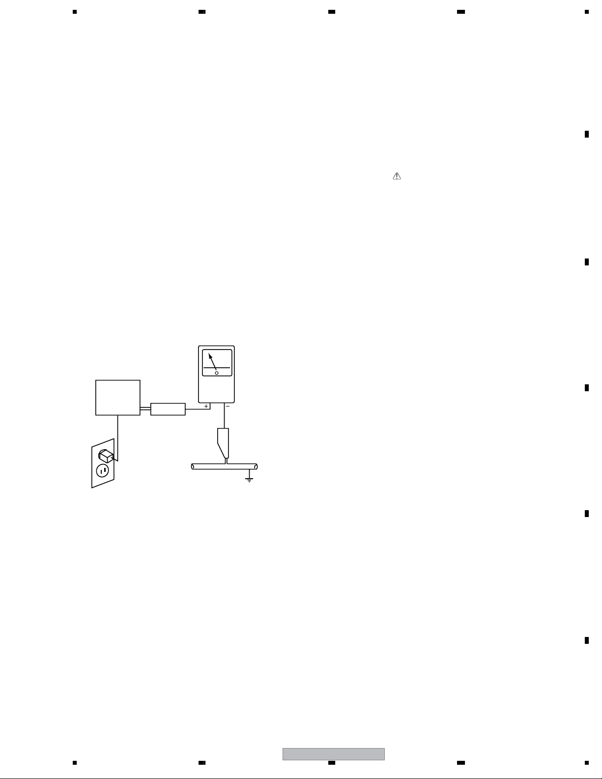
Leakage Current Cold Check
With the AC plug removed from an AC power source, place a
jumper across the two plug prongs. Turn the AC power switch on.
Using an insulation tester (DC 500V), connect one lead to the
jumpered AC plug and touch the other lead to each exposed metal
part (input/output terminals, screwheads, metal overlays, control
shafts, etc.), particularly any exposed metal part having a return
path to the chassis. Exposed metal parts having a return path to
the chassis should have a minimum resistor reading of 4MΩ. The
below 4MΩ resistor value indicate an abnormality which require
corrective action. Exposed metal parts not having a return path to
the chassis will indicate an open circuit.
Leakage Current Hot Check
Plug the AC line cord directly into an AC power source (do not
use an isolation transformer for this check).
Turn the AC power switch on.
Using a "Leakage Current Tester (Simpson Model 229
equivalent)", measure for current from all exposed metal parts of
the cabinet (input/output terminals, screwheads, metal overlays,
control shaft, etc.), particularly any exposed metal part having a
return path to the chassis, to a known earth ground (water pipe,
conduit, etc.). Any current measured must not exceed 1mA.
PRODUCT SAFETY NOTICE
Many electrical and mechanical parts in PIONEER set have
special safety related characteristics. These are often not evident
from visual inspection nor the protection afforded by them
necessarily can be obtained by using replacement components
rated for higher voltage, wattage, etc. Replacement parts which
have these special safety characteristics are identified in this
Service Manual.
Electrical components having such features are identified by
marking with a on the schematics and on the parts list in this
Service Manual.
The use of a substitute replacement component which dose not
have the same safety characteristics as the PIONEER
recommended replacement one, shown in the parts list in this
Service Manual, may create shock, fire or other hazards.
Product Safety is continuously under review and new instructions
are issued from time to time. For the latest information, always
consult the current PIONEER Service Manual. A subscription to,
or additional copies of, PIONEER Service Manual may be
obtained at a nominal charge from PIONEER.
A
B
C
Reading should
not be above
1mA
Earth
ground
Device
under
test
Also test with
plug reversed
(Using AC adapter
plug as required)
Leakage
current
tester
Test all
exposed metal
surfaces
AC Leakage Test
ANY MEASUREMENTS NOT WITHIN THE LIMITS
OUTLINED ABOVE ARE INDICATIVE OF A POTENTIAL
SHOCK HAZARD AND MUST BE CORRECTED BEFORE
RETURNING THE SET TO THE CUSTOMER.
D
E
56
PDP-5071PU
F
3
7
8
1234
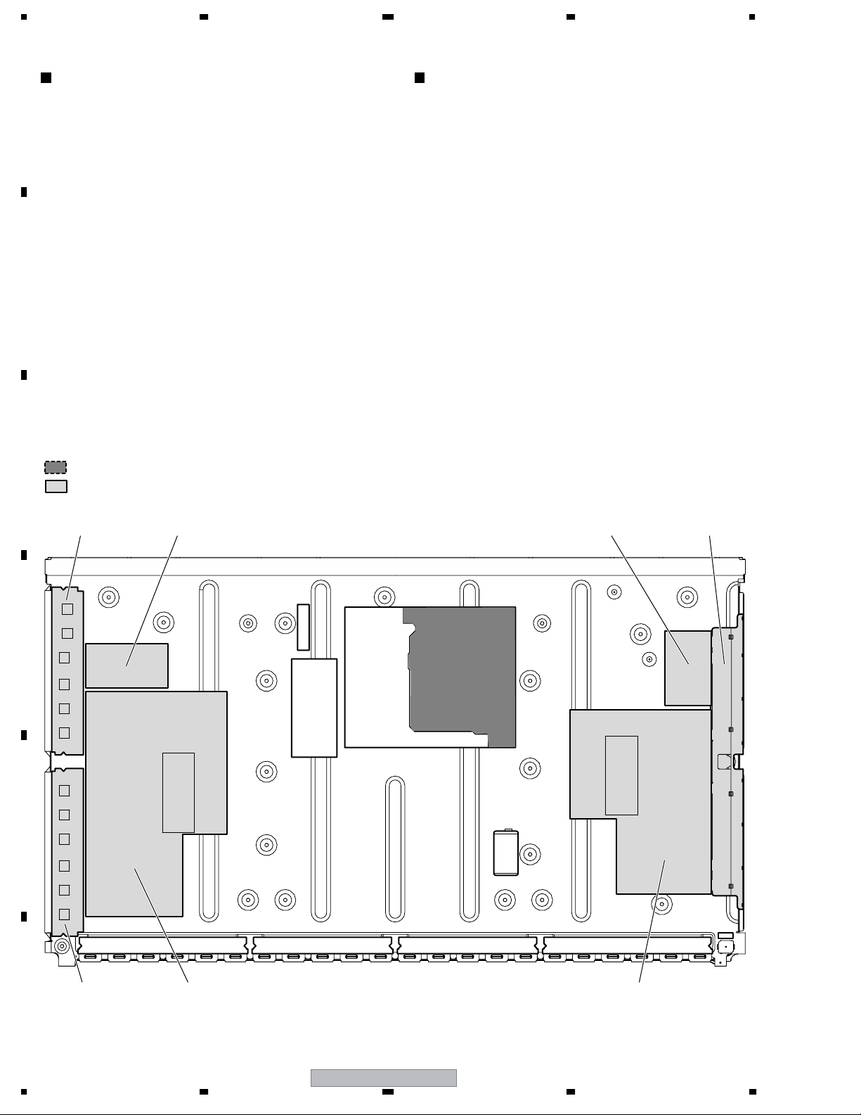
Charged Section
The places where the commercial AC power is used without
A
passing through the power supply transformer.
If the places are touched, there is a risk of electric shock. In
addition, the measuring equipment can be damaged if it is
connected to the GND of the charged section and the GND of the
non-charged section while connecting the set directly to the
commercial AC power supply. Therefore, be sure to connect the
set via an insulated transformer and supply the current.
1. Power Cord
2. AC Inlet
3. Power Switch (S1)
B
4. Fuse (In the POWER SUPPLY Unit)
5. STB Transformer and Converter Transformer
(In the POWER SUPPLY Unit)
6. Other primary side of the POWER SUPPLY Unit
C
: Part is Charged Section.
: Part is the High Voltage Generating Points
other than the Charged Section.
High Voltage Generating Point
The places where voltage is 100 V or more except for the charged
places described above. If the places are touched, there is a risk of
electric shock.
The VSUS voltage remains for several minutes after the power to
the unit is turned off. These places must not be touched until
about 10 minutes after the power is turned off, or it is confirmed
with a tester that there is no residual VSUS voltage.
If the procedures described in “10.3 POWER ON/OFF FUNC-
-TION FOR THE LARGE-SIGNAL SYSTEM” are performed
before the power is turned off, the voltage will be discharged in
about 30 seconds.
POWER SUPPLY UNIT ....................................................(205 V)
50 X MAIN DRIVE Assy...................................(–180 V to 205 V)
50 X SUB DRIVE Assy......................................(–180 V to 205 V)
50 Y MAIN DRIVE Assy....................................................(500 V)
50 Y SUB DRIVE Assy.......................................................(350 V)
50 SCAN A Assy..................................................................(500 V)
50 SCAN B Assy..................................................................(500 V)
50 SCAN B Assy 50 Y SUB DRIVE Assy 50 X SUB DRIVE Assy Conductive plate X
D
E
50 SCAN A Assy 50 Y MAIN DRIVE Assy 50 X MAIN DRIVE Assy
F
Fig.1 High Voltage Generating Point (Rear view)
4
1234
PDP-5071PU
5678
[Important Check Points for Good Servicing]
In this manual, procedures that must be performed during repairs are marked with the below symbol.
Please be sure to confirm and follow these procedures.
1. Product safety
Please conform to product regulations (such as safety and radiation regulations), and maintain a safe servicing environment by
following the safety instructions described in this manual.
1 Use specified parts for repair.
Use genuine parts. Be sure to use important parts for safety.
2 Do not perform modifications without proper instructions.
Please follow the specified safety methods when modification(addition/change of parts) is required due to interferences such as
radio/TV interference and foreign noise.
3 Make sure the soldering of repaired locations is properly performed.
When you solder while repairing, please be sure that there are no cold solder and other debris.
Soldering should be finished with the proper quantity. (Refer to the example)
4 Make sure the screws are tightly fastened.
Please be sure that all screws are fastened, and that there are no loose screws.
5 Make sure each connectors are correctly inserted.
Please be sure that all connectors are inserted, and that there are no imperfect insertion.
6 Make sure the wiring cables are set to their original state.
Please replace the wiring and cables to the original state after repairs.
In addition, be sure that there are no pinched wires, etc.
7 Make sure screws and soldering scraps do not remain inside the product.
Please check that neither solder debris nor screws remain inside the product.
8 There should be no semi-broken wires, scratches, melting, etc. on the coating of the power cord.
Damaged power cords may lead to fire accidents, so please be sure that there are no damages.
If you find a damaged power cord, please exchange it with a suitable one.
9 There should be no spark traces or similar marks on the power plug.
When spark traces or similar marks are found on the power supply plug, please check the connection and advise on secure
connections and suitable usage. Please exchange the power cord if necessary.
0 Safe environment should be secured during servicing.
When you perform repairs, please pay attention to static electricity, furniture, household articles, etc. in order to prevent injuries.
Please pay attention to your surroundings and repair safely.
A
B
C
D
2. Adjustments
To keep the original performance of the products, optimum adjustments and confirmation of characteristics within specification.
Adjustments should be performed in accordance with the procedures/instructions described in this manual.
3. Lubricants, Glues, and Replacement parts
Use grease and adhesives that are equal to the specified substance.
Make sure the proper amount is applied.
4. Cleaning
For parts that require cleaning, such as optical pickups, tape deck heads, lenses and mirrors used in projection monitors, proper
cleaning should be performed to restore their performances.
5. Shipping mode and Shipping screws
To protect products from damages or failures during transit, the shipping mode should be set or the shipping screws should be
installed before shipment. Please be sure to follow this method especially if it is specified in this manual.
56
PDP-5071PU
E
F
5
7
8
1234
1.2 QUICK REFERENCE UPON SERVICE VISIT
A
Notes, PD/SD diagnosis, and methods for various settings
Notes when visiting for service
1. Notes when disassembling/reassembling
1 Rear case
When reassembling the rear case, the screws must be tightened in a
specific order. Be careful not to tighten them in the wrong order forcibly.
For details, see "Rear Case" in "6. DISASSEMBLY"
2 Attaching screws for the HDMI connector
When attaching the HDMI connector after replacing the Main Assy,
secure the HDMI connector manually with a screwdriver, but not
with an electric screwdriver. If you tighten the screws too tightly
with an electric screwdriver, the screw heads may be damaged, in
B
C
which case the screws cannot be untightened/tightened any more.
2. On parts replacement
1 How to discharge before replacing the Assys
A charge of significant voltage remains in the Plasma Panel even
after the power is turned off. Safely discharge the panel before
replacement of parts, in either manner indicated below:
Let the panel sit at least for 3 minutes after the power is turned off.
A:
B: Turn the Large Signal System off before the power is turned off
then, after 1 minute, turn the power off.
For details, see "10.2 Power ON/OFF Function for the Large-Signal
System."
2 On the settings after replacement of the Assys
Some boards need settings made after replacement of the Assys.
For details, see "7. ADJUSTMENT"
3. On various settings
1 SR+
After a repair using a PC, be sure to restore the setting for the
RS-232C connector to SR+.
2 Setting in Factory mode
After a Mask indication into the panel is performed, be sure to
set the Mask setting to "OFF" then exit Factory mode.
Quick Reference upon Service Visit 1
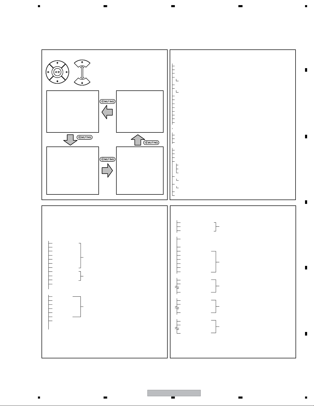
PD/SD
Item
Communication with the panel drive IC
Communication with the module IIC
DIGTAL-RST2
Panel high temperature
Panel section
Audio
Communication with the Module microcomputer
Main 3-wire serial communication
Main IIC communication
Communication with the Main microcomputer
FAN
Main section
Unit high temperature
Communication with the D-TUNER
MTB-RST2/RST4
POWER
SCAN
SCN-5V
Y-DRIVE
Y-DCDC
Y-SUS
ADRS
X-DRIVE
X-DCDC
X-SUS
UNKNOWN
No. of LEDs
flashing
Red Blue
Blue 1
Blue 2
Blue 3
Blue 4
Blue 5
Blue 6
Blue 7
Blue 8
Blue 9
Blue 10
Blue 11
Blue 12
Blue 13
Red 2
Red 3
Red 4
Red 5
Red 6
Red 7
Red 8
Red 9
Red 10
Red 11
Red 15
Change of settings
How to enter Factory mode using
the supplied remote control unit
In the same way as with the remote
control unit supplied with the 6thgeneration model
How to enter Integrator mode using
the supplied remote control unit
1 Enter the Standby mode.
2 Press [MENU].
3 Press [TV ].
Release TRAP SW-ERR
1 Enter the Factory mode.
2 Select the INITIALIZE mode.
3 Hold [DISPLAY] pressed for at least
5 seconds.
How to switch UART 1 (Integrator)
1 Enter the Integrator mode.
2 Display "OFF" using [\].
3 Change the communication speed
using [«], then [\].
How to switch UART 2 (During Standby)
1 Enter the Standby mode.
2
Hold [VOL +] or [VOL -] pressed for 3 seconds.
3
Hold [SPLIT] pressed for 3 seconds.
4-1 To set to 232C, press [ENTER].
5-2
To set to SR+, press [HOME MENU].
Note:
If switching is completed successfully,
the red LED will flash twice.
Note 1:
Use a remote control unit supplied with
the 6th-generation models or later.
Note 2:
Do not hold a key pressed for more
than 5 seconds.
How to locate several items on the Factory menu
{ } : Item on the Factory menu
D
E
F
[ ] : Key on the remote control unit
" " : Screen indication
1. Confirmation of accumulated power-on time and power-on
count
Select {INFORMATION} then {HOUR METER}.
(After entering Factory mode, press [«] four times.)
2. Confirmation of the Power-down and Shutdown histories
1 Panel system
PD: Select {PANEL FACTORY} then {POWER DOWN}.
(After entering Factory mode, press [MUTING] once, press
[ENTER], then press [«] three times.)
SD: Select {PANEL FACTORY} then {SHUT DOWN}.
(After entering Factory mode, press [MUTING] once, press
[ENTER], then press [«] four times.)
2 Main Assy
Select {INFORMATION} then {MAIN NG}.
(After entering Factory mode, press [«] three times.)
3. How to display the Mask indication
1 Mask indication in the panel side
1. Select {PANEL FACTORY} then {RASTER MASK SETUP}.
(After entering Factory mode, press [MUTING] once, press [ENTER],
then press [«] 8 times.)
2. Press [ENTER], then select a Mask indication, using [»] or [«].
2 Mask (SG screen) indication in the Main Assy (MAIN VDEC)
1. Select either Input 1 or 2 or 4, to which no signal is input (
2. Select {INITIALIZE} then {SG MODE}. Press [|]. (After entering
Factory mode, press [MUTING] three times, then press [«] once.)
Then, the indication at the lower right of the screen changes from
"OFF" to "ANA AD YCBCR".
3. You can change Mask patterns by pressing [«] to select {SG
PATTERN} then using [|] or [\].
Note: When you switch "SG MODE" routes, some displays become
monochrome, as they are in Y-signal only mode.
black screen
Adjustments and Settings after replacement of the
Assys (Procedures in Factory mode)
1. Digital Video Assy: Transfer of backup data
1 Select {PANEL FACTORY}, {ETC}, then {BACKUP DATA}. (After entering Factory
mode, press [MUTING] once, press [ENTER], press [«] seven times, then press
[ENTER].)
2 Select {TRANSFER}, using [\], then hold [SET] pressed for at least 5 seconds.
3 After transfer of backup data is completed, {ETC} is automatically selected, and the
LED on the front panel returns to normal lighting.
2. MAIN Assy (U): Execution of FINAL SETUP.
1 Select {INITIALIZE} then {FINAL SETUP}, then press [ENTER]. (After entering
Factory mode, press [MUTING] three times, then press [«] four times.)
2 Select "YES", using [\]. Then hold [ENTER] pressed for at least 5 seconds.
3 After "FINAL SETUP IS COMPLETE" is displayed on the screen, turn the POWER
switch of the main unit off.
3. POWER SUPPLY Unit: Clearance of the accumulated power-on count
and maximum temperature value
1 Select {PANEL FACTORY}, {ETC}, then {P COUNT INFO}. (After entering Factory
mode, press [MUTING] once, press [ENTER], press [«] seven times, press [ENTER],
then press [«] six times.)
2 Press [\] to select "CLEAR". Hold [SET] pressed for at least 5 seconds.
After clearance is completed, "ETC" is automatically selected. Clear the maximum
temperature value (MAX TEMP) in the same manner.
4. Other Assys: Clearance of the maximum temperature value
1 Select {PANEL FACTORY}, {ETC}, then {MAX TEMP}. (After entering Factory mode,
press [MUTING] once, press [ENTER], press [«] seven times, press [ENTER], then
press [«] seven times.)
2 Press [\] to select "CLEAR". Hold [SET] pressed for at least 5 seconds.
After clearance is completed, "ETC" is automatically selected.
).
6
PDP-5071PU
1234
5678
Quick Reference upon Service Visit 2
Mode transition and structure of layers in Service Factory mode
Mode transition in Service Factory mode
INFORMATION mode
1. VERSION (1)
2. VERSION (2), (3)
3. MAIN NG
4. TEMPERATURE
5. HOUR METER
6. HDMI SIGNAL INFO1, 2
7. VDEC SIGNAL INFO 2
8. DTV TUNING STATUS 1, 2, 3
9. DTV TV-GUIDE BER
10. DEBUG INFO
PANEL FACTORY mode
1. PANEL INFORMATION
2. PANEL WORKS
3. POWER DOWN
4. SHUT DOWN
5. PANEL-1 ADJ
6. PANEL-2 ADJ
7. PANEL REVICE
8. ETC.
9. RASTER MASK SETUP
10. PATTEN MASK SETUP
11. COMBI MASK SETUP
Up
Down
• To shift to another mode, press [MUTING].
• To shift to another item in a specific mode,
press [»] or [«].
• To shift to the next nested layer below for an
item with a "(+)" indication, press [ENTER].
To return to the next nested layer above,
also press [ENTER].
INITIALIZE mode
1. SYNC DET
2. SG MODE
3. SG PATTERN
4. SIDE MASK LEVEL
5. FINAL SETUP
6. HMG/HG SERVICE MODE
7. CVT AUTO
8. HDMI INTR POSITION
OPTION mode
1. EDID WRITE MODE
2. ANTENNA MODE
3. AFT
Structure of Layers in Service Factory Mode
INFORMATION mode
1. VERSION (1) Flash Versions for PANEL system and MAIN system
2. VERSION (2) Flash Versions for DTV system
3. VERSION (3) Flash Versions for CCD ucom and HM
4. MAIN NG SD histories for MAIN (Going Clear model by SET key)
4-1. CLEAR Select Yes by [\] key \ pushing and hold [SET] key
5. TEMPERATURE TEMP 1, TEMP2 and FAN mode are displayed
6. HOUR METER Hour meter and number of Power ON are displayed
6-1. CLEAR Select Yes by [\] key \ pushing and hold [SET] key
7. HDMI SIGNAL INFO 1 For factory use
8. HDMI SIGNAL INFO 2 Signal info of HDMI are displayed ( Detail are on SM )
9. VDEC SIGNAL INFO For factory use
10. DTV TUNING STATUS 1 Detail information for DTV is displayed
11. DTV TUNING STATUS 2 Detail information for DTV is displayed
12. DTV TUNING STATUS 3 Detail information for DTV is displayed
13. DTV TV-GUIDE BER For production line use
14. DEBUG INFO For factory use
PANEL FACTORY mode Refer to [PANEL FACTORY MODE]
OPTION
1. EDID WRITE MODE For factory use
2. ANTENNA MODE For production line use
3. AFT For production line use
INITIALIZE
1. SYNC DET (+) For factory use
2. SG MODE SG signal from MAIN VDEC (
3. SG PATTERN For factory use
4. SIDE MASK LEVEL(+) For factory use
4-1. R MASK LEVEL
4-2. G MASK LEVEL
4-3. B MASK LEVEL
5. FINAL SETUP Set to Factory default settings (it should perform after
5-1. DATA RESET replacing a MAIN board )
6. HMG/HG SERVICE MODE Information for a USB device is displayed
6-1. MODE SIFT
7. CVT AUTO For factory use
8. HDMI INTR POSITION(+) For factory use
Composite signal is required
A
B
)
C
Structure of Layers in Panel Factory Mode 1
1. PANEL INFORMATION Version indication of the panel
2. PANEL WORKS Indications of the accumulated power-on time, pulse-meter
3. POWER DOWN Indication of the Power-down history
4. SHUT DOWN Indication of the Shutdown history
5. PANEL-1 ADJ (+)
1. X-SUS B
2. Y-SUS B
3. Y-SUSTAIL T1
4. Y-SUSTAIL T2 Modification not required because these items are basically
5. Y-SUSTAIL W for factory presetting
6. XY-RST W1
7. XY-RST W2
8. VOL SUS
9. VOL OFFSET Settings required after replacement of the panel
10. VOL RST P
11. SUS FREQ. For AM noise prevention (Depending on the mode,
6. PANEL-2 ADJ (+)
1. R-HIGH
2. G-HIGH
3 .B-HIGH Parameters for the WB adjustment of the panel, which are
4. R-LOW required during adjustment after panel replacement
5. G-LOW
6. B-LOW
7. ABL Setting of the power consumption. A setting table is
To "Structure of Layers in Panel Factory Mode 2"
count, and power-on count of the panel
brightness of the screen changes.)
available for each vertical signal.
Structure of Layers in Panel Factory Mode 2
7. PANEL REVISE (+)
R-LEVEL
G-LEVEL Items for use by engineers
B-LEVEL
8. ETC (+)
1. BACKUP DATA For transferring backup data (after replacement of
2. DIGITAL EEPROM To clear data of the digital video
3. PD INFO.
4. SD INFO. For clearance of data for the corresponding items.
5. HR-MTR INFO. The clearing method is the same: Select "CLEAR",
6. PM/B1-B5 using [\], then hold [SET] pressed for at least 5
7. P COUNT INFO. seconds. After clearance is completed, {ETC} is
8. MAX TEMP. automatically selected.
9. RASTER MASK SETUP (+)
1. MASK OFF
2. RST MASK 01 For use while Raster Mask (full mask) is displayed.
• • • • • Use [»] or [«] to select the type of mask.
25. RST MASK 24
10. PATTEN MASK SETUP (+)
1. MASK OFF
2. PTN MASK 01 For use while Pattern Mask is displayed. Use [»] or
• • • • • [«] to select the type of mask.
40. PTN MASK 39
11. COMBI MASK SETUP (+)
1. MASK OFF
2. CMB MASK 01 For use while Combination Mask is displayed.
• • • • • Use [»] or [«] to select the type of mask.
11. CMB MASK 10
the DIGITAL Assy)
D
E
56
PDP-5071PU
F
7
7
8

1234
1.3 JIGS LIST
A
Cleaning
Name Part No. Remarks
Cleaning liquid GEM1004
Cleaning paper GED-008
B
Used to fan cleaning.
Refer to "2.4 CHASSIS SECTION (1/2).
CONTENTS
1. NOTES ON SERVICE VISIT............................................................................................................................. 2
1.1 SAFETY INFORMATION ........................................................................................................................... 2
1.2 QUICK REFERENCE UPON SERVICE VISIT........................................................................................... 6
1.3 JIGS LIST .................................................................................................................................................. 8
2. EXPLODED VIEWS AND PARTS LIST .......................................................................................................... 10
2.1 PACKING SECTION ................................................................................................................................ 10
2.2 REAR SECTION ...................................................................................................................................... 12
C
D
E
F
2.3 FRONT SECTION.................................................................................................................................... 14
2.4 CHASSIS SECTION (1/2)........................................................................................................................ 16
2.5 CHASSIS SECTION (2/2)........................................................................................................................ 18
2.6 PANEL CHASSIS SECTION.................................................................................................................... 20
2.7 MULTIBASE SECTION ............................................................................................................................ 22
2.8 PDP SERVICE ASSY 507 (AWU1212).................................................................................................... 24
2.9 TABLE TOP STAND ................................................................................................................................. 26
3. PCB PARTS LIST ........................................................................................................................................... 27
4. BLOCK DIAGRAM AND SCHEMATIC DIAGRAM..........................................................................................44
4.1 OVERALL CONNECTION DIAGRAM (1/2) ............................................................................................. 44
4.2 OVERALL CONNECTION DIAGRAM (2/2) ............................................................................................. 46
4.3 OVERALL BLOCK DIAGRAM (1/2) ......................................................................................................... 48
4.4 OVERALL BLOCK DIAGRAM (2/2) ......................................................................................................... 50
4.5 50 ADDRESS S and L ASSYS ................................................................................................................ 51
4.6 50 SCAN A and B ASSYS ....................................................................................................................... 52
4.7 50X MAIN DRIVE and 50X SUB DRIVE ASSYS..................................................................................... 53
4.8 50Y MAIN DRIVE and 50Y SUB DRIVE ASSYS..................................................................................... 54
4.9 50 DIGITAL ASSY.................................................................................................................................... 55
4.10 AUDIO ASSY ......................................................................................................................................... 56
4.11 SIGNAL BLOCK DIAGRAM................................................................................................................... 58
4.12 DTV BLOCK DIAGRAM......................................................................................................................... 60
4.13 50 X/Y DRIVE POWER LINE BLOCK DIAGRAM.................................................................................. 62
4.14 FUKUGO BLOCK POWER LINE BLOCK DIAGRAM............................................................................ 63
4.15 POWER SUPPLY UNIT.......................................................................................................................... 64
4.16 VOLTAGES............................................................................................................................................. 65
4.17 WAVEFORMS ........................................................................................................................................ 78
5. DIAGNOSIS INFORMATION .......................................................................................................................... 82
5.1 THE FLOW OF DIAGNOSIS.................................................................................................................... 82
5.1.1 FLOWCHART OF FAILURE ANALYSIS FOR THE WHOLE UNIT .................................................... 82
5.1.2 FLOWCHART OF FAILURE ANALYSIS FOR THE POWER SUPPLY UNIT..................................... 84
5.1.3 FLOWCHART OF FAILURE ANALYSIS FOR THE DIGITAL ASSY .................................................. 85
5.1.4 FLOWCHART OF FAILURE ANALYSIS FOR THE DRIVE ASSY..................................................... 86
5.1.5 FLOWCHART OF FAILURE ANALYSIS FOR THE MAIN ASSY....................................................... 90
5.1.6 FLOWCHART OF FAILURE ANALYSIS FOR THE VIDEO SYSTEM................................................ 91
5.1.7 FLOWCHART OF FAILURE ANALYSIS FOR THE AUDIO SYSTEM ............................................... 97
5.2 POWER DOWN ..................................................................................................................................... 101
5.2.1 BLOCK DIAGRAM OF THE POWER-DOWN SIGNAL.................................................................... 101
5.2.2 POWER DOWN OF FAILURE ANALYSIS ....................................................................................... 102
5.3 SHUT DOWN......................................................................................................................................... 104
8
1234
PDP-5071PU

5678
5.3.1 BLOCK DIAGRAM OF THE SHUT-DOWN SIGNAL ........................................................................104
5.3.2 SHUT DOWN OF FAILURE ANALYSIS ...........................................................................................105
5.4 NON-FAILURE SYMPTOMS ..................................................................................................................106
6. DISASSEMBLY .............................................................................................................................................107
6.1 PCB LOCATION .....................................................................................................................................107
6.2 FLOWCHART OF THE MAIN PARTS AND PC BOARDS EXCHANGE.................................................108
7. ADJUSTMENT ..............................................................................................................................................113
7.1 PARTS CHANGE OF NOTES.................................................................................................................113
7.2 ADJUSTMENT REQUIRED WHEN THE SET IS REPAIRED OR REPLACED......................................113
7.3 ADJUSTMENT REQUIRED WHEN PART IS REPLACED.....................................................................114
7.4 BACKUP WHEN THE PANEL UNIT IS ADJUSTED ...............................................................................115
7.5 EXCHANGE OF SERVICE PANEL ASSY ..............................................................................................118
7.5.1 ADJUSTMENTS WHEN THE SERVICE PANEL ASSY IS REPLACED...........................................118
7.6 ADJUSTMENTS WHEN THE DRIVE ASSYS ARE REPLACED............................................................125
7.7 HOW TO CLEAR HISTORY DATA ..........................................................................................................128
7.8 PROCEDURE WHEN REPLACING THE POWER SUPPLY UNIT.........................................................129
8. SERVICE FACTORY MODE .........................................................................................................................130
8.1 SERVICE FACTORY MODE OUTLINE ..................................................................................................130
8.1.1 TRANSITION DIAGRAM OF SERVICE FACTORY MODE..............................................................130
8.1.2 HOW TO ENTER/EXIT SERVICE FACTORY MODE.......................................................................130
8.1.3 OPERATION OF SERVICE FACTORY MODE.................................................................................131
8.1.4 REMOTE CONTROL CODE ............................................................................................................132
8.1.5 CONFIGURATION OF FACTORY MODE ........................................................................................133
8.1.6 INDICATION (OSD) OF SERVICE FACTORY MODE......................................................................134
8.2 FACTORY MENU....................................................................................................................................136
8.2.1 INFORMATION.................................................................................................................................136
8.2.2 PANEL FACTORY MODE.................................................................................................................145
8.2.3 OPTION MODE................................................................................................................................155
8.2.4 INITIALIZE MODE............................................................................................................................156
9. LIST OF RS-232C COMMANDS ..................................................................................................................161
9.1 RS-232C COMMANDS OUTLINE ..........................................................................................................161
9.1.1 PREPARED TOOLS .........................................................................................................................161
9.1.2 USING RS-232C COMMANDS........................................................................................................161
9.1.3 COMMAND PROTOCOL..................................................................................................................162
9.1.4 DEFINITION OF COMMAND ...........................................................................................................163
9.2 LIST OF RS-232C COMMANDS ............................................................................................................164
9.3 OUTLINE OF COMMANDS....................................................................................................................170
9.3.1 QS1 ..................................................................................................................................................170
9.3.2 QS2 ..................................................................................................................................................171
9.3.3 QIP ...................................................................................................................................................172
9.3.4 QAJ ..................................................................................................................................................172
9.3.5 QPW.................................................................................................................................................173
9.3.6 QPM .................................................................................................................................................173
9.3.7 QPD..................................................................................................................................................174
9.3.8 QSD..................................................................................................................................................175
9.3.9 QS6 ..................................................................................................................................................176
9.3.10 QSI .................................................................................................................................................177
9.3.11 QMT ...............................................................................................................................................178
9.3.12 QNG ...............................................................................................................................................178
9.3.13 DRV................................................................................................................................................179
9.3.14 COMMANDS FOR PROHIBITION/PERMISSION OF DTV/HOMENET COMMUNICATION ........180
9.3.15 OTHER COMMANDS ....................................................................................................................181
10. GENERAL INFORMATION .........................................................................................................................182
10.1 POWER ON SEQUENCE.....................................................................................................................182
10.2 POWER SUPPLY TRANSITION STATUS.............................................................................................183
10.3 POWER ON/OFF FUNCTION FOR THE LARGE-SIGNAL SYSTEM ..................................................186
10.4 LED INFORMATION.............................................................................................................................187
10.5 SPECIFICATION ABOUT THE THERMAL PROTECTION...................................................................188
10.6 PROCESSING IN ABNORMALITY ......................................................................................................189
10.7 TRAP SW..............................................................................................................................................190
11. SPECIFICATIONS .......................................................................................................................................191
11.1 MAIN SPECIFICATIONS ......................................................................................................................191
11.2 ACCESSORIES....................................................................................................................................192
11.3 PANEL FACILITIES...............................................................................................................................193
12. IC INFORMATION .......................................................................................................................................196
A
B
C
D
E
F
56
PDP-5071PU
9
7
8
1234
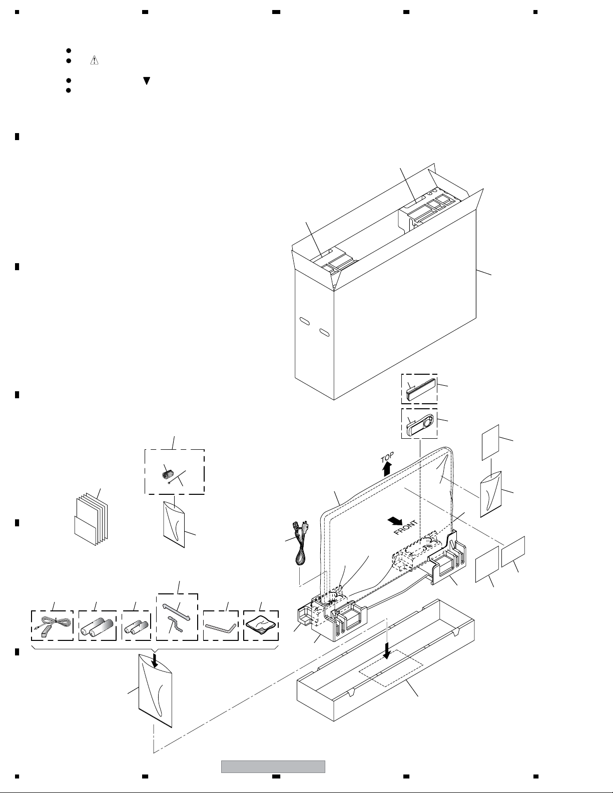
2. EXPLODED VIEWS AND PARTS LIST
NOTES:
Parts marked by "NSP" are generally unavailable because they are not in our Master Spare Parts List.
The mark found on some component parts indicates the importance of the safety factor of the part.
A
Therefore, when replacing, be sure to use parts of identical designation.
Screws adjacent to mark on product are used for disassembly.
For the applying amount of lubricants or glue, follow the instructions in this manual.
(In the case of no amount instructions, apply as you think it appropriate.)
2.1 PACKING SECTION
B
C
22
21
27
4
6
9
Noise filter
D
13, 15, 18
E
2 11 12
7
for antenna cable
Binder for noise filter
8
10
Speed clamp ×3
Bead band ×3
29
28
1
25
23
3
5
17
20
25
14
24
16
19
F
10
1234
PDP-5071PU
26
>
5678
(1) PACKING PARTS LIST
No. Description Part No.
Mark
1Power Cord (2 m) ADG1215
2 G-LINK Cable (3 m) VDX1010
3 Remote Control Unit AXD1536
4 Battery Cover AZN2680
5 Simpled Remote Control Unit See Contrast table (2)
6 Battery Cover See Contrast table (2)
NSP 7
NSP 8 Dry Cell Battery (R03, AAA) See Contrast table (2)
9 Filter CTX1054
10 Binder Assy AEC1908
NSP 11 Hexagonal Wrench (6 mm) AEF1029
12 Cleaning Cloth AED1285
13 Operating Instructions ARE1426
(English, French, Spanish)
14 Caution Card ARM1239
15 Cleaning Caution (U) ARM1303
Alkaline Dry Cell Battery (LR6, AA)
VEM1023
No. Description Part No.
Mark
16 Accessory Caution ARM1304
NSP 17 Warranty Card ARY1196
NSP 18 Card (Register) ARY1156
19 Polyethlene Bag AHG1394
20 Vinyl Bag AHG1347
21 Pad (507REG. T-L) AHA2571
22 Pad (507REG. T-R) AHA2572
23 Pad (507REG. B-L) AHA2573
24 Pad (507REG. B-R) AHA2574
25 Pad (507EL. B-ACC.) AHA2575
26 Under Carton (507REG) AHD3484
27 Upper Carton (507REG) See Contrast table (2)
28 Packing Sheet L AHG1389
29 Polyethylene Bag S AHG1395
A
B
(2) CONTRAST TABLE
PDP-5071PU/KUCXC and PDP-5070PU/KUCXC are constructed the same except for the following:
Mark No. Symbol and Description
5 Simpled Remote Control Unit AXD1539 Not used
6 Battery Cover AZN2682 Not used
NSP 8 Dry Cell Battery (R03, AAA) VEM1036 Not used
27 Upper Carton AHD3485 AHD3523
PDP-5071PU
/KUCXC
PDP-5070PU
/KUCXC
C
D
E
56
PDP-5071PU
F
11
7
8
1234
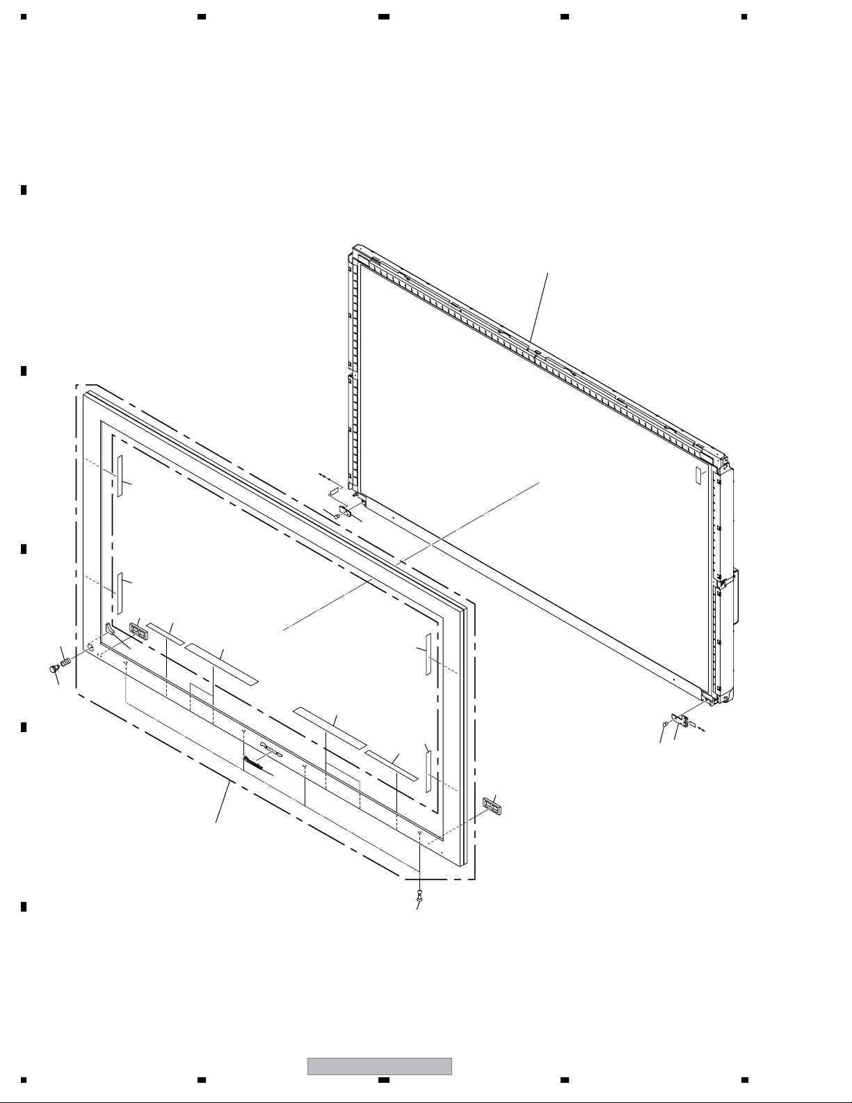
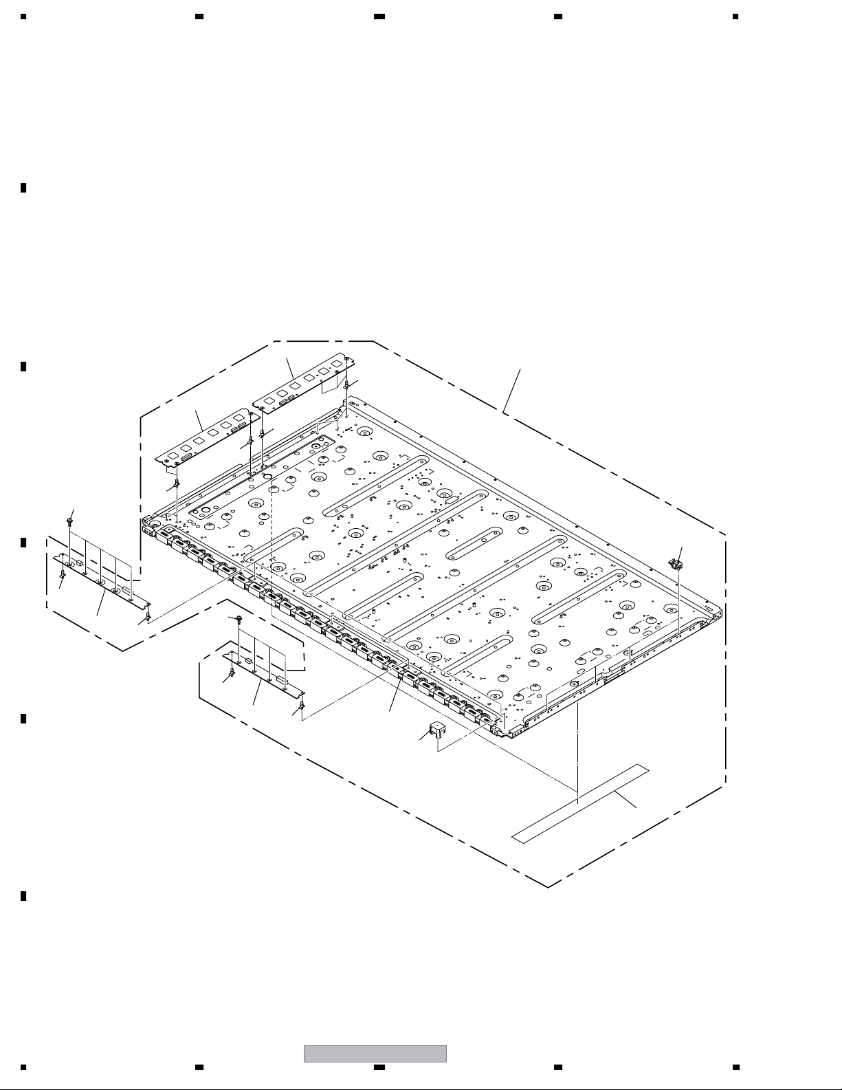
2.2 REAR SECTION
A
36
15 18
33
40
36
36
20
17
15
19
36
B
23
22
36
40
40
34
36
33
29
C
26
37
28
36
1
38
31
18
36
MAIN
CN4010
38
13
36
6
8
11
MAIN
D
USB
12
11
7
2
9
14
4
10
38
16
38
5
30
36
27
A
39
36
E
36
24
36
39
39
36
36
36
A
39
36
F
25
TANSHI
CN8801
Refer to
"2.3 FRONT SECTION".
12
1234
PDP-5071PU
5678
(1) REAR SECTION PARTS LIST
No. Description Part No.
Mark
1 SIDE KEY Assy AWW1133
2 SIDE Assy AWW1157
3• • • • •
4 USB Cable 120 cm (J301) ADF1034
5 Side Input Panel (U) ANC2392
No. Description Part No.
Mark
21 Side Spacer 507 AED1311
22 Terminal Display Label A (U/B) AAX3325
23 Terminal Display Label C (U/B) AAX3330
24
25 Terminal Panel B (50U) ANC2409
Te r minal Display Label B50 (U/B)
AAX3414
A
6 Function Button Base ANG2923
7 Side Input Shield ANK1834
8 Function Button Shield ANK1835
NSP 9 PCB Support AEC1288
10 PCB Spacer AEC1570
11 Wire Saddle AEC1745
12 Re-use Wire Saddle AEC1945
13 Locking Card Spacer AEC2019
14 USB Spacer AED1310
15 Inner Grip Assy AMR3434
16 Gasket (USB) ANK1846
NSP 17 Name Label (507PU) See Contrast table (2)
18 Side Spacer 507 AED1311
19 Bolt Caution Label AAX3075
NSP 20 Serial Seal AAX3182
26 Function Button Panel AMB2906
27 Side Input Cover AMB2911
28 Function Button AAC1562
29 Function Button Sheet (U) AAK2895
30 Input Cover Label U AAX3363
31 Rear Case (507) ANE1656
32 • • • • •
33 Screw (3 x 40P) ABA1332
34 Screw ABA1341
35 • • • • •
36 Screw AMZ30P060FTB
37 Screw AMZ30P080FTC
38 Screw APZ30P080FTB
39 Screw BPZ30P080FTB
40 Screw TBZ40P080FTB
(2) CONTRAST TABLE
PDP-5071PU/KUCXC and PDP-5070PU/KUCXC are constructed the same except for the following:
Mark No. Symbol and Description
NSP 17 Name Label AAL2766 AAL2810
PDP-5071PU
/KUCXC
PDP-5070PU
/KUCXC
B
C
D
E
F
56
PDP-5071PU
13
7
8
1234
2.3 FRONT SECTION
A
B
Refer to
"2.4 CHASSIS SECTION (1)".
C
MAIN
CN4006
10
8
1
10
7
11
D
6
4
10
10
12
10
MAIN
10
11
5
E
7
8
CN4010,
CN4006
2
3
9
F
14
1234
PDP-5071PU

5678
(1) FRONT SECTION PARTS LIST
No. Description Part No.
Mark
1 50 LED Assy AWW1135
2 LED IR Assy AWW1136
3Front Case Assy (507PU) AMB2917
4 Corner Cushion AEB1416
5 Pioneer Name Plate AAM1098
6 Coil Spring ABH1120
7 Blind Cushion AEB1415
8 Nyron Rivet AEC1671
9 Screw Rivet AEC1877
10 Insulation Sheet A AED1283
A
11 Insulation Sheet B AED1284
12 Power Button AAD4133
B
C
D
56
PDP-5071PU
E
F
15
7
8
1234
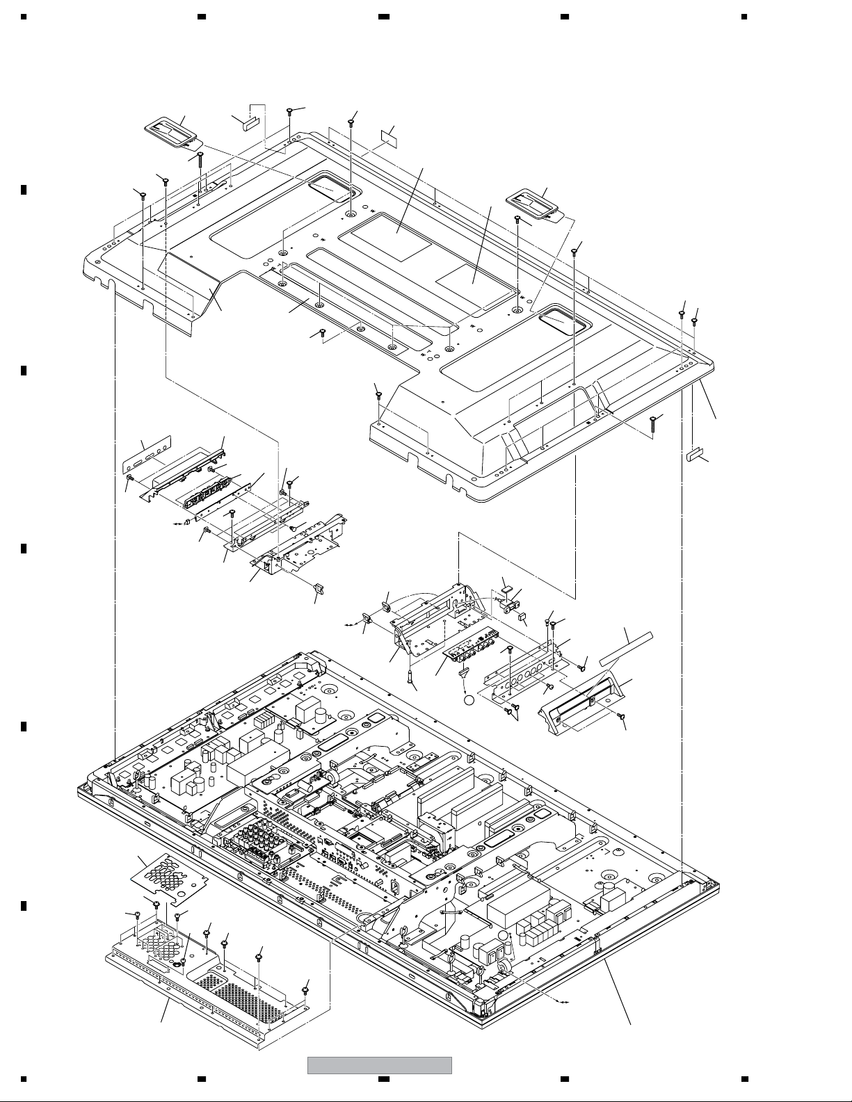
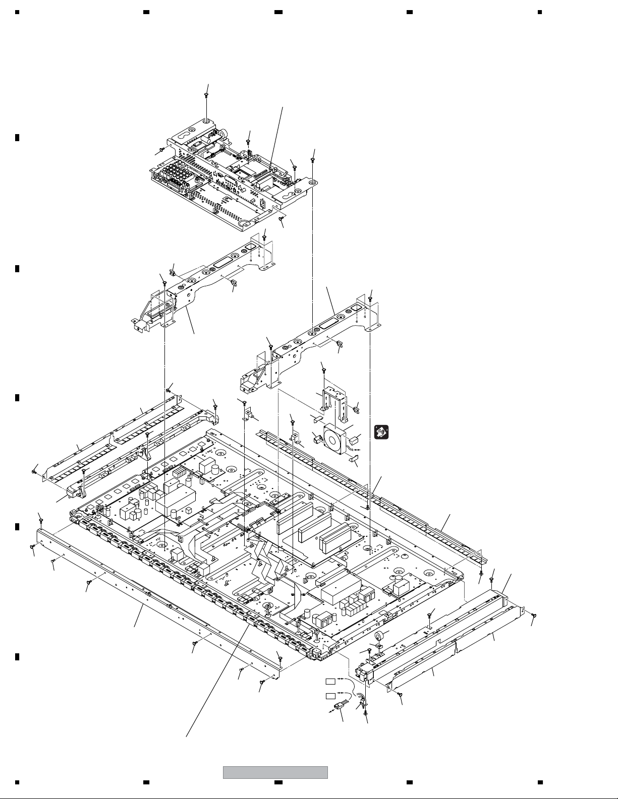
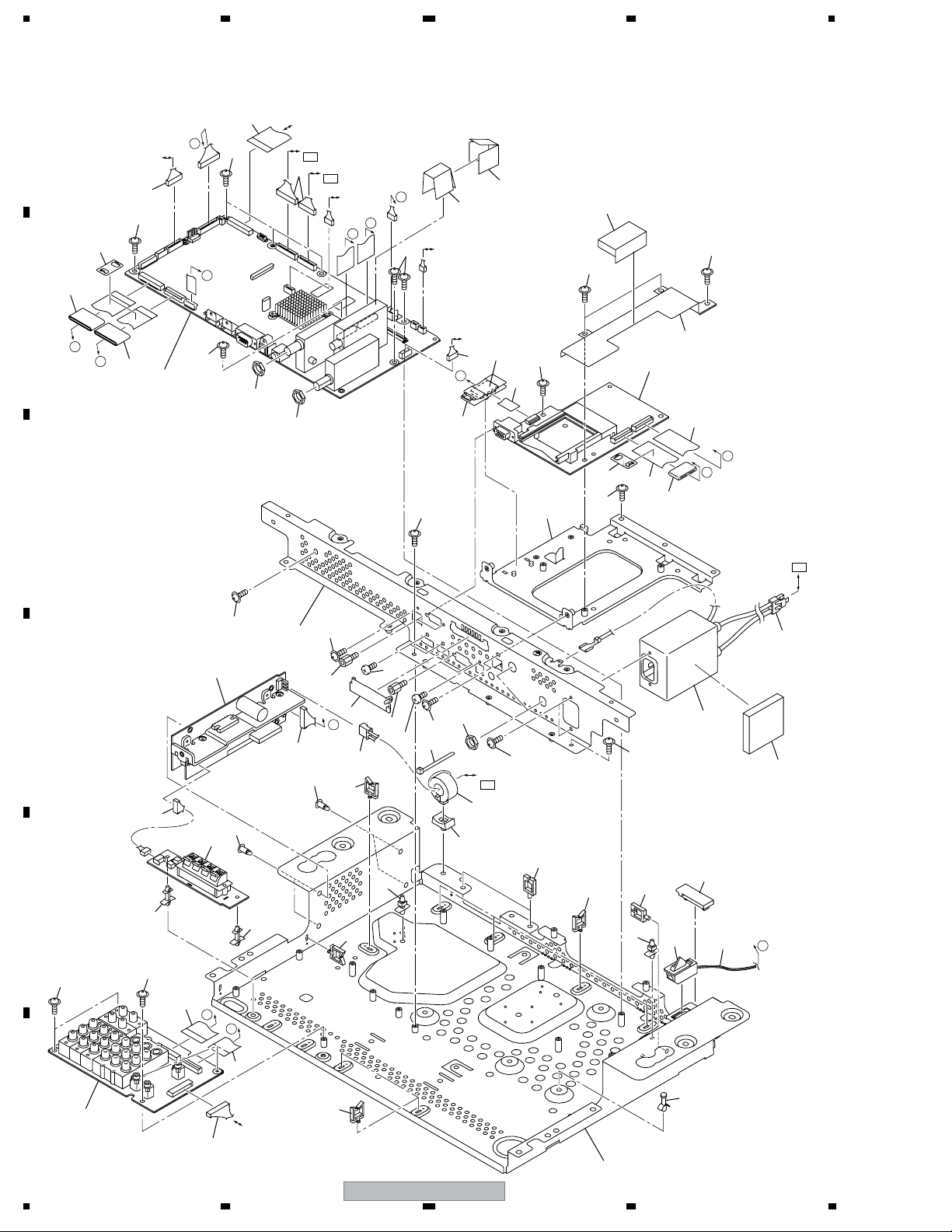
2.4 CHASSIS SECTION (1/2)
A
23
Refer to
"2.7 MULTI BASE SECTION".
28
23
27
28
23
23
B
17
27
8
27
17
C
7
27
21
17
22
22
15
15
14
13
POWER
POWER
AC inlet
P10
19
3
15
CN4009
15
25
Cleaning liquid : GEM1004
Cleaning paper : GED-008
MAIN
10
10
21
6
25
21
18
2
11
22
21
12
P3
1
4
26
22
21
12
21
22
14
11
22
D
5
24
21
22
16
E
23
9
24
23
16
22
F
Refer to
"2.5 CHASSIS SECTION (2)".
16
PDP-5071PU
1234

5678
CHASSIS SECTION (1/2) PARTS LIST
No. Description Part No.
Mark
1Power Switch (S1) ASG1092
2Ferrite Core ATX1044
3Fan Motor 80 x 25L AXM1058
4 Housing Wire (J103) ADX3352
5Front Chassis VL (50) AMA1014
6Front Chassis VR (507) AMA1022
7 Sub Frame L Assy 507 ANA1945
8 Sub Frame R Assy 507 ANA1946
9Front Chassis H Assy (507) ANA2031
10 Panel Holder H (50) ANG2769
>
A
11 Panel Holder V1 (50) ANG2770
12 Panel Holder V2 (50) ANG2771
13 Fan Holder ANG2833
14 Multi Base Holder ANG2937
15 Floating Rubber 80 AEB1427
16 PCB Spacer AEC1570
17 Wire Saddle AEC1745
18 Ferrite Core Holder AEC1818
19 Re-use Wire Saddle AEC1945
20 • • • • •
21 Screw ABA1313
22 Screw ABZ30P080FTC
23 Screw AMZ30P060FTB
24 Screw APZ30P080FTB
25 Screw BBZ30P060FTC
26 Screw BPZ30P080FTB
27 Screw TBZ40P080FTB
28 Screw ABA1364
B
C
D
56
PDP-5071PU
E
F
17
7
8
1234
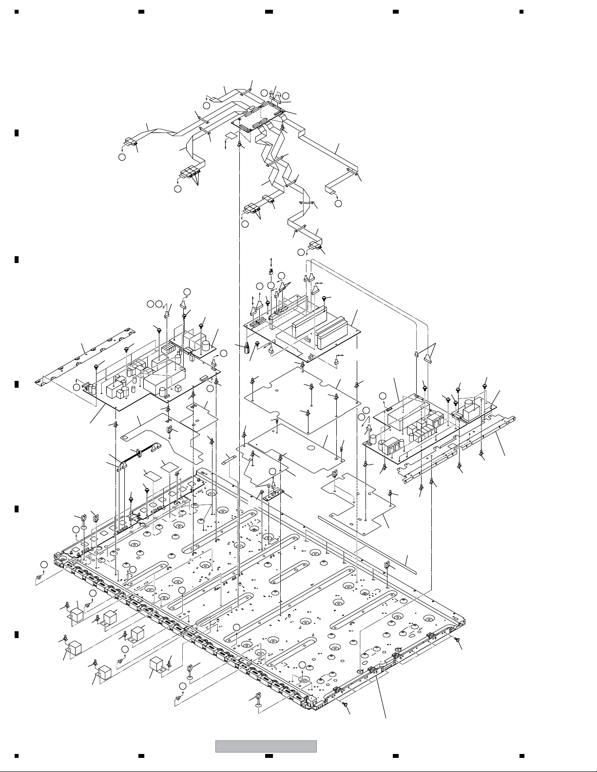
2.5 CHASSIS SECTION (2/2)
A
H
28
10
8, 31
A
12
28
MAIN
CN4001
28
9
20
G
F
19
5
32
32
34
11
28
46
E
42
AC inlet
44
7
18
28
N
16
1
32
E
O
46
46
47
32
32
32
32
32
46
32
32
47
2
24
38
33
C
MAIN
CN4008
46
14
F
Power
switch
8, 31
AUDIO
CN3751
K
46
8, 31
J
32
28
15
28
13
D
8, 31
MAIN
CN4002
B
17
8, 31
J
47
46
4
K
B
ML
C
23
46
46
47
32
32
32
32
37
32
G
39
27
6
32
40
32
H
44
32
28
32
26
29
I
32
32
41
32
3
D
27
30
I
22
21
27
47
35
47
27
36
29
25
L
E
M
43
32
32
32
43
32
43
F
32
43
A
B
43
N
32
30
43
O
C
D
27
47
30
47
Refer to
"2.6 PANEL CHASSIS SECTION".
18
PDP-5071PU
1234

5678
CHASSIS SECTION (2/2) PARTS LIST
No. Description Part No.
Mark
1 50 X MAIN DRIVE Assy AWW1143
2 50 X SUB DRIVE Assy AWW1144
3 50 Y MAIN DRIVE Assy AWW1145
4 50 Y SUB DRIVE Assy AWW1146
5 50 DIGITAL Assy AWW1139
6 SENSOR Assy AWW1140
7POWER SUPPLY Unit AXY1153
8Ferrite Core ATX1048
9 Flexible Cable (J201) ADD1435
10 Flexible Cable (J202) ADD1436
>
A
11 Flexible Cable (J206) ADD1440
12 Flexible Cable (J203) ADD1463
13 Flexible Cable (J205) ADD1465
14 Flexible Cable (J204) ADD1466
15 9P&6/5P Housing Wire (J101) ADX3337
16 8P&5P Housing Wire (J102) ADX3338
17 8P/4P Housing Wire (J108) ADX3339
18 8P/4P Housing Wire (J109) ADX3340
19 14P Housing Wire (J105) ADX3354
20 5P Housing Wire (J110) ADX3359
21 10P Housing Wire (J122) ADX3300
22 4P Housing Wire (J119) ADX3346
23 Conductive Plate Y ANG2902
24 Conductive Plate X ANG2905
25 Cushion AEB1424
26 Nyron Rivet AEC1671
27 Wire Saddle AEC1745
28 Flat Clamp AEC1879
29 PCB Support AEC1938
30 Harness Lifter 28 AEC1982
B
C
D
31 Ferrite Clamp AEC1986
32 Re-use PCB Spacer AEC2087
33 Tapping Card Spacer AEC2103
34 Flat Clamp 60 AEC2104
35 Drive Silicone Sheet B AEH1109
36 Drive Silicone Sheet C AEH1110
37 Power Supply Sheet B (507) AMR3555
38 Address Sheet A AMR3628
39 Address Sheet B AMR3629
40 Address Sheet E AMR3645
41 Address Sheet F AMR3646
42 Power Supply Sheet (507) AMR3634
43 Gasket AV8 ANK1881
44 Rivet A BEC1158
45 • • • • •
46 Screw ABA1313
47 Screw ABA1364
56
PDP-5071PU
E
F
19
7
8
1234
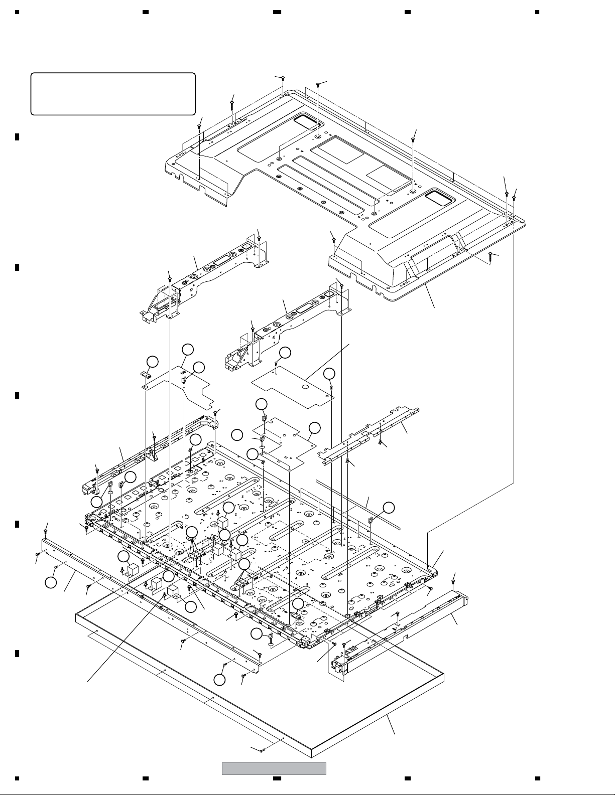
2.6 PANEL CHASSIS SECTION
A
B
6
7
5
7
10
7
7
4
7
2
11
C
10
7
D
3
7
7
1
9
E
F
20
1234
PDP-5071PU
8

5678
PANEL CHASSIS SECTION PARTS LIST
No. Description Part No.
Mark
NSP 1 Panel Chassis (507) Assy AWU1148
NSP 2 Plasma Panel (50DC) Assy AWU1162
NSP 3 50 ADDRESS L Assy AWW1141
NSP 4 50 ADDRESS S Assy AWW1142
NSP 5 50 SCAN A Assy AWW1147
NSP 6 50 SCAN B Assy AWW1148
7 Re-use PCB Spacer AEC2088
NSP 8 Adhesive Tape (50) AEH1119
9 Conductive Plate Holder AMR3446
10 Screw ABA1351
A
NSP 11 Tube Cover AMR3445
B
C
D
56
PDP-5071PU
E
F
21
7
8
1234
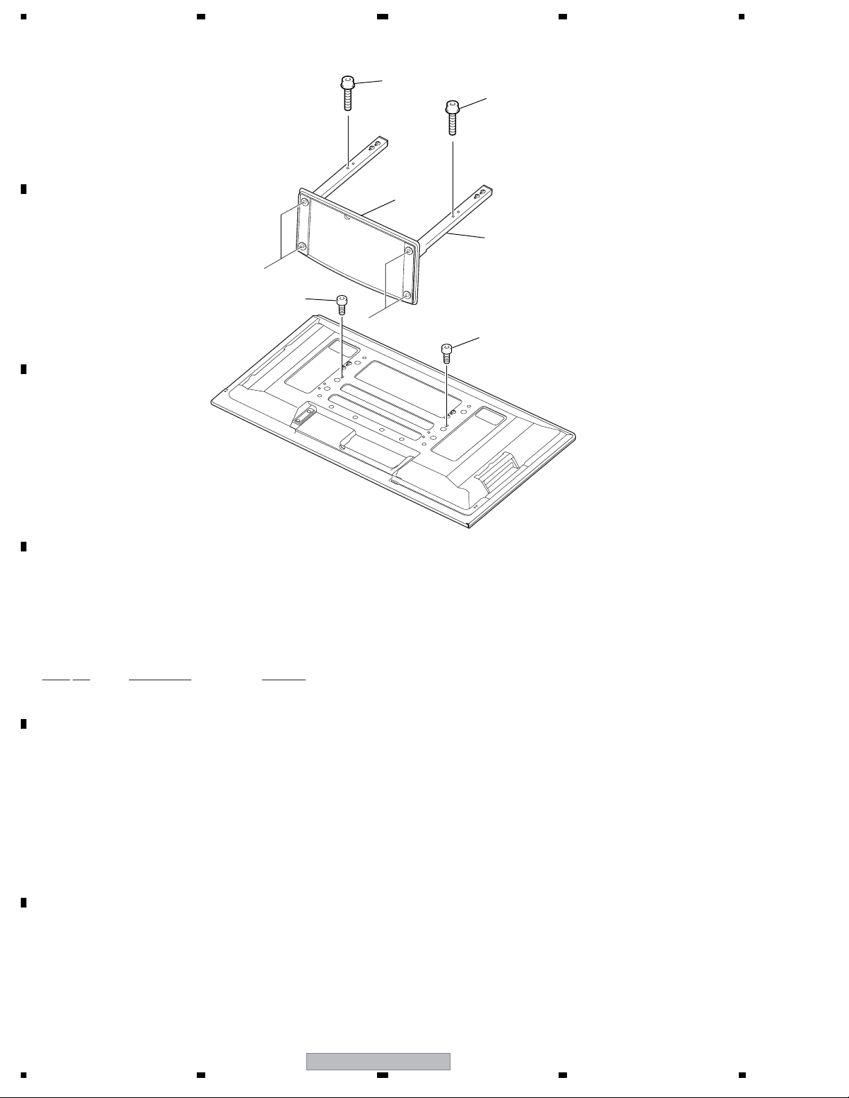
2.7 MULTIBASE SECTION
A
SIDE KEY CN9501
LED IR CN9701
A
13
51
20
51
31
D
50 DIGITAL
CN3001
POWER
P8
17
POWER
P9
USB
(side)
E
G
F
Fan
51
44
44
43
51
51
8
B
50 LED
B
C
7
51
1
CN9651
D
20
7
51
14
39
3
48
15
F
E
7
POWER
P3
46
32
38
51
31
15
48
C
51
4
D
23
33
5
37
19
33
47
46
21
49
35
A
47
50
18
30
24
46
48
POWER
P5
46
46
10
52
6
27
26
25
E
51
51
45
45
11
B
C
30
30
26
25
28
9
16
G
12
F
2
SIDE
CN9101
30
29
22
36
22
PDP-5071PU
1234

5678
MULTIBASE SECTION PARTS LIST
No. Description Part No.
Mark
1 MAIN Assy AWV2312
2TANSHI Assy AWW1156
3 POD Assy AWW1154
4AUDIO Assy AWW1131
5 SP TERMINAL Assy AWW1132
>
>
>
No. Description Part No.
Mark
41 • • • • •
42 • • • • •
43 Gasket UB ANK1867
44 Tuner Shield ANK1875
45 Locking Card Spacer AEC2093
A
6Ferrite Core ATX1044
7Ferrite Core ATX1048
8Ferrite Core ATX1064
9Power Switch (S2)(TRAP) ASG1089
10 AC Inlet (CN1) AKP1301
11 Flexible Cable (J210) ADD1441
12 Flexible Cable (J211) ADD1442
13 Flexible Cable (J207) ADD1445
14 Flexible Cable (J213) ADD1446
15 Flexible Cable (J214)(J215) ADD1447
16 3P Housing Wire (J121) ADX3348
17 13P&11P Housing Wire (J106) ADX3355
18 3P Housing Wire (J107) ADX3356
19 11P Housing Wire (J111) ADX3360
20 7/6/4/3P Housing Wire (J113) ADX3341
21 Housing Wire (J104) ADX3353
22 14P Housing Wire (J116) ADX3344
23 8/4P Housing Wire (J117) ADX3345
24 Binder AEC-093
25 Locking Card Spacer AEC1429
26 Wire Saddle AEC1745
27 Ferrite Core Holder AEC1818
28 Clamp AEC1884
29 Card Spacer AEC1889
30 Re-use Wire Saddle AEC1945
46 Screw AMZ30P060FTB
47 Hex. Head Screw BBA1051
48 Nut BBN1005
49 Screw BMZ30P060FTB
50 Screw BPZ30P080FTB
51 Screw PMB30P080FNI
52 Inlet Spacer AEC2112
B
C
D
31 Ferrite Stopper AEC1981
32 Ferrite Clamp AEC1986
33 Locking Card Spacer AEC2019
34 • • • • •
35 POD Cover AMR3542
36 Multi Base (U) Assy ANA1951
37 Terminal Panel A (U/B) ANC2394
38 POD Stay A ANG2933
39 Tuner Stay U ANG3028
40 • • • • •
56
PDP-5071PU
E
F
23
7
8
1234
2.8 PDP SERVICE ASSY 507 (AWU1212)
A
Note:
The parts labeled here with circled numbers
are supplied with the Assy for service.
Attach them, referring to this diagram.
B
C
18
36
21
4
35 ×2
12
32
36
36 ×4
36
5
27
35 ×2
35 ×2
35 ×2
36
29
Power supply sheet B (507)
This is not included in the Assy for service.
Detach it from the product to be repaired
and attach it to the Assy for service.
27
36 ×4
36 ×4
32
33
2
33 ×5
6
35
33
17
33 ×4
26
12
×2
D
48
47
E
F
11
Re-use PCB Spacer
This spacer is used for attaching the
Gasket AV8, and is not included in the Assy
for service. Remove the 6 PCB Spacers from
the product to be repaired and attach them to
the Assy for service.
26
35
26
18
15
×3
33 ×4
11
33
26
26
33 ×5
17
14
47
26
18
×4
×2
48
15
12
×2
20
19
9
×3
18
17
34 ×4
33
7
19
12
×5
34 ×4
33
28
(for transport)
1
33
3
24
PDP-5071PU
1234
5678
Packing Section
41
45
40
46
42
44
43
10 ×4, 11 ×2, 12 ×11,
13 ×9, 15 ×2, 16 ×2,
17 ×4, 18 ×10, 25 ×2,
26 ×6, 27 ×2, 36 ×1
8
37
38 38 39 39
20 to 24
(*)
No. Part Name Part No.
8 Clamp base ANG3030 ×1 Not used
10 PCB spacer AEC1126 ×4 Not used
12 Wire saddle AEC1745 ×11
13 Wire saddle AEC1751 ×9 Not used
15 PCB support AEC1938 ×2
16 PCB support AEC1958 ×2 Not used
17 Harness lifter 28 AEC1982 ×4
18 Ferrite clamp AEC1986 ×10
22 DC sheet A AMR3612 ×1 Not used
23 Address sheet E AMR3621 ×1 Not used
24 Address sheet D AMR3631 ×1 Not used
25 Gasket E ANK1874 ×2 Not used
36 Screw
TBZ40P080FTB
No. of
pcs
Ten of the 11 wire saddles are to be used
with this unit. Attach them to the places
where T indications are engraved.
Attach them to the places where C
indications are engraved.
Attach them to the places where U
indications are engraved.
Eight of the 10 ferrite clamps are to be
used with this unit.
Twelve screws have been already
secured to the Assy.
×13
The remaining one screw packed in a
plastic bag is not used with this unit.
Remarks
A
B
PDP SERVICE ASSY 507 (AWU1212) PARTS LIST
No. Description Part No.
Mark
NSP 1 Panel Chassis (507) Assy AWU1148
2Front Chassis VL (50) AMA1014
3Front Chassis VR (507) AMA1022
4 Sub Frame L Assy 507 ANA1945
5 Sub Frame R Assy 507 ANA1946
6Front Chassis H Assy (507) ANA2031
7 Conductive Plate X ANG2905
8 Clamp Base ( * ) ANG3030
9 Cushion AEB1424
NSP 10 PCB Spacer ( * ) AEC1126
11 PCB Spacer AEC1570
12 Wire Saddle ( * ) AEC1745
13 Wire Saddle ( * ) AEC1751
14 Screw Rivet AEC1877
15 PCB Support ( * ) AEC1938
16 PCB Support ( * ) AEC1958
17 Harness Lifter 28 ( * ) AEC1982
18 Ferrite Clamp ( * ) AEC1986
19 Re-use PCB Spacer AEC2087
20 Address Sheet A AMR3628
No. Description Part No.
Mark
26 Gasket AV8 ANK1881
27 Rivet A BEC1158
NSP 28 Front Case Assy (507SV) AMB2977
29 Rear Case (507) ANE1656
30 Caution Label AAX3031
NSP 31 Drive Voltage Label ARW1097
32 Screw (3 x 40P) ABA1332
33 Screw ABA1351
34 Screw ABA1364
35 Screw AMZ30P060FTB
36 Screw ( * ) TBZ40P080FTB
37 Polyethylene Bag AHG1337
38 Polyethylene Bag S AHG1338
39 Polyethylene Bag AHG1340
40 Pad (507 T-L) AHA2538
41 Pad (507 T-R) AHA2539
42 Pad (507 B-L) AHA2540
43 Pad (507 B-R) AHA2541
44 Under Carton (507) AHD3473
45 Upper Carton (507SV) AHD3550
C
D
E
21 Address Sheet F AMR3646
22 DC Sheet A ( * ) AMR3612
23 Address Sheet E ( * ) AMR3621
24 Address Sheet D ( * ) AMR3631
25 Gasket E ( * ) ANK1874
56
46 Protect Sheet AHG1331
47 Screw ABZ30P080FTC
48 Screw APZ30P080FTB
PDP-5071PU
F
25
7
8
1234
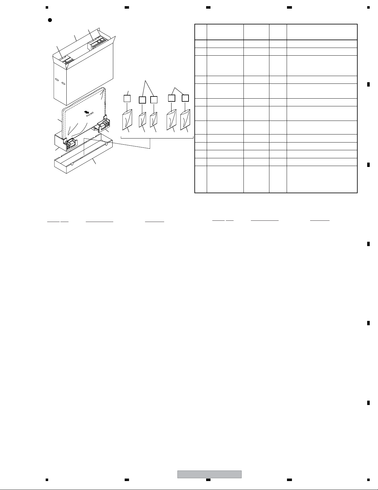
2.9 TABLE TOP STAND
A
4
4
2
1
B
C
D
TABLE TOP STAND PARTS LIST
Mark
No. Description Part No.
NSP 1 Stand Pipe Assy AXY1141
NSP 2 Base Cover Assy AXY1142
3 Bolt (HEX) ABA1358
4 Bolt (HEX) ABA1359
5 Screw ABA1360
5
3
5
3
E
F
26
1234
PDP-5071PU

5678
3. PCB PARTS LIST
>
NOTES:
Parts marked by "NSP" are generally unavailable because they are not in our Master Spare Parts List.
The mark found on some component parts indicates the importance of the safety factor of the part.
Therefore, when replacing, be sure to use parts of identical designation.
When ordering resistors, first convert resistance values into code form as shown in the following examples.
Ex.1 When there are 2 effective digits (any digit apart from 0), such as 560 ohm and 47k ohm (tolerance is shown by J=5%,
and K=10%).
560 Ω
47k Ω
0.5 Ω
1 Ω
56 x 10
47 x 10
R50
1R0
1
3
Ex.2 When there are 3 effective digits (such as in high precision metal film resistors).
5.62k Ω
1
Mark No. Description Part No.
LIST OF ASSEMBLIES
NSP 1..PANEL CHASSIS (507) ASSY AWU1148
NSP 2..50 ADDRESS ASSY AWV2303
NSP 3..50 ADDRESS L ASSY AWW1141
NSP 3..50 ADDRESS S ASSY AWW1142
NSP 2..50 SCAN ASSY AWV2304
NSP 3..50 SCAN A ASSY AWW1147
NSP 3..50 SCAN B ASSY AWW1148
NSP 1..50 X DRIVE ASSY AWV2305
2..50 X MAIN DRIVE ASSY AWW1143
2..50 X SUB DRIVE ASSY AWW1144
NSP 1..50 Y DRIVE ASSY AWV2306
2..50 Y MAIN DRIVE ASSY AWW1145
2..50 Y SUB DRIVE ASSY AWW1146
NSP 1..50 DIGITAL ASSY AWV2302
2..50 DIGITAL ASSY AWW1139
2..SENSOR ASSY AWW1140
1..MAIN ASSY (US BB) AWV2312
NSP 1..I/O ASSY AWV2313
2..POD ASSY AWW1154
2..TANSHI ASSY AWW1156
2..SIDE ASSY AWW1157
NSP 1..50 AUDIO FUKUGO ASSY AWV2346
2..AUDIO ASSY AWW1131
2..SP TERMINAL ASSY AWW1132
2..SIDE KEY ASSY AWW1133
2..50 LED ASSY AWW1135
2..LED IR ASSY AWW1136
1..POWER SUPPLY UNIT AXY1153
Mark No. Description Part No.
50 DIGITAL ASSY
[DIGITAL IF BLOCK]
MISCELLANEOUS
F3001 CCG1162
CN3001 50P CONNECTOR AKM1353
CN3002 20P FFC CONNECTOR AKM1235
RESISTORS
R3007, 3010–3016 RAB4C470J
R3020–3022 RAB4C103J
Other Resistors RS1/16SS###J
56
561
473
5621
Mark No. Description Part No.
[MODULE UCOM BLOCK]
SEMICONDUCTORS
IC3151 AGC1011
IC3152, 3153 SN74AHC541PW
IC3155 SN74AHC08PW
IC3156 BR24L04FJ-W
IC3157 M62334FP
IC3159 TC7W126FU
IC3160, 3161 TC74VHC123AFTS1
Q3151 2SJ461A
D3151, 3152, 3154, 3155 DAN202U
D3158, 3159, 3161–3163 1SS355
MISCELLANEOUS
X3151 CSS1616
CN3151 CONNECTOR AKM1276
CN3152 CONNECTOR CKS4828
RESISTORS
R3155, 3160, 3170, 3176 RAB4C101J
R3174 RAB4C103J
Other Resistors RS1/16SS###J
CAPACITORS
C3151 CEHVKW470M6R3
C3152, 3153, 3155–3158 CKSSYB104K10
C3159, 3171, 3172, 3182 CKSRYB105K6R3
C3162, 3163, 3165, 3166 CKSSYB104K10
C3164 CCSSCH101J50
C3167 CKSSYB103K16
C3168, 3170, 3181 CKSSYB104K10
[PANEL FLASH BLOCK]
SEMICONDUCTORS
IC3301 AGC1009
IC3302, 3305 PST3628UR
IC3303 SN74AHC08PW
IC3304 PST3610UR
Q3301 RN1901
Q3302 HN1C01FU
MISCELLANEOUS
X3302 ASS1188
CN3301 CONNECTOR CKS4835
RESISTORS
R3307, 3308 RAB4C101J
PDP-5071PU
RD1/4PU J
RD1/4PU J
RN2H K
RS1P K
RN1/4PC F562 x 10
7
A
561
473
R50
1R0
5621
B
C
D
E
F
27
8

1234
Mark No. Description Part No.
Other Resistors RS1/16SS###J
A
CAPACITORS
C3301–3303, 3306, 3308 CKSSYB104K10
C3304, 3307, 3309 CKSSYB472K16
C3305, 3310 CKSSYB102K50
C3311 CCSRCH470J50
C3315, 3316 CKSSYB104K10
C3317 CCSRCH471J50
[SQ ASIC BLOCK]
SEMICONDUCTORS
IC3401 PEG239A
B
MISCELLANEOUS
L3401–3403 QTL1013
F3401, 3402 CCG1162
Mark No. Description Part No.
SENSOR ASSY
SEMICONDUCTORS
IC3651 MM1522XU
IC3652 BR24L02FJ-W
Q3651 HN1B04FU
MISCELLANEOUS
CN3651 CONNECTOR AKM1276
RESISTORS
Other Resistors RS1/16SS###J
CAPACITORS
C3651, 3653 CKSRYB105K6R3
C3652, 3654 CKSSYB103K16
C3656, 3657 CKSSYB104K10
RESISTORS
R3402, 3412 RAB4C101J
R3405–3407, 3409, 3410 RAB4C220J
R3416 RAB4C220J
R3425 RS1/16SS5601F
Other Resistors RS1/16SS###J
C
CAPACITORS
C3401, 3402, 3419, 3425 CEHVKW101M6R3
C3403–3413, 3417, 3418 CKSSYB104K10
C3420–3424, 3426–3432 CKSSYB104K10
C3445–3448 CKSSYB104K10
[ADDRESS CN BLOCK]
SEMICONDUCTORS
Q3501, 3502 RN1901
D3501, 3502 DAN202U
MISCELLANEOUS
D
CN3501–3504, 3506
CN3505 18P CONNECTOR VKN1310
40P CONNECTOR
AKM1348
RESISTORS
R3519, 3520 RAB4C472J
R3521, 3522, 3525 RAB4C101J
R3524 RAB4C222J
Other Resistors RS1/16SS###J
[DIGITAL DD CON BLOCK]
SEMICONDUCTORS
E
IC3601 BA80BC0WFP
MISCELLANEOUS
U3601 DD CON UNIT AXY1137
RESISTORS
R3611 RAB4C101J
Other Resistors RS1/16SS###J
CAPACITORS
C3609 CKSSYB104K10
C3611 CKSQYB105K16
F
C3612 ACH1394
C3613 CKSSYB103K16
50 X MAIN DRIVE ASSY
[50X LOGIC BLOCK]
SEMICONDUCTORS
IC1001 TC74ACT541FT
IC1002 TC74VHC00FTS1
D1001–1004 1SS355
MISCELLANEOUS
K1004, 1007 TEST PIN AKX1061
CN1001 18P CONNECTOR VKN1310
RESISTORS
R1001, 1006 RAB4C470J
R1004 RAB4C472J
VR1001 CCP1390
Other Resistors RS1/16S###J
CAPACITORS
C1001 CEHAT470M16
C1002, 1003 CKSRYB104K16
C1004 CCSRCH331J50
C1006 CCSRCH680J50
[50X RESONANCE BLCOK]
SEMICONDUCTORS
IC1101, 1105 TND307TD
IC1102 PS9117P
IC1104 AXF1163
IC1107 PS2701A-1(L)
Q1101 2SC2412K
Q1102, 1103 QSZ2
Q1104, 1105 2SC4081
D1101, 1103 UDZS5R6(B)
D1102 CRH01
D1104 UDZS15(B)
MISCELLANEOUS
L1101 ATH1217
L1106 ATH1216
F1101 CTF1449
1101 ANH1653
1102 AEH1092
1103 BMZ30P080FTC
28
PDP-5071PU
1234

5678
Mark No. Description Part No.
RESISTORS
R1107, 1108 RS3LMF100J
R1109, 1110 RS1/10S4702F
R1113 RS1/16S1002F
R1114 RS1/16S3302F
R1115 ACN1259
Mark No. Description Part No.
CAPACITORS
C1201, 1212 ACG1126
C1202, 1209, 1232, 1236 CKSRYB104K16
C1203, 1208, 1215, 1229 CKSRYF104Z50
C1205, 1206, 1217, 1218 ACG1139
C1207, 1214, 1220, 1226 CEHAT470M25
A
R1119 ACN1258
R1121 RS1/16S4701F
Other Resistors RS1/16S###J
CAPACITORS
C1101, 1114 CEHAT470M25
C1102, 1115 CKSRYF104Z50
C1103 CKSRYB104K16
C1104, 1117 CKSYB105K25
C1107, 1116 ACG1126
C1113 ACH1450
C1121–1124 ACE1178
[50X SUS BLOCK]
SEMICONDUCTORS
IC1201, 1204, 1206, 1208 TND307TD
IC1202, 1205 PS9117P
IC1209 MM1565AF
Q1201, 1208 2SC2412K
Q1202, 1204, 1205, 1207 H5N2512LS
Q1209, 1212–1214 QSZ2
Q1210, 1211 FKP280AS
Q1215, 1221 FKP300AS
Q1216 DTC143EK
Q1217 DTC123TKA
Q1220 R5009ANJ
D1201, 1205 UDZS5R6(B)
D1202, 1203, 1206, 1211 CRH01
D1204 D1FL40
D1208 1SS302
D1209 UDZS16(B)
D1210 1SS355
D1212 CRH01
D1213 UDZS8R2(B)
MISCELLANEOUS
L1201, 1203, 1204 BTH1134
L1202 ATH1186
F1227 CTF1449
K1202 TEST PIN AKX1061
KN1201–1204, 1210–1217 ANK1841
CN1201 14P CONNECTOR 14PL-FJ
CN1204 8P TOP POST B8B-EH
1202 SCREW PMB30P080FNI
C1210, 1211, 1216, 1241 CKSYB105K25
C1213 CCSRCH221J50
C1222, 1223 ACH1423
C1224, 1225 ACE1178
C1228 CEHAT2R2M2E
C1230 ACH1449
C1231, 1237 CEHAT101M10
C1233 CKSRYB473K16
C1234 CEHAT470M16
C1235 CKSRYB105K6R3
C1244 CKSRYB104K25
[DRIVE HEAT SINK M]
MISCELLANEOUS
3001, 3001 ANH1656
3001 ANH1656
3101, 3101 ANG2679
3101 ANG2679
[50X D-D CON BLOCK]
SEMICONDUCTORS
IC1301 PS2701A-1(L)
IC1302 TA76431FR
Q1301 2SC2412K
Q1303, 1306, 1307 HN1C01FU
Q1304, 1401 2SD1898
Q1305 2SA1037K
Q1402 2SC4081
D1307 CRF03
D1308, 1403 UDZS5R1(B)
D1309, 1311, 1401, 1405 CRH01
D1312, 1402 1SS301
D1313, 1318, 1404, 1406 1SS355
D1315, 1316 UDZS4R7(B)
MISCELLANEOUS
T1302 ATK1160
T1401 ATK1159
RESISTORS
R1312–1314, 1317 RS1/10S224J
R1328 RAB4C472J
VR1301 CCP1392
Other Resistors RS1/16S###J
B
C
D
E
RESISTORS
R1208, 1210, 1213, 1215 RS1/10S100J
R1211 ACN1254
R1219, 1228, 1230, 1231 RS1/10S0R0J
R1220, 1224, 1233, 1256 RS1/10S2R2J
R1237 RS1/10S0R0J
R1239 ACN1258
R1245 ACN1257
R1247, 1248 RS3LMF470J
Other Resistors RS1/16S###J
56
CAPACITORS
C1301, 1302, 1405, 1406 CKSRYB104K16
C1308, 1401, 1407 CEHAT101M25
C1310, 1313, 1402 CKSYB105K25
C1311 ACH1451
C1312, 1403 CKSRYB103K50
C1314 CEHAT100M50
C1404 ACG1105
PDP-5071PU
F
29
7
8

1234
Mark No. Description Part No.
50 X SUB DRIVE ASSY
SEMICONDUCTORS
Q1501 FKP280AS
A
Q1502 FKP300AS
Q1504, 1505 H5N2512LS
Q1507 QSZ2
D1501 CRH01
Mark No. Description Part No.
IC2107 AXF1163
Q2101 2SC2412K
Q2103, 2106 QSZ2
Q2110, 2111 2SC4081
D2101, 2112 UDZS5R6(B)
D2107 CRH01
D2113 UDZS15(B)
MISCELLANEOUS
K1501 TEST PIN AKX1061
KN1501–1505 GROUND PLATE ANK1841
CN1501 14P CONNECTOR 14R-FJ
1502 SCREW PMB30P080FNI
RESISTORS
B
R1502, 1503 RS1/10S2R2J
R1507, 1508 RS1/10S100J
Other Resistors RS1/16S###J
CAPACITORS
C1501 ACE1178
C1503, 1504 ACG1139
C1505 ACH1423
C1506 CKSYB105K25
[DRIVE HEAT SINK M]
MISCELLANEOUS
C
3001, 3001 ANH1656
3101, 3101 ANG2679
RESISTORS
Other Resistors RS1/16S###J
50 Y MAIN DRIVE ASSY
[50Y LOGIC BLOCK]
SEMICONDUCTORS
IC2001, 2003 TC74ACT541FT
D
IC2002 TC74ACT540FT
D2001, 2006, 2007, 2011 1SS355
D2003–2005 1SS301
D2012 1SS355
MISCELLANEOUS
K2011, 2014 TEST PIN AKX1061
CN2001 40P CONNECTOR AKM1348
RESISTORS
R2001, 2003, 2008, 2020 RAB4C470J
R2002, 2006 RAB4C101J
E
R2004, 2005, 2013, 2025 RAB4C472J
VR2001, 2002 CCP1390
Other Resistors RS1/16S###J
CAPACITORS
C2001 CEHAT470M16
C2002–2004 CKSRYB104K16
C2005, 2006 CCSRCH331J50
C2007 CCSRCH680J50
[50Y RESONANCE BLCOK]
SEMICONDUCTORS
F
IC2101, 2104 TND307TD
IC2102 PS9117P
IC2106 PS2701A-1(L)
30
1234
MISCELLANEOUS
L2101 ATH1217
L2103 ATH1216
F2101 CTF1449
2101 ANH1653
2102 AEH1092
2103 SCREW BMZ30P080FTC
RESISTORS
R2109 ACN1259
R2112, 2133 ACN1255
R2113, 2114 RS1/10S4702F
R2118 ACN1241
R2120 RS1/16S1002F
R2121 RS1/16S3302F
R2126 RS1/16S4701F
R2129 ACN1258
Other Resistors RS1/16S###J
CAPACITORS
C2101, 2114 CEHAT470M25
C2102, 2115 CKSRYF104Z50
C2103 CKSRYB104K16
C2104, 2116 CKSYB105K25
C2107 ACG1139
C2108–2111 ACE1178
C2113 ACH1450
C2117 ACG1138
[50Y SUS BLOCK]
SEMICONDUCTORS
IC2201, 2203, 2205, 2208 TND307TD
IC2204, 2209 PS9117P
IC2210 TND307TD
IC2212 TND301S
IC2213 MM1565AF
Q2201 2SA2142
Q2202, 2214 2SC4081
Q2203 R5009ANJ
Q2204, 2206, 2207, 2209 H5N2512LS
Q2210, 2216 FKP280AS
Q2211, 2213, 2217, 2219 H5N2512LS
Q2215, 2221, 2222, 2241 QSZ2
Q2220, 2223 FKP300AS
Q2236 2SK3050
Q2238 R6008ANJ
Q2261 DTC143EK
Q2262 DTC123TKA
D2201, 2202, 2204, 2209 CRH01
D2203, 2225 1SS355
D2205, 2206 1SS302
D2207 CRF03
D2208, 2212 UDZS5R6(B)
D2210, 2213, 2216 CRH01
PDP-5071PU
 Loading...