

Page 1
PIONEER CORPORATION 4-1, Meguro 1-chome, Meguro-ku, Tokyo 153-8654, Japan
PIONEER ELECTRONICS (USA) INC. P.O. Box 1760, Long Beach, CA 90801-1760, U.S.A.
PIONEER EUROPE NV Haven 1087, Keetberglaan 1, 9120 Melsele, Belgium
PIONEER ELECTRONICS ASIACENTRE PTE. LTD. 253 Alexandra Road, #04-01, Singapore 159936
PIONEER CORPORATION 2005
Note:
Media Receivers up to Generation 5 (G5) cannot be connected with this unit.
Be sure to use a Media Receiver of Generation 6 (G6) (ex.: PDP-R06∗∗, etc.).
ORDER NO.
ARP3267
PDP-506PE
PLASMA DISPLAY
PDP-506PE
PDP-506PU
THIS MANUAL IS APPLICABLE TO THE FOLLOWING MODEL(S) AND TYPE(S).
Model Type Power Requirement Remarks
PDP-506PE WYVI AC220 - 240V
PDP-506PU KUCXC AC120V
This service manual should be used together with the following manual(s).
Model No. Order No. Remarks
PDP-506PE, PDP-506PU ARP3268 SCHEMATIC DIAGRAM, PCB CONNECTION DIAGRAM
For details, refer to "Important Check Points for good servicing".
T-IZY SEPT. 2005 printed in Japan
Page 2

1234
SAFETY INFORMATION
A
This service manual is intended for qualified service technicians ; it is not meant for the casual
do-it-yourselfer. Qualified technicians have the necessary test equipment and tools, and have been
trained to properly and safely repair complex products such as those covered by this manual.
Improperly performed repairs can adversely affect the safety and reliability of the product and may
void the warranty. If you are not qualified to perform the repair of this product properly and safely,
you should not risk trying to do so and refer the repair to a qualified service technician.
WARNING
This product contains lead in solder and certain electrical parts contain chemicals which are known to the state of California to
B
cause cancer, birth defects or other reproductive harm.
NOTICE
(FOR CANADIAN MODEL ONLY)
Fuse symbols (fast operating fuse) and/or (slow operating fuse) on PCB indicate that replacement parts
must be of identical designation.
Health & Safety Code Section 25249.6 - Proposition 65
REMARQUE
(POUR MODÈLE CANADIEN SEULEMENT)
Les symboles de fusible (fusible de type rapide) et/ou (fusible de type lent) sur CCI indiquent que les pièces
C
de remplacement doivent avoir la même désignation.
SAFETY PRECAUTIONS
NOTICE : Comply with all cautions and safety related notes
located on or inside the cabinet and on the chassis.
The following precautions should be observed :
1. When service is required, even though the PDP UNIT an
isolation transformer should be inserted between the power line
D
and the set in safety before any service is performed.
2. When replacing a chassis in the set, all the protective devices
must be put back in place, such as barriers, nonmetallic knobs,
adjustment and compartment covershields, isolation resistorcapacitor, etc.
3. When service is required, observe the original lead dress. Extra
precaution should be taken to assure correct lead dress in the
high voltage circuitry area.
4. Always use the manufacture's replacement components.
Especially critical components as indicated on the circuit
diagram should not be replaced by other manufacture's.
Furthermore where a short circuit has occurred, replace those
E
components that indicate evidence of overheating.
5. Before returning a serviced set to the customer, the service
technician must thoroughly test the unit to be certain that it is
completely safe to operate without danger of electrical shock,
and be sure that no protective device built into the set by the
manufacture has become defective, or inadvertently defeated
during servicing. Therefore, the following checks should be
performed for the continued protection of the customer and
servicetechnician.
6. Perform the following precautions against unwanted radiation
and rise in internal temperature.
• Always return the internal wiring to the original styling.
• Attach parts (Gascket, Ferrite Core, Ground, Rear Cover,
Shield Case etc.) surely after disassembly.
7. Perform the following precautions for the PDP panel.
• When the front case is removed, make sure nothing hits the
panel face, panel corner, and panel edge (so that the glass does
not break).
• Make sure that the panel vent does not break. (Check that the
cover is attached.)
• Handle the FPC connected to the panel carefully.
Twisting or pulling the FPC when connecting it to the
connector will cause it to peel off from the panel.
8. Pay attention to the following.
• Pay extreme caution when the front case and rear panel are
removed because this may cause a high risk of disturbance to
TVs and radios in the surrounding.
F
2
1234
PDP-506PE
Page 3
5678
Leakage Current Cold Check
With the AC plug removed from an AC power source, place a
jumper across the two plug prongs. Turn the AC power switch on.
Using an insulation tester (DC 500V), connect one lead to the
jumpered AC plug and touch the other lead to each exposed metal
part (input/output terminals, screwheads, metal overlays, control
shafts, etc.), particularly any exposed metal part having a return
path to the chassis. Exposed metal parts having a return path to
the chassis should have a minimum resistor reading of 0.3MΩ
and a maximum resistor reading of 5MΩ. Any resistor value
below or above this range indicates an abnormality which requires
corrective action. Exposed metal parts not having a return path to
the chassis will indicate an open circuit.
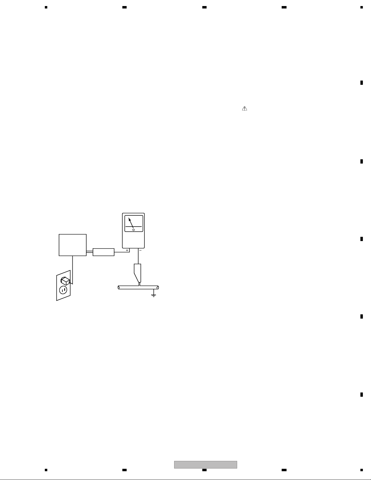
Leakage Current Hot Check
Plug the AC line cord directly into an AC power source (do not
use an isolation transformer for this check).
Turn the AC power switch on.
Using a "Leakage Current Tester (Simpson Model 229
equivalent)", measure for current from all exposed metal parts of
the cabinet (input/output terminals, screwheads, metal overlays,
control shaft, etc.), particularly any exposed metal part having a
return path to the chassis, to a known earth ground (water pipe,
conduit, etc.). Any current measured must not exceed 0.5mA.
PRODUCT SAFETY NOTICE
Many electrical and mechanical parts in PIONEER set have
special safety related characteristics. These are often not evident
from visual inspection nor the protection afforded by them
necessarily can be obtained by using replacement components
rated for higher voltage, wattage, etc. Replacement parts which
have these special safety characteristics are identified in this
Service Manual.
Electrical components having such features are identified by
marking with a on the schematics and on the parts list in this
Service Manual.
The use of a substitute replacement component which dose not
have the same safety characteristics as the PIONEER
recommended replacement one, shown in the parts list in this
Service Manual, may create shock, fire or other hazards.
Product Safety is continuously under review and new instructions
are issued from time to time. For the latest information, always
consult the current PIONEER Service Manual. A subscription to,
or additional copies of, PIONEER Service Manual may be
obtained at a nominal charge from PIONEER.
A
B
C
Reading should
not be above
0.5mA
Earth
ground
Device
under
test
Also test with
plug reversed
(Using AC adapter
plug as required)
Leakage
current
tester
Test all
exposed metal
surfaces
AC Leakage Test
ANY MEASUREMENTS NOT WITHIN THE LIMITS
OUTLINED ABOVE ARE INDICATIVE OF A POTENTIAL
SHOCK HAZARD AND MUST BE CORRECTED BEFORE
RETURNING THE SET TO THE CUSTOMER.
D
E
56
PDP-506PE
F
3
7
8
Page 4
1234
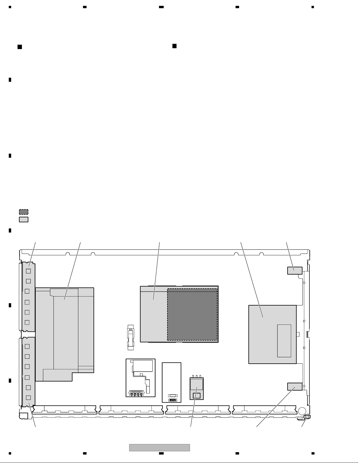
A
Charged Section
The places where the commercial AC power is used without
passing through the power supply transformer.
If the places are touched, there is a risk of electric shock. In
addition, the measuring equipment can be damaged if it is
connected to the GND of the charged section and the GND of the
non-charged section while connecting the set directly to the
commercial AC power supply. Therefore, be sure to connect the
set via an insulated transformer and supply the current.
B
1. Power Cord
2. AC Inlet
3. Power Switch (S1)
4. Fuse (In the POWER SUPPLY Unit)
5. STB Transformer and Converter Transformer
(In the POWER SUPPLY Unit)
6. Other primary side of the POWER SUPPLY Unit
C
: Part is Charged Section.
: Part is the High Voltage Generating Points
other than the Charged Section.
High Voltage Generating Point
The places where voltage is 100V or more except for the charged
places described above. If the places are touched, there is a risk of
electric shock.
If the procedures described in “7.1.5 POWER ON/OFF
FUNCTION FOR THE LARGE-SIGNAL SYSTEM” are
performed before the power is turned off, the voltage will be
discharged in about 30 seconds.
1. POWER SUPPLY Unit.....................................................(205V)
2. 50 X DRIVE Assy .......................................... (–180V to 205V)
3. 50 Y DRIVE Assy .......................................................... (500V)
4. 50 SCAN A Assy ............................................................ (500V)
5. 50 SCAN B Assy ............................................................(500V)
6. SUS CLAMP 1 Assy .......................................(–180V to 205V)
7. SUS CLAMP 2 Assy .......................................(–180V to 205V)
50 SCAN B Assy
D
E
50 Y DRIVE Assy 50 X DRIVE Assy SUS CLAMP 1 Assy
POWER SUPPLY Unit
F
50 SCAN A Assy SUS CLAMP 2 Assy Power Switch (S1)
AC Inlet
Fig.1 Charged Section and High Voltage Generating Point (Rear View)
4
1234
PDP-506PE
Page 5
5678
[Important Check Points for Good Servicing]
In this manual, procedures that must be performed during repairs are marked with the below symbol.
Please be sure to confirm and follow these procedures.
1. Product safety
Please conform to product regulations (such as safety and radiation regulations), and maintain a safe servicing environment by
following the safety instructions described in this manual.
1 Use specified parts for repair.
Use genuine parts. Be sure to use important parts for safety.
2 Do not perform modifications without proper instructions.
Please follow the specified safety methods when modification(addition/change of parts) is required due to interferences such as
radio/TV interference and foreign noise.
3 Make sure the soldering of repaired locations is properly performed.
When you solder while repairing, please be sure that there are no cold solder and other debris.
Soldering should be finished with the proper quantity. (Refer to the example)
4 Make sure the screws are tightly fastened.
Please be sure that all screws are fastened, and that there are no loose screws.
5 Make sure each connectors are correctly inserted.
Please be sure that all connectors are inserted, and that there are no imperfect insertion.
6 Make sure the wiring cables are set to their original state.
Please replace the wiring and cables to the original state after repairs.
In addition, be sure that there are no pinched wires, etc.
7 Make sure screws and soldering scraps do not remain inside the product.
Please check that neither solder debris nor screws remain inside the product.
8 There should be no semi-broken wires, scratches, melting, etc. on the coating of the power cord.
Damaged power cords may lead to fire accidents, so please be sure that there are no damages.
If you find a damaged power cord, please exchange it with a suitable one.
9 There should be no spark traces or similar marks on the power plug.
When spark traces or similar marks are found on the power supply plug, please check the connection and advise on secure
connections and suitable usage. Please exchange the power cord if necessary.
0 Safe environment should be secured during servicing.
When you perform repairs, please pay attention to static electricity, furniture, household articles, etc. in order to prevent injuries.
Please pay attention to your surroundings and repair safely.
A
B
C
D
2. Adjustments
To keep the original performance of the products, optimum adjustments and confirmation of characteristics within specification.
Adjustments should be performed in accordance with the procedures/instructions described in this manual.
3. Lubricants, Glues, and Replacement parts
Use grease and adhesives that are equal to the specified substance.
Make sure the proper amount is applied.
4. Cleaning
For parts that require cleaning, such as optical pickups, tape deck heads, lenses and mirrors used in projection monitors, proper
cleaning should be performed to restore their performances.
5. Shipping mode and Shipping screws
To protect products from damages or failures during transit, the shipping mode should be set or the shipping screws should be
installed before shipment. Please be sure to follow this method especially if it is specified in this manual.
56
PDP-506PE
E
F
5
7
8
Page 6

1234
CONTENTS
1. SPECIFICATIONS ............................................................................................................................................ 7
2. EXPLODED VIEWS AND PARTS LIST ............................................................................................................8
A
B
C
2.1 PACKING SECTION ..................................................................................................................................8
2.2 REAR SECTION ...................................................................................................................................... 10
2.3 FRONT SECTION.................................................................................................................................... 12
2.4 CHASSIS SECTION (1/2)........................................................................................................................ 14
2.5 CHASSIS SECTION (2/2)........................................................................................................................ 16
2.6 PDP SERVICE ASSY 506P (AWU1134) ................................................................................................. 18
3. BLOCK DIAGRAM AND SCHEMATIC DIAGRAM..........................................................................................20
3.1 OVERALL CONNECTION DIAGRAM...................................................................................................... 20
3.2 OVERALL BLOCK DIAGRAM.................................................................................................................. 22
3.3 50 ADDRESS ASSY ................................................................................................................................ 24
3.4 50 SCAN A and B ASSYS .......................................................................................................................25
3.5 50 X DRIVE, SUS CLAMP 1 and SUS CLAMP 2 ASSYS ....................................................................... 26
3.6 50 Y DRIVE ASSY ................................................................................................................................... 27
3.7 HD DIGITAL ASSY................................................................................................................................... 28
3.8 HD AUDIO ASSY..................................................................................................................................... 29
3.9 POWER SUPPLY UNIT............................................................................................................................ 30
3.10 WAVEFORMS........................................................................................................................................ 31
5. PCB PARTS LIST ........................................................................................................................................... 33
6. ADJUSTMENT ............................................................................................................................................... 41
6.1 ADJUSTMENT REQUIRED WHEN THE SET IS REPAIRED OR REPLACED ....................................... 41
6.2 RS-232C COMMAND .............................................................................................................................. 42
6.3 METHOD FOR REPLACING THE SERVICE PANEL ASSY.................................................................... 58
7. GENERAL INFORMATION............................................................................................................................. 62
7.1 DIAGNOSIS ............................................................................................................................................. 62
7.1.1 PCB LOCATION ................................................................................................................................62
7.1.2 DIAGNOSIS OF SHUTDOWN/POWER-DOWN INDICATED BY LEDS............................................ 63
7.1.3 OVERVIEW OF PANEL FACTORY MODE........................................................................................ 66
7.1.4 OPERATION WHEN THE MEDIA RECEIVER IS NOT CONNECTED.............................................. 75
7.1.5 POWER ON/OFF FUNCTION FOR THE LARGE-SIGNAL SYSTEM ............................................... 76
7.1.6 BACKUP WHEN THE MAIN UNIT IS ADJUSTED ............................................................................77
7.1.7 HOW TO CLEAR HISTORY DATA ..................................................................................................... 79
7.1.8 DISASSEMBLY.................................................................................................................................. 81
7.2 IC ............................................................................................................................................................. 85
8. PANEL FACILITIES ........................................................................................................................................ 94
D
E
F
6
1234
PDP-506PE
Page 7
5678
1. SPECIFICATIONS
Item 50" Plasma Display, Model: PDP-506PE 50" Plasma Display, Model: PDP-506PU
A
Number of Pixels 1280 × 768 pixels
Audio Amplifier
Surround System
Power Requirement
Dimensions
Weight
• Design and specifications are subject to change without notice.
13 W + 13 W (1 kHz, 10 %, 8Ω)
SRS/FOCUS/TruBass
220 - 240 V AC, 50/60 Hz, 344 W (0.4 W Standby)
1224 (W) × 717 (H) × 92 (D) mm
31.8 kg (70.1 lbs.)
1280 × 768 pixels
13 W + 13 W (1 kHz, 10 %, 8Ω)
SRS/FOCUS/TruBass
120 V AC, 60 Hz, 355 W (0.2 W Standby)
1224 (W) × 717 (H) × 92 (D) mm
(48 3/16 (W) × 28 1/4 (H) × 3 5/8 (D) inches)
31.8 kg (70.1 lbs.)
Trademarks
• FOCUS, WOW, SRS and (¶) symbol are trademarks of SRS Labs, Inc.
FOCUS and SRS technologies are incorporated under license from SRS Labs, Inc.
• This product includes FontAvenue fonts licensed by NEC Corporation.
FontAvenue is a registered trademark of NEC Corporation.
• HDMI, the HDMI logo and High-Definition Multimedia Interface are trademarks or registered trademarks of HDMI Licensing
LLC.
• The names of companies or institutions are trademarks or registered trademarks of the respective companies or institutions.
B
C
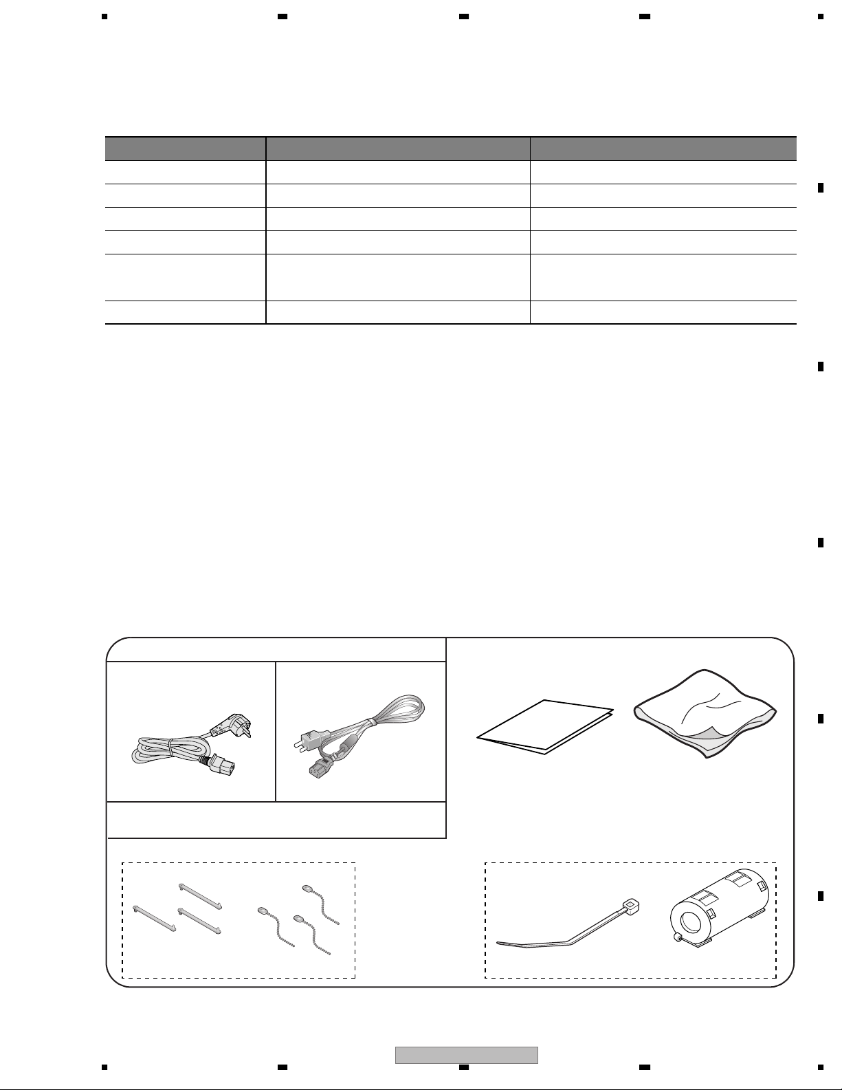
Accessories
Power cord (2 m)
For PDP-506PE For PDP-506PU
Warranty card
(ADG1214) (ADG1215)
Only the power cord that is appropriate in your country or region
is supplied.
Binder Assy (AEC1908) Ferrite Core (ATX1039)(PDP-506PE only)
Speed clamp x 3 Bead band x 3
Cable tie
Cleaning cloth
(AED1285)
D
E
Ferrite core
F
56
PDP-506PE
7
7
8
Page 8
1234
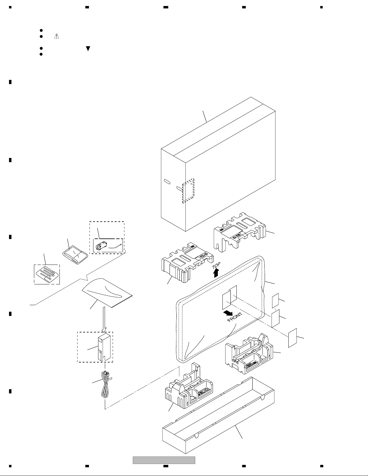
2. EXPLODED VIEWS AND PARTS LIST
NOTES:
Parts marked by "NSP" are generally unavailable because they are not in our Master Spare Parts List.
The mark found on some component parts indicates the importance of the safety factor of the part.
A
Therefore, when replacing, be sure to use parts of identical designation.
Screws adjacent to mark on product are used for disassembly.
For the applying amount of lubricants or glue, follow the instructions in this manual.
(In the case of no amount instructions, apply as you think it appropriate.)
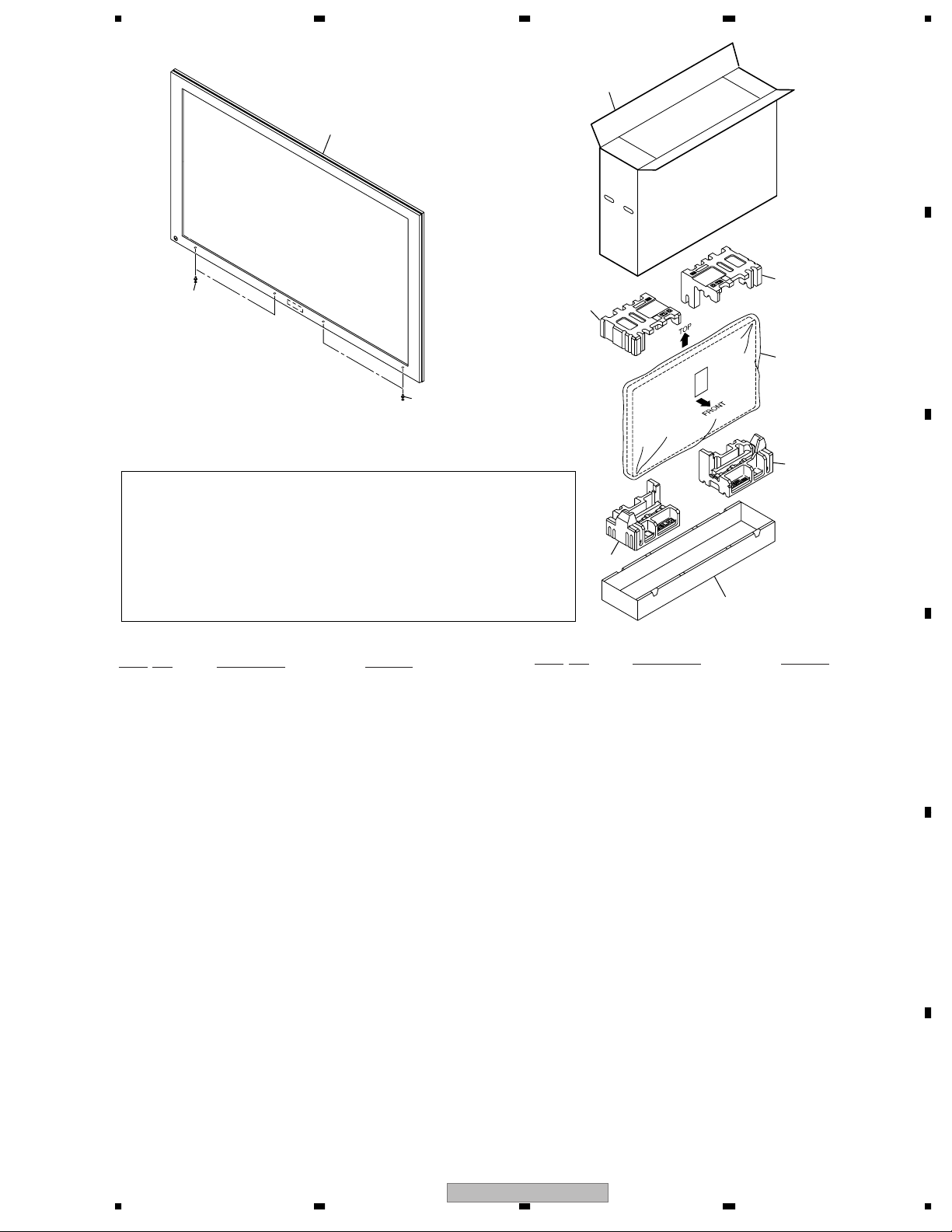
2.1 PACKING SECTION
B
C
14
PDP-506PEonly
PDP-506PE only
7
3
2
D
8
4
PDP-506PE
only
E
12
1
9
15
6
5
16
11
10
F
13
8
1234
PDP-506PE
Page 9
>
>
>
>
5678
(1) PACKING SECTION PARTS LIST
No. Description Part No.
Mark
1Power Cord See Contrast table (2)
2 Binder Assy AEC1908
3 Cleaning Cloth AED1285
4Polyethylene Bag S See Contrast table (2)
NSP 5 Catalogue Bag See Contrast table (2)
NSP 6 Warranty card See Contrast table (2)
7Ferrite Core See Contrast table (2)
8Pad (50T-L) See Contrast table (2)
9Pad (50T-R) See Contrast table (2)
10 Pad (50B-L) See Contrast table (2)
A
11 Pad (50B-R) See Contrast table (2)
12 Power Cord Case See Contrast table (2)
13 Under Carton See Contrast table (2)
14 Upper Carton See Contrast table (2)
15 Mirror Mat See Contrast table (2)
16 Caution Card See Contrast table (2)
(2) CONTRAST TABLE
PDP-506PE/WYVI and PDP-506PU/KUCXC are constructed the same except for the following:
Mark No. Symbol and Description PDP-506PE/WYVI PDP-506PU/KUCXC
1Power Cord ADG1214 ADG1215
4Polyethylene Bag S AHG1338 AHG1348
NSP 5 Catalogue Bag AHG1340 AHG1347
NSP 6 Warranty Card ARY1114 ARY1145
7Ferrite Core ATX1039 Not used
8Pad (50T-L) AHA2427 AHA2459
9Pad (50T-R) AHA2428 AHA2460
10 Pad (50B-L) AHA2429 AHA2461
11 Pad (50B-R) AHA2430 AHA2462
12 Power Cord Case AHC1073 Not used
B
C
D
13 Under Carton (50) AHD3344 Not used
13 Under Carton (506PU) Not used AHD3379
14 Upper Carton (506PE) AHD3345 Not used
14 Upper Carton (506PU) Not used AHD3383
15 Mirror Mat AHG1284 AHG1352
16 Caution Card ARM1232 ARM1239
PDP-506PE
56
7
8
E
F
9
Page 10
1234
2.2 REAR SECTION
A
4
11
B
16
C
16
3
15
15
15
7
6
PDP-506PE
8
only
15
15
15
4
16
11
15
2
To Power Switch
D
5
E
15
12
13
15
14
15
1
5
Refer to
F
10
1234
"2.3 FRONT SECTION".
PDP-506PE
Page 11
>
5678
(1) REAR SECTION PARTS LIST
No. Description Part No.
Mark
1AC Inlet AKP1274
2 Control Plate AND1185
3 Rear Case (506) ANE1639
4 Inner Grip Assy AMR3434
5AC Cushion AEC2035
NSP 6 Model Label See Contrast table (2)
7 Caution Label See Contrast table (2)
8AC Label PE See Contrast table (2)
9• • • • •
10 • • • • •
A
11 Screw (3 x 40P) ABA1332
12 Hexagon Head Screw BBA1051
13 Screw PMZ26P060FTB
14 Screw BPZ30P080FTB
15 Screw AMZ30P060FTB
16 Screw TBZ40P080FTB
(2) CONTRAST TABLE
PDP-506PE/WYVI and PDP-506PU/KUCXC are constructed the same except for the following:
Mark No. Symbol and Description PDP-506PE/WYVI PDP-506PU/KUCXC
NSP 6 Model Label (506PE) AAL2661 Not used
NSP 6 Model Label (506PU) Not used AAL2679
7 Caution Label AAX3117 AAX3075
8AC Label PE AAX3194 Not used
B
C
D
56
PDP-506PE
E
F
11
7
8
Page 12
1234
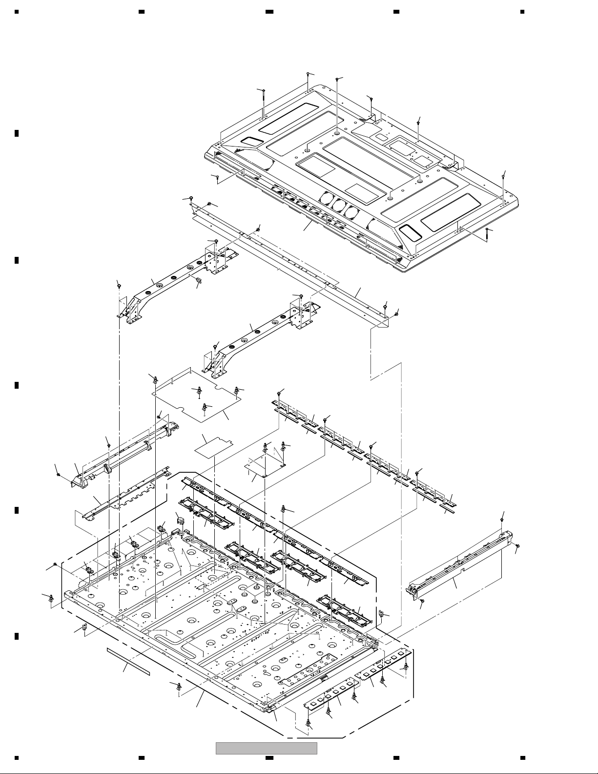
2.3 FRONT SECTION
A
B
Refer to
"2.4 CHASSIS SECTION (1/2)",
C
D
PDP-506PE
only
E
7
7
5
4
9
2
8
10
6
3
7
1
7
8
10
F
12
1234
PDP-506PE
Page 13
5678
(1) FRONT SECTION PARTS LIST
No. Description Part No.
Mark
1Front Case Assy (506PE) AMB2861
2 Corner Cushion AEB1416
3 Pioneer Name Plate AAM1098
4Power Button AAD4133
5 Coil Spring ABH1120
6 Blind Cushion AEB1415
7 Insulation Sheet A AED1283
8 Insulation Sheet B AED1284
9Power Display Label (506) See Contrast table (2)
10 Screw Rivet AEC1877
(2) CONTRAST TABLE
PDP-506PE/WYVI and PDP-506PU/KUCXC are constructed the same except for the following:
Mark No. Symbol and Description PDP-506PE/WYVI PDP-506PU/KUCXC
9Power Display Label (506) AAX3217 Not used
A
B
C
D
E
56
PDP-506PE
F
13
7
8
Page 14
1234
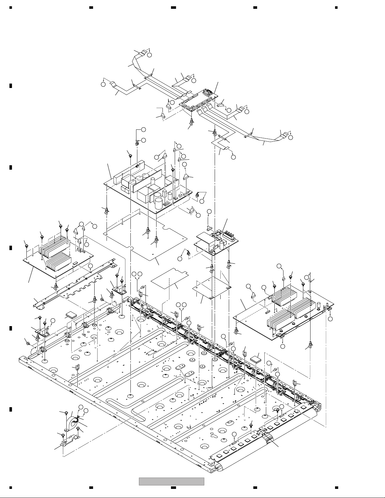
2.4 CHASSIS SECTION (1/2)
A
To HD DIGITAL
CN3003
19
17
1
18
16
22
B
8
22
14
22
7
9
19
17
22
C
2
From POWER SUPPLY
P3
1
17
23
From AC Inlet
21
12
23
23
D
4
3
Refer to
"2.5 CHASSIS SECTION (2/2)".
11
17
6
To HD DIGITAL
14
E
20
17
CN3003
2
5
10
13
17
10
11
23
20
F
14
1234
PDP-506PE
17
12
Page 15

5678
CHASSIS SECTION (1/2) PARTS LIST
No. Description Part No.
Mark
1 HD LED Assy AWW1029
2 HD IR Assy AWW1030
3Power Switch (S1) ASG1092
4 Housing Wire (50)(J103) ADX3112
5Front Chassis VL (50) AMA1014
6Front Chassis VR (50) AMA1015
7 Sub Frame L Assy (506) ANA1860
8 Sub Frame R Assy (506) ANA1861
9Front Chassis H Assy (50) ANA1883
10 Panel Holder H (50) ANG2769
>
A
11 Panel Holder V1 (50) ANG2770
12 Panel Holder V2 (50) ANG2771
13 Cushion AEB1424
14 Wire Saddle AEC1745
15 • • • • •
16 Nyron Rivet AEC1671
17 Screw ABZ30P080FTC
18 Screw AMZ30P060FTB
19 Screw APZ30P080FTB
20 Screw BBZ30P060FTC
21 Screw BPZ30P080FTB
22 Screw TBZ40P080FTB
23 Screw VBB30P080FNI
B
C
D
56
PDP-506PE
E
F
15
7
8
Page 16
1234
2.5 CHASSIS SECTION (2/2)
A
E
15
B
7
9
A
14
31
To HD LED CN1671
HD IR CN1681
19
1
To
Power Switch
2
41
31
24
9
13
B
N
32
R
25
41
O
26
N
J
32
10
5
18
9
Q
C
12
31
31
11
F
9
D
21
L
C
40
41
41
40
17
32
J
R
32
G
32
23
Q
K
6
36
M
37
R R
30
35
B
36
32
40
41
3
R R
34
36
A
E
1
D
27
32
40
32
41
40
33
G
2
32
40
E
36
30
K
O
41
41
16
41
F
P
4
I
O
32
36
C
33
H
32
P
D
36
I
40
41
39
L
8
M
29
40
22
41
H
F
16
28
PDP-506PE
20
1234
Page 17
5678
(1) CHASSIS SECTION (2/2) PARTS LIST
No. Description Part No.
Mark
1 50 X DRIVE Assy See Contrast table (2)
2 SUS CLAMP 1 Assy AWW1022
3 SUS CLAMP 2 Assy AWW1023
4 50 Y DRIVE Assy See Contrast table (2)
5 HD DIGITAL Assy AWW1028
>
No. Description Part No.
Mark
21 14P Housing Wire (J104) ADX3158
22 3P Housing Wire (J105) ADX3159
23 9P Housing Wire (J101) ADX3186
24 8P Housing Wire (J102) ADX3187
25 5P Housing Wire (J106) ADX3188
A
6 HD AUDIO Assy AWV2203
7POWER SUPPLY Unit AXY1112
8 Ring Core with Case ATX1042
9Ferrite Core ATX1048
10 Flexible Cable (J201) ADD1293
11 Flexible Cable (J202) ADD1294
12 Flexible Cable (J203) ADD1295
13 Flexible Cable (J204) ADD1296
14 Flexible Cable (J205) ADD1297
15 Flexible Cable (J206) ADD1298
16 4P Housing Wire (J108) ADX3117
17 6P Housing Wire (J109) See Contrast table (2)
18 12P Housing Wire (J110) See Contrast table (2)
19 6P Housing Wire (J111) ADX3120
20 3P Housing Wire (J113) See Contrast table (2)
26 6P Housing Wire (J107) ADX3189
27 Conductive Plate XA ANG2776
28 FC Stay ANG2815
29 Binder AEC-093
NSP 30 PCB Spacer AEC1188
31 Flat Clamp AEC1879
32 PCB Spacer AEC1941
33 Drive Silicone Sheet AEH1095
34 Power Supply Insulation Sheet AMR3447
35 Audio Insulation Sheet AMR3469
36 Wire Saddle AEC1745
NSP 37 Address Sheet AMR3491
38 • • • • •
39 Screw ABA1324
40 Screw PMB30P060FTC
41 Screw VBB30P080FNI
B
C
(2) CONTRAST TABLE
PDP-506PE/WYVI and PDP-506PU/KUCXC are constructed the same except for the following:
Mark No. Symbol and Description PDP-506PE/WYVI PDP-506PU/KUCXC
1 50 X DRIVE Assy AWW1075 AWW1020 or AWW1075
4 50 Y DRIVE Assy AWV2258 AWV2210 or AWV2258
17 6P Housing Wire (J109) ADX3118 ADX3132
18 12P Housing Wire (J110) ADX3119 ADX3133
20 3P Housing Wire (J113) ADX3122 ADX3136
D
E
F
56
PDP-506PE
17
7
8
Page 18
1234
2.6 PDP SERVICE ASSY 506P (AWU1134)
A
29
34
B
34
C
16
32
21
30
31
34
34
15
34
34
37
(for transport)
31
31
17
32
31
34
29
30
23
23
30
35
D
14
30
18
6
6
6
E
33
23
21
2
8
6
23
26
7
23
24
25
2
12
9
12
11
20
10
11
23
7
20
7
2
9
12
10
11
10
2
7
21
12
9
9
11
10
13
30
35
30
19
F
18
1234
23
5
1
38
4
5
5
PDP-506PE
5
5
3
Page 19
5678
• Front Section • Packing Section
43
(for transport)
36
22
38
A
39
B
28
Note when replacing with the PDP Service Assy 506P
The Power Switch (S1), HD LED Assy, and HD IR Assy are not
included in the PDP Service Assy 506P. Before replacement with the
PDP Service Assy 506P, the following components of the Service Assy
must be temporarily detached to attach the above-mentioned parts
(parts from the original unit or newly purchased):
• Front Chassis H Assy (50) (ANA1883)
• Front Chassis VL (50) (AMA1014)
• Front Chassis VR (50) (AMA1015)
PDP SERVICE ASSY 506P (AWU1134) PARTS LIST
No. Description Part No.
Mark
NSP 1 Panel Chassis (506) Assy AWU1143
NSP 2 50 ADDRESS Assy AWV2208
NSP 3 50 SCAN A Assy AWW1026
NSP 4 50 SCAN B Assy AWW1027
5 PCB Spacer AEC1944
6 Conductive Plate Holder AMR3446
7 ADDRESS Holder Assy (50) AMR3454
8Tube Cover AMR3445
9 Address Heatsink (50) ANH1635
10 Address Silicone A AEH1093
11 Address Silicone B AEH1094
12 Screw BBB30P120FNI
13 Front Chassis VL (50) AMA1014
14 Front Chassis VR (50) AMA1015
15 Sub Frame L Assy (506) ANA1860
16 Sub Frame R Assy (506) ANA1861
17 Front Chassis H Assy (50) ANA1883
18 Conductive Plate XA ANG2776
19 Cushion AEB1424
NSP 20 PCB Spacer AEC1188
21 Wire Saddle AEC1745
22 Screw Rivet AEC1877
56
PDP-506PE
41
22
40
42
No. Description Part No.
Mark
23 PCB Spacer AEC1941
24 Power Supply Insulation Sheet AMR3447
25 Audio Insulation Sheet AMR3469
NSP 26 Address Sheet AMR3491
NSP 27 Chassis Assy (50) ANA1830
28 Protect Sheet AHG1331
29 Screw (3 x 40P) ABA1332
30 Screw ABZ30P080FTC
31 Screw AMZ30P060FTB
32 Screw APZ30P080FTB
33 Screw PMB30P060FTC
34 Screw TBZ40P080FTB
35 Screw VBB30P080FNI
NSP 36 Front Case Assy (506 serivice) AMB2889
(for transport)
NSP 37 Rear Case (506) ANE1639
(for transport)
38 Pad (50T-L) AHA2427
39 Pad (50T-R) AHA2428
40 Pad (50B-L) AHA2429
41 Pad (50B-R) AHA2430
42 Under Carton AHA3344
43 Upper Carton (506 S.V.C) AHA3430
7
8
C
D
E
F
19
Page 20
1234
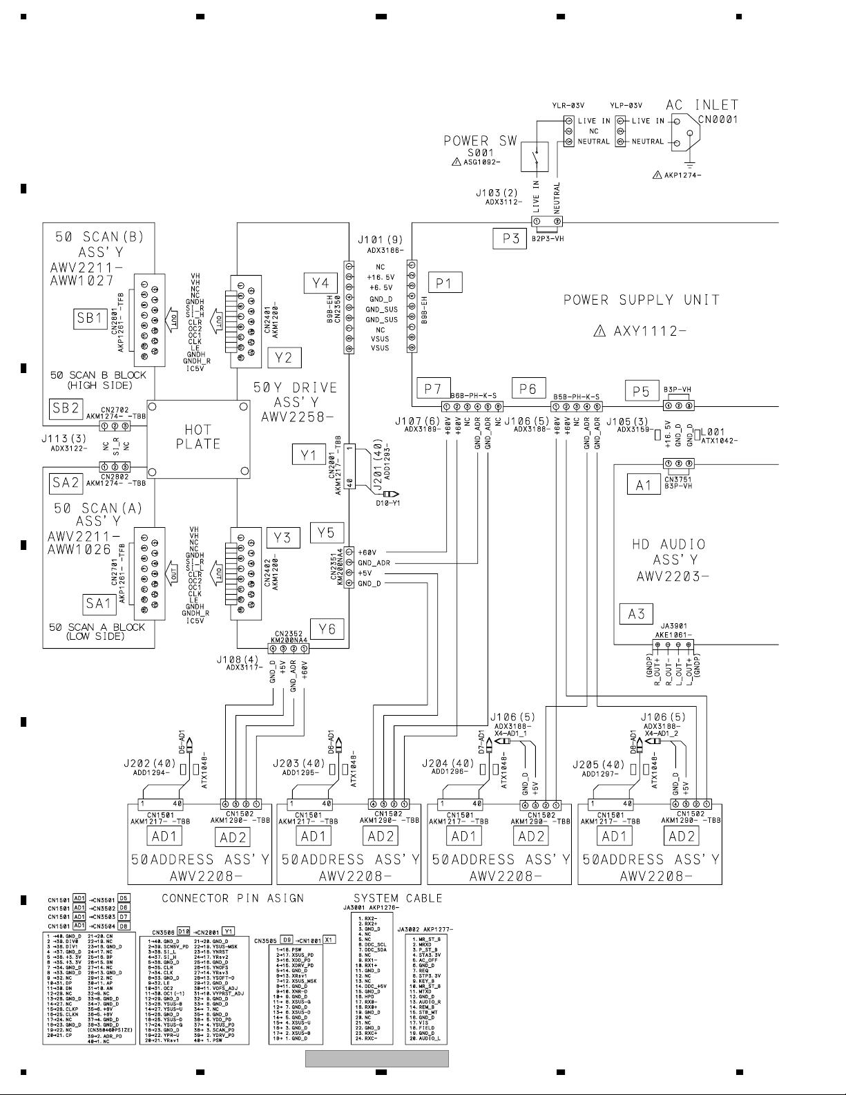
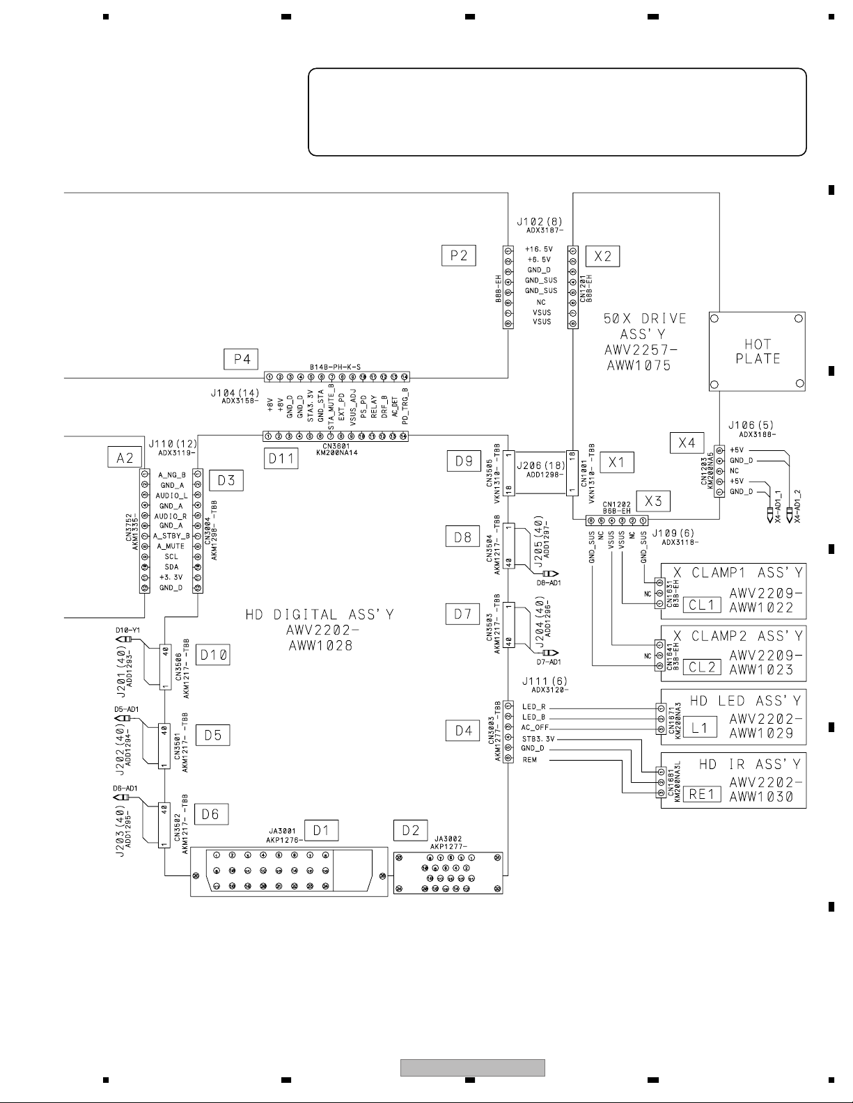
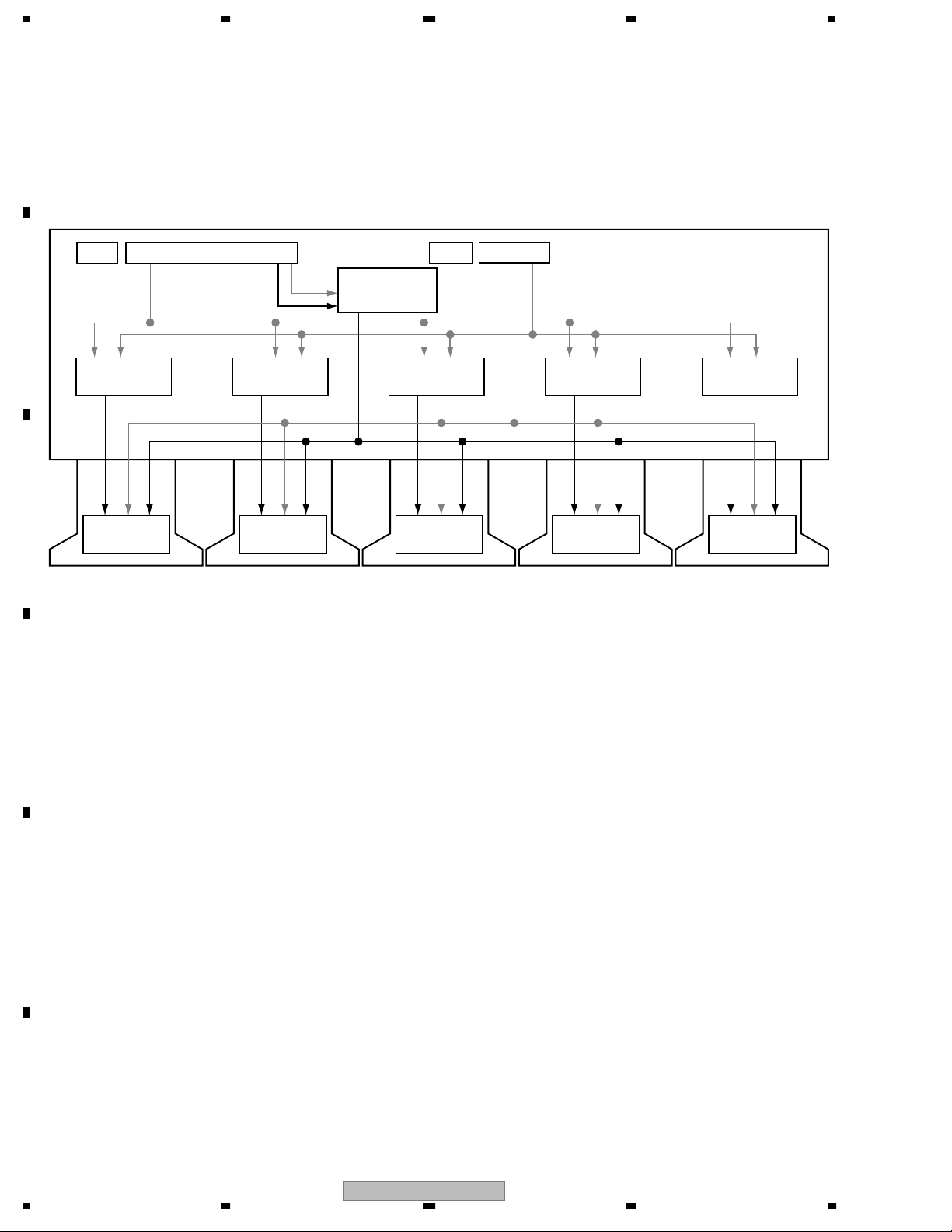
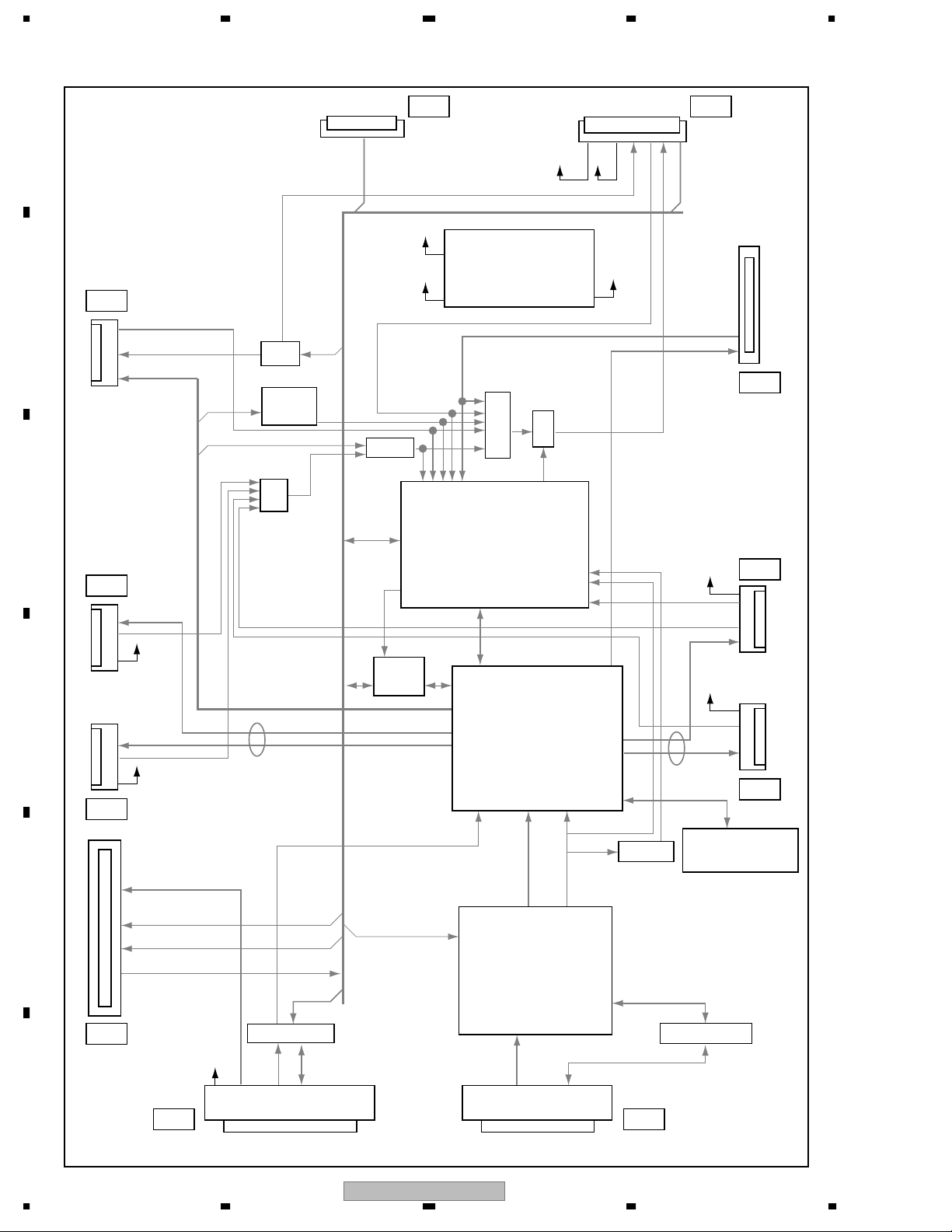
3. BLOCK DIAGRAM AND SCHEMATIC DIAGRAM
3.1 OVERALL CONNECTION DIAGRAM
A
B
C
D
E
F
20
1234
PDP-506PE
Page 21
5678
÷
When ordering service parts, be sure to refer to "EXPLODED VIEWS and PARTS
LIST" or "PCB PARTS LIST".
÷
The > mark found on some component parts indicates the importance of the safety
A
factor of the part. Therefore, when replacing, be sure to use parts of identical
designation.
B
C
D
E
56
PDP-506PE
F
21
7
8
Page 22
1234
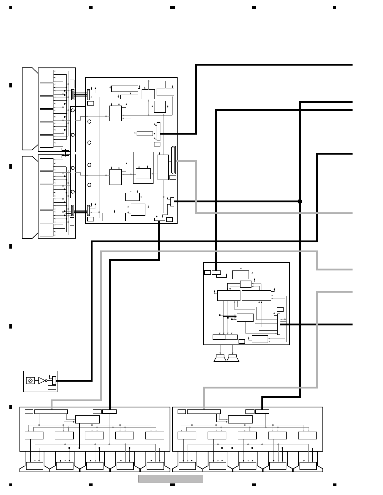
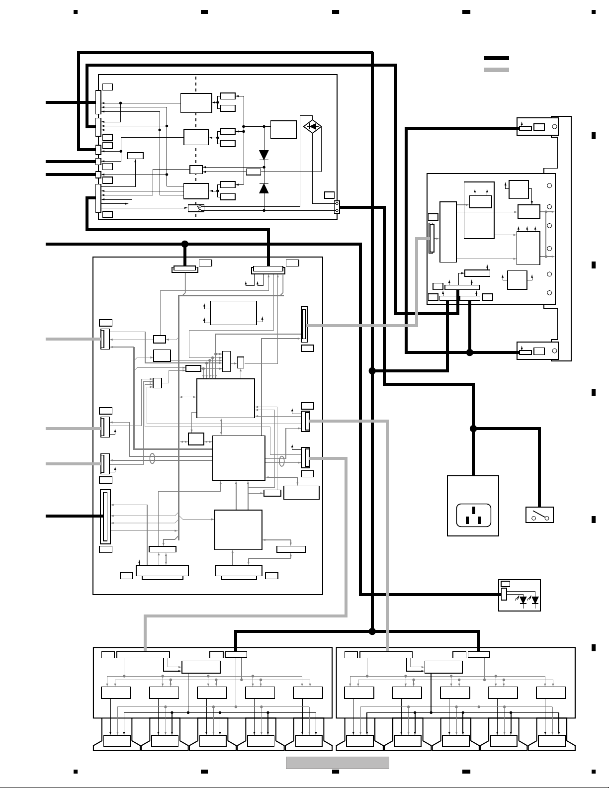
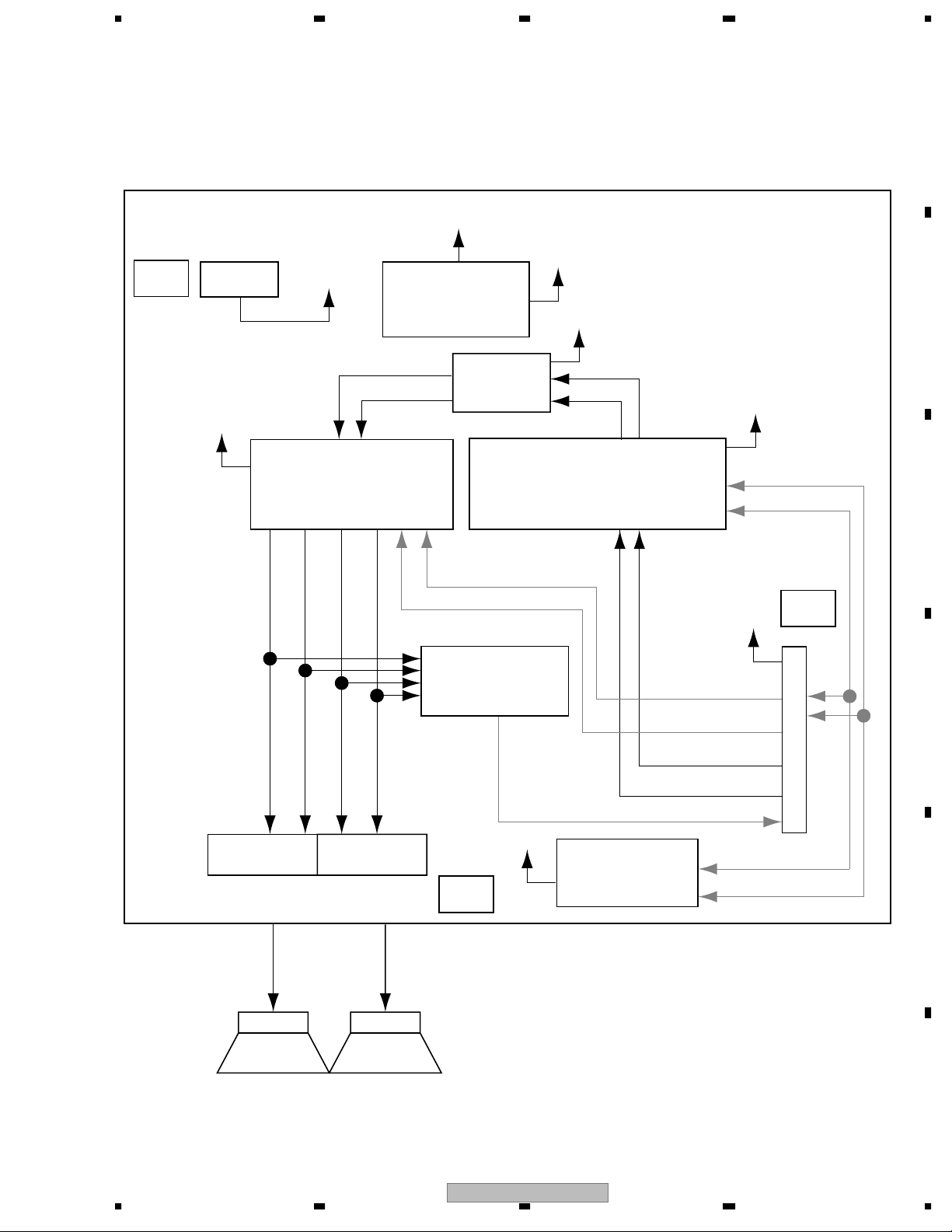
3.2 OVERALL BLOCK DIAGRAM
A
50 SCAN B ASSY
(UPPER)
Scan Signal
VH
IC2801
IC5V
Scan IC
PSUS
IC2802
Scan IC
IC2803
Scan IC
IC2804
Scan IC
B
C
IC2805
Scan IC
IC2806
Scan IC
CN2802
CN2702
IC2701
Scan IC
IC2702
Scan IC
IC2703
Scan IC
IC2704
Scan IC
IC2705
Scan IC
IC2706
Scan IC
Serial Data
PSUS
IC5V
VH
Scan Signal
50 SCAN A ASSY
(LOWER)
D
50 Y DRIVE ASSY
PSUS
PSUS
VH
IC5V
IC5V
VH VSUS
Vprst
+5V +16.5V
+5V
Photo Coupler
SB1
SA1
VH
Y2
Y3
VH DC/DC Conv.
Vprst Reg.
VSUS
IC2252
Mask
Mod.
VSUS
+16.5V
IC2253
Mask
Mod.
IC5V
IC5V
VF
Block
SUSOUT
Soft-D
Block
Vprst
+5V
Regulator
Resonance
Block
+5V
IC2101
DK Mod.
+16.5V
IC5V/VF
DC/DC
Conv.
Scan Signal
+ Reset
Block
VOFS
+16.5V
+16.5V
+16.5V
VSUS
+6.5V
+5V
VOFS
DC/DC
Conv.
Y4
+5V
Logic
Block
Offset
Block
+16.5V
Drive Signal
+5V
Y6
VOFS
Y1
Y5
60V
A1
+16.5V
+16.5V
IC3751
Power Amp IC
R_OUT +
R_OUT –
L_OUT +
Left
Right
SP TERMINAL
HD AUDIO ASSY
+16.5V
+9.0V
IC3752
Regulator
+9.0V
Buffer
IC3753
WOW + Volume IC
DC Detect
L_OUT –
Block
+3.3V
A3
A_STBY_B
IC3754
EEP ROM
A_Mute
R_Audio
L_Audio
A_NG_B
+9.0V
+3.3V
SCL
SDA
SDA
SCL
A2
E
HD IR ASSY
IR Receive unit
STB3.3V
U1681
RE1
CN1501
AD1 AD2
AN/P BN/P
V+8V
CN/P DN/P CLKN/P
Resonance
Block
V+ADR5
Resonance
Block
V+ADR4
F
IC1555
Driver IC
IC1554
Driver IC
22
1234
V+3V
IC1501
LVDS Receiver
Resonance
Block
V+ADR3
IC1553
Driver IC
SPEAKERS
CN1502
V+5V
(PEE002A-K) (PEE002A-K)
CLK/LE/HBLK/LBLK
R/G/B
50 ADDRESS
V+60V
ASSY
Resonance
Block
V+ADR2
IC1552
Driver IC
Resonance
Block
V+ADR1
IC1551
Driver IC
AD1 AD2
Resonance
V+8V
Block
V+ADR5
IC1555
Driver IC
CN1501
AN/P BN/P
CN/P DN/P CLKN/P
Resonance
Driver IC
Block
V+ADR4
IC1554
V+3V
IC1501
LVDS Receiver
Resonance
Block
V+ADR3
IC1553
Driver IC
CN1502
CLK/LE/HBLK/LBLK
R/G/B
PDP-506PE
50 ADDRESS
V+60VV+5V
ASSY
Resonance
Block
V+ADR2
IC1552
Driver IC
Resonance
Block
V+ADR1
IC1551
Driver IC
Page 23
5678
P1
P2
P7
+60V
P6
+16.5V
P5
VSUS_ADJ
+8V
STA3.3V
RELAY
P4
D10
Vofs_ADJ,VYPRST_ADJ
SCAN
YSUS
D5
V+8V
V+8V
D6
AUDIO L
AUDIO R
SCL, SDA
A_MUTE,A_STBY_B
A_NG
D3
SECONDARY PRIMARY
VSUS
+16.5V
+6.5V
VSUS_CONT
IC202
PS_PD
EXT_PD
LED_R
LED_B
REM
SCAN_PD
YDRV_PD
YSUS_PD
YDD_PD
SCN5V_PD
V+3V STB
D2 D1
DAC
Pulse
Width
OR
LVDS
Bus Buffer
SCL,
SCA
ADR_PD1
REM
STB_MT
HD DIGITAL ASSY
Switching
RY102
Q703
Q704
Switching
Switching
Q901
Q902
Switching
Switching
Q501
Q502
Switching
IC101
Switching
T702
T902
T101
T502
D4 D11
V+3V ACT
Vsus_ADJ
V+3V_D
DC-DC Converter
V+1V_D
PS_PWDN
SQ_PD
Mask
UART
SW
SCL, SDA
Module
(AXY1116)
OR
IC3151
(M30620FCPGP)
Module Ucom
IC3401
(PEG122C-K)
Sequence
Processor
FIELD
IC3001
TMDS Receiver
TMDS
DVI CONNECTORMDR CONNECTOR
PD
PD_MUTE
VD
HD
DCLK, DERA, GA, BA
POWER SUPPLY
UNIT
+390V
PFC Q101
Q102
Q103
D109
D107, D108
NEUTRAL
V+8V
DDC
XSUS
PSIZE
H DET
RELAY,
PD_TRIGGER
AC_DET,
DRF
XSUSTN_PD
XDD_CNV_PD
XDRIVE_PD
V+8V
V+8V
LVDS
IC3301
Flash Memory
Bus Buffer
D9
D8
D7
V+8V
D103
LIVE
: Wire haerness
: FFC
A
SUS CLAMP 1
ASSY
VSUS
CL1
50 X DRIVE ASSY
+16.5V
VRN
+5V
Logic
Block
+5V
Drive Signal
+6.5V
+16.5V
IC1101
DK Mod.
Resonance
Block
Regulator
VSUS
VSUS
SUS OUT
+5V
+16.5V VF
P3
X1
+16.5V
X2
X4 X3
DC/DC
Conv.
+16.5V
15V
DC/DC
Conv.
– Reset
Block
+5V
IC1202
Mask
Mod.
VRN
B
VSUS
PSUS
C
VSUS
CL2
SUS CLAMP 2
ASSY
D
POWER SW
AC INLET
HD LED ASSY
L1
E
V+8V
Block
V+ADR5
IC1555
Driver IC
CN1501
AN/P BN/P
CN/P DN/P CLKN/P
Resonance
Driver IC
Block
V+ADR4
IC1554
V+3V
IC1501
LVDS Receiver
Resonance
Block
V+ADR3
IC1553
Driver IC
CLK/LE/HBLK/LBLK
AD1 AD2
Resonance
56
CN1502
(PEE002A-K) (PEE002A-K)
R/G/B
50 ADDRESS
V+60VV+5V
ASSY
Resonance
Block
V+ADR2
IC1552
Driver IC
Resonance
Block
V+ADR1
IC1551
Driver IC
AD1 AD2
V+8V
Resonance
Block
V+ADR5
IC1555
Driver IC
CN1501
AN/P BN/P
CN/P DN/P CLKN/P
Resonance
Driver IC
Block
V+ADR4
IC1554
V+3V
LVDS Receiver
IC1501
Resonance
Block
IC1553
Driver IC
CN1502
V+ADR3
CLK/LE/HBLK/LBLK
R/G/B
PDP-506PE
7
50 ADDRESS
V+60VV+5V
ASSY
Resonance
Block
V+ADR2
IC1552
Driver IC
Resonance
8
Block
V+ADR1
IC1551
Driver IC
F
23
Page 24
1234
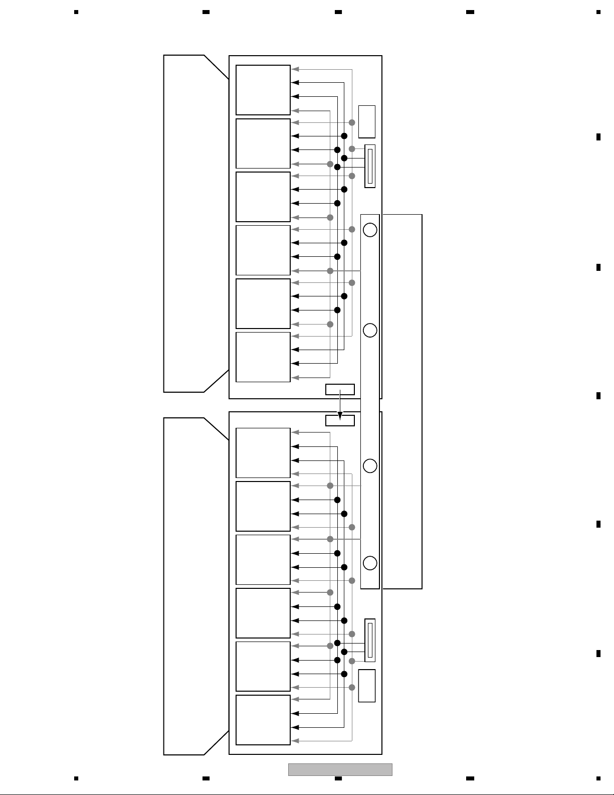
3.3 50 ADDRESS ASSY
A
AD1 AD2
V+8V
B
Resonance
Block
V+ADR5
C
IC1555
Driver IC
CN1501
AN/P BN/P
CN/P DN/P CLKN/P
Resonance
Block
IC1554
Driver IC
V+3V
V+ADR4
IC1501
(PEE002A-K)
LVDS Receiver
Resonance
Block
V+ADR3
IC1553
Driver IC
CN1502
V+60VV+5V
Resonance
CLK/LE/HBLK/LBLK
R/G/B
Block
V+ADR2
IC1552
Driver IC
Resonance
Block
V+ADR1
IC1551
Driver IC
D
E
F
24
PDP-506PE
1234
Page 25
5678
3.4 50 SCAN A and B ASSYS
IC2801
Scan IC
IC2802
Scan IC
IC2803
Scan IC
IC2804
Scan IC
IC2805
Scan IC
IC2806
Scan IC
Scan Signal
VH
IC5V
PSUS
50 SCAN B ASSY
(UPPER)
SB1
A
B
C
IC2701
Scan IC
IC2702
Scan IC
IC2703
Scan IC
IC2704
Scan IC
IC2705
Scan IC
CN2802
Serial Data
CN2702
D
E
SA1
IC2706
Scan IC
PSUS
IC5V
VH
Scan Signal
50 SCAN A ASSY
(LOWER)
PDP-506PE
56
F
25
7
8
Page 26
1234
3.5 50 X DRIVE, SUS CLAMP 1 and SUS CLAMP 2 ASSYS
A
ASSY
SUS CLAMP 1
VSUS
CL1
B
50 X DRIVE ASSY
+16.5V
+16.5V
DK Mod.
C
+5V
IC1101
VRN
DC/DC
Conv.
VRN
– Reset
Block
X1
Logic
Block
Resonance
Block
+16.5V
SUS OUT
+5V
VSUS
IC1202
Mask
Mod.
+6.5V
Drive Signal
Regulator
VSUS
+5V
PSUS
+16.5V VF
15V
DC/DC
Conv.
D
+16.5V
X2
+5V
VSUS
X4 X3
E
SUS CLAMP 2
F
ASSY
VSUS
CL2
26
PDP-506PE
1234
Page 27
5678
3.6 50 Y DRIVE ASSY
VH
IC5V
VH VSUS
VH DC/DC Conv.
Vprst
Vprst Reg.
Vprst
+ Reset
Block
Offset
Block
A
VOFS
Y2
PSUS
+5V +16.5V
IC2252
Mask
Mod.
+16.5V
+5V
VSUS
VSUS
+5V
SUSOUT
Regulator
Resonance
Block
+5V
+16.5V
VOFS
VSUS
+6.5V
+16.5V
VOFS
DC/DC
Conv.
Y4
+5V
+16.5V
B
Drive Signal
C
D
Logic
Block
PSUS
VH
Y3
IC5V
IC2253
Mask
Mod.
IC5V
Photo Coupler
Block
IC5V
VF
+16.5V
Soft-D
Block
IC5V/VF
DC/DC
Conv.
Scan Signal
PDP-506PE
56
IC2101
DK Mod.
+16.5V
7
+5V
+5V
60V
Y6
Y1
E
Y5
F
27
8
Page 28
1234
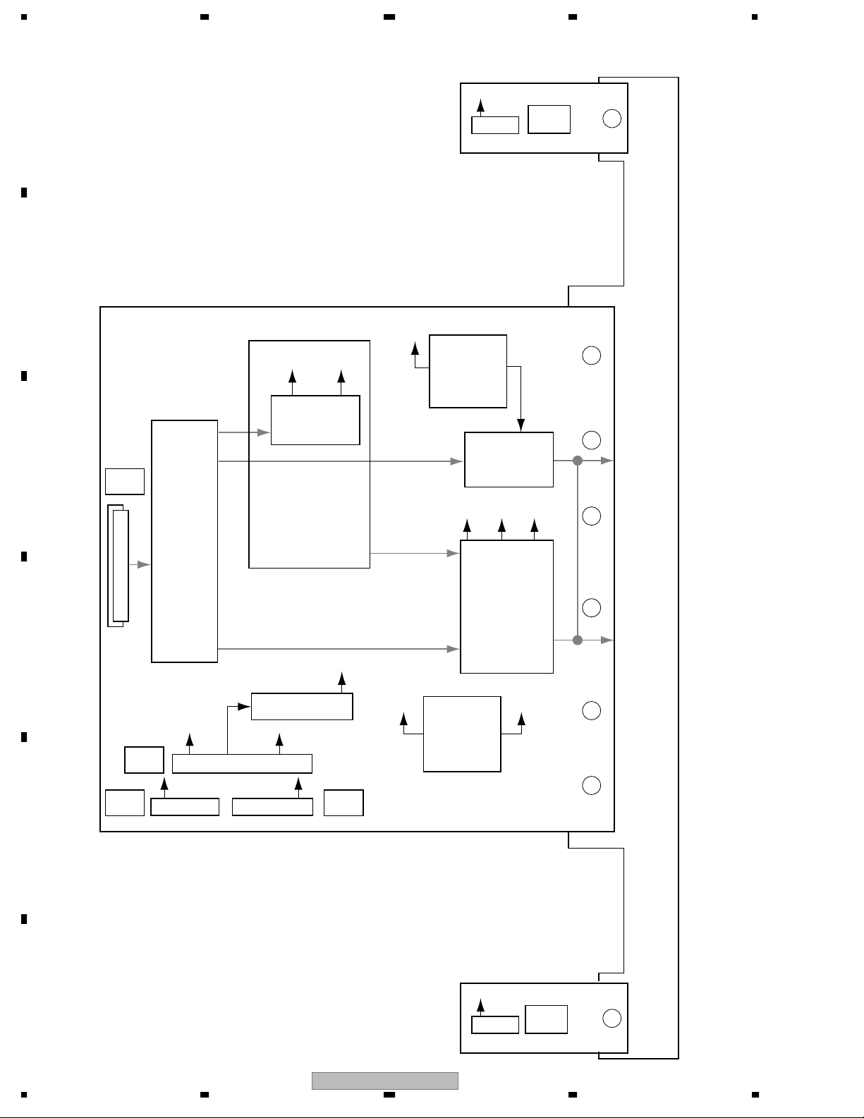
3.7 HD DIGITAL ASSY
A
LED_R
LED_B
REM
SCAN_PD
YDRV_PD
B
C
D10
YSUS_PD
YDD_PD
SCN5V_PD
Vofs_ADJ,VYPRST_ADJ
SCAN
YSUS
DAC
Pulse
Width
OR
SCL,
SCA
ADR_PD1
D4 D11
V+8V
V+8V
XSUS
PD
PD_MUTE
V+3V_D
V+1V_D
PS_PWDN
SQ_PD
Mask
V+3V ACT
Vsus_ADJ
DC-DC Converter
Module
(AXY1116)
OR
IC3151
(M30620FCPGP)
RELAY,
PD_TRIGGER
AC_DET,
DRF
XSUSTN_PD
XDD_CNV_PD
XDRIVE_PD
D9
Module Ucom
D5
V+8V
UART
SW
D
V+8V
LVDS
IC3401
(PEG122C-K)
Sequence Processor
PSIZE
LVDS
V+8V
V+8V
D8
D7
D6
FIELD
AUDIO L
AUDIO R
E
SCL, SDA
A_MUTE,A_STBY_B
A_NG
SCL, SDA
RA, GA, BA
IC3001
TMDS Receiver
VD
HD
DCLK, DE
H DET
IC3301
Flash Memory
D3
V+3V STB
F
28
D2
1234
Bus Buffer
REM
STB_MT
PDP-506PE
TMDS
DVI CONNECTORMDR CONNECTOR
DDC
Bus Buffer
D1
Page 29
5678
3.8 HD AUDIO ASSY
A1
+16.5V
+16.5V
+16.5V
IC3752
Regulator
Buffer
+9.0V
+9.0V
+9.0V
A
B
R_OUT +
Right
IC3751
Power Amp IC
R_OUT –
L_OUT +
SP TERMINAL
L_OUT –
Left
DC Detect
Block
A3
WOW + Volume IC
+3.3V
IC3753
EEP ROM
IC3754
SCL
SDA
+3.3V
A_Mute
A_STBY_B
R_Audio
L_Audio
A_NG_B
SDA
SCL
C
A2
D
E
SPEAKERS
PDP-506PE
56
F
29
7
8
Page 30

1234
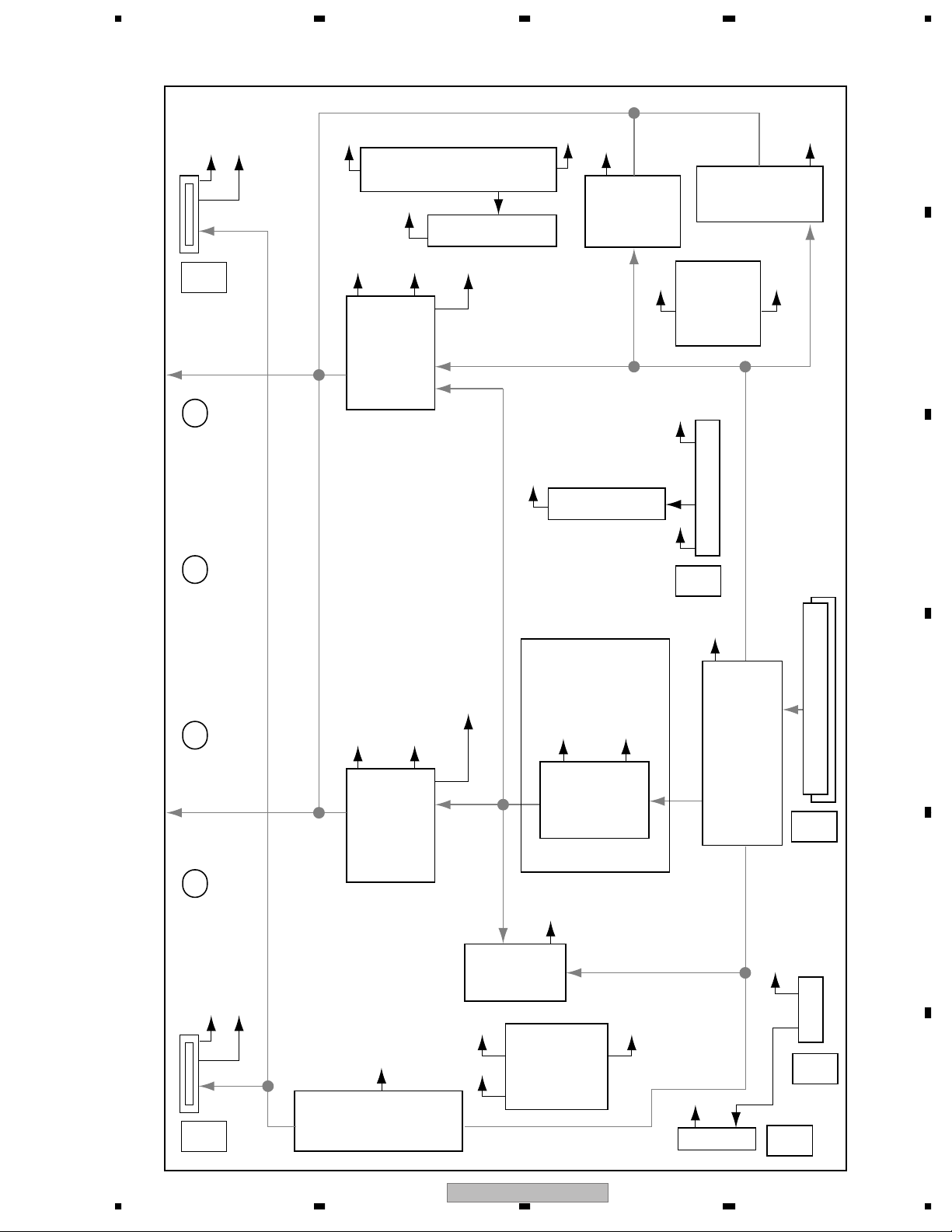
3.9 POWER SUPPLY UNIT
A
SECONDARY PRIMARY
P1
B
VSUS
+16.5V
+6.5V
P2
P7
C
+60V
VSUS_CONT
IC202
T702
T902
Switching
Q703
Q704
Switching
Switching
Q901
Q902
Switching
+390V
PFC Q101
Q102
Q103
D109
D103
P6
+16.5V
P5
VSUS_ADJ
+8V
STA3.3V
PS_PD
RELAY
EXT_PD
P4
D
E
T502
T101
RY102
Switching
Q501
Q502
Switching
IC101
Switching
D107, D108
P3
NEUTRAL
LIVE
F
30
1234
PDP-506PE
Page 31

5678
3.10 WAVEFORMS
Note : The encircled numbers denote measuring point in the schematic diagram.
Refer to service manual (ARP3268).
50 ADDRESS ASSY
50 ADDRESS RESONANCE BLOCK
Control signal of resonance circuit (1 field)
1
Input : VIDEO 60Hz
Signal : Color-bar (MKSS17)
CH1 : ADR_B2
1-1
V : 1V/div H : 2msec/div
CH2 : ADR_U2
1-2
V : 1V/div H : 2msec/div
CH3 : ADR_D2
1-3
V : 1V/div H : 2msec/div
Control signal of resonance circuit (2 FS)
1
Input : VIDEO 60Hz
Signal : Color-bar (MKSS17)
CH1 : ADR_B2
1-1
V : 1V/div H : 2msec/div
CH2 : ADR_U2
1-2
V : 1V/div H : 2msec/div
CH3 : ADR_D2
1-3
V : 1V/div H : 2msec/div
1-1
1-2
1-3
1-1
50 ADDRESS LOGIC BLOCK TCP LOGIC
VADR (1 field)
2
Input : VIDEO 60Hz
Signal : Color-bar (MKSS17)
CH2 : IC1555-pin 3 (VDD2)
V : 10V/div H : 2msec/div
VADR (1 field)
2
Input : VIDEO 60Hz
Signal : Checkered pattern of Black-White (MKSS13)
CH2 : IC1555-pin 3 (VDD2)
V : 10V/div H : 2msec/div
Incoming signal of TCP (1 field)
3
Input : VIDEO 60Hz
Signal : Color-bar (MKSS17)
CH1 : IC1555-pin 3 (VDD2)
3-1
V : 10V/div H : 2msec/div
CH2 : IC1555-pin 9 (A3)
3-2
V : 1V/div H : 2msec/div
CH3 : IC1555-pin 16 (CLK)
3-3
V : 1V/div H : 2msec/div
3-4
CH4 : IC1555-pin 14 (LE)
V : 1V/div H : 2msec/div
3-5
CH5 : IC1555-pin 19 (HBLK)
V : 1V/div H : 2msec/div
3-6
CH6 : IC1555-pin 17 (LBLK)
V : 1V/div H : 2msec/div
Incoming signal of TCP (1 field)
3
Input : VIDEO 60Hz
Signal : Checkered pattern of Black-White (MKSS13)
CH1 : IC1555-pin 3 (VDD2)
3-1
V : 10V/div H : 2msec/div
CH2 : IC1555-pin 9 (A3)
3-2
V : 1V/div H : 2msec/div
CH3 : IC1555-pin 16 (CLK)
3-3
V : 1V/div H : 2msec/div
3-4
CH4 : IC1555-pin 14 (LE)
V : 1V/div H : 2msec/div
3-5
CH5 : IC1555-pin 19 (HBLK)
V : 1V/div H : 2msec/div
3-6
CH6 : IC1555-pin 17 (LBLK)
V : 1V/div H : 2msec/div
3-1
3-2
3-3
3-4
3-5
3-6
3-1
3-2
A
B
C
D
1-2
1-3
VADR (2 FS)
2
Input : VIDEO 60Hz
Signal : Checkered pattern of Black-White (MKSS13)
CH2 : IC1555-pin 3 (VDD2)
V : 10V/div H : 200nsec/div
PDP-506PE
56
Incoming signal of TCP (Resonance part)
3
Input : VIDEO
Signal : Checkered pattern of Black-White (MKSS13)
CH1 : IC1555-pin 3 (VDD2)
3-1
V : 10V/div H : 200nsec/div
CH2 : IC1555-pin 9 (A3)
3-2
V : 1V/div H : 200nsec/div
CH3 : IC1555-pin 16 (CLK)
3-3
V : 1V/div H : 200nsec/div
3-4
CH4 : IC1555-pin 14 (LE)
V : 1V/div H : 200nsec/div
3-5
CH5 : IC1555-pin 19 (HBLK)
V : 1V/div H : 200nsec/div
3-6
CH6 : IC1555-pin 17 (LBLK)
V : 1V/div H : 200nsec/div
7
3-3
3-4
3-5
3-6
E
3-1
3-2
3-3
3-4
3-5
3-6
F
31
8
Page 32

1234
A
50 X DRIVE, 50 Y DRIVE ASSY
Drive output signal (1 field, Color-bar)
1
CH1 : R1277 (XPSUS) - K1203 (SUSGND)
1-1
V : 100V/div H : 2msec/div (X DRIVE Assy)
CH2 : K2701 (SCANOUT) - K2330 (SUSGND)
1-2
V : 100V/div H : 2msec/div (SCAN A Assy)
CH3 : F2301 (YPSUS) - K2330 (SUSGND)
1-3
V : 100V/div H : 2msec/div (Y DRIVE Assy)
B
1-1
1-2
C
X Drive pulse control signal (Color-bar)
2
CH1 : K1009 (XSUS-MSK) - K1001 (DGND)
2-1
V : 1V/div H : 2msec/div (X DRIVE Assy)
CH2 : K1005 (XNR-D) - K1001 (DGND)
2-2
V : 1V/div H : 2msec/div (X DRIVE Assy)
1-3
Scan control signal (1 field, Color-bar)
4
CH1 : TP2001 (LE) - K2002 (GND-D)
4-1
V : 1V/div H : 2msec/div (X DRIVE Assy)
CH2 : TP2008 (CLK) - K2002 (GND-D)
4-2
V : 1V/div H : 2msec/div (X DRIVE Assy)
CH3 : TP2003 (SI-H) - K2002 (GND-D)
4-3
V : 1V/div H : 2msec/div (X DRIVE Assy)
CH4 : TP2004 (CLR) - K2002 (GND-D)
4-4
V : 1V/div H : 2msec/div (X DRIVE Assy)
4-5
CH5 : TP2005 (OC2) - K2002 (GND-D)
V : 1V/div H : 2msec/div (X DRIVE Assy)
CH6 : TP2006 (OC1) - K2002 (GND-D)
4-6
V : 1V/div H : 2msec/div (X DRIVE Assy)
Reset pulse signal
5
CH1 : R1277 (XPSUS) - K1203 (SUSGND)
5-1
V : 100V/div H : 100µsec/div (X DRIVE Assy)
CH2 : K2701 (SCANOUT) - K2330 (SUSGND)
5-2
V : 100V/div H : 100µsec/div (SCAN A Assy)
CH3 : F2301 (YPSUS) - K2330 (SUSGND)
5-3
V : 100V/div H : 100µsec/div (Y DRIVE Assy)
4-1
4-2
4-3
4-4
4-5
4-6
Sustain signal
7
CH1 : F2301 (YPSUS) - K2330 (SUSGND)
7-1
V : 50V/div H : 500nsec/div (Y DRIVE Assy)
CH2 : K2004 (YSUS-G) - K2002 (DGND)
7-2
V : 5V/div H : 500nsec/div (Y DRIVE Assy)
CH3 : K2011 (YSUS-U) - K2002 (DGND)
7-3
V : 5V/div H : 500nsec/div (Y DRIVE Assy)
7-4
CH4 : K2009 (YSUS-B) - K2002 (DGND)
V : 5V/div H : 500nsec/div (Y DRIVE Assy)
7-5
CH5 : K2010 (YSUS-D) - K2002 (DGND)
V : 5V/div H : 500nsec/div (Y DRIVE Assy)
7-1
7-2
7-3
7-4
7-5
D
2-1
2-2
Y Drive pulse control signal (Color-bar)
3
CH1 : K2007 (YNOFS) - K2002 (GND_D)
3-1
V : 1V/div H : 2msec/div (Y DRIVE Assy)
CH2 : K2005 (YSUS-MSK) - K2002 (GND_D)
3-2
E
F
V : 1V/div H : 2msec/div (Y DRIVE Assy)
CH3 : K2008 (YNRST) - K2002 (GND_D)
3-3
V : 1V/div H : 2msec/div (Y DRIVE Assy)
3-4
CH4 : K2006 (SOFT-D) - K2002 (GND_D)
V : 1V/div H : 2msec/div (Y DRIVE Assy)
3-5
CH5 : K2023 (YPR-U) - K2002 (GND_D)
V : 1V/div H : 2msec/div (Y DRIVE Assy)
3-1
3-2
3-3
3-4
3-5
Sustain pulse signal (1 sub, sub field)
6
CH1 : R1277 (XPSUS) - K1203 (SUSGND)
6-1
V : 50V/div H : 5µsec/div (X DRIVE Assy)
CH2 : K2701 (SCANOUT) - K2330 (SUSGND)
6-2
V : 50V/div H : 5µsec/div (SCAN A Assy)
CH3 : F2301 (YPSUS) - K2330 (SUSGND)
6-3
V : 50V/div H : 5µsec/div (Y DRIVE Assy)
5-1
5-2
5-3
6-1
6-2
6-3
32
PDP-506PE
1234
Page 33

5678
5. PCB PARTS LIST
>
NOTES:
Parts marked by "NSP" are generally unavailable because they are not in our Master Spare Parts List.
The mark found on some component parts indicates the importance of the safety factor of the part.
Therefore, when replacing, be sure to use parts of identical designation.
When ordering resistors, first convert resistance values into code form as shown in the following examples.
Ex.1 When there are 2 effective digits (any digit apart from 0), such as 560 ohm and 47k ohm (tolerance is shown by J=5%,
and K=10%).
560 Ω
47k Ω
0.5 Ω
1 Ω
56 x 10
47 x 10
R50
1R0
1
3
561
473
RD1/4PU J
RD1/4PU J
RN2H K
RS1P K
561
473
R50
1R0
Ex.2 When there are 3 effective digits (such as in high precision metal film resistors).
5.62k Ω
1
5621
RN1/4PC F562 x 10
5621
7777 LIST OF WHOLE PCB ASSEMBLIES
Mark Symbol and Description
NSP 1..PANEL CHASSIS (506) ASSY AWU1143 AWU1143
NSP 2..50 ADDRESS ASSY AWV2208 AWV2208
NSP 2..50 SCAN ASSY AWV2211 AWV2211
NSP 3..50 SCAN A ASSY AWW1026 AWW1026
NSP 3..50 SCAN B ASSY AWW1027 AWW1027
NSP 1..50 X DRIVE ASSY AWV2257 AWV2209 or AWV2257
2..50 X DRIVE ASSY AWW1075 AWW1020 or AWW1075
2..SUS CLAMP 1 ASSY AWW1022 AWW1022
2..SUS CLAMP 2 ASSY AWW1023 AWW1023
1..50 Y DRIVE ASSY AWV2258 AWV2210 or AWV2258
PDP-506PE
/WYVI
PDP-506PU
/KUCXC
A
B
C
NSP 1..HD DIGITAL ASSY AWV2202 AWV2202
2..HD DIGITAL ASSY AWW1028 AWW1028
2..HD LED ASSY AWW1029 AWW1029
2..HD IR ASSY AWW1030 AWW1030
1..HD AUDIO ASSY AWV2203 AWV2203
1..POWER SUPPLY UNIT AXY1112 AXY1112
50 X DRIVE ASSY
AWW1075 and AWW1020 are constructed the same except for the following :
Mark Symbol and Description AWW1075 AWW1020
IC1101 AXF1142 AXF1155
C1101 ACG1112
C1106-C1110 Not used ACE1178
C1112, C1113 (0.22U/250V) ACG1112 Not used
C1161-C1164, C1166 ACE1168 Not used
C1297, C1298 (3300p/630V) ACG1129 Not used
(0.22U/250V)
ACG1088
(0.1U/250V)
50 Y DRIVE ASSY
AWV2258 and AWV2210 are constructed the same except for the following :
Mark Symbol and Description AWV2258 AWV2210
IC2101 AXF1142 AXF1155
C2103 ACG1112
C2107, C2108 (0.22U/250V) ACG1112 Not used
C2131-C2134, C2136 ACE1168 ACE1178
(0.22U/250V)
ACG1088
(0.1U/250V)
D
E
C2271 ACG1124
C2272 (0.1U/100V) ACG1124 Not used
(0.1U/100V)
ACG1118
(0.33U/100V)
PDP-506PE
56
7
F
33
8
Page 34

1234
7777 PCB PARTS LIST FOR PDP-506PE/WYVI UNLESS OTHER WISE NOTED
Mark No. Description Part No.
50 ADDRESS ASSY
A
[50 ADR LOGIC BLOCK]
SEMICONDUCTORS
IC1501 PEE002A
COILS AND FILTERS
L1504 CHIP SOLID INDUCTOR QTL1013
CAPACITORS
C1501,C1502 CKSRYB105K6R3
C1509,C1510 CKSSYB102K50
C1503-C1507,C1551-C1555 CKSSYF104Z16
B
RESISTORS
R1530,R1531 RS1/16S0R0J
R1505-R1509 RS1/16SS1000F
Other Resistors RS1/16SS###J
OTHERS
CN1501 40P CONNECTOR AKM1217
CN1502 PH CONNECTOR 4P AKM1290
[50 ADR RESONANCE BLOCK]
SEMICONDUCTORS
IC1601,IC1602 TND307TD
C
Q1613 2SA1163
Q1614-Q1616 HAT1110R
Q1606,Q1608,Q1611 QSZ2
Q1612 RN1901
Q1601-Q1605 SP8M41
D1612 1SS302
D1625-D1629 1SS355
D1631-D1650 EP05FA20
D1601,D1605,D1607,D1610,D1613 UDZS15(B)
D1616,D1620,D1622 UDZS15(B)
D
COILS AND FILTERS
L1601-L1605 SMD COIL ATH1163
CAPACITORS
C1609 (0.1U/100V) ACG1098
C1601,C1606,C1610 (0.068U/100V) ACG1123
C1611,C1614 (0.068U/100V) ACG1123
C1602-C1605 (56UF/80V) ACH1405
C1613 CKSRYB104K25
C1619 CKSYB105K16
E
RESISTORS
R1606,R1611,R1613,R1621 RS1/16SS###J
Other Resistors RS1/16S###J
Mark No. Description Part No.
CAPACITORS
C2701,C2711,C2721 (0.1U/250V) ACG1088
C2731,C2741,C2751 (0.1U/250V) ACG1088
C2710,C2720,C2730,C2740,C2750 CCSRCH181J50
C2760 CCSRCH181J50
C2708,C2709,C2718,C2719 CCSRCH331J50
C2728,C2729,C2738,C2739 CCSRCH331J50
C2748,C2749,C2758,C2759 CCSRCH331J50
C2705-C2707,C2715-C2717 CCSRCH390J50
C2725-C2727,C2735-C2737 CCSRCH390J50
C2745-C2747,C2755-C2757 CCSRCH390J50
C2703,C2713,C2723,C2733,C2743 CKSRYB105K6R3
C2753 CKSRYB105K6R3
RESISTORS
R2705,R2710,R2713,R2716,R2719 RAB4C221J
R2722 RAB4C221J
Other Resistors RS1/16S###J
OTHERS
CN2702 PH CONNECTOR 3P AKM1274
CN2701 13P BRIDGE CONNECTOR AKP1261
50 SCAN B ASSY
SEMICONDUCTORS
IC2801-IC2806 AN16025A
IC2807 TC7SH08FUS1
D2801-D2807 1SS355
CAPACITORS
C2801,C2811,C2821 (0.1U/250V) ACG1088
C2831,C2841,C2851 (0.1U/250V) ACG1088
C2810,C2820,C2830,C2840,C2850 CCSRCH181J50
C2860 CCSRCH181J50
C2808,C2809,C2818,C2819 CCSRCH331J50
C2828,C2829,C2838,C2839 CCSRCH331J50
C2848,C2849,C2858,C2859 CCSRCH331J50
C2805-C2807,C2815-C2817 CCSRCH390J50
C2825-C2827,C2835-C2837 CCSRCH390J50
C2845-C2847,C2855-C2857 CCSRCH390J50
C2803,C2813,C2823,C2833,C2843 CKSRYB105K6R3
C2853,C2861 CKSRYB105K6R3
RESISTORS
R2803,R2808,R2811,R2814,R2817 RAB4C221J
R2820 RAB4C221J
Other Resistors RS1/16S###J
OTHERS
CN2802 PH CONNECTOR 3P AKM1274
CN2801 13P BRIDGE CONNECTOR AKP1261
50 SCAN A ASSY
SEMICONDUCTORS
IC2701-IC2706 AN16025A
D2701-D2707 1SS355
F
34
1234
50 X DRIVE ASSY
[50X LOGIC BLOCK]
SEMICONDUCTORS
IC1001 TC74ACT541FT
IC1002 TC74VHC00FTS1
PDP-506PE
Page 35

5678
Mark No. Description Part No.
CAPACITORS
C1003 CEHAT470M16
C1001,C1002 CKSRYB104K16
RESISTORS
R1001,R1003 RAB4C470J
R1008,R1009 RAB4C472J
Other Resistors RS1/16S###J
OTHERS
CN1001 18P FFC CONNECTOR VKN1310
Mark No. Description Part No.
CAPACITORS
C1214-C1217 ACE1178
C1212,C1213 ACH1423
C1231 CEHAT101M10
C1206 CEHAT101M25
C1283 CEHAT2R2M2E
C1208 CEHAT470M16
C1222,C1272 CEHAT470M25
C1221 CKSRYB105K6R3
C1204,C1207,C1223,C1251,C1253 CKSRYF104Z50
C1273 CKSRYF104Z50
A
[50X RESONANCE BLOCK]
SEMICONDUCTORS
IC1101 AXF1142
IC1141 BA10393F
Q1141 2SC4116
D1101-D1105 D1FL40
COILS AND FILTERS
L1103,L1104 CHOKE COIL ATH1119
L1101,L1102 CHOKE COIL ATH1187
L1105,L1106 CHOKE COIL ATH1187
CAPACITORS
C1161-C1164,C1116 (3.3U/250V) ACE1168
C1101,C1112,C1113 (0.22U/250V) ACG1112
C1121 (470p/630V) ACG1126
C1105 CCG1186
C1141,C1142,C1144,C1145 CKSRYB104K16
C1102,C1146 CKSRYB105K6R3
C1103 CKSYB105K25
RESISTORS
R1101 ACN1168
R1142,R1146 RS1/10S1003F
R1122,R1123 RS1/10S104J
R1148,R1150 RS1/16S5601F
R1151,R1155 RS1/16S6801F
R1106,R1121 RS2MMF100J
Other Resistors RS1/16S###J
[50X SUS BLOCK]
SEMICONDUCTORS
IC1202 AXF1140
IC1201 MM1565AF
IC1252 PS9117
IC1251 TND301S
IC1271 TND307TD
Q1251 2SC2412K
Q1272 2SK3325-Z
D1281 1SS302
D1201 1SS355
D1252 CRH01
D1282 UDZS16(B)
D1251 UDZS5R6(B)
COILS AND FILTERS
L1204,L1211 INDUCTOR ATH1186
F1201 INDUCTOR CTF1449
L1201,L1205,L1231 LFEA100J
C1220 CKSYB105K25
RESISTORS
R1204 ACN1166
R1213 ACN1168
R1276,R1277 RS3LMF470J
Other Resistors RS1/16S###J
OTHERS
KN1201-KN1206 GROUND PLATE ANK-142
KN1208-KN1211 GROUND PLATE ANK-142
CN1202 6P TOP POST B6B-EH
CN1201 8P TOP POST B8B-EH
[50X D-D CON BLOCK]
SEMICONDUCTORS
IC1321 PS2701A-1(L)
IC1326 TA76431FR
Q1324 2SA1037K
Q1302 2SC4081
Q1301,Q1323 2SD1898
Q1321,Q1325,Q1351 HN1C01FU
D1303,D1324 1SS301
D1304,D1307,D1325,D1328 1SS355
D1301,D1302,D1326,D1327 CRH01
D1321 D1FK60
D1329,D1330 UDZS4R7(B)
D1306,D1323,D1331 UDZS5R1(B)
COILS AND FILTERS
>T1301 SWITCHING TRANS. ATK1159
>T1321 SWITCHING TRANS. ATK1160
CAPACITORS
C1325 ACH1428
C1326 CEHAT100M50
C1302,C1321 CEHAT101M25
C1301,C1303,C1323 CKSRYB103K50
C1304,C1306,C1327 CKSRYB104K16
C1307,C1324 CKSYB105K25
RESISTORS
R1337 RAB4C472J
R1321,R1322,R1326,R1339 RS1/10S224J
VR1321 CCP1392
Other Resistors RS1/16S###J
B
C
D
E
F
56
PDP-506PE
35
7
8
Page 36

1234
Mark No. Description Part No.
SUS CLAMP 1 ASSY
SEMICONDUCTORS
D1631 DF20L60U
A
CAPACITORS
C1632 ACE1179
OTHERS
KN1632 GROUND PLATE ANK-142
CN1631 3P TOP POST B3B-EH
KN1631 WRAPPING TERMINAL VNF1084
Mark No. Description Part No.
C2141,C2143,C2144 CKSSYB104K10
C2102 CKSYB105K25
RESISTORS
R2101 ACN1174
R2142,R2143 RS1/10S1003F
R2103,R2107 RS1/10S104J
R2146,R2149 RS1/16S5601F
R2147,R2151 RS1/16S6801F
R2102 RS2MMF100J
R2108 RS3LMF100J
Other Resistors RS1/16S###J
SUS CLAMP 2 ASSY
B
SEMICONDUCTORS
D1641 DF20L60U
CAPACITORS
C1642 ACE1179
OTHERS
KN1642 GROUND PLATE ANK-142
CN1641 3P TOP POST B3B-EH
KN1641 WRAPPING TERMINAL VNF1084
C
50 Y DRIVE ASSY
[50Y LOGIC BLOCK]
SEMICONDUCTORS
IC2002 TC74ACT540FT
IC2001,IC2004 TC74ACT541FT
IC2003,IC2005 TC74VHC08FTS1
CAPACITORS
C2003 CEHAT470M16
C2001,C2002,C2004-C2006 CKSSYB104K10
D
RESISTORS
R2003,R2006 RAB4C101J
R2001,R2002,R2017,R2021 RAB4C470J
R2004,R2005,R2019,R2020 RAB4C472J
Other Resistors RS1/16S###J
OTHERS
CN2001 40P CONNECTOR AKM1217
[50Y RESONANCE BLOCK]
SEMICONDUCTORS
E
IC2101 AXF1142
IC2141 BA10393F
Q2141 2SC4081
D2101-D2105 D1FL40
COILS AND FILTERS
L2103,L2104 CHOKE COIL ATH1119
L2101,L2102 CHOKE COIL ATH1187
L2105,L2106 CHOKE COIL ATH1187
[50Y SUS BLOCK]
SEMICONDUCTORS
IC2252,IC2253 AXF1141
IC2350 MM1565AF
IC2250 PS9117
IC2231,IC2251 TND301S
IC2203,IC2221 TND307TD
Q2202 2SA2142
Q2250 2SC4081
Q2290 2SK3050
Q2221 2SK3325-Z
Q2280,Q2281 2SK3399
D2233 1SS301
D2213 1SS302
D2203,D2212,D2351 1SS355
D2202,D2204,D2205,D2234 CRH01
D2251,D2252,D2272 CRH01
D2211 D1FK60
D2232,D2271 UDZS16(B)
D2250 UDZS5R6(B)
COILS AND FILTERS
L2353 INDUCTOR ATH1186
F2301-F2320 FERRITE BEAD ATX1055
F2352 INDUCTOR CTF1449
L2350,L2351,L2354 LFEA100J
CAPACITORS
C2330,C2335,C2341,C2342 ACE1178
C2231 (0.33U/100V) ACG1118
C2271,C2272 (0.1U/100V) ACG1124
C2336,C2337 ACH1423
C2270 ACH1426
C2226 ACH1427
C2207 CCSRCH102J50
C2355,C2369 CEHAT101M10
C2357 CEHAT470M16
C2208,C2221,C2339,C2364 CEHAT470M25
C2356 CKSRYB104K16
C2353,C2358,C2359 CKSRYB105K6R3
C2363 CKSRYB473K16
C2209,C2222,C2230,C2252 CKSRYF104Z50
C2250 CKSSYB104K10
CAPACITORS
C2131-C2134,C2136 (3.3U/250V) ACE1168
C2103,C2107,C2108 (0.22U/250V) ACG1112
F
C2104 (470p/630V) ACG1126
C2106 CCG1186
C2101,C2145 CKSRYB105K6R3
36
1234
C2354,C2360 CKSYB105K25
PDP-506PE
Page 37

5678
Mark No. Description Part No.
RESISTORS
R2352 ACN1166
R2304 ACN1174
R2360,R2362 ACN1178
R2277-R2279,R2281 ACN1241
R2210,R2211 RS1/10S151J
Mark No. Description Part No.
CAPACITORS
C2531 ACE1177
C2516 ACH1360
C2532 ACH1425
C2513 ACH1428
C2520 CEHAT101M16
A
R2290 RS1MMF331J
R2222,R2224 RS2MMF5R6J
R2203 RS3LMF821J
Other Resistors RS1/16S###J
OTHERS
KN2350,KN2352 GROUND PLATE ANK-142
KN2354 GROUND PLATE ANK-142
KN2356,KN2357 GROUND PLATE ANK-142
KN2359-KN2363 GROUND PLATE ANK-142
CN2351,CN2352 KR CONNECTOR B4B-PH-K
CN2350 9P TOP POST B9B-EH
[50Y SCAN BLOCK]
SEMICONDUCTORS
IC2403,IC2405,IC2406,IC2408 PS9117
IC2401 PS9851-2(P)
IC2402,IC2407 TC74ACT540FT
COILS AND FILTERS
L2401-L2403 LFEA100J
CAPACITORS
C2404,C2411 ACH1413
C2401,C2407,C2414 CEHAT101M10
C2402,C2403,C2405,C2408-C2410 CKSSYB104K10
C2412 CKSSYB104K10
RESISTORS
R2407,R2421 RAB4C220J
R2402,R2409 RS1/10S0R0J
Other Resistors RS1/16S###J
OTHERS
CN2401 15P BRIDGE CONNECTOR AKM1200
CN2402 15P BRIDGE CONNECTOR AKM1200
C2515 CEHAT101M25
C2528 CEHAT221M16
C2514,C2525,C2534 CKSRYB104K16
C2521,C2533,C2535 CKSRYB104K25
RESISTORS
R2553 RAB4C472J
R2558 RS1/10S0R0J
R2533,R2556 RS1/10S104J
R2534,R2535,R2541 RS1/10S2203F
R2548 RS1/16S1003F
R2550 RS1/16S1802F
R2549,R2557 RS1/16S4702F
R2542,R2545 RS1/16S5601F
VR2503 CCP1390
VR2531 CCP1392
Other Resistors RS1/16S###J
[50Y D-D CON BLOCK]
SEMICONDUCTORS
IC2602 BA10358F
IC2601,IC2603,IC2606 PS2701A-1(L)
IC2605,IC2614 TA76431FR
Q2610 2SA1163
Q2601,Q2609 2SA1576A
Q2608 2SA2005
Q2607 2SC2713
Q2612 2SC4081
Q2605,Q2606 2SD1898
Q2603,Q2604,Q2611 DTC143EUA
Q2602,Q2613,Q2641 HN1C01FU
D2611 1SS226
D2604,D2612 1SS301
D2602,D2613-D2615 1SS355
D2601,D2603,D2609,D2618 CRH01
B
C
D
[50Y VH D-D CON BLOCK]
SEMICONDUCTORS
IC2531 BA10358F
IC2502 MIP2E3DMC
IC2503 PS2701A-1(L)
IC2534,IC2535 TA76431FR
Q2533 2SC2412K
Q2531 2SC3425
Q2532 2SD2568
Q2511 HN1C01FU
D2534 1SS355
D2522,D2524 CRH01
D2523,D2532 D1FK60
D2533 UDZS33(B)
D2536 UDZS4R7(B)
D2530,D2531 UDZS8R2(B)
COILS AND FILTERS
>T2503 CONVERTER TRANS. ATK1158
L2501 LFEA101J
56
D2610 D1FL40
D2617 UDZS15(B)
D2607,D2608 UDZS4R7(B)
D2605 UDZS5R1(B)
D2616 UDZS5R6(B)
COILS AND FILTERS
>T2602 CONVERTER TRANS. ATK1156
>T2601 SWITCHING TRANS. ATK1161
CAPACITORS
C2608,C2610 CEHAT101M25
C2613 CEHAT221M25
C2606 CEHAT221M6R3
C2607 CKSRYB102K50
C2605,C2612,C2614 CKSRYB103K50
C2601,C2604,C2609 CKSRYB104K16
C2602,C2615 CKSRYB105K6R3
C2603 CKSRYF104Z50
C2611 CKSSYB104K10
PDP-506PE
E
F
37
7
8
Page 38

1234
Mark No. Description Part No.
RESISTORS
R2613 RAB4C472J
R2641,R2642 RS1/10S224J
A
R2629 RS1/16S1002F
R2625,R2626 RS1/16S1501F
R2608,R2612,R2630,R2632,R2635 RS1/16S4701F
Mark No. Description Part No.
OTHERS
CN3003 PH CONNECTOR 6P AKM1277
CN3004 PH CONNECTOR 12P AKM1298
JA3001 DVI CONNECTOR AKP1276
JA3002 MDR CONNECTOR AKP1277
R2618 RS1/16S4702F
R2636 RS1/16S5601F
R2652 RS1/16S6801F
R2627 RS3LMF151J
VR2601 CCP1390
Other Resistors RS1/16S###J
B
HD DIGITAL ASSY
OTHERS
DD CON UNIT AXY1116
REMOTE RECEIVER UNIT RPM7240-H4
HD DIGITAL ASSY
[TMDS RX BLOCK]
SEMICONDUCTORS
IC3002 BA8274F
IC3001 SII1169CTU
C
IC3004 SN74AHC32PW
Q3009 2SC4081
Q3007 DTA143EUA
Q3004 DTC124EUA
Q3005 DTC143EUA
Q3002,Q3006,Q3008 RN1901
Q3003 RN2901
D3001,D3002 1SS355
D3012 DA204U
D3007-D3011 RB751V-40
D3003 UDZS6R8(B)
D
COILS AND FILTERS
F3005 CHIP SOLID INDUCTOR QTL1011
L3003 CHIP SOLID INDUCTOR QTL1013
CAPACITORS
C3030 ACH1357
C3034,C3036,C3038,C3040,C3042 ACH1396
C3003,C3005,C3009,C3014,C3019 CCSRCH331J50
C3046 CCSRCH470J50
C3044,C3045 CCSSCH101J50
E
C3001,C3008,C3011,C3020,C3022 CCSSCH820J50
C3025-C3027 CCSSCH820J50
C3018,C3021,C3023,C3024 CKSRYF105Z10
C3015-C3017,C3028,C3029 CKSSYF104Z16
C3031,C3032,C3035,C3037,C3039 CKSSYF104Z16
C3041,C3043 CKSSYF104Z16
RESISTORS
R3007 RAB4C220J
R3008-R3013 RAB4C470J
R3018 RAB4C472J
R3021 RS1/16S3900F
F
Other Resistors RS1/16S###J
[MODULE UCOM BLOCK]
SEMICONDUCTORS
IC3156 BR24L04FJ-W
IC3151 M30620FCPGP-U5C
IC3157 M62334FP
IC3158 MM1522XU
IC3155 SN74AHC08PW
IC3152,IC3153 SN74AHC541PW
IC3160 TC74VHC123AFTS1
IC3159 TC7W126FU
Q3151 2SJ461A
D3156,D3159,D3161-D3163 1SS355
D3151,D3152,D3154,D3155,D3158 DAN202U
CAPACITORS
C3151 ACH1357
C3164 CCSSCH101J50
C3171,C3172,C3180 CKSRYB105K6R3
C3154 CKSSYB102K50
C3152,C3153,C3155-C3158 CKSSYF104Z16
C3160-C3163,C3165,C3166,C3170 CKSSYF104Z16
RESISTORS
R3160,R3171,R3176 RAB4C101J
R3174 RAB4C103J
Other Resistors RS1/16S###J
OTHERS
>
X3151 CERAMIC RESONATOR ASS1178
[PANEL FLASH BLOCK]
SEMICONDUCTORS
IC3301 MBM29PL160TD75TN
IC3304 PST3610UR
IC3302,IC3305 PST3628UR
IC3303 SN74AHC08PW
Q3302 HN1C01FU
Q3301 RN1901
CAPACITORS
C3311 CCSRCH470J50
C3317 CCSRCH471J50
C3304,C3307,C3309 CKSRYB472K50
C3305,C3310 CKSSYB102K50
C3315 CKSSYB104K10
C3301-C3303,C3306,C3308,C3316 CKSSYF104Z16
RESISTORS
All Resistors RS1/16S###J
OTHERS
>
X3302 CRYSTAL OSCILLATOR ASS1188
38
PDP-506PE
1234
Page 39

5678
Mark No. Description Part No.
[SQ ASIC BLOCK]
SEMICONDUCTORS
IC3401 PEG122C
COILS AND FILTERS
F3401,F3402 EMI FILTER CCG1162
L3401-L3403 CHIP SOLID INDUCTOR QTL1013
CAPACITORS
C3402,C3419 (100UF/6.3V) ACH1396
C3425,C3441 (100UF/6.3V) ACH1396
C3414-C3416,C3426-C3438 CKSRYF105Z10
C3403-C3410,C3412,C3413 CKSSYF104Z16
C3417,C3418,C3420-C3424 CKSSYF104Z16
C3439,C3440,C3442-C3449 CKSSYF104Z16
RESISTORS
R3402,R3412 RAB4C101J
R3405-R3407,R3409,R3410 RAB4C220J
R3416,R3417 RAB4C220J
R3425 RS1/16S5601F
Other Resistors RS1/16S###J
Mark No. Description Part No.
HD IR ASSY
SEMICONDUCTORS
Q1681 2SC4116
D1681 DA204U
CAPACITORS
C1681 CEVW470M6R3
C1682 CKSRYB103K50
C1683 CKSSYB102K50
C1684 CKSSYF104Z16
RESISTORS
All Resistors RS1/16S###J
OTHERS
CN1681 3P L TYPE PLUG KM200NA3L
V1681 REMOTE RECEIVER UNIT RPM7240-H4
HD AUDIO ASSY
OTHERS
J3901 1P BOARD IN WIRE ADX3123
A
B
[ADDRESS BLOCK]
SEMICONDUCTORS
D3501,D3502 DAN202U
CAPACITORS
C3501-C3504 CKSSYB102K50
RESISTORS
R3521,R3522,R3525 RAB4C101J
R3524 RAB4C222J
R3519,R3520 RAB4C472J
Other Resistors RS1/16S###J
OTHERS
CN3501-CN3504 40P CONNECTOR AKM1217
CN3506 40P CONNECTOR AKM1217
CN3505 VKN1310
[DIGITAL DD CON BLOCK]
CAP
ACITORS
C3609 CKSSYF104Z16
RESISTORS
R3611 RAB4C101J
Other Resistors RS1/16S###J
HD LED ASSY
SEMICONDUCTORS
D1671 SML-311UT
D1672 SML512BC4T
COILS AND FILTERS
>
F1671-F1673 CHIP SOLID INDUCTOR QTL1011
[AUDIO AMP BLOCK]
SEMICONDUCTORS
IC3754 BR24L02FJ-W
IC3751 LA4625
IC3752 NJM7809FA
IC3753 NJW1183L
Q3751,Q3754,Q3755,Q3757 2SA1576A
Q3756,Q3759 2SC4081
Q3758,Q3760 DTC124EUA
CAPACITORS
C3797,C3808,C3812,C3814 CEAT1R0M50
C3775,C3777,C3788,C3790,C3791 CEHAT100M50
C3799 CEHAT100M50
C3761,C3764,C3786,C3798 CEHAT101M16
C3766,C3780,C3783-C3785 CEHAT1R0M50
C3762 CEHAT220M50
C3752,C3753,C3819,C3820 CEHAT2R2M50
C3759 CEHAT331M16
C3757 CEHAT471M25
C3755 CEHAT472M25
C3763 CEHATR47M50
C3754,C3805 CFTLA103J50
C3767,C3770,C3772-C3774 CFTLA104J50
C3781,C3782,C3789,C3792-C3795 CFTLA104J50
C3806,C3807,C3813 CFTLA104J50
C3810 CFTLA223J50
C3778 CFTLA334J50
C3758,C3760,C3796 CKSRYB103K50
C3769,C3815 CKSRYB222K50
C3779 CKSRYB822K50
C3816 CKSRYF104Z16
C
D
E
RESISTORS
R3768-R3770,R3782 RD1/2MMF2R2J
R3752 RD1/2MMF4R7J
Other Resistors RS1/16S###J
PDP-506PE
56
F
39
7
8
Page 40

1234
Mark No. Description Part No.
OTHERS
CN3752 12P PH CONNECTOR AKM1335
3771 AUDIO HEATSINK ANH1636
A
CN3751 3P TOP POST (VH) B3P-VH
3772-3775 SCREW VBB30P100FNI
KN3751 WRAPPING TERMINAL VNF1084
KN3752 WRAPPING TERMINAL VNF1084
[ST TERMINAL BLOCK]
COILS AND FILTERS
>
L3901,L3902 LINE FILTER ATF1206
CAPACITORS
>
C3906,C3908,C3914,C3916 CCSRCH101J50
B
C3903,C3911 CKSRYB332K50
C3904,C3912 CKSRYF473Z50
RESISTORS
R3901-R3904 RD1/2MMF100J
OTHERS
JA3901 SPEAKER TERMINAL AKE1061
POWER SUPPLY UNIT
C
POWER SUPPLY Unit has no service part.
D
E
F
40
1234
PDP-506PE
Page 41

5678
6. ADJUSTMENT
1. At shipment, the unit is adjusted to its best conditions. Normally, it is not necessary to readjust even if an assembly is replaced. If the
adjustment is shifted or if it becomes necessary to readjust because of part replacement, etc., perform the adjustment as described below.
2. Any value changed in Service/Factory mode will be stored in memory as soon as it is changed. Before readjustment, take note of the
original values for reference in case you need to restore the original settings.
3. Use a stable AC power supply.
6.1 ADJUSTMENT REQUIRED WHEN THE SET IS REPAIRED OR REPLACED
When any of the following assemblies is replaced
POWER SUPPLY Unit (Clear the history data on the number of power-ons.)
Refer to "7.1.7 HOW TO CLEAR HISTORY DATA."
A
B
HD DIGITAL Assy
Writing of backup data is required.
Refer to the "7.1.6 BACKUP WHEN THE MAIN UNIT IS
ADJUSTED. "
50 X DRIVE Assy No adjustment required
50 Y DRIVE Assy No adjustment required
Service Panel
Refer to the "6.3 METHOD FOR REPLACING THE SERVICE
PANEL ASSY."
Other assemblies
No adjustment required
When any part in the following assemblies is replaced
POWER SUPPLY Unit
HD DIGITAL Assy No adjustment required
50 X DRIVE Assy
The assembly must be replaced as a unit, and no part
replacement is allowed.
No adjustment required
C
D
50 Y DRIVE Assy
No adjustment required
Other assemblies No adjustment required
56
PDP-506PE
E
F
41
7
8
Page 42

1234
6.2 RS-232C COMMAND
• The panel control items for the PDP-506PE, PU / PDP-436PE, PU systems can be controlled with the RS-232C commands by connecting
A
a PC through the GGF1475 special communication device when the Media Receiver is not connected with the PDP.
Note: The special communication device for the PDP-503P cannot be used with this unit, because the control lines within the MDR cable are
different.
1. Connection
Communication line:
B
SYSTEM
CABLE
WHITE
BLACK
Connect the system cable.
GGF1475 special
communication device
MDR
C
• Schematic diagram of the special communication device
D
PC for control
Connect to the D-SUB 9-pin connector.
D-SUB 9-pin straight cable
E
F
42
PDP-506PE
1234
Page 43

5678
2. Command format
7 Communication protocol
Start bit : 1bit
Data : 8bit
Parity : 0 (none)
Stop bit : 1bit
Baud rate : 38400bps
7 Start and stop conditions
STX (start condition): 0x02
ETX (stop condition): 0x03
7 ID setting
No ID setting (corresponding to all ASCII codes)
7 Acknowledgement (ACK)
• Acknowledgement (ACK) will be sent back when the unit returns to Standby mode for the next command after the
process of the received command is finished.
• The return data will be a received command in capital letters, but without an ID.
Example of communication: For a command listed on the command list
MR / External PC Returns from the PDP
STX
0x02
ID∗∗Command
CBU
ETX
0x03
STX
0x02
Command
CBU
ETX
0x03
A
B
C
• If a received command is not one listed on the command list, "ERR" (3 characters) will be sent back.
Example of communication: For a command that is not listed on the command list
MR / External PC Returns from the PDP
STX
0x02
ID∗∗Command
AAA
ETX
0x03
STX
0x02
Command
ERR
ETX
0x03
• If the operation of a received command is not possible in a certain status, "XXX" (3 characters) will be sent back.
Example of communication: If an adjustment command that gives an adjustment value out of the adjustable range is sent
MR / External PC Returns from the PDP
STX
0x02
Adjustment
ID
∗∗
Command
VOL
Adjustment
Value
128
ETX
0x03
STX
0x02
Command
XXX
ETX
0x03
7 Error process
If an error is generated between STX and ETX, a return signal will not be issued.
D
E
56
PDP-506PE
F
43
7
8
Page 44

1234
A
3. Definition of various commands
7 Simple-function command
A simple-function command orders an operation that will conclude by itself, and it consists of 3 characters.
Example of communication:
MR / External PC Returns from the PDP
STX
0x02
B
7 Adjustment command and adjustment value
ID∗∗Command
CPD
An adjustment command is accompanied by an adjustment value and orders a change in the adjustment value,
such as for the contrast adjustment.
• Adjustment command + adjustment value => The attached parameter will be the adjustment value.
• The adjustment value to be attached to an adjustment command consists of 3 characters in decimal, in the range of
000 to 999.
Example of communication:
MR / External PC
STX
C
0x02
Adjustment
ID
∗∗
Command
CNT
ETX
0x03
Adjustment
Value
128
STX
0x02
ETX
0x03
Command
CPD
ETX
0x03
Returns from the PDP
Adjustment
STX
Command
0x02
CNT
Adjustment
Value
128
ETX
0x03
• If the adjustment value of the received command is out of the adjustable range, "XXX" will be sent back, and the
adjustment value will not be changed.
• If the adjustment value of the received command is the same as the current adjustment value, the adjustment value
will be overwritten, and "XXX" will not be sent back.
7 Setup command and setup value
A setup command is accompanied by a setup value and orders a change in the setup value, such as for the mask setup.
• Setup command + setup value => The attached parameter will be the setup value.
• The setup value to be attached to a setup command consists of 3 characters in decimal, in the range of S00 to S99.
D
E
Example of communication:
MR / External PC
STX
0x02
Adjustment
ID
∗∗
Command
MKS
Adjustment
Value
S02
ETX
0x03
Returns from the PDP
Adjustment
STX
Command
0x02
MKS
Adjustment
Value
S02
ETX
0x03
• If the setup value of the received command is out of the range, "XXX" will be sent back, and the setup value will not be
changed.
• If the setup value of the received command is the same as the current setup value, the setup value will be overwritten,
and "XXX" will not be sent back.
7 QUEST (acquiring status) command
If a QUEST command is received from the main unit's microcomputer, data for various adjustment values will be read
from memory and sent back. The return data consist of the received command as an echo back, return data, and a
checksum.
• Return data: A string of characters defined for each QUEST command is converted into ASCII codes and transmitted.
• The configuration and the data length of return data are defined for individual QUEST commands.
Example of communication:
MR / External PC
STX
F
0x02
ID
∗∗
QST
Command
QS1
ETX
0x03
Returns from the PDP
STX
0x02
QST
Command
QS1
Return Data
54AHM2∗∗
Checksum
7B
ETX
0x03
• Checksum (CS): A checksum is used for judging if any error exists in the data sent back from the panel. If an error is
detected, it is possible to resend the QUEST command from the MR / External PC to try to acquire data again.
44
1234
PDP-506PE
Page 45

5678
4. RS-232C command for module microcomputer
Command
Name
A
∗∗∗
ABL
AMT
APW
B
BAL
BAS
BCP BACKUP COPY
C
CBU CLEAR BACKUP
CHM CLEAR HOUR METER
CPC CLEAR POWER ON COUNT
CPD CLEAR POWER DOWN
CPM CLEAR PLUSE METER
CSD CLEAR SHUT DOWN
D
DRV
E
ESV
F
FAJ FINISH ADJUSTMENT
FAN FACTRY NO
FAY FACTRY YES
FCS
M
MKC
MKS
ABL ADJUSTMENT
S00 AUDIO MUTE OFF
S01 AUDIO MUTE ON
S00 APL WB FUNCTION:OFF
S01 APL WB FUNCTION:ON
∗∗∗
BALANCE ADJUSTMENT
∗∗∗
BASS ADJUSTMENT
S00 DRIVE OFF
S01 DRIVE ON
S00 POWER CONTROL NORMAL
S01 POWER CONTROL MODE1
S02 POWER CONTROL MODE2
S10 POWER CONTROL NORMAL
S11 POWER CONTROL MODE1
S12 POWER CONTROL MODE2
S00 FOCUS OFF
S01 FOCUS ON
S00 MASK COMBINATION OFF
S01 MASK COMBINATION 01
S02 MASK COMBINATION 02
S03 MASK COMBINATION 03
S04 MASK COMBINATION 04
S05 MASK COMBINATION 05
S06 MASK COMBINATION 06
S07 MASK COMBINATION 07
S08 MASK COMBINATION 08
S09 MASK COMBINATION 09
S00 MASK SINGLE OFF
S01 MASK SINGLE 1
S02 MASK SINGLE 2
S03 MASK SINGLE 3
S04 MASK SINGLE 4
56
Adjusting the upper limit of the power ?
Turning off the audio muting
Turning on the audio muting
WB correction interlocked with APL: OFF ?
WB correction interlocked with APL: ON ?
Audio balance adjustment
Audio bass adjustment
Copying the backup data in the EEPROM ?
Clearing backup data ?
Clearing data of the hour meter ?
Clearing power-on count data ?
Clearing power-down information ?
Clearing data of the pulse meter ?
Clearing shutdown information ?
Main power off
Main power on
Setting Power Consumption mode to 4-split normal curve
Setting Power Consumption mode to 2-split normal curve
Setting Power Consumption mode to 2-split power-saving curve
Setting Power Consumption mode to 4-split normal curve (domestic)
Setting Power Consumption mode to 2-split normal curve (domestic)
Setting Power Consumption mode to 2-split power-saving curve (domestic)
Determining the flag of the HD DIGITAL Assy adjustment in "adjustment is completed"
Entering Factory mode Turning the mask setting off
Turning the FOCUS function off
Turning the FOCUS function on
MASK off
H ramp (slant 1) M ?
H ramp (slant 4) M ?
Slanting ramp M ?
30 for aging ?
05 for aging ?
Erasing afterimage 1 ?
Erasing afterimage 2 (RGB: zigzag, V: reverse) ?
White (change in luminance level) ?
PEAK SEEK RASTER ?
MASK OFF
H ramp (slant 1) ?
H ramp (slant 4) ?
V ramp (slant 1) ?
Slanting ramp ?
Function
PDP-506PE
Effective only in
7
Factory mode
?
?
A
Remarks
B
Used only when the panel is replaced
Used only when the power unit is replaced
Used only when the panel is replaced
Used only when the panel is replaced
Used only when the panel is replaced
C
D
E
F
45
8
Page 46

1234
A
B
C
D
E
F
Command
Name
MKS
S05 MASK SINGLE 5
S06 MASK SINGLE 6
S07 MASK SINGLE 7
S08 MASK SINGLE 8
S09 MASK SINGLE 9
S10 MASK SINGLE 10
S11 MASK SINGLE 11
S12 MASK SINGLE 12
S13 MASK SINGLE 13
S14 MASK SINGLE 14
S15 MASK SINGLE 15
S16 MASK SINGLE 16
S17 MASK SINGLE 17
S18 MASK SINGLE 18
S19 MASK SINGLE 19
S20 MASK SINGLE 20
S21 MASK SINGLE 21
S22 MASK SINGLE 22
S23 MASK SINGLE 23
S24 MASK SINGLE 24
S25 MASK SINGLE 25
S26 MASK SINGLE 26
S27 MASK SINGLE 27
S28 MASK SINGLE 28
S29 MASK SINGLE 29
S30 MASK SINGLE 30
S51 MASK SINGLE 51
S52 MASK SINGLE 52
S53 MASK SINGLE 53
S54 MASK SINGLE 54
S55 MASK SINGLE 55
S56 MASK SINGLE 56
S57 MASK SINGLE 57
S58 MASK SINGLE 58
S59 MASK SINGLE 59
S60 MASK SINGLE 60
S61 MASK SINGLE 61
S62 MASK SINGLE 62
S63 MASK SINGLE 63
S64 MASK SINGLE 64
S65 MASK SINGLE 65
S66 MASK SINGLE 66
S67 MASK SINGLE 67
S68 MASK SINGLE 68
S69 MASK SINGLE 69
S70 MASK SINGLE 70
S71 MASK SINGLE 71
S72 MASK SINGLE 72
S73 MASK SINGLE 73
Function
Window(Hi=870Lo=102)
Window(Hi=1023Lo=102)
Window(Hi=1023)
Window(Hi=1023)4%
Window(Hi=1023)1.25%
Window(1/7LINE)
STRIPE(MGT/GRN)
STRIPE(GRN/MGT)
B & W, checker (1 line)
B & W, checker (2 lines)
B & W, checker (4 lines)
B & W, checker (8 lines)
COLOR BAR
Slanting lines
Red & black, checker (1 line)
Red & black, checker (2 lines)
Red & black, checker (4 ines)
Red & black, checker (8 lines)
RGB zigzag, V reverse
SUS 2000 pulses (black raster)
Window(Hi=870Lo=102) PATTAN3
Window(Hi=1023Lo=102) PATTAN3
Window(Hi=1023) Pattern 3
Window(Hi=1023)4% Pattern 3
Window(Hi=1023)1.25% Pattern 3
Window(1/7LINE) Pattern 3
Raster - White
Raster - Red
Raster - Green
Raster - Blue
Raster - Black
Raster - Cyan
Raster - Magenta
Raster - Yellow
Raster - Cyan 460 :W
Raster - Green 774 :W
Raster - Gray 912 :W
Raster - Yellow egg color: W
Raster - Beige: W
Raster - Sky color: W
Raster - Pale purple: W
Raster - Magenta 54 :W
Raster - Red 588
Red 1023 + α
Green 1023 + α
Blue 1023 + α
Red 588 + α
Green 588 + α
Blue 588 + α
Effective only in
Factory mode
?
?
?
?
?
?
?
?
?
?
?
?
?
?
?
?
?
?
?
?
?
?
?
?
?
?
?
?
?
?
?
?
?
?
?
?
?
?
?
?
?
?
?
?
?
?
?
?
?
Remarks
46
PDP-506PE
1234
Page 47

5678
A
Command
Name
MKS S74 MASK SINGLE 74
P
PAV S∗∗ PANEL AV MODE
PBH ∗∗∗ PANEL BLUE HIGH
PBL ∗∗∗ PANEL BLUE LOW
PDM
S00 PD MUTE OFF
S01 PD MUTE ON
PFN FACTORY NO
PFS PANEL FINAL SETUP
PFY FACTORY YES
PGH ∗∗∗ PANEL GREEN HIGH
PGL ∗∗∗ PANEL GREEN LOW
PGM S∗∗ PANEL GAMMA
PMT
S00 MUTE OFF
S01 MUTE ON
POF POWER OFF
PON POWER ON
PPT
S00 PANEL PROTECT OFF
S01 PANEL PROTECT ON
PUC
S00 PUER CINEMA:OFF
S01 PUER CINEMA:STD
S02 PUER CINEMA:ADV
Q
QAJ QUEST ADJUSTMENT
QIP
QPD QUEST POWER-DOWN
QPM QUEST PULSE METER
QPW
QS1 QUEST STATUS 1
QS2 QUEST STATUS 2
QSD QUEST SHUT DOWN
QSI
R
RBL S∗∗ PANEL REVISE BLUE LEVEL
RGL S∗∗
RHI ∗∗∗ RED HIGH
RLW ∗∗∗ RED LOW
RRL S∗∗ PANEL REVISE RED LEVEL
RSW ∗∗∗ XY-RST-W ADJ
S
SDM
SFR
QUEST PANEL INFORMATION
QUEST PANEL WHITE BALANCE
QUEST SIGNAL INFORMATION
PANEL REVISE GREEN LEVEL
S00 SD MUTE OFF
S01 SD MUTE ON
S01 SUS FREQUENCY MODE1
S02 SUS FREQUENCY MODE2
S03 SUS FREQUENCY MODE3
S04 SUS FREQUENCY MODE4
S05 SUS FREQUENCY MODE5
S06 SUS FREQUENCY MODE6
S07 SUS FREQUENCY MODE7
56
Function
Raster -Gray 512 (reservation) ?
Switching panel functions interlocked with the AV selection
Panel white balance adjustment - Blue highlight ?
Panel white balance adjustment - Blue low light ?
Passing PD signals to the Power SUPPLY Unit => Power-down
Not passing PD signals to the Power SUPPLY Unit => No power-down
Factory mode: off ?
Setup at shipment ?
Factory mode: on
Panel white balance adjustment - Green highlight ?
Panel white balance adjustment - Green low light ?
Setting of the gamma table
Canceling panel muting
Panel muting
Power off
Power on
Panel protection: off ?
Panel protection: on ?
Pure cinema: off
Pure cinema: standard
Pure cinema: advanced
Acquiring various adjustment values
Acquiring various input signal data
Acquiring logs of power-down points
Acquiring data of the pulse meter
Acquiring panel white balance adjustment values
Acquiring data on the unit, such as the version of the program
Acquiring data on the status of the unit, such as temperature
Acquiring data on shutdown
Acquiring data related with signals
Setting of blue level for panel degradation correction ?
Setting of green level for panel degradation correction ?
User white balance - Red highlight
User white balance - Red low light
Setting of red level for panel degradation correction ?
Adjustment of the width of XY reset pulse ?
Shutdown enabled
Shutdown prohibited
Measures against AM radio noise - Pattern 1 ?
Measures against AM radio noise - Pattern 2 ?
Measures against AM radio noise - Pattern 3 ?
Measures against AM radio noise - Pattern 4 ?
Measures against AM radio noise - Pattern 5 ?
Measures against AM radio noise - Pattern 6 ?
Measures against AM radio noise - Pattern 7 ?
Effective only in
Factory mode
PDP-506PE
7
Remarks
B
C
D
E
F
47
8
Page 48

1234
A
B
C
D
E
Command
Name
SFR S08
SMM S**
∗∗∗
SN0
∗∗∗
SN1
∗∗∗
SN2
∗∗∗
SN3
∗∗∗
SN4
SRS
S00
S01
SYS
S00
S01
T
TBS
S00
S01
∗∗∗
TRE
U
UAJ
V
VFQ
S01
S02
S03
S05
S06
S13
S14
S22
S23
S25
S26
VOF
∗∗∗
∗∗∗
VOL
∗∗∗
VRP
∗∗∗
VSU
W
WBI S00
WBI S01
X
∗∗∗
XSB
Y
∗∗∗
YSB
∗∗∗
YTG
YTW
∗∗∗
Function
SUS FREQUENCY MODE8 Measures against AM radio noise - Pattern 8 ?
SIDE MASK MODE Setting of the effective area during streaking correction ?
SERIAL NO 0 Setting of the serial No. 0 (panel) ?
SERIAL NO 1 Setting of the serial No. 1 (panel) ?
SERIAL NO 2 Setting of the serial No. 2 (panel) ?
SERIAL NO 3 Setting of the serial No. 3 (panel) ?
SERIAL NO 4 Setting of the serial No. 4 (panel) ?
SRS OFF SRS function: off
SRS ON SRS function: on
SYSTEM CABLE NO Prohibiting monitoring of cable disconnection detection
SYSTEM CABLE YES Permitting monitoring of cable disconnection detection
TRUBASS OFF TruBass function: off
TRUBASS ON TruBass function: on
TREBLE ADJUSTMENT Audio treble adjustment
UN-ADJUSTMENT
FREQENCY VIDEO 48Hz Setting the frequency in Mask mode to VD-48 Hz ?
FREQENCY VIDEO 50Hz Setting the frequency in Mask mode to VD-50 Hz ?
FREQENCY VIDEO 60Hz Setting the frequency in Mask mode to VD-60 Hz ?
FREQENCY THEATER 72Hz Setting the frequency in Mask mode to VD-72 Hz ?
FREQENCY 75Hz Setting the frequency in Mask mode to VD-75 Hz ?
FREQENCY PC 60Hz Setting the frequency in Mask mode to PC-60 Hz ?
FREQENCY PC 70Hz Setting the frequency in Mask mode to PC-70 Hz ?
FREQENCY VIDEO 50Hz NONSTD
FREQENCY VIDEO 60Hz NONSTD
FREQENCY VIDEO 72Hz NONSTD
FREQENCY VIDEO 75Hz NONSTD
Vofs ADJUSTMENT Adjustment of the reference value of Vofs voltage ?
VOLUME Audio volume adjustment
Vrp ADJUSTMENT Adjustment of the reference value of Vrst-p voltage ?
Vsus ADJUSTMENT Adjustment of the reference value of Vsus voltage ?
WB INITIALIZE NO Panel WB standard output mode: off ?
WB INITIALIZE YES Panel WB standard output mode: on ?
X-SUS-B ADJ X-SUS-B ADJ ?
Y-SUS-B ADJ Y-SUS-B ADJ ?
Y-SUSTAIL ADJ Y-SUSTAIL ADJ ?
Y-SUSTAIL W AJD Y-SUSTAIL W AJD ?
Determining the flag for the HD DIGITAL Assy adjustment in "not adjusted"
Setting the frequency in Mask mode to VD-50 Hz (nonstandard) ?
Setting the frequency in Mask mode to VD-60 Hz (nonstandard) ?
Setting the frequency in Mask mode to VD-72 Hz (nonstandard) ?
Setting the frequency in Mask mode to VD-75 Hz (nonstandard) ?
Effective only in
Factory mode
Remarks
?
F
48
PDP-506PE
1234
Page 49

5678
5. QUEST commands (for acquiring status)
With a QUEST command, data on STBY/ON, PD, and SD can be obtained while the unit is on.
7 Acquisition of panel statuses • • • [QS1]
The command QS1 is for acquiring data necessary for authentication of both the main unit's microcomputer and the
module's microcomputer.
Command
Format
[QS1] All operations To acquire data on product status Return data: 3 (ECO)+43(DATA)+2(CS)=48Byte
Data Arrangement
ECO 3Byte QS1
1 Resolution/size 1Byte 5
2 Generation 1Byte 6
3 Destination 1Byte *
4 Grade 1Byte *
5 Product type 1Byte S
6 MDUcom-Boot 3Byte 01A
7 MDUcom-PRG 8Byte 001SM "space × 3"
SEQUENCE PROCESSOR-Boot
8
SEQUENCE PROCESSOR-Boot
9
10 SQ-VIDEO(43/42) 4Byte 001X
11 SQ-PC(43/42) 4Byte 001X
12 SQ-VIDEO(50/61) 4Byte 001W
13 SQ-PC(50/61) 4Byte 001W
CS 2Byte 7B
Effective Operation
Modes
Data
Length
3Byte 01A
8Byte 001AM "space × 3"
Function Remarks
Output Example
¶ Resolution/size
4 1024*768-43
5 1280*768-50
¶ Destination
∗ Common
¶ Generation
6G6
¶ Grade
∗ Common
¶ MDUcom/SEQUENCE PROCESSOR-Boot • • • 3Byte
1st character
2nd character
3rd character
Representing the boot version in 2-digit
decimal
When the boot version is common to 43/50
A
When the boot version is only for 43
X
When the boot version is only for 50
W
A
B
C
D
¶ Product type
S System model
¶ MDUcom/SEQUENCE PROCESSOR-PRG • • • 8Byte
1st character
2nd character
3rd character
4th character
5th character
6th character
7th character Reservation
8th character Reservation
For a mass-production product
−
For representing the version in 2-digit
decimal
When the program is common to 43/50
A
(for SEQUENCE PROCESSOR)
When the program is only for another unit
S
(for MDUcom)
M Fixed
Reservation
¶ SEQUENCE-Data • • • 8Byte
1st - 3rd characters
4th character
For representing the version in 3-digit decimal
Num
When the sequence data are only for 50
W
When the sequence data are only for 43
X
• For the version indication, the bytes reserved for special use must be replaced with spaces if they are not used.
PDP-506PE
56
7
E
F
49
8
Page 50

1234
A
7 Acquisition of panel operation data • • • [QS2]
The command QS2 is for acquiring data on the panel's operations. Basically, this command is used for the module's
microcomputer to inform the main unit's microcomputer of changes in panel operation.
Command
Format
[QS2] All operations
B
ECO 3Byte QS2
1 Notification of mode shifting to STB 1Byte 1
2 Flag for adjustment of the main unit 1Byte 0
3 Flag for adjustment-data backup 1Byte 0
4 "1st PD" data 1Byte 0
5 "2nd PD" data 1Byte 0
6 Reservation 3Byte ∗∗∗
7 Temperature data (TEMP 1) 3Byte 128
8 SD main data 1Byte 0
C
9 SD subdata 1Byte 0
10 Operation status induced by SD 1Byte 0
11 Data from the hour meter 8Byte 00000259
12 MASK indication 1Byte 0
CS 2Byte 4A
Effective Operation
Modes
Data Arrangement
Function Remarks
To acquire data on operations of the panel
Data
Length
Output Example
Note : "00000259" of "Data from the hour meter" means 2 hours 59 minuts.
Return data: 3 (ECO)+23(DATA)+2(CS)=28Byte
D
¶ Notification of mode
shifting to Standby
Entering Standby
0
mode failed
Entering Standby
1
mode succeeded
¶ Adjustment of the
main unit
0
Adjustment completed
E
Adjustment not
1
completed
¶ Adjustment-data
backup
0 With backup data
1 No data
F
¶ PD data
0 No PD data
1 Not used
2 POWER
3 SCAN
4 SCN-5V
5 Not used
6 Y-DCDC
7 Y-SUS
8 ADRS
9 X-DRV
A X-DCDC
B X-SUS
C Not used
D SQ-IC
E Not used
F Specification inability
¶ SD main data
0 No SD
1 SQ-IC
2 MDU-IIC
3 RST2
Panel having high
4
temperature
Short-circuited
5
speaker
¶ SD subdata (IIC)
0 No SD subdata
1 EEPROM
2 BACKUP
3 DAC
4 VOL IC
5 DVI
¶ Operation status
induced by SD
0 Normal
1 Relay-off completed
During warning
2
indication
¶ MASK indication
0 MASK-OFF
1 MASK-ON
50
PDP-506PE
1234
Page 51

5678
7 Acquisition of other data on the panel • • • [QIP]
The command QIP is for acquiring data other than those available with QS1 (data necessary before turning the power on)
and QS2 (data to inform of operational status change).
Command
Format
[QIP] All operations
Data Arrangement
ECO 3Byte QIP
1 SERIAL 15Byte _ _ _ _ _ _ _ _ _ _ _ _ _ _ _
2 HOUR METER 8Byte 00000000
3 BACKUP HR MTR 8Byte 00000000
4 PON COUNTER 8Byte 00000000
CS 2Byte 94
Note : The real product serial number is displayed in "SERIAL".
Effective Operation
Modes
Data
Length
Function Remarks
To acquire data on operations of the panel
Output Example
Return data: 3 (ECO)+39(DATA)+2(CS)=44Byte
7 Acquisition of panel adjustment data (common data) • • • [QAJ]
The command QAJ is for acquiring data on the panel's factory-preset items that are common to the main unit and that
share the same memory.
A
B
C
Command
Format
[QAJ] All operations
Data Arrangement
ECO 3Byte QAJ
1 V-SUS adjustment value 3Byte 128
2 V-OFT adjustment value 3Byte 128
3 V-RST-P adjustment value 3Byte 128
4 XSB adjustment value 3Byte 128
5 YSB adjustment value 3Byte 128
6 YTG adjustment value 3Byte 128
7 YTW adjustment value 3Byte 128
8 RSW adjustment value 3Byte 128
9 R-RIVISE setting value 1Byte 0
10 G-RIVISE setting value 1Byte 0
11 B-RIVISE setting value 1Byte 0
CS 2Byte B7
Effective Operation
Modes
Data
Length
To acquire data on operations of the panel
Output Example
Function Remarks
Return data: 3 (ECO)+27(DATA)+2(CS)=32Byte
D
E
56
PDP-506PE
F
51
7
8
Page 52

1234
A
7 Acquisition of ABL/WB adjustment data • • • [QPW]
The command QPW is for acquiring data on the panel's factory-preset items whose memory tables are changed in
sequence.
Command
Format
[QPW] All operations
Data Arrangement
B
ECO 3Byte QPW
1 Drive sequence 3Byte 60V
2 Standard/nonstandard 1Byte S
3 Type of ABL/WB tables 2Byte T2
4 ABL adjustment value 3Byte 128
5 R-HIGH adjustment value 3Byte 256
6 G-HIGH adjustment value 3Byte 256
7 B-HIGH adjustment value 3Byte 256
8 R-LOW adjustment value 3Byte 512
C
9 G-LOW adjustment value 3Byte 512
10 B-LOW adjustment value 3Byte 512
11 Gamma setting 1Byte A
12 Streaking correction 1Byte 1
13
Peripheral luminance correction
14 Reservation 1Byte ∗
15 WB interlocked with APL 1Byte 0
16
Transition of protective operations
17 Reservation 2Byte ∗∗
D
CS 2Byte 37
Effective Operation
Modes
To acquire data on operations of the panel
Data
Length
1Byte 0
1Byte 0
Function Remarks
Return data: 3 (ECO)+35(DATA)+2(CS)=40Byte
Output
Example
¶ Drive sequence
48V Video48 Hz
50V Video50 Hz
60V Video60 Hz
72V Video72 Hz
75V Video75 Hz
60P PC60Hz
70P PC70Hz
¶ Setting for Items 12 and 15
¶ Peripheral luminance
correction
¶ Transition of brightness by
¶ Standard/
nonstandard
S Standard
N Nonstandard
¶ Gamma setting
n0 to F
¶ Type of ABL/WB tables
0 OFF
1ON
0 OFF
2 ON (interlocked with APL)
protective operations
0 Upper limit state for brightness
1 Brightness being reduced
2 Lower limit state for brightness
3
Brightness being increased
Tn n: 1 to 4
7 Acquisition of parameters • • • [QPM]
The command QPM is for acquiring the accumulated number of pulses for each of 5 blocks from the EEPROM.
Command
Format
[QPM] All operations
E
Data Arrangement
ECO 3Byte QPM
1 Pulse meter B 1 8Byte 00000000
2 Pulse meter B 2 8Byte 00000000
3 Pulse meter B 3 8Byte 00000000
4 Pulse meter B 4 8Byte 00000000
5 Pulse meter B 5 8Byte 00000000
CS 2Byte E7
F
• The output data on the accumulated number of pulses for each block are calculated in the following way: the high-order 4
bytes of the accumulated number of pulses for each block are converted into a decimal number, and the high-order 8
digits are transmitted. The unit of each block is M_pulse (mega).
52
Effective Operation
Modes
Data
Length
To acquire data on operations of the panel
Output Example
Function Remarks
Return data: 3 (ECO)+40(DATA)+2(CS)=45Byte
PDP-506PE
1234
Page 53

5678
7 Acquisition of PD logs • • • [QPD]
The command QPD is for acquiring data from the 8 latest power-down (PD) logs.
Command
Format
[QPD] All operations
ECO 3Byte QPD
1 Latest "1st PD" data 1byte A
2 Latest "2nd PD" data 1byte 2
3 Data from the hour meter for the latest PD 8byte 00010020
4 Second latest "1st PD" data 1byte E
5 Second latest "2nd PD" data 1byte 9
6 Data from the hour meter for the second latest PD 8byte 00008523
7 Third latest "1st PD" data 1byte 4
8 Third latest "2nd PD" data 1byte 3
9 Data from the hour meter for the third latest PD 8byte 00004335
10 Fourth latest "1st PD" data 1byte 2
11 Fourth latest "2nd PD" data 1byte 0
12 Data from the hour meter for the fourth latest PD 8byte 00000945
13 Fifth latest "1st PD" data 1byte 4
14 Fifth latest "2nd PD" data 1byte 0
15 Data from the hour meter for the fifth latest PD 8byte 00000715
16 Sixth latest "1st PD" data 1byte A
17 Sixth latest "2nd PD" data 1byte 2
18 Data from the hour meter for the sixth latest PD 8byte 00000552
19 Seventh latest "1st PD" data 1byte A
20 Seventh latest "2nd PD" data 1byte 0
21 Data from the hour meter for the seventh latest PD 8byte 00000213
22 Eighth latest "1st PD" data 1byte D
23 Eighth latest "2nd PD" data 1byte 0
24 Data from the hour meter for the eighth latest PD 8byte 000001A7
CS 2Byte 27
Effective Operation
Modes
Data Arrangement
Function Remarks
To acquire data on the power-down logs
Data
Length
Output Example
Return data: 3 (ECO)+80(DATA)+2(CS)=85Byte
¶ PD data
0 No PD
1 Not used
2 P-POWER
3 SCAN
4 SCN-5V
5 Not used
6 Y-DCDC
7 Y-SUS
8 Address
9 X-DRIVE
A X-DCDC
B X-SUS
C DIG-DCDC
D QS (driving stopped)
E Not used
F Specification inability
A
B
C
D
56
PDP-506PE
E
F
53
7
8
Page 54

1234
A
7 Acquisition of SD logs • • • [QSD]
The command QSD is for acquiring the data from the 8 latest shutdown (SD) logs.
Command
Format
[QSD] All operations
ECO 3Byte QSD
B
1 Latest SD data 1byte 1
2 Latest SD subcategory data 1byte 0
3 Data from the hour meter for the latest SD 8byte 00752013
4 Second latest SD data 1byte 5
5 Second latest SD subcategory data 1byte 0
6 Data from the hour meter for the second latest SD 8byte 00495204
7 Third latest SD data 1byte 2
8 Third latest SD subcategory data 1byte 3
9 Data from the hour meter for the third latest SD 8byte 00100355
C
10 Fourth latest SD data 1byte 2
11 Fourth latest SD subcategory data 1byte 5
12 Data from the hour meter for the fourth latest SD 8byte 00075620
13 Fifth latest SD data 1byte 1
14 Fifth latest SD subcategory data 1byte 0
15 Data from the hour meter for the fifth latest SD 8byte 00000852
16 Sixth latest SD data 1byte 2
17 Sixth latest SD subcategory data 1byte 5
18 Data from the hour meter for the sixth latest SD 8byte 000000451
D
19 Seventh latest SD data 1byte 0
20 Seventh latest SD subcategory data 1byte 0
21 Data from the hour meter for the seventh latest SD 8byte 00000000
22 Eighth latest SD data 1byte 0
23 Eighth latest SD subcategory data 1byte 0
24 Data from the hour meter for the eighth latest SD 8byte 00000000
CS 2Byte 7D
Effective Operation
Modes
Data Arrangement
Function Remarks
To acquire data on the shutdown logs
Data
Length
Return data: 3 (ECO)+80(DATA)+2(CS)=85Byte
Output Example
¶ SD data
0 No SD
1 SQ-IC
2 MDU-IIC
3 RST2
4 Panel having high temperature
5 Short-circuited speaker
¶ SD subcategory
0 No SD subcategory
1 EEPROM
2 BACKUP
3 DAC
4 VOL-IC
5 DVI
6 Not used
E
F
54
1234
PDP-506PE
Page 55

5678
7 Acquisition of input signal data • • • [QSI]
The command QSI is for acquiring all data on input video signals.
Command
Format
[QSI] All operations
ECO 3Byte QSI
1 Type of drive sequence 3byte 60V
2 Standard/nonstandard 1byte S
3 Type of ABL/WB tables 2byte T1
4 Total value of PCN 4byte 0256
5 Total value of PRH 4byte 0256
6 Total value of PGH 4byte 0256
7 Total value of PBH 4byte 0256
8 Total value of PBR 4byte 0512
9 Total value of PRL 4byte 0512
10 Total value of PGL 4byte 0512
11 Total value of PBL 4byte 0512
12 Reservation 2byte ∗∗
13 Detection of existence of H 1byte Y
14 Detection of V frequency 4byte 6002
15 Reservation 4byte ∗∗∗∗
16 Obtained APL data 4byte 1023
17 Number of SUS pulses 4byte 0457
18 Result of detection of still picture 1byte 1
19 Result of detection of cracking in the panel 1byte 1
20 Result of detection for scanning protection 1byte 1
21 Result of detection for external protection 1byte 1
22 Transition of protection operation 1byte 0
23 Reservation 4byte ∗∗∗∗
CS 2Byte 27
Effective Operation
Modes
Data Arrangement
Function Remarks
To acquire all data on input video signals
Data
Length
Output Example
Return data: 3 (ECO)+66(DATA)+2(CS)=71Byte
¶ Detection of existence of H
N No H
YH detected
¶ Transition of brightness by
protection operation
0 Upper limit state for brightness
1 Brightness being reduced
2 Lower limit state for brightness
3 Brightness being increased
A
B
C
D
• If data for an item cannot be obtained during Standby mode, the return data for that item will be "∗."
• The types of data for Items 1-3 in the table (drive sequence, standard/nonstandard, and type of ABL/WB tables) are the
same as with the command QPW.
• Each total value for Items 4-11 represents that of panel WB, user WB, and degradation correction, and the actual data being
sent to the ASTRA are output.
• Detection of V frequency: The V signal input to the panel is measured in the range of 30.51 to 99.99 Hz. The measured
value is multiplied by 100 and then output.
• Number of SUS pulses : The number is calculated from data from APL and the drive sequence. The output value must be
between 0174 and 2752.
• APL value: The APL value for the input video signal (or mask indication) will be output in the range of 0000 to 1023.
PDP-506PE
56
7
8
E
F
55
Page 56

1234
A
7 Setting for Factory mode permission/prohibition • • • [FAY/FAN] [PFY/PFN]
The commands FAY/FAN and PFY/PFN are for prohibiting/permitting panel-adjustment commands during normal operation
and are to be used to avoid accidental change of panel adjustment values.
Operation
Control (by the
microcomputer itself)
Adjustment mode: ON
Remarks
Mask indications will be forcibly turned off.
B
Command
Format
[FAY]
[PFY] With a PFY command, the mask does not change.
[FAN]
[PFN]
Effective Operation
Modes
Normal operation mode
while the power is on
During FAY Adjustment mode: OFF
• Commands that are effective during normal operation will also be effective during FAY (PFY) mode.
Note:
• The functions shown below will be forcibly switched when Mask ON/OFF is switched. (Even if the panel is off, changed
settings will be retained.)
While the status of Mask ON or OFF is maintained, if settings for the individual functions shown in 1 and 2 are changed,
those settings are retained (even if the drive frequency is changed).
1 Functions related to picture quality
C
Function Setting while Mask is ON Setting while Mask is OFF Remarks
Peripheral luminance correction OFF ON
WB correction interlocked with APL OFF ON
Streaking correction OFF ON
2 Functions related to panel protection
Function Setting while Mask is ON Setting while Mask is OFF Remarks
Detection of still picture OFF ON
D
Detection of cracking in the panel OFF ON
Scanning protection OFF ON
• Depending on the type of mask displayed, phosphor burn of the panel may occur. As the panel-protection function is
forcibly turned off with this model, care must be taken when color-bar signals are to be displayed for an extended period.
E
F
56
1234
PDP-506PE
Page 57

5678
7 Backup function for adjustment values for the main unit • • • [FAJ/UAJ/CBU/BCP]
When the HD DIGITAL Assy is to be replaced, adjustment values can be copied from the backup EEPROM to the
EEPROM of the Assy for service.
Command
Format
[FAJ]
[UAJ]
[CBU]
[BCP]
Effective
Operation Modes
During FAY
To make the flag setting that
indicating that adjustment of the
main unit has been completed
To make the flag setting that
indicating that adjustment of the
main unit has not been completed
To make the flag setting that
indicating that backup data
have not been copied
To make the flag setting that
indicating that backup data
have been copied
When the flag indicating that the line adjustments (SUS waveform, voltage margin, and panel WB) for the main unit have
been completed is set to on, data stored from Addresses 0x0000 to 0X00FF in the digital EEPROM are copied to the same
addresses of the backup EEPROM. Copying will be executed immediately before the relay of normal operation is off.
• When the command BCP is received while a warning indicating that backup copying has not been completed is displayed
(conditions: main EEPROM = not adjusted, and backup EEPROM = adjusted), backed-up data will be copied to the main
EEPROM, and various adjustment values related to Factory mode will be readjusted. Then LED warning indication will be
shut off, and normal LED indication will be restored.
Operation
Control (by the microcomputer itself)
Writing 00 to the 4-kbyte ROM and
copying to the 2-kbyte ROM
Writing F0 to the 4-kbyte ROM
Writing F0 to the 2-kbyte ROM The backup ROM is
Copying backup data
Remarks
This takes at least 350 ms.
initialized.
A
B
C
• If the backup EEPROM has not been adjusted when the command BCP is received (0x0063 is not written to all three
addresses of the key data), copying of the backup data is not possible, and "XXX" is returned.
Address
0x0000
0x00FF
0x0100
0x01FF
EEPROM for the module
microcomputer
Data that need backup, such as
adjustment values for the main
unit and the data from the hour
meter
Data that do not need backup,
such as raster mask color
Writing when the power is
off, etc.
Executing copying with the
command BCP
EEPROM for data backup
Data that need backup, such as
adjustment values for the main
unit and the data from the hour
meter
Address
0x00
0xFF
Note:
• When the command FAJ, UAJ, or CBU is executed, only high-order one-byte (0x00 or 0xF0) key data will be written to the
EEPROM, and lower-order one-byte (0x63) data will not be changed.
• It takes at least 350 ms from reception of the command FAJ until an echo is sent back, because data are copied to the
backup EEPROM.
7 Factory presetting • • • [PFS]
Command
Format
[PFS]
Effective
Operation Modes
During FAY
Initialized to factory-preset values
Operation
Control (by the microcomputer itself)
Remarks
D
E
• When this command is executed, the values not stored in the EEPROM are initialized, mask indication is set to OFF,
control of the power for line aging is set to OFF, and detection of the system cable is set to ON.
PDP-506PE
56
7
8
F
57
Page 58

1234
6.3 METHOD FOR REPLACING THE SERVICE PANEL ASSY
A
When the Panel Assy is replaced with one for service, the following adjustments are required:
Adjustments of Vofs voltage and Vyprst voltage
Enter the reference adjustment values for the Vofs voltage and Vyprst voltage that are written on the label attached to the
panel for service.
Note: Enter the values, using an RS-232C command or the Factory Menu.
AWU∗∗∗∗
Vofs = 35V Vyprst = 270V
Hour Meter HSpace
(Rear of the Panel)
AWU∗∗∗∗
Vofs = 35V Vyprst = 270V
Hour Meter H1520
Write in the value for the hour
meter when the Panel is
B
replaced (ex. 1520H).
Using an RS-232C command
Enter a "PFY" command with Factory mode ON.
Convert the adjustment voltage values written on the label attached at the rear of the Panel to an input command, referring to
the conversion chart. (See the next page.)
• Reference adjustment of the Vofs voltage: Ex. "Vofs = 35" → (Check the conversion chart.) Enter "VOF112."
• Reference adjustment of the Vyprst voltage: Ex. 50-inch "Vyprst = 270 V" → (Check the conversion chart.) Enter "VRP055."
(Note that the conversion charts for 50-inch and 43-inch Panels are different.)
Using the Factory Menu
1
C
5
10
15
16
15 10 15 20 25 30 32
A.PNEL
AJ(+)PNEL–1AD
V–D1 1 1160 –NTV HJ–S6FACT
L/1[BT60VS
]
1
5
10
15
16
Select the main item "PANEL FACT." by pressing the MUTE key then enter Panel Factory mode by pressing the SET key.
Using the 5/∞ keys, select "PANEL-1 ADJ" then press the SET key to enter the next lower nested layer.
Select "VOL-OFFSET" or "VOL RST P" then enter a command value converted from the voltage value, using the 2/3 keys.
D
15 10 15 20 25 30 32
A.PNEL
AJPNEL–1AD
O <=>VLRSTP
V–D1 1 1160 –NTV HJ–S6FACT
L/1[BT60VS
5:0 8
]
Clearing data on various histories of the Panel, such as those on the hour meter
• It is necessary to clear the data on the hour meter, etc. to match them to the actual driving hours of the Panel.
• It is also necessary to clear the data on SD and PD, because the accumulated power-on time when a shutdown or powerdown occurred is recorded.
Note: Clear the values, using an RS-232C command or the Factory Menu.
There are two types of hour meters. Do not take the MR hour meter for the hour meter.
Using an RS-232C command
To acquire the accumulated power-on time of the product itself, use the "GS2" RS-232C command.
E
1 To clear the data on the hour meter (for the Panel) : CHM
2 To clear the data on the pulse meter : CPM
3 To clear the data on the SD history : CSD
4 To clear the data on the PD history : CPD
Using the Factory Menu
See "7.1.7 HOW TO CLEAR HISTORY DATA."
F
58
1234
PDP-506PE
Page 59

5678
Conversion charts for electronic VRs: Conversion chart for the Vofs
Conversion chart for the Vofs (Commands vs. Common voltage values for the 50-inch and 43-inch models)
Voltage value
Command
VOF000 14.09 VOF056 24.55 VOF112 35.01 VOF168 45.47 VOF224 55.93
VOF001 14.28 VOF057 24.74 VOF113 35.20 VOF169 45.66 VOF225 56.12
VOF002 14.46 VOF058 24.92 VOF114 35.38 VOF170 45.85 VOF226 56.31
VOF003 14.65 VOF059 25.11 VOF115 35.57 VOF171 46.03 VOF227 56.49
VOF004 14.84 VOF060 25.30 VOF116 35.76 VOF172 46.22 VOF228 56.68
VOF005 15.02 VOF061 25.48 VOF117 35.95 VOF173 46.41 VOF229 56.87
VOF006 15.21 VOF062 25.67 VOF118 36.13 VOF174 46.59 VOF230 57.05
VOF007 15.40 VOF063 25.86 VOF119 36.32 VOF175 46.78 VOF231 57.24
VOF008 15.58 VOF064 26.04 VOF120 36.51 VOF176 46.97 VOF232 57.43
VOF009 15.77 VOF065 26.23 VOF121 36.69 VOF177 47.15 VOF233 57.61
VOF010 15.96 VOF066 26.42 VOF122 36.88 VOF178 47.34 VOF234 57.80
VOF011 16.14 VOF067 26.61 VOF123 37.07 VOF179 47.53 VOF235 57.99
VOF012 16.33 VOF068 26.79 VOF124 37.25 VOF180 47.71 VOF236 58.17
VOF013 16.52 VOF069 26.98 VOF125 37.44 VOF181 47.90 VOF237 58.36
VOF014 16.70 VOF070 27.17 VOF126 37.63 VOF182 48.09 VOF238 58.55
VOF015 16.89 VOF071 27.35 VOF127 37.81 VOF183 48.27 VOF239 58.73
VOF016 17.08 VOF072 27.54 VOF128 38.00 VOF184 48.46 VOF240 58.92
VOF017 17.27 VOF073 27.73 VOF129 38.19 VOF185 48.65 VOF241 59.11
VOF018 17.45 VOF074 27.91 VOF130 38.37 VOF186 48.83 VOF242 59.30
VOF019 17.64 VOF075 28.10 VOF131 38.56 VOF187 49.02 VOF243 59.48
VOF020 17.83 VOF076 28.29 VOF132 38.75 VOF188 49.21 VOF244 59.67
VOF021 18.01 VOF077 28.47 VOF133 38.93 VOF189 49.39 VOF245 59.86
VOF022 18.20 VOF078 28.66 VOF134 39.12 VOF190 49.58 VOF246 60.04
VOF023 18.39 VOF079 28.85 VOF135 39.31 VOF191 49.77 VOF247 60.23
VOF024 18.57 VOF080 29.03 VOF136 39.49 VOF192 49.96 VOF248 60.42
VOF025 18.76 VOF081 29.22 VOF137 39.68 VOF193 50.14 VOF249 60.60
VOF026 18.95 VOF082 29.41 VOF138 39.87 VOF194 50.33 VOF250 60.79
VOF027 19.13 VOF083 29.59 VOF139 40.05 VOF195 50.52 VOF251 60.98
VOF028 19.32 VOF084 29.78 VOF140 40.24 VOF196 50.70 VOF252 61.16
VOF029 19.51 VOF085 29.97 VOF141 40.43 VOF197 50.89 VOF253 61.35
VOF030 19.69 VOF086 30.15 VOF142 40.62 VOF198 51.08 VOF254 61.54
VOF031 19.88 VOF087 30.34 VOF143 40.80 VOF199 51.26 VOF255 61.72
VOF032 20.07 VOF088 30.53 VOF144 40.99 VOF200 51.45
VOF033 20.25 VOF089 30.71 VOF145 41.18 VOF201 51.64
VOF034 20.44 VOF090 30.90 VOF146 41.36 VOF202 51.82
VOF035 20.63 VOF091 31.09 VOF147 41.55 VOF203 52.01
VOF036 20.81 VOF092 31.28 VOF148 41.74 VOF204 52.20
VOF037 21.00 VOF093 31.46 VOF149 41.92 VOF205 52.38
VOF038 21.19 VOF094 31.65 VOF150 42.11 VOF206 52.57
VOF039 21.37 VOF095 31.84 VOF151 42.30 VOF207 52.76
VOF040 21.56 VOF096 32.02 VOF152 42.48 VOF208 52.94
VOF041 21.75 VOF097 32.21 VOF153 42.67 VOF209 53.13
VOF042 21.94 VOF098 32.40 VOF154 42.86 VOF210 53.32
VOF043 22.12 VOF099 32.58 VOF155 43.04 VOF211 53.50
VOF044 22.31 VOF100 32.77 VOF156 43.23 VOF212 53.69
VOF045 22.50 VOF101 32.96 VOF157 43.42 VOF213 53.88
VOF046 22.68 VOF102 33.14 VOF158 43.60 VOF214 54.06
VOF047 22.87 VOF103 33.33 VOF159 43.79 VOF215 54.25
VOF048 23.06 VOF104 33.52 VOF160 43.98 VOF216 54.44
VOF049 23.24 VOF105 33.70 VOF161 44.16 VOF217 54.63
VOF050 23.43 VOF106 33.89 VOF162 44.35 VOF218 54.81
VOF051 23.62 VOF107 34.08 VOF163 44.54 VOF219 55.00
VOF052 23.80 VOF108 34.26 VOF164 44.72 VOF220 55.19
VOF053 23.99 VOF109 34.45 VOF165 44.91 VOF221 55.37
VOF054 24.18 VOF110 34.64 VOF166 45.10 VOF222 55.56
VOF055 24.36 VOF111 34.82 VOF167 45.29 VOF223 55.75
[V] for
common sizes
Command
Voltage value
[V] for
common sizes
Command
Voltage value
[V] for
common sizes
Command
Voltage value
[V] for
common sizes
Command
Voltage value
common sizes
A
[V] for
B
C
D
E
F
56
PDP-506PE
59
7
8
Page 60

1234
Conversion charts for electronic VRs: Conversion chart for the Vyprst (1/2)
A
Conversion chart for the Vyprst (Commands vs. Voltage values for the 50-inch and 43-inch models)
Command
VRP000 246.3 236.3 VRP056 270.6 260.6 VRP112 294.9 284.9
VRP001 246.7 236.7 VRP057 271.0 261.0 VRP113 295.4 285.4
VRP002 247.1 237.1 VRP058 271.5 261.5 VRP114 295.8 285.8
VRP003 247.6 237.6 VRP059 271.9 261.9 VRP115 296.2 286.2
VRP004 248.0 238.0 VRP060 272.3 262.3 VRP116 296.7 286.7
VRP005 248.4 238.4 VRP061 272.8 262.8 VRP117 297.1 287.1
VRP006 248.9 238.9 VRP062 273.2 263.2 VRP118 297.5 287.5
VRP007 249.3 239.3 VRP063 273.6 263.6 VRP119 298.0 288.0
VRP008 249.7 239.7 VRP064 274.1 264.1 VRP120 298.4 288.4
B
VRP009 250.2 240.2 VRP065 274.5 264.5 VRP121 298.8 288.8
VRP010 250.6 240.6 VRP066 274.9 264.9 VRP122 299.3 289.3
VRP011 251.0 241.0 VRP067 275.4 265.4 VRP123 299.7 289.7
VRP012 251.5 241.5 VRP068 275.8 265.8 VRP124 300.1 290.1
VRP013 251.9 241.9 VRP069 276.2 266.2 VRP125 300.6 290.6
VRP014 252.4 242.4 VRP070 276.7 266.7 VRP126 301.0 291.0
VRP015 252.8 242.8 VRP071 277.1 267.1 VRP127 301.4 291.4
VRP016 253.2 243.2 VRP072 277.5 267.5 VRP128 301.9 291.9
VRP017 253.7 243.7 VRP073 278.0 268.0 VRP129 302.3 292.3
VRP018 254.1 244.1 VRP074 278.4 268.4 VRP130 302.7 292.7
VRP019 254.5 244.5 VRP075 278.9 268.9 VRP131 303.2 293.2
C
VRP020 255.0 245.0 VRP076 279.3 269.3 VRP132 303.6 293.6
VRP021 255.4 245.4 VRP077 279.7 269.7 VRP133 304.0 294.0
VRP022 255.8 245.8 VRP078 280.2 270.2 VRP134 304.5 294.5
VRP023 256.3 246.3 VRP079 280.6 270.6 VRP135 304.9 294.9
VRP024 256.7 246.7 VRP080 281.0 271.0 VRP136 305.3 295.3
VRP025 257.1 247.1 VRP081 281.5 271.5 VRP137 305.8 295.8
VRP026 257.6 247.6 VRP082 281.9 271.9 VRP138 306.2 296.2
VRP027 258.0 248.0 VRP083 282.3 272.3 VRP139 306.7 296.7
VRP028 258.4 248.4 VRP084 282.8 272.8 VRP140 307.1 297.1
VRP029 258.9 248.9 VRP085 283.2 273.2 VRP141 307.5 297.5
VRP030 259.3 249.3 VRP086 283.6 273.6 VRP142 308.0 298.0
D
VRP031 259.7 249.7 VRP087 284.1 274.1 VRP143 308.4 298.4
VRP032 260.2 250.2 VRP088 284.5 274.5 VRP144 308.8 298.8
VRP033 260.6 250.6 VRP089 284.9 274.9 VRP145 309.3 299.3
VRP034 261.0 251.0 VRP090 285.4 275.4 VRP146 309.7 299.7
VRP035 261.5 251.5 VRP091 285.8 275.8 VRP147 310.1 300.1
VRP036 261.9 251.9 VRP092 286.2 276.2 VRP148 310.6 300.6
VRP037 262.3 252.3 VRP093 286.7 276.7 VRP149 311.0 301.0
VRP038 262.8 252.8 VRP094 287.1 277.1 VRP150 311.4 301.4
VRP039 263.2 253.2 VRP095 287.5 277.5 VRP151 311.9 301.9
VRP040 263.6 253.6 VRP096 288.0 278.0 VRP152 312.3 302.3
VRP041 264.1 254.1 VRP097 288.4 278.4 VRP153 312.7 302.7
VRP042 264.5 254.5 VRP098 288.8 278.8 VRP154 313.2 303.2
E
VRP043 264.9 254.9 VRP099 289.3 279.3 VRP155 313.6 303.6
VRP044 265.4 255.4 VRP100 289.7 279.7 VRP156 314.0 304.0
VRP045 265.8 255.8 VRP101 290.1 280.1 VRP157 314.5 304.5
VRP046 266.3 256.3 VRP102 290.6 280.6 VRP158 314.9 304.9
VRP047 266.7 256.7 VRP103 291.0 281.0 VRP159 315.3 305.3
VRP048 267.1 257.1 VRP104 291.4 281.4 VRP160 315.8 305.8
VRP049 267.6 257.6 VRP105 291.9 281.9 VRP161 316.2 306.2
VRP050 268.0 258.0 VRP106 292.3 282.3 VRP162 316.6 306.6
VRP051 268.4 258.4 VRP107 292.8 282.8 VRP163 317.1 307.1
VRP052 268.9 258.9 VRP108 293.2 283.2 VRP164 317.5 307.5
VRP053 269.3 259.3 VRP109 293.6 283.6 VRP165 317.9 307.9
F
VRP054 269.7 259.7 VRP110 294.1 284.1 VRP166 318.4 308.4
VRP055 270.2 260.2 VRP111 294.5 284.5 VRP167 318.8 308.8
50-inch Model 43-inch Model 50-inch Model 43-inch Model 50-inch Model 43-inch Model
Voltage [V]
Command
Voltage [V]
Command
Voltage [V]
60
PDP-506PE
1234
Page 61

5678
Conversion charts for electronic VRs: Conversion chart for the Vyprst (2/2)
Conversion chart for the Vyprst (Commands vs. Voltage values for the 50-inch and 43-inch models)
Command
VRP168 319.2 309.2 VRP224 343.6 333.6
VRP169 319.7 309.7 VRP225 344.0 334.0
VRP170 320.1 310.1 VRP226 344.4 334.4
VRP171 320.6 310.6 VRP227 344.9 334.9
VRP172 321.0 311.0 VRP228 345.3 335.3
VRP173 321.4 311.4 VRP229 345.7 335.7
VRP174 321.9 311.9 VRP230 346.2 336.2
VRP175 322.3 312.3 VRP231 346.6 336.6
VRP176 322.7 312.7 VRP232 347.1 337.1
VRP177 323.2 313.2 VRP233 347.5 337.5
VRP178 323.6 313.6 VRP234 347.9 337.9
VRP179 324.0 314.0 VRP235 348.4 338.4
VRP180 324.5 314.5 VRP236 348.8 338.8
VRP181 324.9 314.9 VRP237 349.2 339.2
VRP182 325.3 315.3 VRP238 349.7 339.7
VRP183 325.8 315.8 VRP239 350.1 340.1
VRP184 326.2 316.2 VRP240 350.5 340.5
VRP185 326.6 316.6 VRP241 351.0 341.0
VRP186 327.1 317.1 VRP242 351.4 341.4
VRP187 327.5 317.5 VRP243 351.8 341.8
VRP188 327.9 317.9 VRP244 352.3 342.3
VRP189 328.4 318.4 VRP245 352.7 342.7
VRP190 328.8 318.8 VRP246 353.1 343.1
VRP191 329.2 319.2 VRP247 353.6 343.6
VRP192 329.7 319.7 VRP248 354.0 344.0
VRP193 330.1 320.1 VRP249 354.4 344.4
VRP194 330.5 320.5 VRP250 354.9 344.9
VRP195 331.0 321.0 VRP251 355.3 345.3
VRP196 331.4 321.4 VRP252 355.7 345.7
VRP197 331.8 321.8 VRP253 356.2 346.2
VRP198 332.3 322.3 VRP254 356.6 346.6
VRP199 332.7 322.7 VRP255 357.0 347.0
VRP200 333.2 323.2
VRP201 333.6 323.6
VRP202 334.0 324.0
VRP203 334.5 324.5
VRP204 334.9 324.9
VRP205 335.3 325.3
VRP206 335.8 325.8
VRP207 336.2 326.2
VRP208 336.6 326.6
VRP209 337.1 327.1
VRP210 337.5 327.5
VRP211 337.9 327.9
VRP212 338.4 328.4
VRP213 338.8 328.8
VRP214 339.2 329.2
VRP215 339.7 329.7
VRP216 340.1 330.1
VRP217 340.5 330.5
VRP218 341.0 331.0
VRP219 341.4 331.4
VRP220 341.8 331.8
VRP221 342.3 332.3
VRP222 342.7 332.7
VRP223 343.1 333.1
50-inch Model 43-inch Model 50-inch Model 43-inch Model
Voltage [V]
Command
Voltage [V]
A
B
C
D
E
F
56
PDP-506PE
61
7
8
Page 62

1234
7. GENERAL INFORMATION
7.1 DIAGNOSIS
7.1.1 PCB LOCATION
A
B
50 Y DRIVE Assy50 SCAN B Assy
C
D
POWER SUPPLY Unit
50 X DRIVE Assy
SUS CLAMP 1 Assy
50 ADDRESS Assy50 ADDRESS Assy 50 ADDRESS Assy 50 ADDRESS Assy
E
50 SCAN A Assy
F
62
1234
HD AUDIO Assy HD DIGITAL Assy SUS CLAMP 2 AssyHD IR Assy
PDP-506PE
HD LED
Assy
Page 63

5678
7.1.2 DIAGNOSIS OF SHUTDOWN/POWER-DOWN INDICATED BY LEDS
• Operation statuses indicated by LEDs
Status LED Pattern
A
Standby
Power ON
AC Power OFF of
one side
System cable
disconnection
Power-down
Shutdown
No backup copy
Lit in Red1
Lit in Blue2
Red flashes
3
(1000ms)
Red and
blue flash
4
(1000ms)
Red flashes
5
(500+2500ms)
Blue flashes
6
(500+2500ms)
Lit in Red and
7
blue flashes
(200ms)
Blue
Red
Blue
Red
Blue
1000ms
Red
1000ms
Blue
Red
Once
Blue
Red
500ms
500ms
Blue
Once Twice
Red
200ms
Blue
Red
: Lit in Red LED
: Lit in Blue LED
Twice
• PD (power-down) count
1 Not used
2 POWER SUPPLY Unit
3 SCAN Assy
4 5V power supply for SCAN
5 Y-DRIVE (Not used)
6 DCDC for Y drive
7 Y-SUS
8 ADDRESS Assy
9 X-DRIVE
10 DCDC for X drive
11 X-SUS
12 Not used
13 Sequence drive stop
14 Not used
15 UNKNOWN
Note:
• When a shutdown occurs, a warning will be issued by the
Media Receiver and displayed, then the power will be shut off.
• When a shutdown or power-down occurs on the Panel side,
the Media Receiver will enter Standby mode (the red LED
will light).
1000ms
n times
n times
2.5s
2.5s
Once
Once
• SD (shut down) count
1 SEQUENCE PROCESSOR (SQ_IC)
2 MDU-IIC
3 RST2 abnormality
4 Panel high temperature
5 Speaker short-circuit *
* When a jumper (J105) between the HD AUDIO Assy and
the POWER SUPPLY Unit is disconnected, the SD LED
flashes five times in this manner.
B
C
D
E
56
PDP-506PE
F
63
7
8
Page 64

1234
• Block diagram of the shutdown signal
A
Note:
The figures 1 - 5 indicate the number of times
the LED flashes when shutdown occurs in the
corresponding route.
HD AUDIO ASSY
IC3751
Amp.
B
WOW + Volume IC
IC3754
EEPRON
IC3753
A_NGB
5
HD DIGITAL ASSY
Sequence Processor
TXD_SQ
RXD_SQ
CLK_SQ
CE_SQ
BUSY_SQ
D3A2
SCL
SDA
2
IC3401
1
IC3151
Module UCOM
3
RST2
IC3303
OR
2
E_SCL
E_SDA
IC3302
3.3V-RST
IC3304
1.2V-RST
IC3156
EEPROM
4
TEMP1
IC3158
Temp.
Sensor
• Diagnosis of shutdown
Number of
flashes
C
1 time
2 times
D
3 times
E
4 times
5 times Audio failure
F
SD Circuit in
Operation
Communication
failure of the
driving processor
Communication
failure of the IIC
line (Check the SD
subcategory on
the Factory Menu.)
Power failure of
the driving
processor (RST2)
Abnormally high
temperature of the
panel
Defective Assy
HD DIGITAL
IC3001
TMDS Receiver
Reason for
Shutdown
Communication failure
of IC3401
Writing failure of
Point to be Checked
SQ ASIC BLOCK,
PANEL FLASH BLOCK
IC3157
DAC IC
Possible
Defective Part
IC3401, IC3301
IC3401
HD DIGITAL
Communication failure
of the EEPROM
retaining 4-Kbyte of data)
(for
MODULE UCOM
BLOCK
TMDS BLOCK
IC3156, IC3157
IC3001
Communication failure
of the EEPROM
AUDIO AMP BLOCK IC3754
(2-kbyte : for backup)
HD AUDIO
HD DIGITAL
POWER SUPPLY
Disconnection of
connectors
Defective volume IC HD AUDIO Assy
Defective DC-DC
converter
Defective RST IC PANEL FLASH BLOCK
Defective IC3401 SQ ASIC BLOCK
The 8-V power supply
is not activated.
A2 - D3
DIGITAL DD CON
BLOCK
IC3753
U3601
IC3302 - IC3304
IC3401
Abnormally high
temperature of the
Ambient temperature
panel
Speakers' grounding
Speaker terminals
fault
HD AUDIO Defective AMP IC HD AUDIO Assy IC3751
HD AUDIO
Disconnection of
connectors
A1 - P5
Remarks
Check if version data
can be read, using the
"GS1" command, after
the power is turned on
again.
Check if the connectors are
disconnected or are not
connected securely.
Check if 3.3-V and 1.2V power supplies are
activated.
Check if the 8-V power
is supplied at Pin 1 of
the D11 connector.
The Panel will be shut
down if the sensor
detects temperature of
75°C or higher (for the
PDP-436P/-506P).
Check if the speaker
cables are in contact
with the chassis, etc.
Check if the connectors are
disconnected or are not
connected securely.
64
PDP-506PE
1234
Page 65

5678
• Power-down diagnosis (defective points)
VSUS-SUSOUT,
SUSOUT-SUSGND short-
VSUS-SUSOUT,
SUSOUT-SUSGND short-
circuit
circuit
A
B
C
Point to be Checked Possible Defective Part Remarks
SCAN IC SCAN IC VH-GNDH short-circuit
(Power-down)
Reason for PD
Assy
Defective PCB
Operation
PD Circuit in
Number
of Blinks
50 (43) SCAN A, B
2 POWER POWER SUPPLY
56
Y SUS BLOCK IC2252, IC2253
VH UVP
CN2001, CN2350
VH DC/DC IC2502, L2501
Disconnection of cable detected
50 (43) Y DRIVE
3 SCAN
CN2401, CN2402
SCAN IC SCAN IC
IC5V DC/DC Q2605, R2647
Y SUS BLOCK R2352
VOFS DC/DC Q2606, R2619, R2620
Disconnection of cable detected
50 (43) X DRIVE VH UVP IC1202 IC1202
IC5V UVP
50 (43) SCAN A, B
4 SCN-5V
VOFS UVP
50 (43) Y DRIVE
CN1501, CN3501-CN3504
Y SUS BLOCK IC2252, IC2253, Q2280, Q2281 MSKS-SUSOUT short-circuit
6 Y-DCDC 50 (43) Y DRIVE
Y RESONANCE BLOCK IC2101
Y SUS BLOCK Q2221
Vprst UVP Vprst Regulator Q2531, Q2532, IC2535
Power-down caused by
detection of middle-point
voltage
7 Y-SUS 50 (43) Y DRIVE
CN1001
Disconnection of cable detected
Disconnection of cable detected
Address power-down ADDRESS RESONANCE BLOCK D1634 V+ADR-GND_ADR short-circuit
9 XDRIVE 50 (43) X DRIVE
8 ADRS 50 (43) ADDRESS
PDP-506PE
CN1201
VRN DC/DC Q1323, R1332, R1333
X SUS BLOCK R1204, Q1272
X RESONANCE BLOCK IC1101
VRN UVP
Power-down caused by
detection of middle-point
Disconnection of cable detected
10 X-DCDC 50 (43) X DRIVE
7
voltage
OVP : OVER VOLTAGE PROTECT
UVP : UNDER VOLTAGE PROTECT
11 X-SUS 50 (43) X DRIVE
D
E
F
65
8
Page 66

1234
7.1.3 OVERVIEW OF PANEL FACTORY MODE
Top screen of the Factory Menu for the main unit
A
MR INFORMATION
< MUTE > key
FUNC. CHECK
< MUTE > key
COMMON ADJ.
B
PANEL FACTORY
< SET > key
< MUTE > key
Top screen of the Panel Factory
1
C
5
10
15
16
D
15 10 15 20 25 30 32
AREA
A.PNEL
1
APNEL NIFORAM
2
3
OMDULE –01 MS0S1
4
ESQ–P GR–01MA
5
QS–DTV–520W
6
QS–DTP–520W
7
8
ESRIAL ___ ____________
9
A
IDG.E PEADJSUTDE
B
ABCKUP NO ADT !A
C
D
E
I–N1 5 2060 –RGB HE–S6FACT
TION
0A2
1024 x 672
If a Panel of Generation 6 is connected,
"6" is indicated here.
Note: With this model, the structure of Factory mode has been changed, and all items related to the Panel are
gathered into PANEL FACTORY mode.
Note: On-screen displays in Factory mode are indicated in white characters on a green background for the
PDP-506HD/436HD and subsequent models.
E
F
66
1234
PDP-506PE
Page 67

5678
7 Configuration of Panel Factory mode
No.
1 PANEL INFORMATION
2 PANEL WORKS
3 POWER DOWN
4 SHUT DOWN
5 PANEL-1 ADJ (+)
5-1 X-SUS B <=> 120 to 136 Equivalent to XSB
5-2 Y-SUS B <=> 120 to 136 Equivalent to YSB
5-3 Y-SUSTAIL T <=> 120 to 136 Equivalent to YTG
5-4 Y-SUSTAIL W <=> 120 to 136 Equivalent to YTW
5-5 XY-RST W <=> 120 to 136 Equivalent to RSW
5-6 VOL SUS <=> 000 to 255 Equivalent to VSU
5-7 VOL OFFSET <=> 000 to 255 Equivalent to VOF
5-8 VOL RST P <=> 000 to 255 Equivalent to VRP
5-9 SUS FREQ. <=> MODE1 to MODE8 Equivalent to SFR
6 PANEL-2 ADJ (+)
6-1 R-HIGH <=> 000 to 511 Equivalent to PRH
6-2 G-HIGH <=> 000 to 511 Equivalent to PGH
6-3 B-HIGH <=> 000 to 511 Equivalent to PBH
6-4 R-LOW <=> 000 to 999 Equivalent to PRL
6-5 G-LOW <=> 000 to 999 Equivalent to PGL
6-6 B-LOW <=> 000 to 999 Equivalent to PBL
6-7 ABL <=> 000 to 255 Equivalent to ABL
7 PANEL REVISE
7-1 R-LEVEL <=> LV-0 to LV-7 Equivalent to RRL
7-2 G-LEVEL <=> LV-0 to LV-7 Equivalent to RGL
7-3 B-LEVEL <=> LV-0 to LV-7 Equivalent to RBL
8 ETC (+)
8-1 BACKUP DATA <=> NO OPRT<=>TRANSFER or ERR Equivalent to BCP
8-2 DIGITAL EEPROM <=> NO OPRT<=>DELETE/REPAIR Equivalent to FAJ/UAJ
8-3 PD INFO. <=> NO OPRT <=>CLEAR Equivalent to CPD
8-4 SD INFO. <=> NO OPRT <=>CLEAR Equivalent to CSD
8-5 HR-MTR INFO. <=> NO OPRT <=>CLEAR Equivalent to CHM
8-6 PM/B1-B5 <=> NO OPRT <=>CLEAR Equivalent to CPM
8-7 P-COUNT INFO. <=> NO OPRT <=>CLEAR Equivalent to CPC
9 MASK SETUP (+)
9-1 MASK OFF Equivalent to MKS+S00
9-2 SGL MASK 01 <=> Equivalent to MKS+S01
9-3
9-62 CMB MASK 08 <=> Equivalent to MKC+S08
9-63 CMB MASK 09 <=> Equivalent to MKC+S09
Submode Name
Submode Items
SGL MASK 02 <=>
• • • • • •
<=>V48<=>V50<=>V60<=>P60<=>P70<=>V72<=>V75<=>
(Select each sequence.)
Adjustable Range Remarks
Equivalent to MKS+S02
A
B
C
D
E
F
56
PDP-506PE
67
7
8
Page 68

1234
A
7 Details on submodes related to the panel
The GUI display examples here are those displayed when the main unit is used with the 50-inch model.
1. PANEL INFORMATION
1
B
5
10
15
16
15 10 15 20 25 30 32
A.PNEL
APNEL NIFORAM
OMDULE –01 MS0S1
ESQ–P GR–01MA
QS–DTV–520W
QS–DTP–520W
ESRIAL ___ ____________
IDG.E PEADJSUTDE
ABCKUP NO ADT !A
I–N1 5 2060 –RGB HE–S6FACT
TION
0A2
7 Key operation
<DOWN> : Shifting to PANEL WORKS
<UP> : Shifting to MASK SETUP (+)
<SEL> : MASK ON/OFF
<L/R> : Updating displayed information
The version of the microcomputer of the panel, serial number of the main unit, adjustment values of the main unit,
and backup status are displayed.
C
2. PANEL WORKS
Note:
D
Screen display " PANEL_FACT.___IN1-50602-RGB-EHS6".
Refer to service manual of Media Receiver.
1
5
E
10
15
16
15 10 15 20 25 30 32
A.PNEL
APNEL OWRKS
MP–B1 000 00
MP–B2 000 00
MP–B3
MP–B4
MP–B5
RH–MTR
–PCOU TN00000000ITMSE
ETMP1 +0 .724C1
I–N1 5 2060 –RGB HE–S6FACT
751
000 00
000 00
000 0073M3
000 205 0M2H
67MM0
825
68MM6
7 Key operation
<DOWN> : Shifting to POWER DOWN
<UP> : Shifting to PANEL INFORMATION
<SEL> : MASK ON/OFF
<L/R> : Updating displayed information
• The data from the pulse meter for each block from PM-B1 to PM-B5 are indicated. The values stored in the EEPROM
(3 bytes each) are each converted into a decimal number, and the higher-order 8 digits are displayed (that means that
the lowest-order digit represents millions).
• TEMP1: Indicates the temperature of the panel. By your pressing the L or R key, the temperature value can be updated.
F
68
1234
PDP-506PE
Page 69

5678
3. POWER DOWN
1
5
10
15
16
• Basically, data acquired with the command QPD are displayed in the columns "1ST" and "2ND, with the values from the
hour meter when the power-down occurred.
<Causes of power-down and corresponding OSD indications>
POWER SUPPLY Unit P-PWR ADDRESS Assy ADRS
SCAN Assy SCAN X-DRIVE Assy X-DRV
5V power for SCAN SCN5V DCDC for X drive X-DCDC
Not used X-SUS X-SUS
DCDC for Y drive Y-DCDC Sequence drive stopped SQ-NON
Y-SUS Y-SUS Specification inability UNKNOW
15 10 15 20 25 30 32
A.PNEL
OPWER ODW
X–D VR
1–––––
2Y–SSU
3SCAN ––––
4
POW RE
5
ADRS
6SCN5V
7
SQ–N NO
8
N142000
S1T N2D
–
I–N1 5 2060 –RGB HE–S6FACT
SQ– O
N
SQ–N
––– –
–
X–SU
––––
7 Key operation
H23M
–
N
–
–
O
N
–
S
–
–
–
142000H21M
151000H05M
170000H53M
089000H47M
015000H30M
022000H21M
000000H57M
HM
<DOWN> : Shifting to SHUTDOWN
<UP> : Shifting to PANEL WORKS
<SEL> : MASK ON/OFF
<L/R> : Updating displayed information
Cause of power-down OSD Indication Cause of power-down OSD Indication
A
B
C
4. SHUT DOWN
1
5
10
15
16
• Basically, data acquired with the command QSD (for MDU-IIC, subcategory data are also displayed) are displayed with
the values from the hour meter when the shutdown occurred.
<Causes of shutdown and corresponding OSD indications>
SEQUENCE PROCESSOR SQ-IC
MDU-IIC MDU-IIC (with subcategory)
Abnormality in RST2 RST2
Panel having high temperature TEMP1
Short-circuited speaker AUDIO
15 10 15 20 25 30 32
A.PNEL
HSUT ODW
AMIN USB
TEM 1P
1–––––
2AUDOI
3MD–IIC EEPR
4
SQ– CI
5
MD– I I C
6
7
8
Cause of shutdown
(main)
N142000
I–N1 5 2060 –RGB HE–S6FACT
––– –
––––
VOL I C
–
–
–
O
M
–
–
OSD Indication
142000H21M
151000H05M
170000H53M
089000H47M
015000H30M
H23M
HM
HM
HM
EEPROM EEPROM (IC3156)
BACKUP BACKUP (IC3754)
DAC DAC (IC3302 to IC3304)
Audio IC VOL-IC (IC3158)
DVI DVI
7 Key operation
<DOWN> : Shifting to PANEL-2ADJ (+)
<UP> : Shifting to POWER DOWN
<SEL> : MASK ON/OFF
<L/R> : Updating displayed information
Cause of shutdown
(sub)
OSD Indication
D
E
F
56
PDP-506PE
69
7
8
Page 70

A
5. PANEL-1 ADJ
1234
1
5
15 10 15 20 25 30 32
A.PNEL
I–N1 5 2060 –RGB HE–S6FACT
L/1[BT60VS
7 Key operation
]
<DOWN> : Shifting to PANEL-2 ADJ (+)
<UP> : Shifting to POWER DOWN
<SET> : Shifting to the next nested layer
<SEL> : MASK ON/OFF
10
B
15
16
1
5
C
AJPNEL–1AD )(+
15 10 15 20 25 30 32
A.PNEL
AJPNEL–1AD
I–N1 5 2060 –RGB HE–S6FACT
L/1[BT60VS
7 Key operation
]
<DOWN> : Shifting to the next item
<UP> : Shifting to the previous item
<RIGHT> : Adding by one to the adjustment
value
<LEFT> : Subtracting by one from the
adjustment value
10
<VOL+> : Adding by 10 to the adjustment
value
<VOL-> : Subtracting by 10 from the
adjustment value
15
16
–>XSUS–B<=
2:1 8
<SET> : Determining the adjustment value
and shifting to the upper layer
<SEL> : MASK ON/OFF
<Drive-sequence indications and indications for the ABL/WB tables>
D
(The OSD indications are displayed at the right part of the third line for submode PANEL-1 ADJ and
subsequent submodes.)
Type of WB/ABL Tables
Standard Video/MASK ON Nonstandard Video PC
TBL1 48VS --- 60PS
TBL2 50VS 50VN 70PS
TBL3 60VS 60VN
TBL4 72VS Only Mask indication ---
75VS 75VN
E
Type of Drive Sequences
<Lower-layer items of PANEL-1 ADJ>
No. Items Adjustment/Setting Value Remarks
1 X-SUS B <=> 120 to 136 Equivalent to XSB
2 Y-SUS B <=> 120 to 136 Equivalent to YSB
3 Y-SUSTAIL T <=> 120 to 136 Equivalent to YTG
4 Y-SUSTAIL W <=> 120 to 136 Equivalent to YTW
5 XY-RST W <=> 120 to 136 Equivalent to RSW
6 VOL SUS <=> 000 to 255 Equivalent to VSU
F
7 VOL OFFSET <=> 000 to 255 Equivalent to VOF
8 VOL RST P <=> 000 to 255 Equivalent to VRP
9 SUS FREQ. <=> <=>MODE1 to MODE8<=> Equivalent to SFR
Not used for consumer products
70
PDP-506PE
1234
Page 71

5678
6. PANEL-2 ADJ
1
5
10
15
16
1
5
10
15
16
15 10 15 20 25 30 32
A.PNEL
AJPNEL–2AD )(+
15 10 15 20 25 30 32
A.PNEL
AJPNEL–2AD
–>RHIGH <=
A
I–N1 5 2060 –RGB HE–S6FACT
L/1[BT60VS
]
7 Key operation
<DOWN> : Shifting to PANEL REVISE
<UP> : Shifting to PANEL-1 ADJ (+)
<SEL> : MASK ON/OFF
<SET> : Shifting to the next nested layer
B
I–N1 5 2060 –RGB HE–S6FACT
L/1[BT60VS
]
7 Key operation
<DOWN> : Shifting to the next item
<UP> : Shifting to the previous item
<RIGHT> : Adding by one to the adjustment
value
C
<LEFT> : Subtracting by one from the
adjustment value
<VOL+> : Adding by 10 to the adjustment
value
<VOL-> : Subtracting by 10 from the
5:2 6
<SET> : Determining the adjustment value
adjustment value
and shifting to the upper layer
<SEL> : MASK ON/OFF
<Lower-layer items of PANEL-2 ADJ>
No. Items Adjustment/Setting Value Remarks
1 R-HIGH <=> 000 to 511 Equivalent to PRH
2 G-HIGH <=> 000 to 511 Equivalent to PGH
3 B-HIGH <=> 000 to 511 Equivalent to PBH
4 R-LOW <=> 000 to 999 Equivalent to PRL
5 G-LOW <=> 000 to 999 Equivalent to PGL
6 B-LOW <=> 000 to 999 Equivalent to PBL
7 ABL <=> 000 to 255 Equivalent to ABL
D
E
F
56
PDP-506PE
71
7
8
Page 72

A
7. PANEL REVISE
1234
1
5
15 10 15 20 25 30 32
A.PNEL
I–N1 5 2060 –RGB HE–S6FACT
L/1[BT60VS
7 Key operation
]
<DOWN> : Shifting to ETC.(+)
<UP> : Shifting to PANEL-2 ADJ (+)
<SEL> : MASK ON/OFF
<SET> : Shifting to the next nested layer
10
B
15
16
1
5
C
ASPNEL E ERVI )(+
15 10 15 20 25 30 32
A.PNEL
ASEPNEL ERVI
I–N1 5 2060 –RGB HE–S6FACT
L/1[BT60VS
7 Key operation
]
<DOWN> : Shifting to the next item
<UP> : Shifting to the previous item
<RIGHT> : Adding by one to the adjustment
value
<LEFT> : Subtracting by one from the
10
<VOL+> : Adding by 10 to the adjustment
adjustment value
value
<VOL-> : Subtracting by 10 from the
15
16
––>RL LEVE <=
V:L 0
<SET> : Determining the setting value
adjustment value
and shifting to the upper layer
<SEL> : MASK ON/OFF
<Lower-layer items of PANEL REVISE>
D
No. Items Adjustment/Setting Value Remarks
1 R-LEVEL <=> <=>LV-0 to LV-7<=> Equivalent to RRL
2 G-LEVEL <=> <=>LV-0 to LV-7<=> Equivalent to RGL
3 B-LEVEL <=> <=>LV-0 to LV-7<=> Equivalent to RBL
E
F
72
PDP-506PE
1234
Page 73

5678
8. ETC.
1
5
10
15
16
1
5
10
15 10 15 20 25 30 32
A.PNEL
TEC. )(+
15 10 15 20 25 30 32
A.PNEL
TEC.
I–N1 5 2060 –RGB HE–S6FACT
L/1[BT60VS
I–N1 5 2060 –RGB HE–S6FACT
L/1[BT60VS
A
7 Key operation
]
<DOWN> : Shifting to MASK SETUP (+)
<UP> : Shifting to PANEL REVISE (+)
<SEL> : MASK ON/OFF
<SET> : Shifting to the next nested layer
B
7 Key operation
]
<DOWN> : Shifting to the next item
<UP> : Shifting to the previous item
<RIGHT> : Adding by one to the adjustment
value
<LEFT> : Subtracting by one from the
adjustment value
<SET> : Determining the setting value
and shifting to the upper layer
<SEL> : MASK ON/OFF
C
15
16
APROMBCKUPEE ><=
O:N PRTO
<Lower-layer items of ETC.>
No. Items Adjustment/Setting Value Remarks
"ERR" is indicated when no data are in the backup
1 BACKUP DATA <=> <=>NO OPRT<=>TRANSFER<=>
EEPROM. To activate the option to select
TRANSFER, press the SET key about 5 seconds.
(There is a situation resting more than 5 seconds.)
"DELETE" is indicated when the main unit has been
2 DIGITAL EEPROM <=> <=>NO OPRT<=>REPAIR/DELETE<=>
already adjusted. To activate the option to select
REPAIR/DELETE, press the SET key about 5
seconds.
(There is a situation resting more than 5 seconds.)
3 PD INFO. <=> <=>NO OPRT<=>CLEAR<=>
4 SD INFO. <=> <=>NO OPRT<=>CLEAR<=>
5 HR-MTR INFO. <=> <=>NO OPRT<=>CLEAR<=>
6 PM/B1-B5 <=> <=>NO OPRT<=>CLEAR<=>
To activate the option to select CLEAR, repeatedly
press the SET key about 5 seconds.
(There is a situation resting more than 5 seconds.)
7 P-COUNT INFO. <=> <=>NO OPRT<=>CLEAR<=>
• "NO OPRT" is selected when this submode is entered (to avoid accidental misoperation).
• When each item is set, the process starts then the unit shifts to the upper layer. (When NO OPRT is determined,
the unit will shift to the upper layer without doing anything.)
• When data are set to be backed up, if the digital EEPROM has not been adjusted,
do the operation of LED pattern No. 7.
D
E
F
56
PDP-506PE
73
7
8
Page 74

A
9. MASK SETUP
1234
1
5
15 10 15 20 25 30 32
A.PNEL
IN 31–F 2–RG E–BHSFACT
L/1[BT60VS
]
7 Key operation
<DOWN> : Shifting to PANEL INFORMATION
<UP> : Shifting to ETC. (+)
<SEL> : MASK ON/OFF
<SET> : Shifting to the next nested layer
10
B
15
16
1
5
C
AMSK TSE UP )(+
15 10 15 20 25 30 32
A.PNEL
AMSK TSE UP
IN 31–F 2–RG E–BHSFACT
L/1[BT60VS
7 Key operation
]
<DOWN> : Shifting to the next MASK
<UP> : Shifting to the previous MASK
<RIGHT> : Changing MASK sequence (+)
<LEFT> : Changing MASK sequence (-)
<SET> : Determining the setting value
10
<SEL> : MASK ON/OFF
and shifting to the upper layer
15
16
<Lower-layer items of MASK SETUP>
D
G0SL SMA K 1
6:V 0
No. Items Adjustment/Setting Value Remarks
1 MASK OFF Equivalent to MKS+S00
2 SGL MASK 01 <=>
3 SGL MASK 02 <=> Equivalent to MKS+S02
4• • • • • •
<=>48V<=>50V<=>60V<=>
60P<=>70P<=>72V<=>75V<=>
Equivalent to MKS+S01
5 CMB MASK 09 <=> Equivalent to MKC+S08
6 CMB MASK 10 <=> Equivalent to MKC+S09
• With the keys <LEFT> and <RIGHT>, the Panel drive sequence in the MASK indication is changed in the following way:
E
<=>48V<=>50V<=>60V<=>72V<=>75V<=>60P<=>70P<=>
F
74
PDP-506PE
1234
Page 75

5678
7.1.4 OPERATION WHEN THE MEDIA RECEIVER IS NOT CONNECTED
As the connection conditions of the system cables (MDR cable, DVI cable) are usually detected, if no connection, such as cable
disconnection, is detected, a warning indication (alternate flashing of the red and blue areas) is displayed on the mask screen, and the red
and green LEDs flash alternately. Then after about 30 seconds, the power is automatically turned off.
A
BlueBlue
Alternate flashing at intervals of about 1 second
REDREDRED
To operate the panel without the Media Receiver, there are the following two ways:
1. Operation-without-the-Media-Receiver mode
Input the "SYS S00" RS232C command. The status of the LEDs changes to that in normal operation mode.
Note: Turning the AC switch to OFF then ON also maintains this mode. However, once the unit is connected with the Media Receiver using
the System cable, this mode is automatically canceled.
2. DVI mode
Turn the unit on while DVI SG signals are being input with only the DVI connecter connected. After a warning is displayed for about 5
seconds, the unit is ready to display the screen of the input signal. (Blue LED lit)
Notes: • Although the output from XGA (43 inch) and WXGA (50 inch) can be input to the unit, this is not a mode open to general users.
(With some signals, errors such as power-down may occur.)
B
C
D
56
PDP-506PE
E
F
75
7
8
Page 76

1234
7.1.5 POWER ON/OFF FUNCTION FOR THE LARGE-SIGNAL SYSTEM
Function: To prevent a power-down from being generated, operation of only the digital-signal processing and audio circuits
A
are enabled, and power is not supplied to the panel driving system (large-signal system).
Usages: 1. In a case where a check is required of signals' being correctly output to the driving systems during a repair, etc.
2. In a case where diagnosis is required for judging whether the power to the large-signal system or small-signal
system has been down when a power-down occurred
Methods: 1. Short-circuit the points (see Fig. 4 below) on the face and on the reverse side of the HD DIGITAL Assy.
2. Issue the "DRV S00" RS-232C command. (Command for turning the function off: DRV S01)
Notes: • When the power to the large-signal system is off, as the PD signal is muted, power-downs other than PS_PD are
B
not activated.
• As soon as the clips are removed while the power to the large-signal system is off, a power-down will occur.
Be sure to turn the power off before removing the clips.
• While this function is activated with RS-232C commands, it is possible to issue "DRV S01" (for turning the
function off) while the power is on. However, as it may damage the unit, turn the power off before issuing the
"DRV S01" command.
• Although the "DRV S00/S01" RS-232C commands are valid during Standby mode, once the main power is
turned off, the unit will return to "DRV S01."
C
Short-circuit the face and the
reverse side, using clips, etc.
D
Note: It is recommended to use clips like
those shown here rather than alligator clips,
because alligator clips may not reach the
copper foil of the board.
Fig. 4 Position of DRIVE OFF
E
F
76
1234
PDP-506PE
Page 77

5678
7.1.6 BACKUP WHEN THE MAIN UNIT IS ADJUSTED
Outline
Adjustment data set at the factory are stored in the EEPROM (IC****/4K) on the HD DIGITAL Assy. Those adjustment data are
automatically backed up in the EEPROM (backup EEPROM: IC****) on the HD AUDIO Assy. Therefore, even if the HD DIGITAL Assy
is replaced, the adjustment data can be restored by copying the backup data, which enables you to omit newly performing adjustments on
the main unit.
Data to be backed up
• Voltage margin adjustment values
• Data on the hour meter
• Upper limit of power-adjustment value
• Data on the pulse meter
• Panel WB adjustment values
• Serial number
• Drive waveform adjustment values
• Data of the P-ON counter
• PD/SD histories
How to copy the backup data
1. When the HD DIGITAL Assy is replaced with that for service (normal servicing)
(In a case where no data are on the DIG. EEP, and backup data have been adjusted)
Command: "BCP" (Effective during FAY)
Factory Menu
PANEL INFORMATION
∞ (down)
• • •
∞ (down)
ETC. (+)
[set]
BACKUP DATA: NO OPRT
>> (right)
BACKUP DATA: TRANSFER
[set] (Press and hold for 5 seconds.)
• After the HD DIGITAL Assy is replaced with that for service, check that
“DIG. EEP: NO DATA!” is displayed on the Panel Information screen of
the Factory Menu.
• If this command is not executed, the red LED lights, and the blue LED flashes,
to warn you that copying of the backup adjustment data for the main unit failed.
• If both the HD DIGITAL Assy and HD AUDIO Assy are to be replaced, first replace
the HD AUDIO Assy and set the unit to Standby mode. Then replace the HD
DIGITAL Assy.
A
B
C
D
2. In a case where a HD DIGITAL Assy that was mounted on another unit is to be reused as a service part.
Command: "FAJ" (Effective during FAY)
Factory Menu: PANEL FACT => ETC => DIGITAL EEPROM: DELETE
PANEL INFORMATION
∞ (down)
• • •
∞ (down)
ETC. (+)
• If the HD DIGITAL Assy of Unit 1 is mounted to be reused in Unit 2 to be
repaired, and Unit 2 enters Standby mode, the adjustment data and histories
stored in Unit 1 are erased, and those of Unit 2 are copied. Once overwritten,
the original data will not be restored. After the Assy is replaced, be sure to enter
Factory mode, using the remote control unit for servicing, and perform the
procedures described herein. Or, before mounting an Assy to be reused as a
service Assy, perform these procedures then mount it on the product to be
repaired.
[set]
BACKUP DATA: NO OPRT
∞ (down)
DIGITAL EEPROM: NO OPRT
>> (right)
DIGITAL EEPROM: REPAIR
[set] (Press and hold for 5 seconds.)
PDP-506PE
56
7
E
F
77
8
Page 78

1234
3. In a case where the HD DIGITAL Assy is replaced with one for servicing because of a defective EEPROM on the original Assy and
A
manual adjustments are to be performed
(In a case where no data are stored in the HD DIGITAL Assy or as backup, and the values that have been manually adjusted on Service
Menu are to be applied as adjustment data for the main unit)
Command: "UAJ" (Effective during FAY)
Factory Menu
PANEL INFORMATION
∞ (down)
B
• • •
∞ (down)
ETC. (+)
[set]
BACKUP DATA: NO OPRT
∞ (down)
DIGITAL EEPROM: NO OPRT
>> (right)
C
DIGITAL EEPROM: REPAIR
[set] (Press and hold for 5 seconds.)
• If the HD DIGITAL Assy with which adjustment data for the main unit have been copied is mounted,
the above procedures are not necessary after manual adjustment.
(The indication "DIGITAL EEPROM: REPAIR" will not be displayed.)
D
E
F
78
1234
PDP-506PE
Page 79

5678
7.1.7 HOW TO CLEAR HISTORY DATA
Clearing data on various histories when the HD DIGITAL Assy is replaced
Other than adjustment data for the main unit, data to be backed up include the accumulated power-on time and a history of defective parts,
which are data updated and stored in memory. Among those data, some are required to be cleared when the HD DIGITAL Assy is replaced
for servicing, as shown below:
Type of servicing
Item Backed-up data
Hour meter Accumulated display To be cleared Not to be cleared
Point where an SD
SD history
PD history
Pulse meter
Accumulated number
of power-ons
Notes:
1: With the PDP-506P/436P and subsequent models, because various compensation functions use pulse-meter data for calculating
compensation values, if related Assys are replaced, data on various histories must be cleared.
2: To clear data using RS-232C commands, after entering Factory mode (by sending FAY or PFY), issue a corresponding command.
Otherwise, the command will not be executed.
occurred and data on the
hour meter
Point where a PD
occurred and data on the
hour meter
Accumulated number of
pulses of the Panel (5
blocks)
Accumulated number of
RELAY_ONs
Panel
replacement
To be cleared Not to be cleared
To be cleared Not to be cleared
To be cleared
(essential)
Not to be
cleared
Replacement of the
power-supply block
Not to be cleared
To be cleared
(essential)
Others
Not to be
cleared
Not to be
cleared
Not to be
cleared
Not to be
cleared
Not to be
cleared
RS-232C
command
CHM
CSD
CPD
CPM
CPC
A
B
C
D
E
F
56
PDP-506PE
79
7
8
Page 80

1234
A
How to clear the history for each item on the Factory Menu
B
C
Clearing the PD history
Start point of Panel Factory
PANEL INFORMATION
∞ (down)
• • •
∞ (down)
ETC. (+)
[set]
BACKUP DATA
∞ (down)
DIGITAL EEPROM
∞ (down)
PD INFO: NO OPRT
∞ (down)
1
5
10
15
16
>> (right)
15 10 15 20 25 30 32
A.PNEL
T+EC. ( )
V–D1 1 1160 –NTV HJ–S6FACT
L/1[BT60VS
PD INFO: CLEAR
[set] (Press and hold for 5 seconds.)
]
Clearing the SD history
Clearing the data on the
D
hour meter
E
Clearing the data on the
pulse meter
Clearing the data on the
number of power-ons
SD INFO: NO OPRT
∞ (down)
HR-MTR INFO: NO OPRT HR-MTR INFO: CLEAR
>> (right)
>> (right)
SD INFO: CLEAR
[set] (Press and hold for 5 seconds.)
[set] (Press and hold for 5 seconds.)
1
5
∞ (down)
10
15
16
PM/B1-BS INFO: NO OPRT
∞ (down)
P COUNT INFO: NO OPRT P COUNT INFO: CLEAR
15 10 15 20 25 30 32
>> (right)
A.PNEL
TEC.
RO.<=>H- TMR NIF
PM/B1-BS INFO: CLEAR
V–D1 1 1160 –NTV HJ–S6FACT
[set] (Press and hold for 5 seconds.)
>> (right)
[set] (Press and hold for 5 seconds.)
L/1[BT60VS
O:N
]
F
80
PDP-506PE
1234
Page 81

5678
7.1.8 DISASSEMBLY
Note : Even if the unit shown in the photos and illustrations in this manual may differ from your product, the procedures
described here are common.
1
Rear Case (506)
Remove the two screws.
1
Remove the tweleve screws.
2
Remove the fourteen screws.
3
Note
∗1:
When reassembling, first secure the screws for these holes to
position the rear case (506) correctly.
The hole of a left side, the screw tighten the hole of the right side
next first.
Remove the rear case (506).
4
2
∗1
2
2
3
2
1
3
Rear case (506)
2
3
3
4
2 2
3
3
3
2
Control Plate Section
Remove the two screws.
1
Remove the two screws.
2
Remove the two hexagon head screws.
3
Disconnect the connector.
4
Remove the three screws.
5
Remove the control plate.
6
2
3 3
3
5
1
×2
5
3
3
3 3
6
4
3
2
×2
×2
5
∗1
A
2
2
2
B
1
2
C
D
HD AUDIO Assy HD DIGITAL Assy
PDP-506PE
56
7
Control plate
E
F
81
8
Page 82

1234
A
3
Front Case Assy (506PE)
Remove the four screw rivets.
1
B
Remove the front case Assy (506PE).
2
C
D
When only the front case assy (506PE) is to
be removed
The front case assy (506PE) can be removed without removing
the rear case (506) beforehand.
Remove the two screws and four screw rivets shown below:
1
1
2
2
-1
1
-2
Front case Assy (506PE)
1
Note when the front case assy (506PE) is to
be reattached
1 Hook the upper part of the Front Case Assy (506PE) on the
upper part of the Front Panel, leaving a fist-sized gap between
the bottom and the lower part of the Front Case Assy.
2 Push the couplers of the Front Case Assy (506PE) into the rear
case (506).
3 Make sure that all the couplers have been pushed into the rear
case (506).
E
F
82
1234
Rear case (506)
PDP-506PE
Front case Assy (506PE) Front case Assy (506PE)
Rear case (506)
Rear case (506)
OK NG
Page 83

5678
4
Front Chassis H Assy (50)
Remove the two screws.
1
Remove the two screws.
2
Remove the two screws.
3
Disconnect the connector.
4
Remove the front chassis H Assy (50).
5
5
SUS CLAMP 1 and 2 Assys
Remove the two screws.
1
Remove the panel holder V1 (50) and V2 (50)s.
2
(Unhook the six hooks.)
A
HD LED Assy
1
3
1
2
Panel holder V1 (50)
Hook
2
Front chassis
5
H Assy (50)
×3
Panel holder V2 (50)
×3
Hook
4
2
2
1
3
B
C
1
Release the housing wire.
3
Remove the four screws.
4
Remove the front chassis VR (50).
5
Remove the two screws.
6
Remove the two screws.
7
Unhook the two PCB spacers.
8
Remove the SUS CLAMP 1 and 2 Assys.
9
4
4
5
4
Front chassis VR (50)
4
3
50 X DRIVE Assy
6
8
6
7
SUS CLAMP 2 Assy SUS CLAMP 1 Assy
9
8
9
7
D
E
F
56
PDP-506PE
83
7
8
Page 84

1234
A
6
50 SCAN A and B Assys
Remove the two screws.
1
Remove the panel holder V1 (50) and V2 (50)s.
2
(Unhook the six hooks.)
Panel holder V1 (50)
B
1
Release the housing wire.
3
C
Remove the three screws.
4
Remove the front chassis VL (50).
5
2 2
×3 Hook ×3
Hook
4
Front chassis VL (50)
D
Panel holder V2 (50)
4
5
1
4
3
E
Remove the four screws.
6
Disconnect the two pin connectors.
7
Unhook the seven PCB spacers.
8
Remove the 50 SCAN A and B Assys.
9
8
8
F
84
1234
PDP-506PE
50 SCAN B
Assy
×2
50 Y DRIVE Assy
66
×2
7 7
×2
8
×2
9
9
8
50 SCAN A
Assy
8
Page 85

7.2 IC
5678
• The information shown in the list is basic information and may not correspond exactly to that shown in the schematic diagrams.
List of IC
AN16025A, TC7SH08FUS1, TC74VHC00FTS1, AXF1140, AXF1142, TC74VHC08FTS1, AXF1141, M62334FP,
TC74VHC123AFTS1, PST3610UR, PEG122C, NJW1183L
AN16025A (50 SCAN A ASSY : IC2701 - IC2706)
(50 SCAN B ASSY : IC2801 - IC2806)
• Plasma Display Panel IC
Pin Arrangement (Top view)
OUT2100
OUT199
N.C.98
VDDH97
VDDH96
N.C.95
GND194
GND193
CLR92
SI91
OC290
OC189
VDD88
LAT87
CLK86
SO85
DIR84
GND183
GND182
N.C.81
VDDH80
VDDH79
N.C.78
OUT6477
OUT6376
1OUT3
2OUT4
3OUT5
4OUT6
5OUT7
6OUT8
7OUT9
8OUT10
9OUT11
10OUT12
11OUT13
12OUT14
13OUT15
14OUT16
15OUT17
16OUT18
17OUT19
18OUT20
19OUT21
20OUT22
21OUT23
22OUT24
23OUT25
24OUT26
25OUT27
26OUT28
27OUT29
28OUT30
29OUT31
30OUT32
31N.C.
32VDDH
33VDDH
34N.C.
35GND1
36GND1
37GND1
38N.C.
39GND2
40GND1
41GND1
42N.C.
43VDDH
44VDDH
45N.C.
46OUT33
47OUT34
48OUT35
49OUT36
50OUT37
OUT6275
OUT6174
OUT6073
OUT5972
OUT5871
OUT5770
OUT5669
OUT5568
OUT5467
OUT5366
OUT5265
OUT5164
OUT5063
OUT4962
OUT4861
OUT4760
OUT4659
OUT4558
OUT4457
OUT4356
OUT4255
OUT4154
OUT4053
OUT3952
OUT3851
A
B
C
Block Diagram
56
SO
D
DD
V
88
Level
Shift
91
SI
Data
Circuit
VDDH
DK
DA
DDH
V
OUT1
99
E
Level
Shift
Circuit
64-bit Latch
64-bit Shift Register
85
Data
Output Control Circuit
Level
Shift
Circuit
DK
DA
DK
DA
1-30,
46-76,
100
77
OUT2 - OUT63
OUT64
F
DIR
9284
CLR
87
LAT
86
CLK
PDP-506PE
OC1
9089
OC2
GND2
GND1
GND1
85
7
8
Page 86

A
Pin Function
B
C
1234
No. Pin Name I/O Pin Function
1 - 30 OUT3 - OUT32 O High-voltage push-pull output
31 N.C. − Not connected
32 - 33 V
34 N.C. − Not connected
35 - 37 GND1 − Ground
38 N.C. − Not connected
39 GND2 − Ground
40 - 41 GND1 − Ground
42 N.C. − Not connected
43 - 44 V
45 N.C. − Not connected
46 - 77 OUT33 - OUT64 O High-voltage push-pull output
78 N.C. − Not connected
79 - 80 V
81 N.C. − Not connected
82 - 83 GND1 − Ground
84 DIR I
85 SO I/O Serial data input / output
86 CLK I Serial clock input Fetch SI or SO data to shift register by CLK rise edge
87 LAT I
88 V
DDH − High-voltage circuit supply
DDH − High-voltage circuit supply
DDH − High-voltage circuit supply
Setup of shift register shift direction
L = Shift into reverse (SO → SI) H = Shift forward (SI → SO)
LAT data input
L = Transfer shift register data to output latch H = Hold data to output latch
DD − Logic supply
89 OC1 I
Output control
Control output according to the right
D
90 OC2 I
truth value table
91 SI I/O Serial data input / output
92 CLR I All output reset CLR pin : L → Normal operation CLR pin : H → All output High
93 - 94 GND1 − Ground
95 N.C. − Not connected
96 - 97 V
DDH − High-voltage circuit supply
98 N.C. − Not connected
99 - 100 OUT1 - OUT2 O High-voltage push-pull output
E
OC1 OC2 OUT
LLALL Hi-Z
LH DATA
HL ALL L
HH ALL H
F
86
1234
PDP-506PE
Page 87

5678
TC7SH08FUS1 (50 SCAN B ASSY : IC2807)
• 2-input AND Gate
Pin Arrangement (Top view) / Block Diagram
IN B
IN A
GND
1
2
3
CC
V
5
OUT Y
4
Truth Table
ABY
LLL
LHL
HLL
HHH
A
B
C
TC74VHC00FTS1 (50 X DRIVE ASSY : IC1002)
• Quad 2-Input NAND Gate
Block Diagram
1A
1B
1Y
2A
2B
2Y
GND
1
2
3
4
5
6
7
14
13
12
11
10
Vcc
4B
4A
4Y
3B
9
3A
8
3Y
Truth Table
ABY
LLH
LHH
HLHH
HL
D
E
56
PDP-506PE
F
87
7
8
Page 88

1234
A
AXF1140 (50 X DRIVE ASSY : IC1202)
• X Mask Module
Block Diagram
SUSOUT
SUSOUT
SUSOUT
SUSOUT
B
SUSGND
SUSGND
SUSGND
SUSGND
SUSGND
C
VSUS
VSUS
VSUS
VSUS
VSUS
GND
SUS-G
SUS-B
+5V
+15V
1
2
3
4
6
7
PSUS
43
PSUS
42
PSUS
41
PSUS
40
PSUS
39
PSUS
38
8
9
10
PSUS
12
13
14
15
16
18
19
Delay
Circuit
20
Driver
21
22
33
32
31
30
29
28
27
26
24
23
PSUS
PSUS
PSUS
PSUS
PSUS
PSUS
SUS-MSK
SUBGND
SUBGND
AXF1142 (50 X DRIVE ASSY : IC1101)
D
• DK Module
Block Diagram
E
F
(50 Y DRIVE ASSY : IC2101)
PC
3
PC
4
PC
5
PC
6
PD-U
8
PL-U
10
PL-U
11
PL-U
12
PL-U
13
SUSOUT
15
SUSOUT
16
SUSOUT
17
SUSOUT
18
Driver
Delay
Circuit
41
40
39
38
36
34
33
32
31
30
29
28
27
PL-D
PL-D
PL-D
PL-D
CO-D
CI-D
+15V
+15V
+5V
SUS-U
SUS-D
GND
SUB-GND
88
PDP-506PE
1234
Page 89

5678
TC74VHC08FTS1 (50 Y DRIVE ASSY : IC2003, IC2005)
• Quad 2-input AND Gate
Pin Arrangement (Top view) / Block Diagram
1A 1
1B 2
1Y 3
2A 4
2B 5
2Y 6
GND 7
14 V
13 4B
12 4A
11 4Y
10 3B
9 3A
8 3Y
CC
Truth Table
ABY
LLL
LHL
HLL
HHH
A
B
C
AXF1141 (50 Y DRIVE ASSY : IC2252, IC2253)
• Y Mask Module
Block Diagram
SUSOUT
1
SUSOUT
2
SUSOUT
3
SUSOUT
4
SUSGND
SUSGND
SUSGND
SUSGND
SUSGND
VSUS
VSUS
VSUS
VSUS
VSUS
GND
SUS-G
SUS-B
+5V
+15V
6
7
8
9
10
12
13
14
15
16
18
19
Delay
Circuit
20
21
22
Driver
44
43
40
39
38
37
36
33
32
31
30
29
27
26
24
23
SUS-MSK
MSK-S
PSUS
PSUS
PSUS
PSUS
PSUS
PSUS
PSUS
PSUS
PSUS
PSUS
MSK-S
MSK-S
SUBGND
SUBGND
D
E
F
56
PDP-506PE
89
7
8
Page 90

1234
A
M62334FP (HD DIGITAL ASSY : IC3157)
• 8-bit 4ch I2C Bus D-A Converter with Buffer Amplifier
Pin Arrangement (Top view)
1
AO1
2
AO2
B
AO3
AO4
3
4
Block Diagram
C
POWER ON
RESET
8bit Latch
Pin Function
No. Pin Name Pin Function
1 AO1
8
VCC
7
SCL
6
SDA
5
GND
VCC SCL SDA GND
8
7 6
I2C BUS TRANSCEIVER
CHANNEL
DECODER
8
8bit Latch
8bit Latch
2 AO2
3 AO3
4 AO4
5 GND Ground
6 SDA Serial data input
7 SCL Serial clock input
8 VCC Power supply
5
8bit Latch
8-bit resolution D-A converter output
8bit Upper
Segment R-2R
D
1
8bit Upper
Segment R-2R
2
8bit Upper
Segment R-2R
TC74VHC123AFTS1 (HD DIGITAL ASSY : IC3160)
E
• Dual Monostable Multivibrator/AFN/AFT Retriggerble
Pin Arrangement (Top view)
1
1A
2
1B
3
1CLR
4
1Q
5
2Q
6
F
2Cx
2Rx/Cx
GND
7
8
16
15
14
13
12
11
10
9
Vcc
1Rx/Cx
1Cx
1Q
2Q
2CLR
2B
2A
8bit Upper
Segment R-2R
3
4
AO4AO3AO2AO1
Truth Table
Inputs Outputs
ABCLR Q Q
HH Output enable
X LHLHInhibit
HXHLHInhibit
LH Output enable
LH Output enable
XXLLHReset
X: Don't care
Note
90
PDP-506PE
1234
Page 91

5678
PST3610UR (HD DIGITAL ASSY : IC3304)
• Reset IC
Pin Arrangement (Top view)
Vref
4
OUT
3
CD
CD
3
RD
Electrostatic
protection
element
GND
VDD
Block Diagram
VDD
GND
1
2
2
Electrostatic
protection
element
1
Pin Function
No. Pin Name Pin Function
1 GND Ground
2 VDD Power supply / Voltage detection
3CD Capacitor connect pin for delay
4 OUT Reset signal output
4
OUT
A
B
C
D
E
F
56
PDP-506PE
91
7
8
Page 92

1234
A
PEG122C (HD DIGITAL ASSY : IC3401)
• LSI for PDP video processing (SEQUENCE PROCESSOR)
Pin Arrangement (Top view)
Left side (Top view)
B
C
AA
AB
AC
AD
12345678910111213
BAI5 GAI1 GAI4 GAI9 RAI4 RAI9
A
BAI4 GAI0 GND33 GAI8 RAI3 RAI8
B
BAI3 BAI9 VDD33 GAI7 RAI2 RAI7
C
BAI2 BAI8 GAI3 GAI6 RAI1 RAI6
D
BAI1 BAI7 GAI2 GAI5 RAI0 RAI5
E
BAI0 BAI6 PEAK APLDT THEATER GND12
F
XSCAN20 XSCAN19 XSCAN18 XSCAN17 XSCAN16 VDD12
G
XSCAN15 XSCAN14 XSCAN13 XSCAN12 XSCAN11 VDDTC12
H
XSCAN10 GND33 VDD33 XSCAN9 GNDTC12 VDD12
J
XSCAN8 XSCAN7 XSCAN6 XSCAN5 XSCAN4 VDDTC12
K
XSCAN3 XSCAN2 XSCAN1 XSCAN0 GND12 VDD12
L
XSUS10 XSUS9 XSUS8 XSUS7 GNDTC12 VDD12
M
XSUS6 GND33 VDD33 XSUS5 GND12 VDD12
N
XSUS4 XSUS3 XSUS2 XSUS1 XSUS0 VDDTC12
P
ADRS0 ADRS1 ADRS2 ADRS3 GNDTC12 VDD12
R
TEST_I0 GND33 VDD33 TEST_I1 TEST_I2 TEST_R
T
TXOUTM063 TXOUTP063 GNDLA VDDLA GNDLA VDDL12
U
TXCLKOUTM06 TXCLKOUTP06 GNDLA VDDLA GNDLA VDDLA
V
TXOUTM062 TXOUTP062 GNDLA VDDLA GNDLA VDDLA
W
TXOUTM061 TXOUTP061 GNDLA VDDLA GNDLA VDDL12
Y
TXOUTM060 TXOUTP060 GNDLA VDDLA VDDLA VDDLA
TXOUTM073 TXOUTP073 GNDLA VDDLA GNDLA GNDLA
TXCLKOUTM07 TXCLKOUTP07 GNDLA VDDLA VDDLA VDDLA
TXOUTM072 TXOUTP072 GNDLA GNDLA GNDLA GNDLA
TXOUTM071 TXOUTP071 GNDLA TXOUTP033 TXCLKOUTP03 TXOUTP032
AE
TXOUTM070 TXOUTP070 GNDLA TXOUTM033 TXCLKOUTM03 TXOUTM032
AF
Right sideLeft side
BBI0 BBI6 GBI1 GBI5 RBI1 RBI7 TRNSEND1
HDI
VDI
DEI
DCLKI
VDD12
VDDLA
GNDLA
VDDLA
GNDLA
TXOUTP031
TXOUTM031
BBI5
BBI4
BBI3
BBI2
BBI1
VDDL12
GNDLA
VDDLA
GNDLA
TXOUTP030
TXOUTM030
GBI0
BBI9
BBI8
BBI7
VDD12
VDDLA
GNDLA
VDDLA
GNDLA
TXOUTP023
TXOUTM023
GDN33
VDD33
GBI4
GBI3
GBI2
VDDLA
GNDLA
VDDLA
GNDLA
TXCLKOUTP02
TXCLKOUTM02
RBI0
GBI9
GBI8
GBI7
GBI6
GND12 GND12 GND12
GND12
GND12
GND12
GND12
GND12
VDDL12
GNDLA
VDDLA
GNDLA
TXOUTP022
TXOUTM022
RBI6
RBI5
RBI4
RBI3
RBI2
GND12
GND12
GND12
GND12
GND12
VDDLA
VDDBG
VDDLA
GNDLA
TXOUTP021
TXOUTM021
TRNSEND0
VDD33
VDD12
GND12
GND12
GND12
GND12
GND12
VDDLA
VDDLA
GNDLA
TXOUTP020
TXOUTM020
RBI9
RBI8
REFIN
A
B
C
D
E
F
G
H
J
K
L
M
N
P
R
T
U
V
W
Y
AA
AB
AC
AD
AE
AF
D
Right side (Top view)
14 15 16 17 18 19 20 21 22 23 24 25 26
CLKD VSSPA EXDI011 EXDI09 EXA4 EXA10 EXA2
A
CSRD_N
B
CLKS
C
VSSPB
D
VCCPB
E
LPFMONI
F
G
H
J
E
K
GND12 GND12 GND12
L
GND12
M
GND12
N
GND12
P
GND12
R
GND12
T
U
V
W
Y
VDDLA
AA
VREF12
AB
VDDLA
AC
AD
AE
AF
GNDLA
TXOUTP013
TXOUTM013
F
VCCPA
CLK_MONI
EXDI014
EXDI07
EXDI015
GND12
GND12
GND12
GND12
GND12
VDDLA
GNDBG
VDDLA
GNDLA
TXCLKOUTP01
TXCLKOUTM01
EXDI04
EXDI012
EXDI05
EXDI013
EXDI06
GND12
GND12
GND12
GND12
GND12
VDDL12
GNDLA
VDDLA
GNDLA
TXOUTP012
TXOUTM012
GND33
VDD33
EXDI02
EXDI010
EXDI03
VDDLA
GNDLA
VDDLA
GNDLA
TXOUTP011
TXOUTM011
EXA3
EXDI00
EXDI08
EXDI01
VDD12
VDDLA
GNDLA
VDDLA
GNDLA
TXOUTP010
TXOUTM010
EXA9
EXA8
EXA7
EXA6
EXA5
VDDL12
GNDLA
VDDLA
GNDLA
TXOUTP003
TXOUTM003
EXA1
CSWR_N
EXA0
EXA11
VDD12
VDDLA
GNDLA
VDDLA
GNDLA
TXCLKOUTP00
TXCLKOUTM00
EXA16 EXA20 CSCS_N1 CSCS_N2 CSIOSCK1 CSIORXD
EXA15 EXA19 CSCS_N0 GND33
EXA14 EXA18 UARTRXD VDD33
EXA13 EXA17 UARTTXD CS10TXD RESETX SDIJTAG
EXA12 CSEXWAIT_N SDITRST_N SDITCK SDIDBI_N SDITMS
GND12 SDITDO SDITDI GPI000 GPI001 GPI002
VDD12 GPI003 GPI004 GPI005 GPI006 GPI007
VDDTC12 YSCAN20 YSCAN19 YSCAN18 YSCAN17 YSCAN16
VDD12 GNDTC12 YSCAN15 VDD33 GND33 YSCAN14
VDDTC12 YSCAN13 YSCAN12 YSCAN11 YSCAN10 YSCAN9
VDD12 GND12 YSCAN8 YSCAN7 YSCAN6 YSCAN5
VDD12 GNDTC12 YSCAN4 YSCAN3 YSCAN2 YSCAN1
VDD12 GND12 YSCAN0 VDD33 GND33 VSUS10
VDDTC12 YSUS9 YSUS8 YSUS7 YSUS6 VSUS5
VDD12 GNDTC12 YSUS4 YSUS3 YSUS2 VSUS1
YSUS0 RSV1 RSV0 VDD33 GND33 AFE_PS_N
VDDL12 GNDLA VDDLA GNDLA TXOUTP050 TXOUTM050
VDDLA GNDLA VDDLA GNDLA TXOUTP051 TXOUTM051
VDDLA GNDLA VDDLA GNDLA TXOUTP052 TXOUTM052
VDDL12 GNDLA VDDLA GNDLA TXCLKOUTP05 TXCLKOUTM05
VDDLA VDDLA VDDLA GNDLA TXOUTP053 TXOUTM053
GNDLA GNDLA VDDLA GNDLA TXOUTP040 TXOUTM040
VDDLA VDDLA VDDLA GNDLA TXOUTP041 TXOUTM041
GNDLA GNDLA GNDLA GNDLA TXOUTP042 TXOUTM042
TXOUTP002 TXOUTP001 TXOUTP000 GNDLA TXCLKOUTP04 TXCLKOUTM04
TXOUTM002 TXOUTM001 TXOUTM000 GNDLA TXOUTP043 TXOUTM043
TCRAM_MONITOR0 TCRAM_MONITOR1
TCRAM_MONITOR2
CSIORQ
A
B
C
D
E
F
G
H
J
K
L
M
N
P
R
T
U
V
W
Y
AA
AB
AC
AD
AE
AF
92
PDP-506PE
1234
Page 93

5678
NJW1183L (HD AUDIO ASSY : IC3753)
• FOCUS & SRS IC
Pin Arrangement (Top view)
TBFIL2
TBFIL1
LPFOUT
LPF2
LPF1
OUTW
SRSFIL1
CSR
FCSFIL1a
FCSFIL2a
CFCS
INa
TESTa
TONE-Ha
TONE-La
OUTa
CTH
CTL
SDA
SCL
GND
1
2
3
4
5
6
7
8
9
10
11
12
13
14
15
16
17
18
19
20
21
42
41
40
39
38
37
36
35
34
33
32
31
30
29
28
27
26
25
24
23
22
TBFIL3
TBFIL4
TBFIL5
TBFIL6
TBFIL7
RECFIL
SRSFIL2
CTB
FCSFIL1b
FCSFIL2b
AGC
INb
TESTb
TONE-Hb
TONE-Lb
OUTb
CBA
CVO
VREFIN
VREFOUT
V+
A
B
C
Block Diagram
12
INa
31
INb
32
AGC
AGC
VOL1
VOL1
Tone-HaTONE-Hb
14
15
TONE
TONE
29 28
Tone-La
FCSFIL1a
FCSFIL2a
TBFIL12TBFIL21TBFIL342TBFIL441TBFIL540TBFIL639TBFIL7
9
10
WOW/Simulated
(FOCUS/TruBass/SRS 3D)
34 33 7 36 5 4 3 37 27
LPF1
LPF2
SRSFIL1
TONE-Lb
FCSFIL1b
SRSFIL2
FCSFIL2b
38
RECFIL
LPFOUT
OUTa16SDA19SCL
VOL2
Logic
VOL2
VOL2
6
24
OUTb
OUTw
20
Bias
22
VREFIN
VREFOUT
25
26
17
18
8
35
11
22
21
CVO
CBA
CTH
CTL
CSR
CTB
CFCS
V+
GND
D
E
F
56
PDP-506PE
93
7
8
Page 94

1234
8. PANEL FACILITIES
A
Front view
B
4
2
C
1
2
Rear view
D
E
1
POWER button
STANDBY indicator
5
3
POWER ON indicator
3
Remote control sensor
4
SYSTEM
CABLE
WHITE
BLACK
7
SYSTEM
CABLE
WHITE
BLACK
F
94
6
5
SPEAKER (right/left) terminals SYSTEM CABLE terminal (WHITE)
6
SYSTEM CABLE terminal (BLACK)
PDP-506PE
1234
7
8
AC IN terminal
8
Page 95

5678
A
B
C
D
E
56
PDP-506PE
F
95
7
8
Page 96

A
B
1234
Jigs list
Jig No. Jig Name Remarks
GGF1475 Special Communication Device See to "6.2 RS-232C COMMAND".
C
D
E
F
96
1234
PDP-506PE
 Loading...