

PIONEER PDP-505, PDP-505P Service Manual
PIONEER CORPORATION 4-1, Meguro 1-chome, Meguro-ku, Tokyo 153-8654, Japan
PIONEER ELECTRONICS (USA) INC. P.O. Box 1760, Long Beach, CA 90801-1760, U.S.A.
PIONEER EUROPE NV Haven 1087, Keetberglaan 1, 9120 Melsele, Belgium
PIONEER ELECTRONICS ASIACENTRE PTE. LTD. 253 Alexandra Road, #04-01, Singapore 159936
PIONEER CORPORATION 2004
VZ
ORDER NO.
ARP3214
PDP-505PE
PLASMA DISPLAY
PDP-505PE
PRO-505PU
THIS MANUAL IS APPLICABLE TO THE FOLLOWING MODEL(S) AND TYPE(S).
Model Type Power Requirement Remarks
PDP-505PE WYVI AC220 - 240V
PDP-505PE WYVIXK AC220 - 240V
PRO-505PU KUC AC120V
This service manual should be used together with the following manual(s).
Model No. Order No. Remarks
PDP-505PE
PRO-505PU
ARP3215 SCHEMATIC DIAGRAM, PCB CONNECTION DIAGRAM
For details, refer to "Important symbols for good services" .
T-ZZY AUG. 2004 printed in Japan

1234
SAFETY INFORMATION
A
This service manual is intended for qualified service technicians ; it is not meant for the casual
do-it-yourselfer. Qualified technicians have the necessary test equipment and tools, and have been
trained to properly and safely repair complex products such as those covered by this manual.
Improperly performed repairs can adversely affect the safety and reliability of the product and may
void the warranty. If you are not qualified to perform the repair of this product properly and safely,
you should not risk trying to do so and refer the repair to a qualified service technician.
WARNING
This product contains lead in solder and certain electrical parts contain chemicals which are known to the state of California to
cause cancer, birth defects or other reproductive harm.
B
NOTICE
(FOR CANADIAN MODEL ONLY)
Fuse symbols (fast operating fuse) and/or (slow operating fuse) on PCB indicate that replacement parts
must be of identical designation.
REMARQUE
(POUR MODÈLE CANADIEN SEULEMENT)
Les symboles de fusible (fusible de type rapide) et/ou (fusible de type lent) sur CCI indiquent que les pièces
de remplacement doivent avoir la même désignation.
Health & Safety Code Section 25249.6 - Proposition 65
C
SAFETY PRECAUTIONS
NOTICE : Comply with all cautions and safety related notes
located on or inside the cabinet and on the chassis.
The following precautions should be observed :
1. When service is required, even though the PDP UNIT an
isolation transformer should be inserted between the power line
and the set in safety before any service is performed.
2. When replacing a chassis in the set, all the protective devices
D
must be put back in place, such as barriers, nonmetallic knobs,
adjustment and compartment covershields, isolation resistorcapacitor, etc.
3. When service is required, observe the original lead dress. Extra
precaution should be taken to assure correct lead dress in the
high voltage circuitry area.
4. Always use the manufacture's replacement components.
Especially critical components as indicated on the circuit
diagram should not be replaced by other manufacture's.
Furthermore where a short circuit has occurred, replace those
components that indicate evidence of overheating.
E
5. Before returning a serviced set to the customer, the service
technician must thoroughly test the unit to be certain that it is
completely safe to operate without danger of electrical shock,
and be sure that no protective device built into the set by the
manufacture has become defective, or inadvertently defeated
during servicing. Therefore, the following checks should be
performed for the continued protection of the customer and
servicetechnician.
6. Perform the following precautions against unwanted radiation
and rise in internal temperature.
• Always return the internal wiring to the original styling.
• Attach parts (Gascket, Ferrite Core, Ground, Rear Cover,
Shield Case etc.) surely after disassembly.
7. Perform the following precautions for the PDP panel.
• When the front case is removed, make sure nothing hits the
panel face, panel corner, and panel edge (so that the glass does
not break).
• Make sure that the panel vent does not break. (Check that the
cover is attached.)
• Handle the FPC connected to the panel carefully.
Twisting or pulling the FPC when connecting it to the
connector will cause it to peel off from the panel.
8. Pay attention to the following.
• When the front case is removed, infrared ray is radiated and
may disturb reception of the remote control unit.
• Pay extreme caution when the front case and rear panel are
removed because this may cause a high risk of disturbance to
TVs and radios in the surrounding.
F
2
1234
PDP-505PE
5678
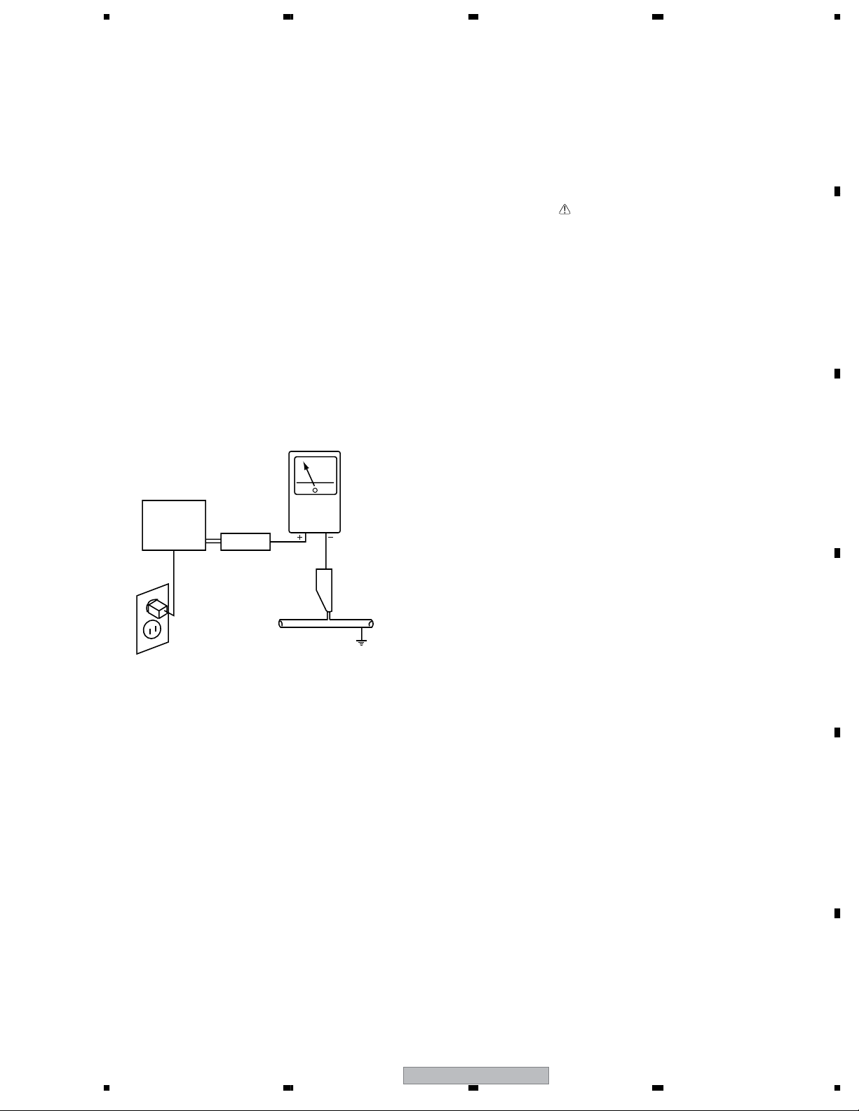
Leakage Current Cold Check
With the AC plug removed from an AC power source, place a
jumper across the two plug prongs. Turn the AC power switch on.
Using an insulation tester (DC 500V), connect one lead to the
jumpered AC plug and touch the other lead to each exposed metal
part (input/output terminals, screwheads, metal overlays, control
shafts, etc.), particularly any exposed metal part having a return
path to the chassis. Exposed metal parts having a return path to
the chassis should have a minimum resistor reading of 0.3MΩ
and a maximum resistor reading of 5MΩ. Any resistor value
below or above this range indicates an abnormality which
requires corrective action. Exposed metal parts not having a
return path to the chassis will indicate an open circuit.
Leakage Current Hot Check
Plug the AC line cord directly into an AC power source (do not
use an isolation transformer for this check).
Turn the AC power switch on.
Using a "Leakage Current Tester (Simpson Model 229
equivalent)", measure for current from all exposed metal parts of
the cabinet (input/output terminals, screwheads, metal overlays,
control shaft, etc.), particularly any exposed metal part having a
return path to the chassis, to a known earth ground (water pipe,
conduit, etc.). Any current measured must not exceed 0.5mA.
PRODUCT SAFETY NOTICE
Many electrical and mechanical parts in PIONEER set have
special safety related characteristics. These are often not evident
from visual inspection nor the protection afforded by them
necessarily can be obtained by using replacement components
rated for higher voltage, wattage, etc. Replacement parts which
have these special safety characteristics are identified in this
Service Manual.
Electrical components having such features are identified by
marking with a on the schematics and on the parts list in this
Service Manual.
The use of a substitute replacement component which dose not
have the same safety characteristics as the PIONEER
recommended replacement one, shown in the parts list in this
Service Manual, may create shock, fire or other hazards.
Product Safety is continuously under review and new instructions
are issued from time to time. For the latest information, always
consult the current PIONEER Service Manual. A subscription to,
or additional copies of, PIONEER Service Manual may be
obtained at a nominal charge from PIONEER.
A
B
C
Reading should
not be above
0.5mA
Earth
ground
Device
under
test
Also test with
plug reversed
(Using AC adapter
plug as required)
Leakage
current
tester
Test all
exposed metal
surfaces
AC Leakage Test
ANY MEASUREMENTS NOT WITHIN THE LIMITS
OUTLINED ABOVE ARE INDICATIVE OF A POTENTIAL
SHOCK HAZARD AND MUST BE CORRECTED BEFORE
RETURNING THE SET TO THE CUSTOMER.
D
E
56
PDP-505PE
F
3
7
8
1234
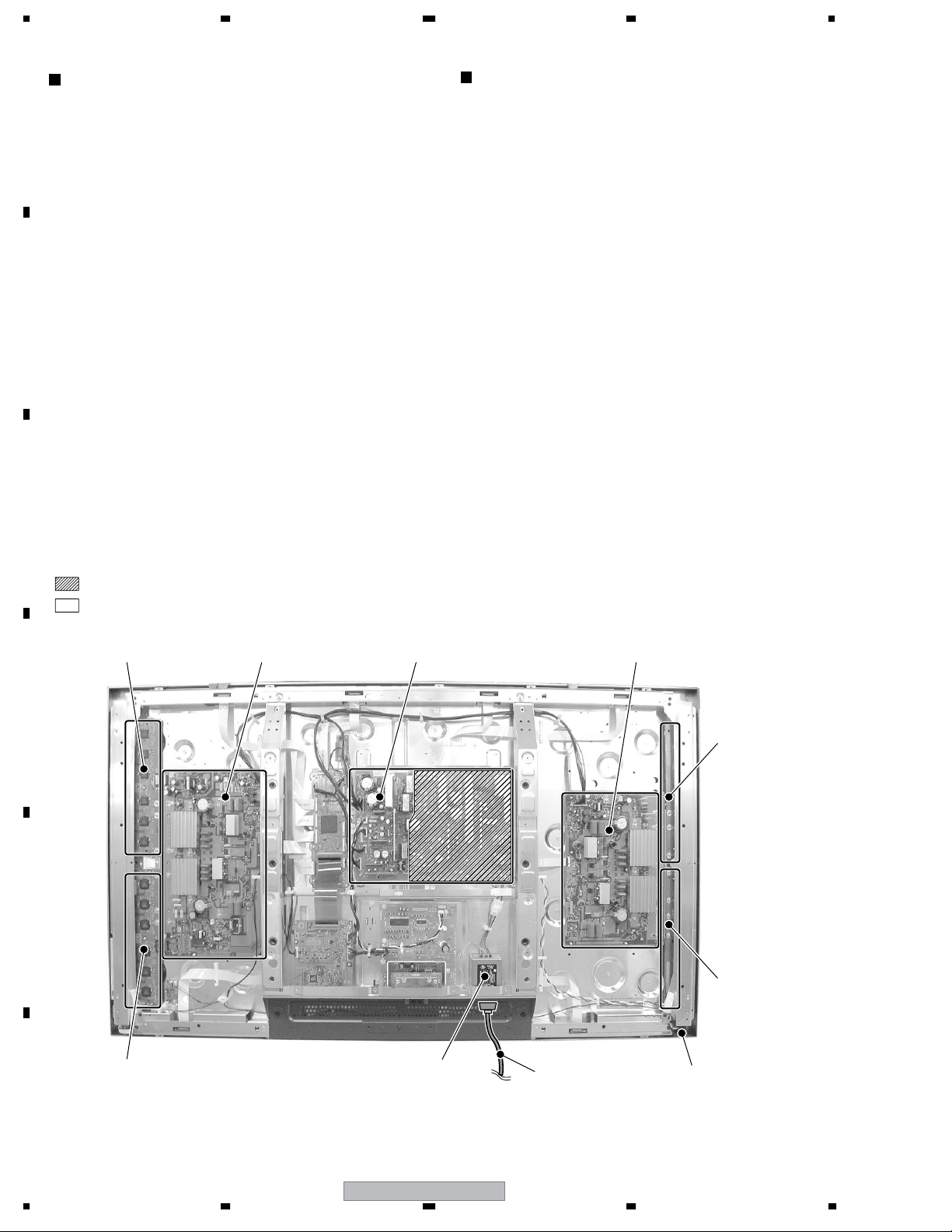
Charged Section
The places where the commercial AC power is used without
A
passing through the power supply transformer.
If the places are touched, there is a risk of electric shock. In
addition, the measuring equipment can be damaged if it is
connected to the GND of the charged section and the GND of the
non-charged section while connecting the set directly to the
commercial AC power supply. Therefore, be sure to connect the
set via an insulated transformer and supply the current.
1. AC Power Cord
2. AC Inlet with Filter
3. Power Switch (S1)
B
4. Fuse (In the POWER SUPPLY Unit)
5. STB Transformer and Converter Transformer
(In the POWER SUPPLY Unit)
6. Other primary side of the POWER SUPPLY Unit
C
: Part is Charged Section.
: Part is the High Voltage Generating Points
other than the Charged Section.
High Voltage Generating Point
The places where voltage is 100V or more except for the charged
places described above. If the places are touched, there is a risk of
electric shock.
1. POWER SUPPLY Unit................................................... (223V)
2. 50 X DRIVE Assy .......................................... (–230V to 223V)
3. 50 Y DRIVE Assy .......................................................... (353V)
4. 50 SCAN A Assy ............................................................ (353V)
5. 50 SCAN B Assy ............................................................(353V)
6. X CONNECTOR AAssy ................................ (–230V to 223V)
7. X CONNECTOR B Assy ............................... (–230V to 223V)
Discharge the VSUS voltage, as shown below:
[Method for discharging the VSUS voltage]
1. Set DRF_SW on the DIGITAL VIDEO Assy to ON (Drive
OFF status). *1, 2
2. Leave the switch at that position for about 20-30 seconds.
3. If the power is on, turn it off. Then return DRF_SW to the OFF
position. *3
Notes
*1: You can also set the unit to "Drive OFF status" by sending the
"DRF" RS232C command from the PC.
*2: DRF_SW can be switched whether the power is on or off.
*3: Power-down will occur if DRF_SW is set to OFF while the
power is on. (See "7.1.6 Power on/off function for the large-
signal system".)
POWER SUPPLY Unit50 Y DRIVE Assy50 SCAN B Assy
D
E
50 SCAN A Assy
AC Inlet with Filter
Power Cord Power Switch
50 X DRIVE Assy
X CONNECTOR
A Assy
X CONNECTOR
B Assy
(S1)
F
4
1234
Fig.1 Charged Section and High Voltage Generating Point (Rear View)
PDP-505PE
5678
[Important Check Points for Good Servicing]
In this manual, procedures that must be performed during repairs are marked with the below symbol.
Please be sure to confirm and follow these procedures.
1. Product safety
Please conform to product regulations (such as safety and radiation regulations), and maintain a safe servicing environment by
following the safety instructions described in this manual.
1 Use specified parts for repair.
Use genuine parts. Be sure to use important parts for safety.
2 Do not perform modifications without proper instructions.
Please follow the specified safety methods when modification(addition/change of parts) is required due to interferences such as
radio/TV interference and foreign noise.
3 Make sure the soldering of repaired locations is properly performed.
When you solder while repairing, please be sure that there are no cold solder and other debris.
Soldering should be finished with the proper quantity. (Refer to the example)
4 Make sure the screws are tightly fastened.
Please be sure that all screws are fastened, and that there are no loose screws.
5 Make sure each connectors are correctly inserted.
Please be sure that all connectors are inserted, and that there are no imperfect insertion.
6 Make sure the wiring cables are set to their original state.
Please replace the wiring and cables to the original state after repairs.
In addition, be sure that there are no pinched wires, etc.
7 Make sure screws and soldering scraps do not remain inside the product.
Please check that neither solder debris nor screws remain inside the product.
8 There should be no semi-broken wires, scratches, melting, etc. on the coating of the power cord.
Damaged power cords may lead to fire accidents, so please be sure that there are no damages.
If you find a damaged power cord, please exchange it with a suitable one.
9 There should be no spark traces or similar marks on the power plug.
When spark traces or similar marks are found on the power supply plug, please check the connection and advise on secure
connections and suitable usage. Please exchange the power cord if necessary.
0 Safe environment should be secured during servicing.
When you perform repairs, please pay attention to static electricity, furniture, household articles, etc. in order to prevent injuries.
Please pay attention to your surroundings and repair safely.
A
B
C
D
2. Adjustments
To keep the original performance of the products, optimum adjustments and confirmation of characteristics within specification.
Adjustments should be performed in accordance with the procedures/instructions described in this manual.
3. Lubricants, Glues, and Replacement parts
Use grease and adhesives that are equal to the specified substance.
Make sure the proper amount is applied.
4. Cleaning
For parts that require cleaning, such as optical pickups, tape deck heads, lenses and mirrors used in projection monitors, proper
cleaning should be performed to restore their performances.
5. Shipping mode and Shipping screws
To protect products from damages or failures during transit, the shipping mode should be set or the shipping screws should be
installed before shipment. Please be sure to follow this method especially if it is specified in this manual.
56
PDP-505PE
E
F
5
7
8

1234
CONTENTS
SAFETY INFORMATION..................................................................................................................................... 2
1. SPECIFICATIONS ............................................................................................................................................ 7
2. EXPLODED VIEWS AND PARTS LIST ............................................................................................................ 8
A
B
C
D
2.1 PACKING ................................................................................................................................................... 8
2.2 CHASSIS SECTION (1)........................................................................................................................... 10
2.3 CHASSIS SECTION (2)........................................................................................................................... 12
2.4 FRAME SECTION.................................................................................................................................... 14
2.5 MULTI BASE SECTION........................................................................................................................... 16
2.6 REAR SECTION ...................................................................................................................................... 18
2.7 FRONT SECTION.................................................................................................................................... 20
2.8 PANEL CHASSIS (50) Assy (AWU1092) ................................................................................................. 21
2.9 PDP SERVICE Assy 505P (AWU1097) ................................................................................................... 21
3. BLOCK DIAGRAM AND SCHEMATIC DIAGRAM (Refer to “Service Manual: ARP3215”) ............................22
3.1 BLOCK DIAGRAM ................................................................................................................................... 22
3.1.1 OVERALL BLOCK DIAGRAM ........................................................................................................... 22
3.1.2 50 Y DRIVE ASSY............................................................................................................................. 24
3.1.3 50 X DRIVE ASSY............................................................................................................................. 25
3.1.4 PANEL IF ASSY................................................................................................................................. 26
3.1.5 DIGITAL VIDEO ASSY....................................................................................................................... 31
3.1.6 HD AUDIO AMP ASSY...................................................................................................................... 33
3.2 WAVEFORMS.......................................................................................................................................... 34
4. PCB CONNECTION DIAGRAM (Refer to “Service Manual: ARP3215”)
5. PCB PARTS LIST ........................................................................................................................................... 38
6. ADJUSTMENT ............................................................................................................................................... 46
6.1 ADJUSTMENT REQUIRED WHEN THE SET IS REPAIRED OR REPLACED ....................................... 46
6.2 DRIVE ASSY ADJUSTMENT ..................................................................................................................47
6.3 COMMAND .............................................................................................................................................. 48
6.3.1 RS232C COMMAND ......................................................................................................................... 48
6.4 METHOD FOR REPLACING THE SERVICE PANEL ASSY.................................................................... 56
7. GENERAL INFORMATION............................................................................................................................. 57
7.1 DIAGNOSIS ............................................................................................................................................. 57
7.1.1 PCB LOCATION ................................................................................................................................ 57
7.1.2 DIAGNOSIS OF SHUTDOWN/POWER-DOWN INDICATED BY LEDS............................................ 58
7.1.3 DIAGNOSIS WITH THE AID OF FACTORY MODE ..........................................................................63
7.1.4 OPERATION WHEN THE MEDIA RECEIVER IS NOT CONNECTED.............................................. 65
7.1.5 TEMPERATURE-COMPENSATION FUNCTION OF THE DRIVE-SYSTEM VOLTAGE.................... 65
7.1.6 POWER ON/OFF FUNCTION FOR THE LARGE-SIGNAL SYSTEM............................................... 66
7.1.7 BACKUP WHEN THE MAIN UNIT IS ADJUSTED ............................................................................ 67
7.1.8 TROUBLESHOOTING....................................................................................................................... 70
7.1.9 DISASSEMBLY.................................................................................................................................. 71
7.2 IC INFORMATION.................................................................................................................................... 75
8. PANEL FACILITIES ...................................................................................................................................... 101
E
F
6
1234
PDP-505PE
5678
1. SPECIFICATIONS
50" Plasma Display
Item
Number of Pixels
Audio Amplifier
Surround System
Power Requirement 220-240V AC,50/60Hz,352W
Dimensions
Weight
Item
Number of Pixels
Audio Amplifier
Surround System
Power Requirement 120V AC,60Hz,363W
Dimensions
Model: PDP-505PE
1280 x 768 pixels
13 W + 13 W (1kHz, 10%, 8Ω)
SRS/FOCUS/TruBass
(0.4W Standby)
1270(W) x 737 (H) x 93 (D) mm
32.8 kg (72.3 lbs.)
Model: PRO-505PU
1280 x 768 pixels
13 W + 13 W (1kHz, 10%, 8Ω)
SRS/FOCUS/TruBass
(0.2W Standby)
1270(W) x 737 (H) x 93 (D) mm
1
/8(W)x 25 11/16(H)x 3 7/8(D)inches)
(44
A
B
C
Weight
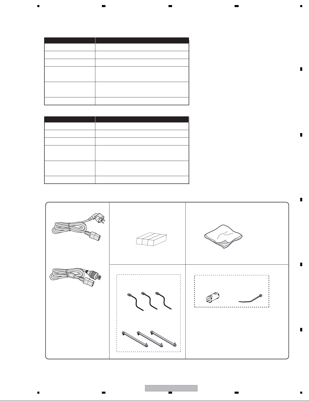
• Accessories
Power Cord
(PDP-505PE: ADG1214)
(PRO-505PU: ADG1215)
32.8 kg (72.3 lbs.)
Speaker Cushion x1
(AEB1384)
(Except PRO-505PU)
Binder Assy (AEC1908)
• Bead Bands x3
• Speed Clamp x3
Wiping Cloth x1
(AED1208)
Ferrite Core
(ATX1039)
(PDP-505PE only)
D
• Cable Tie
E
56
PDP-505PE
F
7
7
8
1234
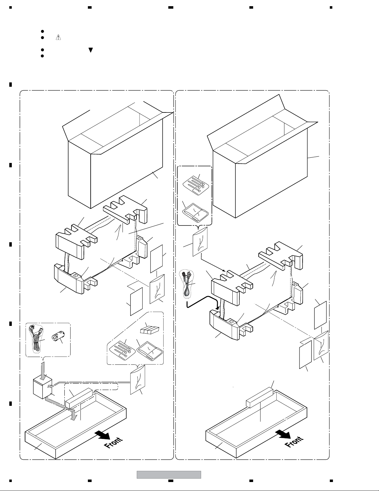
2. EXPLODED VIEWS AND PARTS LIST
NOTES:
Parts marked by "NSP" are generally unavailable because they are not in our Master Spare Parts List.
The mark found on some component parts indicates the importance of the safety factor of the part.
A
Therefore, when replacing, be sure to use parts of identical designation.
Screws adjacent to mark on product are used for disassembly.
For the applying amount of lubricants or glue, follow the instructions in this manual.
(In the case of no amount instructions, apply as you think it appropriate.)
2.1 PACKING
• PDP-505PE / WYVIXK types
B
C
• PRO-505PU / KUC type• PDP-505PE / WYVI
14
4
14
10
9
3
8
12
18
16
8
9
D
11
1
19
E
WYVIXK type only
6
5
7
17
4
3
18, 20
15
2
11
6
10
12
16
15
7
F
13
8
1234
PDP-505PE
13
>
>
>
>
5678
PACKING Parts List
No. Description Part No.
Mark
1Power Cord See Contrast table (2)
2Power Cord See Contrast table (2)
3 Wiping Cloth AED1208
4 Binder Assy AEC1908
5 Code Case See Contrast table (2)
No. Description Part No.
Mark
11 Pad See Contrast table (2)
12 Pad See Contrast table (2)
13 Carton (50) See Contrast table (2)
14 Upper Carton See Contrast table (2)
15 Vinyl Bag See Contrast table (2)
A
6 Center Pad (50) See Contrast table (2)
NSP 7 Warranty Card See Contrast table (2)
8 Mirror Mat See Contrast table (2)
9Pad See Contrast table (2)
10 Pad See Contrast table (2)
16 Caution Card ARM1232
17 Speaker Cushion See Contrast table (2)
18 Vinyl Bag S See Contrast table (2)
19 Ferrite Core See Contrast table (2)
20 Poly Bag See Contrast table (2)
(2) CONTRAST TABLE
PDP-505PE/WYVIXK, PRO-505PU/KUC and PDP-505PE/WYVI are constructed the same except for the following :
Mark No. Symbol and Description
1Power Cord ADG1214 ADG1214 Not used
2Power Cord Not used Not used ADG1215
5 Code Case AHC1041 AHC1049 Not used
6 Center Pad (50) Not used AHA2335 Not used
NSP 7 Warranty Card ARY1114 ARY1114 ARY1134
8 Mirror Mat AHG1284 AHG1327 AHG1284
9Pad (50T-L) AHA2366 Not used AHA2366
9Pad (T-L) Not used AHA2381 Not used
10 Pad (50T-R) AHA2367 Not used AHA2367
10 Pad (T-R) Not used AHA2382 Not used
PDP-505PE
WYVI
PDP-505PE
WYVIXK
PRO-505PU
KUC
B
C
11 Pad (50B-L) AHA2368 Not used AHA2368
11 Pad (B-L) Not used AHA2383 Not used
12 Pad (50B-R) AHA2369 Not used AHA2369
12 Pad (B-R) Not used AHA2384 Not used
13 Carton (50) AHD3177 AHD3191 AHD3177
14 Upper Carton (505PE) AHD3265 Not used Not used
14 Upper Carton (50) Not used AHD3271 Not used
14 Upper Carton (50EL) Not used Not used AHD3281
15 Vinyl Bag AHG1340 Not used AHG1340
17 Speaker Cushion AEB1384 AEB1384 Not used
18 Vinyl Bag S AHG1338 Not used AHG1338
19 Ferrite Core ATX1039 ATX1039 Not used
20 Poly Bag Not used AHG1326 Not used
D
E
F
56
PDP-505PE
9
7
8
1234
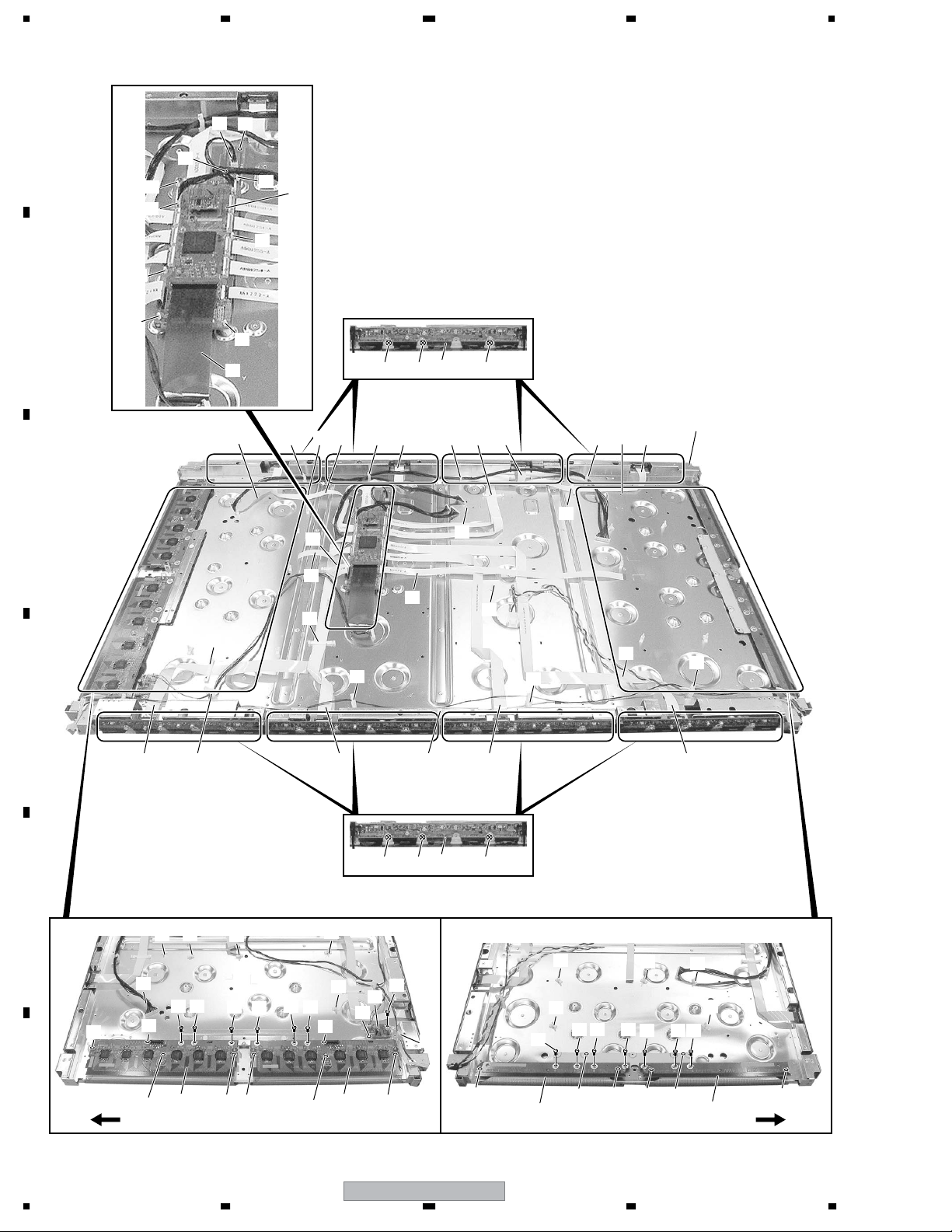
2.2 CHASSIS SECTION (1)
A
23
24
23
B
C
23
30
8
30
23
1
23
23
10
31 31 31
2734 22 11 27
22
3
2
143422 132727 12
22
28
19
20
22
22
27
D
15 16 27 17 1827
31 31 31
E
33
26
23
23
28
32
9
29
26
232324
26
23
3333 33
33
33
28
22
27
3
33
23
23
33 33 33
23
33 3333
27
23
23
2525
5
Upper
F
side
25
26 26 26
10
1234
25
4
7
PDP-505PE
25 3535 25
6
Upper
side

5678
CHASSIS SECTION (1) parts List
No. Description Part No.
Mark
1 DIGITAL VIDEO Assy AWV2074
NSP 2 P. Chassis (505) Assy AWU1092
NSP 3 50 ADDRESS Assy AWZ6870
NSP 4 50 SCAN A Assy AWZ6878
NSP 5 50 SCAN B Assy AWZ6879
NSP 6 X CONNECTOR A Assy AWZ6880
NSP 7 X CONNECTOR B Assy AWZ6881
8PANEL SENSOR Assy AWZ6872
9 KEY CONTROL Assy AWZ6844
10 FPC (114P) ADY1088
11 Flexible Cable (J201) ADD1248
12 Flexible Cable (J202) ADD1249
13 Flexible Cable (J203) ADD1250
14 Flexible Cable (J204) ADD1251
15 Flexible Cable (J205) ADD1252
16 Flexible Cable (J206) ADD1253
17 Flexible Cable (J207) ADD1254
18 Flexible Cable (J208) ADD1255
19 Flexible Cable (J209) ADD1270
20 Flexible Cable (J210) ADD1271
21 • • • • •
22 Flat Clamp AEC1879
23 PCB Spacer AEC1941
24 PCB Support AEC1938
25 PCB Spacer AEC1944
26 PCB Support AEC1958
27 Wire Saddle AEC1745
28 PCB Spacer AEC1947
29 Wire Clip AEC1948
30 Nylon Rivet AEC1671
31 Screw VBB30P080FNI
32 Screw ABZ30P060FTC
33 Screw PMB30P060FNI
34 Rear corner label AAX3081
35 Card Spacer AEC2013
A
B
C
D
56
PDP-505PE
E
F
11
7
8
1234
2.3 CHASSIS SECTION (2)
A
13
13
6
2
15
15
12
15
4
5
8
13
B
7
C
3
15
15
12
15
13
1
Upper
side
D
14
14
11
E
11
14
F
11
109
11
11
14
Upper
side
12
PDP-505PE
1234

>
5678
CHASSIS SECTION (2) parts List
No. Description Part No.
Mark
1POWER SUPPLY Unit AXY1085
2 50 X DRIVE Assy AWZ6877
3 50 Y DRIVE Assy AWV2082
4 Wire A (J101) ADX2945
5 11P Housing Wire (J102) ADX2950
6 12P Housing Wire (J103) ADX2951
7 9P Housing Wire (J106) ADX2949
8 3P Housing Wire (J109) ADX2948
9 SUB Frame L Assy (50P) ANG2638
10 SUB Frame R Assy (50P) ANG2561
11 Wire Saddle AEC1745
12 Screw PMB30P060FNI
13 Screw ABZ30P060FTC
14 Screw AMZ30P080FTC
15 Screw VBB30P080FNI
A
B
C
D
E
56
PDP-505PE
F
13
7
8
1234
2.4 FRAME SECTION
A
Upper
side
Upper
side
B
17
C
17
17
17
16
1515
17
17
17
8 9
17
16
156
17
17
17
Upper
side
17
D
10
11
1
5
14
E
17
F
17
16
15
1318
15
7
18
2
16
15
4
12
3
15
17
17
14
PDP-505PE
1234

5678
FRAME SECTION parts List
No. Description Part No.
Mark
1PANEL IR Assy AWZ6845
2PANEL LED Assy AWZ6842
3Power Switch (S1) ASG1092
4 Housing Wire (50)(J110) ADX2964
5 Flexible Cable (J211) ADD1225
6Front Chassis HU Assy (50) ANA1792
7Front Chassis HD Assy (50) ANA1793
8Front Chassis VL (50) ANA1794
9Front Chassis VR (50) ANA1795
10 Clamp AEC1884
11 Flat Clamp AEC1879
12 Switch Holder AMR3402
13 IR Holder ANG2665
14 Wire Clip AEC1948
15 Screw BPZ30P080FTB
16 Screw AMZ30P080FTC
17 Screw AMZ30P060FTB
18 Screw ABZ30P060FTC
>
A
B
C
D
E
56
PDP-505PE
F
15
7
8
1234
2.5 MULTI BASE SECTION
A
Back side
12
(Note)
12
(Note)
(Note)
12
12
12
(Note)
Note:
The No. 12 parts must be
inserted from the front
9
surface.
9
B
15
13
16
5211 14
Front side
C
D
4 615
13
13
15
17 17
7
(Note)
20
Note: When servicing, be sure to glue on the Gasket (AU)
E
17
17
17
F
16
1234
18 19
17
PDP-505PE
17
17
17
8
and make sure that they won't peel off.
(Note)
20
17
17
21
17
17
17

5678
MULTI BASE SECTION parts List
No. Description Part No.
Mark
1PANEL IF Assy AWZ6841
2 HD AUDIO AMP Assy AWZ6863
3 HD SP TERMINAL Assy AWZ6864
4AC Inlet (CN1) AKP1263
5 3P/8P Housing Wire (J104) ADX2922
6 13P Housing Wire (J105) ADX2947
7 Multi Base (P) Assy ANA1786
8 Under Cover Assy ANG2589
9 Locking Card Spacer V0 AEC2005
10 • • • • •
11 Clamp AEC1884
12 PCB Spacer AEC1941
13 HL 18 AEC1980
14 SB Spacer AEC2002
NSP 15 Wire Saddle AEC1745
16 Screw PMB30P060FNI
17 Screw AMZ30P060FTB
18 Hexagon Headed Screw BBA1051
19 Screw PMZ26P060FTB
20 Gasket (AU) ANK1745
21 Screw BPZ30P080FTB
>
A
B
C
D
E
F
56
PDP-505PE
17
7
8
1234
2.6 REAR SECTION
A
7
8
6
8
6
2 2
1
6
8
8
6
8
6
8
6
8
8
B
8
6
8
C
6
6
8
8
8
8 6
3
8 8
6 6
5
8
4
8
8
8
8
8
6
6
8
6
6
6
8
6
8
D
E
F
18
PDP-505PE
1234
5678
REAR SECTION parts List
No. Description Part No.
No. Description Part No.
Mark
1 Rear Case (50P) ANE1626
2 Inner Grip Assy AMR3434
NSP 3 Name Label See Contrast table (2)
4Volt caution Label See Contrast table (2)
5Terminal Label See Contrast table (2)
Mark
6 Screw ABZ30P100FTB
7 Serial Sheet AAX3143
8 Screw AMZ30P060FTB
(2) CONTRAST TABLE
PDP-505PE/WYVIXK, PRO-505PU/KUC and PDP-505PE/WYVI are constructed the same except for the following :
Mark No. Symbol and Description
NSP 3 Name Label AAL2568 AAL2580 AAL2570
4Volt Caution Label AAX3117 AAX3005 AAX3117
5Terminal Label AAX2998 AAX3006 AAX2997
PDP-505PE
WYVI
PDP-505PE
WYVIXK
PRO-505PU
KUC
A
B
C
D
E
56
PDP-505PE
F
19
7
8
1234
2.7 FRONT SECTION
A
8
2
4
B
6
3
• Rear view
C
7
8
5
8
5
8
5
8
8
1
5
4
D
FRONT SECTION parts List
No. Description Part No.
No. Description Part No.
Mark
1PANEL KEY Assy AWZ6843
2Front Case Assy See Contrast table (2)
3Power Button AAD4127
E
NSP 4 Panel Holder V (50) ANG2663
5Panel Holder H Assy 50 See Contrast table (2)
Mark
6 Coil Spring ABH1114
7 Blind Cushion AEB1383
8 Screw ABZ30P060FTC
(2) CONTRAST TABLE
PDP-505PE/WYVIXK, PRO-505PU/KUC and PDP-505PE/WYVI are constructed the same except for the following :
Mark No. Symbol and Description
2Front Case Assy (50PE) AMB2834 AMB2834 Not used
2Front Case Assy (50EL) Not used Not used AMB2836
F
5Panel Holder H Assy 50 ANG2678 Not used ANG2678
5Panel Holder H Not used ANG2662 Not used
5 Gasket Not used ANK1740 Not used
PDP-505PE
WYVI
PDP-505PE
WYVIXK
PRO-505PU
KUC
20
PDP-505PE
1234
5678
2.8 PANEL CHASSIS (50) Assy (AWU1092)
PANEL CHASSIS (50) Assy (AWU1092) parts List
No. Description Part No.
Mark
NSP 1..50 ADDRESS Assy AWV2080
NSP 2..50 ADDRESS Assy AWZ6870
NSP 1..50 SCAN Assy AWV2083
NSP 2..50 SCAN A Assy AWZ6878
NSP 2..50 SCAN B Assy AWZ6879
NSP 2..X CONNECTOR A Assy AWZ6880
NSP 2..X CONNECTOR B Assy AWZ6881
NSP P. Panel (50LC) Assy AWU1103
NSP Adress Module (IC1-IC40) AXF1129
NSP FPC (50XGA-X) ADY1084
NSP FPC (50XGA-Y) ADY1085
NSP Chassis Assy (505) ANA1803
PCB Spacer AEC1944
PCB Support AEC1958
Edge Card Spacer AEC1998
Mark
Rivet (Plastic) AMR1066
FC Spacer AMR3370
NSP Adhesive ZBA-KE3424S
NSP Lotion ZLX-AP7
NSP Tape ZTA-8101-12
NSP Double Faced Tape ZTB-5015-18
NSP Tape ZTC-POLYCA-20
NSP Tape ZTC-900UL-15
NSP Silicone Rubber ZTX-HC20-15
NSP Silicone Rubber ZTX-HC50-15
NSP Wiping Cloth ZTX-MX100-13
NSP Film
NSP Film ZTX-2102Y45-5
No. Description Part No.
NSP Silicone Rubber
A
ZTC-EM7KB0R85T-15W
B
ZTX-2102Y35-2R5
2.9 PDP SERVICE Assy 505P (AWU1097)
PDP SERVICE Assy 505P (AWU1097) parts List
NSP 1..P.Chassis (505) Assy AWU1092
1..Front Chassis HU Assy (50) ANA1792
1..Front Chassis HD Assy (50) ANA1793
1..Front Chassis VL (50) ANA1794
1..Front Chassis VR (50) ANA1795
1..Sub Frame L Assy (50P) ANG2638
1..Sub Frame R Assy (50P) ANG2561
1..Wire Saddle AEC1745
1..PCB Support AEC1938
1..PCB Spacer AEC1941
1..PCB Spacer AEC1947
1..Wire Clip AEC1948
1..Card Spacer AEC2013
1..Caution Label AAX3031
1..Drive Voltage Label ARW1097
1..Screw ABZ30P100FTB
1..Screw AMZ30P060FTB
1..Screw AMZ30P080FTC
1..Screw VBB30P080FNI
1..Screw BPZ30P080FTB
NSP 1..Front Case Assy (50SVC) AMB2849
2..Panel Cushion H (50) AED1257
2..Panel Cushion V (50) AED1258
NSP 2..Front Case (50P) AMB2823
1..Rear Case (50P) ANE1614
NSP 1..Vinyl Pouch AHG-195
1..Pad (50T-L) AHA2366
1..Pad (50T-R) AHA2367
1..Pad (50B-L) AHA2368
1..Pad (50B-R) AHA2369
1..Carton(50) AHD3177
1..Upper Carton (505SVC) AHD3290
1..Protect Sheet AHG1331
1..Rear corner label(15) AAX3081
C
D
E
F
56
PDP-505PE
21
7
8
1234
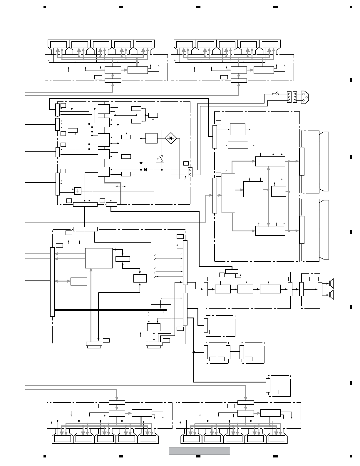
3. BLOCK DIAGRAM AND SCHEMATIC DIAGRAM
3.1 BLOCK DIAGRAM
3.1.1 OVERALL BLOCK DIAGRAM
A
DRIVER IC
IC1551
DRIVER IC
IC1552
DRIVER IC
IC1553
DRIVER IC
IC1554
DRIVER IC
IC1555
DRIVER IC
IC1551
DRIVER IC
IC1552
DRIVER IC
IC1553
DRIVER IC
IC1554
DRIVER IC
IC1555
V+5V
V+3V_IC5
V+3V_PLLV+3V_LVDS
AD1
IC1501
CN1501
V+ADR
RESONANCE
50 ADDRESS ASSY
V+9V
BLOCK
V+60V
V+5V
V+9V
V+3V_IC5
V+3V_PLLV+3V_LVDS
AD1
IC1501
CN1501
V+ADR
RESONANCE
BLOCK
50 ADDRESS ASSY
V+60V
PANEL SENSOR ASSY
SENSOR
IC1072
B
50 SCAN B ASSY
VCC
_VH
VCC
_VH
VCC
_VH
VCC
_VH
VCC
_VH
VCC
_VH
VCC
_VH
VCC
_VH
VCC
_VH
VCC
_VH
VCC
_VH
VCC
_VH
PSUS
PSUS
SB1 Y2
SCAN
CN3201
SCAN
CN3001
SA1 Y3
CN2101
CN2102
IC5V
ADD
SEL_PULSE
IC3201
IC5V
ADD
SEL_PULSE
IC3202
IC5V
ADD
SEL_PULSE
IC3203
C
D
E
IC5V
ADD
SEL_PULSE
IC3204
IC5V
ADD
SEL_PULSE
IC3205
IC5V
ADD
SEL_PULSE
IC3206
IC5V
ADD
SEL_PULSE
IC3001
IC5V
ADD
SEL_PULSE
IC3002
IC5V
ADD
SEL_PULSE
IC3003
IC5V
ADD
SEL_PULSE
IC3004
IC5V
ADD
SEL_PULSE
IC3005
IC5V
ADD
SEL_PULSE
IC3006
50 SCAN A ASSY
CN1071
TE1
V_IC5V
VCC_VH
+16.5V
+5V
PSUSPSUS
MASK MOD
IC2307
+16.5V
SOFT-D
BLOCK
+16.5V
VSUS
+RESET
BLOCK
+5V +15V VSUS
MASK MOD
+5V +16.5V V_OFS
VCC_VH
V_IC5V
Scan Signal
50 Y DRIVE ASSY
V_OFS
VC_VF-
VC_VF+
+5V
VSUS
Drive
Signal
+5V
+16.5V
RESONANCE
BLOCK
IC2303
OFFSET
BLOCK
V_IC5V
Photo Coupler
BLOCK
DC_DC
CONV
BLOCK
REGULATOR
Drive
Signal
Drive
Signal
V_IC5VVCC_VH
LOGIC
BLOCK
VSUS
+5V
Y4
CN2301
+6.5V
Y1 D13
SCAN
YSUS
CN2001
VH_UV_PD
YDRIVE_PD
YRESNC_PD
YDD_CHV_PD
IC5V_UV_PD
CN5501
ADR_
PD0
OR
CN5202
D4
CN5521
OR
ADR_
PD4
CN5505
D5
ADR_PD1
LVDS
V+3V_D
V+1V_D
DCC_PD
FLASH MEMORY
SUB-FILD CONV.
XY DRV SEQUENCE
PATTERN GEN.
OR
Vofs
MODULE UCOM
LVDS
ADR_PD5
D9
CN5502
D6
ADR_PD2
CN5503
DIGITAL VIDEO ASSY
V+12V
DC-DC
CONVERTER
MODULE
AXY1086
IC5305
IC5401
PEG054A
IC5201
CN5506
&
PSIZU
ADR_PD6
D10
OR
OR
PD_MUTE
RELAY, PD_TRIGGER
CN5507
D7
ADR_PD3
PD
ADR_PD7
D11
CN5504
V+60V
V+6.5V
V+12V
Vsus_ADJ.
PD_PWDN
XSUS
XSUSTN_PD
XDD_CNV_PD
XDRIVE_PD
DCLK, DE
HD, VD
RA IN, GA IN, BA IN
RB IN, GB IN, BB IN
CN5508
D8
D15
D12
D2
CN5601 CN5602
D1
D14
CN5511
CN5001
CN1501
AD1
V+3V_PLLV+3V_LVDS
F
V+5V
DRIVER IC
IC1551
DRIVER IC
IC1552
V+3V_IC5
DRIVER IC
IC1553
22
50 ADDRESS ASSY
DRIVER IC
IC1554
RESONANCE
BLOCK
V+ADR
IC1501
PDP-505PE
V+9V
DRIVER IC
IC1555
V+60V
V+5V
DRIVER IC
IC1551
V+3V_PLLV+3V_LVDS
DRIVER IC
IC1552
AD1
V+3V_IC5
DRIVER IC
IC1553
CN1501
50 ADDRESS ASSY
DRIVER IC
IC1554
RESONANCE
V+ADR
IC1501
BLOCK
DRIVER IC
IC1555
V+9V
V+60V
1234
5678
DRIVER IC
IC1551
V+5V
RA IN, GA IN, BA IN
RB IN, GB IN, BB IN
CN4004
DRIVER IC
IC1552
V+3V_PLLV+3V_LVDS
P4
VSUS
+6.5V
+16.5V
M601
VSUS_
P3
CONT
P5
+6.5V
VADR
P2
Vsus_ADJ.
+12V
PS.PD
EXT.PD
RELAY
STB
3.3V
P1 P6
CN4001
R1
V+3V
V+6.5V
ACTV
R4
DCLK, DE
HD, VD
EEPROM
for Backup
B_SDA
B_SCL
DRIVER IC
V+3V_IC5
AD1
SECONDARY
+6.5V
TMDS RECEIVER
IC4202
TMDS
CN4003
IC1553
STB3.3
MUTE
DDC
DRIVER IC
IC1501
CN1501
T5
T4
T2
T3
T1
PANEL IF ASSY
FET SW
R3
IC1554
DRIVER IC
V+ADR
RESONANCE
BLOCK
IC1555
V+9V
V+60V
50 ADDRESS ASSY
Switching
Q14
Q13
+390V
D133
D31,D32
M341
PFC
Q1,Q2
RL1
RELAY
& PD
Switching
Q11
Switching
Q12
Switching
M1
Switching
PRIMARY
POWER SUPPLY UNIT
A_SCL,A_SDA,SRS
Bus
Buffer
Bus
V+3V_STB
Buffer
CN4002
MDR CONNECTORDVI CONNECTOR
V+5V
RC1
NEUTRAL
V+6.5V
FOCUS,TRUBASS
A_MUTE
ST_BY
A_NG
AUDIO L
AUDIO R
LED_R,G
KEY
REM
STB
_MT
R2
DRIVER IC
IC1551
P7
LIVE
R7
CN4009
CN4010
R8
DRIVER IC
IC1552
DRIVER IC
IC1553
V+3V_IC5
V+3V_PLLV+3V_LVDS
AD1
DRIVER IC
IC1554
V+ADR
IC1501
CN1501
RESONANCE
50 ADDRESS ASSY
LIVE
NEUTRAL
DRIVER IC
IC1555
BLOCK
MAIN POWER
V+9V
S1
V+60V
50 X DRIVE ASSY
X2
DC_DC
VSUS
CONV
BLOCK
+6.5V
REGULATOR
Drive
+5V
Signal
X1
LOGIC
BLOCK
CN1001 CN1201
CN3504
A4
+9V
A1 A3 SP2 SP1
L,R
WOW IC
IC3501
L,R
Drive
Signal
+16.5V
RESONANCE
BLOCK
+16.5V
+9V
VOL IC
IC3502
V_RN
+5V
+16.5V
MASK MOD
IC1203
V_RN
-RESET
+16.5VVSUS
IC1207
+16.5V
IC3504
+16.5V
PULSE
BLOCK
+5V
+5V
VSUS
SUS
OUT
+5V
SUS
OUT
MASK MOD
L,R L,R
POWER AMP
PSUS
PSUS
L,R L,R
CN3503
HD AUDIO AMP ASSY
PANEL
LED
CN4751 CN3501
ASSY
L1
CN4852
KL2 KL1 SW1
KEY CONTROL
ASSY
CN4851
CN4801
PANEL KEY
ASSY
PANEL IR
CN4901
RE1
ASSY
AC INLET
X CONNECTOR
A ASSY
X CONNECTOR
B ASSY
J3701
CN3701
HD SP TERMINAL
ASSY
A
B
C
D
SPEAKER
E
V+5V
DRIVER IC
IC1551
CN1501
V+3V_PLLV+3V_LVDS
DRIVER IC
IC1552
AD1
V+3V_IC5
DRIVER IC
IC1553
50 ADDRESS ASSY
DRIVER IC
IC1554
RESONANCE
BLOCK
V+ADR
IC1501
DRIVER IC
IC1555
V+9V
V+60V
V+5V
DRIVER IC
IC1551
V+3V_PLLV+3V_LVDS
DRIVER IC
IC1552
PDP-505PE
56
AD1
V+3V_IC5
DRIVER IC
IC1553
7
CN1501
50 ADDRESS ASSY
DRIVER IC
IC1554
RESONANCE
V+ADR
IC1501
BLOCK
DRIVER IC
IC1555
V+9V
V+60V
F
23
8
1234
3.1.2 50 Y DRIVE ASSY
• Block Diagram
A
50 Y DRIVE ASSY
Y1
IC5V
VH
Y2
To
50 SCAN B ASSY
CN2101CN2102
CE
B
C
D
CLK2
CLR
OC2
OC1
YPR-U
YSOFT-D
YSUS-G
YSUS-B
YSUS-U2
From DIGITAL VIDEO ASSY
YSUS-D2
YSUS-U1
YSUS-D1
YSUS-MSK
YOFS
YSUS-PD
SCN_5V_PD
Y_DD_PD
SCAN_PD
YDRIVE_PD
Photo CouplerCLK1
Photo Coupler
Photo Coupler
Photo Coupler
Photo Coupler
Photo Coupler
SI
Photo Coupler
CN2001
VH
Y3
YSUS
-U2
5V
YSUS-D2
YSUS-U1
5V
YSUS-D1
To
50 SCAN A ASSY
YPR-U
YSOFT-D
IC2202
HB
DRIVER
SUS
HB
XSUS
P.D.
Circuit
GND
SUS
GND
IC2201
DRIVER
IC2203
YSUS-G
YSUS-B
L2204
L2202
VSUS
L2205
L2203
VSUS
16.5V
VSUS
16.5V
5V
5V
Mask Module
IC2303
STK795-513A
Mask Module
IC2307
STK795-513A
To
SCAN ASSY
YSUS-MSK
YOFS
IC2302
Photo
Coupler
IC2304
IC2311
E
Y4
CN2301
1
16.5V
2
DGND
3
6.5V
DGND
4
N.C.
5
6
N.C.
7
VSUS VSUS
VSUS
8
N.C.
9
F
SUSGND
SUSGND
From POWER SUPPLY UNIT
10
11
P.D.
DET.
IC2305
REGULATOR
IC5V UVP
5V
VOFS OVP
VOFS UVP
VH OVP
VH UVP
VSUS
IC5V, VF
D-D CONV.
D-D CONV.
VH D-D
CONV.
24
VOFS
VF+
VF-
IC5V
VOFS
VH
PDP-505PE
1234
5678
3.1.3 50 X DRIVE ASSY
• Block Diagram
A
X1
XSUS-G
XSUS-B
XSUS-U2
XSUS-D2
XSUS-U1
XSUS-D1
XSUS-MSK
XCP-MSK
XSUS_PD
XDD_PD
XDRV_PD
From DIGITAL VIDEO ASSY
SUSGND
SUSGND
From POWER SUPPLY UNIT
CN1001
XNR-D
X2
CN1201
1
16.5V
2
DGND
3
6.5V
DGND
4
N.C.
5
6
N.C.
7
VSUS VSUS
VSUS
8
N.C.
9
10
11
12
N.C.
50 X DRIVE ASSY
P.D.
DET.
IC1205
REGULATOR
5V
VRN UVP P.D.
XNR-D
VRN OVP
P.D.
XSUS
-U2
5V
XSUS-D2
XSUS-U1
5V
XSUS-D1
XCP-MSK
XSUS-MSK
VSUS
D-D CONV.
T1401
IC1101
HB
DRIVER
IC1102
HB
DRIVER
XSUS
P.D.
Circuit
Charge Pump
Circuit
IC1202
Photo
Coupler
IC1204
VRN-235V
SUS
GND
SUS
GND
VCP
XSUS-G
XSUS-B
L1102
L1104
L1103
L1105
VSUS
16.5V
VSUS
16.5V
5V
5V
Mask Module
IC1203
STK795-512A
Mask Module
IC1207
STK795-512A
PSUS
To
X CONNECTOR ASSY
B
C
D
56
PDP-505PE
E
F
25
7
8
1234
3.1.4 PANEL IF ASSY
• Block Diagram
A
PANEL IF ASSY
R3
TMDS
CN4003CN4002
6: DDC_SCL
7: DDC_SDA
B
C
DVI CONNECTOR
14: DDC_+5V
11: MTXD
2: MRXD
3: P_ST_B
10: MR_ST_B
7: REQ
8: STB3V
9: KEY_B
14: REM_B
MDR CONNECTOR
15: STB_MT
I2C BUFFER
R2
IC4006 BUF
IC4006 BUF
IC4006 BUF
IC4006 BUF
Q4004 INV
Q4006 INV
Q4006 INV
Q4009 INV
D
IC4202
TMDS RECEIVER
IC4206
Q4004
INV
Q4215
5V ↔ 3.3V
I2C LEVEL SHIFT
Q4007,
Q4011
NOR
Q4017
INV
IC4205
RESET IC
Q4006 INV
Q4006 INV
IC4002
BACKUP ROM
IC4006 BUF
IC4006 BUF
Q4011 INV
Q4001
5V ↔ 3.3V
I2C LEVEL SHIFT
R4
RSTBTMD
DVI_MUTE
DVI_OFF
RXD0
TXD0
B_SCL, B_SDA
CN4004CN4009
MR_ST_B
REQ_MD
MR_AC_OFF
KEY_B
REM_B
LED_R_B
LED_G_B
A_NG,A_MUTE,STB_SW,
FOCUS,TRUBASS,SRS
A_SCL, A_SDA
R7
13: AUDIO_R
20: AUDIO_L
R8
REM
CN4010
KEY
LED R
LED G
R_IN
L_IN
E
F
26
PDP-505PE
1234
5678
• Voltages
CN4001 (R1) < ⇔ POWER SUPPLY UNIT >
No. Signal Name I/O Signal Description Voltages at NTSC Signal Input
1 6.5V I +6.5V power supply +6.8VDC
2 6.5V I +6.5V power supply +6.8VDC
3 Vcc_GND − GND
4 Vcc_GND − GND
5 STB3.3V I Power supply +3.3V input of module UCOM at panel side +3.3VDC
6 STB_GND − GND
7 STB3.3MUTE O Standby control (+3.3V mute) +3.3 VDC
8 AC_DET I Primary power supply (AC) state input at panel side +3.0VDC
CN4002 (R2) < ⇔ MEDIA RECEIVER >
No. Signal Name I/O Signal Description Voltages at NTSC Signal Input
1 MR_ST_B I
2 MRXD O
3 P_ST_B O
4 ACT3V O
5 AC_OFF O
6 GND
7 REQ O
8 STB3V I
9 KEY_B O
10 MR_ST_B' I
11 MTXD I
12 GND
13 AUDIO_R I
14 REM_B O
15 STB_MT I
16 GND
17 NC
18 FIELD I
19 GND
20 AUDIO_L I
Connection state detecting signal with MR
UART communication transmission data with the main UCOM (external PC)
at MR side
Connection state output for the MR
Power supply +3.3V output of module UCOM at panel side
Primary power supply (AC) state output at panel side
−
GND
Communication request to the main UCOM (external PC) at the MR
Standby power supply (+3.3V) input from the MR
Function key code signal output at panel side
Connection state detecting signal with the MR
UART communication receive data with the main UCOM (external PC) at
the MR side
−
GND
R ch audio signal input Audio R signal
Remote control code signal output
Standby control input
−
GND
−
Not connected
FIELD control signal
−
GND
L ch audio signal input Audio L signal
0VDC
0-3.3V amplitude square wave
0VDC
+3.3VDC
0VDC
0-3.3V amplitude square wave
+3.3VDC
0-3.3V amplitude square wave (at key
operation)
0VDC
0-3.3V amplitude square wave
0-3.3V amplitude square wave (at remocon
code transmission)
0VDC
−
0VDC
A
B
C
D
CN4003 (R3) < ⇔ MEDIA RECEIVER >
No. Signal Name I/O Signal Description Voltages at NTSC Signal Input
1 RX2- I
2 RX2+ I
3 GND
4 N.C
5 N.C
6 DDC_SCL I
7 DDC_SDA I
8 N.C
9 RX1- I
10 RX1+ I
11 GND
12 N.C
13 N.C
14 DDC_+5V I
15 GND
16 HPD O
17 RX0- I
18 RX0+ I
19 GND
20 N.C
21 N.C
56
DVI signal DVI differential signal (-)
DVI signal DVI differential signal (+)
−
GND
−
Not connected
−
Not connected
I2C signal for DDC
I2C signal for DDC 0-5V amplitude square wave
−
Not connected
DVI signal DVI differential signal (-)
DVI signal DVI differential signal (+)
−
GND
−
Not connected
−
Not connected
I2C power supply for DDC
−
GND
Hot plug detection
DVI signal DVI differential signal (-)
DVI signal DVI differential signal (+)
−
GND
−
Not connected
−
Not connected
−
−
0-5V amplitude square wave
−
−
−
+5VDC
+5VDC
−
−
PDP-505PE
7
8
E
F
27
1234
• Voltages
CN4003 (R3) < ⇔ MEDIA RECEIVER >
A
No. Signal Name I/O Signal Description Voltages at NTSC Signal Input
22 GND
23 RXC+ I
24 RXC- I
CN4009 (R7) < ⇔ HD AUDIO AMP ASSY >
No. Signal Name I/O Signal Description Voltages at NTSC Signal Input
1 A_NG I
2 V+6.5 O
3 GNDA
4 L_IN O
B
5 GNDA
6 R_IN O
7 ST_BY O
8 A_MUTE O
9 SCL O
10 SDA O
11 FOCUS O
12 SRS O
13 TRUBASS O
−
GND
DVI signal DVI differential signal (-)
DVI signal DVI differential signal (+)
Abnormal detecting signal of the audio block
+6.5V power supply
−
GND
L ch audio signal Audio L signal
−
GND
R ch audio signal Audio R signal
Standby signal of the audio block +3.3V DC
Audio mute signal input 0V DC
I2C control signal for audio 0-3.3V amplitude square wave
I2C control signal for audio 0-3.3V amplitude square wave
Focus function control signal +3.3V DC
SRS function control signal +3.3V DC
TRUBASS function control signal +3.3V DC
+3.3V DC
+6.8V DC
CN4010 (R8) < ⇔ PANEL LED ASSY, PANEL IR ASSY, KEY CONTROL ASSY >
C
No. Signal Name I/O Signal Description Voltages at NTSC Signal Input
1 LED_G O
2 LED_R O
3 AC_OFF O
4 STB3V O
5 STBGND
6 REM I
7 STB+3V O
8 KEY I
9 STBGND
D
LED control (green)
LED control (red)
Primary power supply (AC) state output at the panel side
+3.3V power supply +3.3V DC
− GND
Remote control code signal input
+3.3V power supply +3.3V DC
Function key code signal input at the panel side
− GND
+2.1VDC
0VDC
0VDC
0-3.3V amplitude square wave (at remocon
code transmission)
0-3.3V amplitude square wave (at key operation)
CN4801 (SW1) < ⇔ KEY CONTROL ASSY >
No. Signal Name I/O Signal Description Voltages at NTSC Signal Input
1 STBGND
2G1 O
3G0 O
4D5 I
5D6 I
6D7 I
E
−
GND 0V DC
Key scan signal 0V DC
Key scan signal 0V DC
Key scan signal +3.3V DC
Key scan signal +3.3V DC
Key scan signal +3.3V DC
F
28
1234
PDP-505PE

5678
• Voltages
CN4004 (R4) < ⇔ DIGITAL VIDEO ASSY > (1/2)
No. Signal Name I/O Signal Description Voltages at NTSC Signal Input
1 GND
2 GND
3
GND
GND
4
5 BA0 O
6 BA1 O
7 BA2 O
8 BA3 O
9 BA4 O
10 BA5 O
11 BA6 O
12 BA7 O
13 GND
14 GND
GND
15
GND
16
17 GA0 O
18 GA1 O
19 GA2 O
20 GA3 O
21 GA4 O
22 GA5 O
23 GA6 O
24 GA7 O
25 GND
26 GND
GND
27
GND
28
29 RA0 O
30 RA1 O
31 RA2 O
32 RA3 O
33 RA4 O
34 RA5 O
35 RA6 O
36 RA7 O
37
GND\
38 DCLK O
39 GND
40 DEI O
41 HDI O
42 VDI O
43 FIELD O
44 APL_DT
45
GND
GND
46
47 BB0 O
48 BB1 O
49 BB2 O
50 BB3 O
51 BB4 O
52 BB5 O
53 BB6 O
54 BB7 O
55 GND
56 GND
57
GND
GND
58
−
GND
−
GND
−
GND
−
GND
8bit video signal output (BLUE even number) 0-3.3V amplitude square wave
8bit video signal output (BLUE even number) 0-3.3V amplitude square wave
8bit video signal output (BLUE even number) 0-3.3V amplitude square wave
8bit video signal output (BLUE even number) 0-3.3V amplitude square wave
8bit video signal output (BLUE even number) 0-3.3V amplitude square wave
8bit video signal output (BLUE even number) 0-3.3V amplitude square wave
8bit video signal output (BLUE even number) 0-3.3V amplitude square wave
8bit video signal output (BLUE even number) 0-3.3V amplitude square wave
−
GND
−
GND
−
GND
−
GND
8bit video signal output (GREEN even number) 0-3.3V amplitude square wave
8bit video signal output (GREEN even number) 0-3.3V amplitude square wave
8bit video signal output (GREEN even number) 0-3.3V amplitude square wave
8bit video signal output (GREEN even number) 0-3.3V amplitude square wave
8bit video signal output (GREEN even number) 0-3.3V amplitude square wave
8bit video signal output (GREEN even number) 0-3.3V amplitude square wave
8bit video signal output (GREEN even number) 0-3.3V amplitude square wave
8bit video signal output (GREEN even number) 0-3.3V amplitude square wave
−
GND
−
GND
−
GND
−
GND
8bit video signal output (RED even number) 0-3.3V amplitude square wave
8bit video signal output (RED even number) 0-3.3V amplitude square wave
8bit video signal output (RED even number) 0-3.3V amplitude square wave
8bit video signal output (RED even number) 0-3.3V amplitude square wave
8bit video signal output (RED even number) 0-3.3V amplitude square wave
8bit video signal output (RED even number) 0-3.3V amplitude square wave
8bit video signal output (RED even number) 0-3.3V amplitude square wave
8bit video signal output (RED even number) 0-3.3V amplitude square wave
−
GND
Synchronous signal output (clock) 0-3.3V amplitude square wave (42.5MHz)
−
GND
Synchronous signal output (data enable)
Synchronous signal output (Horizontal sync.)
Synchronous signal output (Vertical sync.)
FIELD control signal 0V DC
Not connected
−
GND
−
GND
8bit video signal output (BLUE odd number) 0-3.3V amplitude square wave
8bit video signal output (BLUE odd number) 0-3.3V amplitude square wave
8bit video signal output (BLUE odd number) 0-3.3V amplitude square wave
8bit video signal output (BLUE odd number) 0-3.3V amplitude square wave
8bit video signal output (BLUE odd number) 0-3.3V amplitude square wave
8bit video signal output (BLUE odd number) 0-3.3V amplitude square wave
8bit video signal output (BLUE odd number) 0-3.3V amplitude square wave
8bit video signal output (BLUE odd number) 0-3.3V amplitude square wave
−
GND
−
GND
−
GND
−
GND
−
−
−
−
−
−
−
−
−
−
−
−
−
−
0-3.3V amplitude square wave (positive polarity)
0-3.3V amplitude square wave (negative polarity)
0-3.3V amplitude square wave (negative polarity)
−
−
−
−
−
−
−
A
B
C
D
E
F
56
PDP-505PE
29
7
8

1234
• Voltages
CN4004 (R4) < ⇔ DIGITAL VIDEO ASSY > (2/2)
A
No. Signal Name I/O Signal Description Voltages at NTSC Signal Input
59 GB0 O
60 GB1 O
61 GB2 O
62 GB3 O
63 GB4 O
64 GB5 O
65 GB6 O
66 GB7 O
67 GND
68 GND
B
C
D
E
F
GND
69
70
GND
71 RB0 O
72 RB1 O
73 RB2 O
74 RB3 O
75 RB4 O
76 RB5 O
77 RB6 O
78 RB7 O
79 GND
80 MASK
81 MODE
82 MODEL
83 DITHER
84 V+3VACTV O Power supply +3.3V output of module UCOM at panel side +3.3VDC
85 B_SDA I E2PROM control signal for backup
86 RXD0 O
87 REM_B O Remote control code signal output
88 TXD0 I
89 KEY_B O Function key code signal output at panel side
90 REQ_MD I
91 LED_R_B I LED control (red) +3.3VDC
92 MR_AC_OFF O AC state output at MR side 0VDC
93 LED_G_B I LED control (green) 0VDC
94 POWER Not connected −
95 DVI_MUTE I DVI mute signal input 0VDC
96 MR_ST_B O Connection state detecting signal with MR 0VDC
97 A_MUTE I Audio mute signal input 0VDC
98 OP_DET
99 A_NG O Abnormal detecting signal of audio block +3.3VDC
100 PNL_MUTE Not connected −
101 A_SCL I I2C control signal for audio
102 STB_SW I Standby signal of audio block +3.3VDC
103 A_SDA I I2C control signal for audio
104 DDC_WP I
105 TRUBASS I TRUBASS function control signal +3.3VDC
106 B_SCL I E2PROM control signal for backup
107 FOCUS I FOCUS function control signal +3.3VDC
108 DVI_OFF O Connection detecting signal of DVI connector 0VDC
109 SRS I SRS function control signal +3.3VDC
110 RSTBTMD O TMDS IC reset signal +3.3VDC
111 MAX_PLS1 Not connected −
112 L_SYNC O TMDS IC synchronous detecting signal +3.3VDC
113 MAX_PLS2 Not connected −
114 GND
8bit video signal output (GREEN odd number) 0-3.3V amplitude square wave
8bit video signal output (GREEN odd number) 0-3.3V amplitude square wave
8bit video signal output (GREEN odd number) 0-3.3V amplitude square wave
8bit video signal output (GREEN odd number) 0-3.3V amplitude square wave
8bit video signal output (GREEN odd number) 0-3.3V amplitude square wave
8bit video signal output (GREEN odd number) 0-3.3V amplitude square wave
8bit video signal output (GREEN odd number) 0-3.3V amplitude square wave
8bit video signal output (GREEN odd number) 0-3.3V amplitude square wave
−
GND
−
GND
−
GND
−
GND
8bit video signal output (RED odd number) 0-3.3V amplitude square wave
8bit video signal output (RED odd number) 0-3.3V amplitude square wave
8bit video signal output (RED odd number) 0-3.3V amplitude square wave
8bit video signal output (RED odd number) 0-3.3V amplitude square wave
8bit video signal output (RED odd number) 0-3.3V amplitude square wave
8bit video signal output (RED odd number) 0-3.3V amplitude square wave
8bit video signal output (RED odd number) 0-3.3V amplitude square wave
8bit video signal output (RED odd number) 0-3.3V amplitude square wave
−
GND
Not connected
Not connected
Not connected
Not connected
UART communication receive data with the main UCOM (external PC) at MR side
UART communication transmission data with the main UCOM (external PC) at MR side
Communication request to the main UCOM at MR side
GND
GND
−
GND
−
−
−
−
0-3.3V amplitude square wave
0-3.3V amplitude square wave
0-3.3V amplitude square wave (at remocon
code transmission)
0-3.3V amplitude square wave
0-3.3V amplitude square wave (at key
operation)
0-3.3V amplitude square wave
0-3.3V amplitude square wave
0-3.3V amplitude square wave
0-3.3V amplitude square wave
30
PDP-505PE
1234
 Loading...