

Pioneer PDP-427XD, PDP-4270XD, PDP-427XA, PDP-4270XA Service Manual
PIONEER CORPORATION 4-1, Meguro 1-chome, Meguro-ku, Tokyo 153-8654, Japan
PIONEER ELECTRONICS (USA) INC. P.O. Box 1760, Long Beach, CA 90801-1760, U.S.A.
PIONEER EUROPE NV Haven 1087, Keetberglaan 1, 9120 Melsele, Belgium
PIONEER ELECTRONICS ASIACENTRE PTE. LTD. 253 Alexandra Road, #04-01, Singapore 159936
PIONEER CORPORATION 2006
ORDER NO.
ARP3391
PDP-427XD
PLASMA TELEVISION
PDP-427XD
PDP-4270XD
PDP-427XA
PDP-4270XA
THIS MANUAL IS APPLICABLE TO THE FOLLOWING MODEL(S) AND TYPE(S).
Model Type Power Requirement Remarks
PDP-427XD WYVIXK5 AC 220 V to 240 V
PDP-4270XD WYVIXK5 AC 220 V to 240 V
PDP-427XA
PDP-4270XA
This service manual should be used together with the following manual(s).
PDP-427XD, PDP-4270XD,
PDP-427XA, PDP-4270XA
WYVIXK5 AC 220 V to 240 V
WYV5 AC 220 V to 240 V
WYVIXK5 AC 220 V to 240 V
WYV5 AC 220 V to 240 V
Model No. Order No. Remarks
ARP3392 SCHEMATIC DIAGRAM, PCB CONNECTION DIAGRAM
For details, refer to "Important Check Points for good servicing".
T-IZR SEPT. 2006 printed in Japan

1234
1. NOTES ON SERVICE VISIT
1.1 SAFETY INFORMATION
A
This service manual is intended for qualified service technicians ; it is not meant for the casual
do-it-yourselfer. Qualified technicians have the necessary test equipment and tools, and have been
trained to properly and safely repair complex products such as those covered by this manual.
Improperly performed repairs can adversely affect the safety and reliability of the product and may
void the warranty. If you are not qualified to perform the repair of this product properly and safely,
you should not risk trying to do so and refer the repair to a qualified service technician.
WARNING
This product contains lead in solder and certain electrical parts contain chemicals which are known to the state of California to
B
cause cancer, birth defects or other reproductive harm.
NOTICE
(FOR CANADIAN MODEL ONLY)
Fuse symbols (fast operating fuse) and/or (slow operating fuse) on PCB indicate that replacement parts
must be of identical designation.
Health & Safety Code Section 25249.6 - Proposition 65
REMARQUE
(POUR MODÈLE CANADIEN SEULEMENT)
Les symboles de fusible (fusible de type rapide) et/ou (fusible de type lent) sur CCI indiquent que les pièces
C
de remplacement doivent avoir la même désignation.
SAFETY PRECAUTIONS
NOTICE : Comply with all cautions and safety related notes
located on or inside the cabinet and on the chassis.
The following precautions should be observed :
1. When service is required, even though the PDP UNIT an
isolation transformer should be inserted between the power line
D
and the set in safety before any service is performed.
2. When replacing a chassis in the set, all the protective devices
must be put back in place, such as barriers, nonmetallic knobs,
adjustment and compartment covershields, isolation resistorcapacitor, etc.
3. When service is required, observe the original lead dress. Extra
precaution should be taken to assure correct lead dress in the
high voltage circuitry area.
4. Always use the manufacture's replacement components.
Especially critical components as indicated on the circuit
diagram should not be replaced by other manufacture's.
Furthermore where a short circuit has occurred, replace those
E
components that indicate evidence of overheating.
5. Before returning a serviced set to the customer, the service
technician must thoroughly test the unit to be certain that it is
completely safe to operate without danger of electrical shock,
and be sure that no protective device built into the set by the
manufacture has become defective, or inadvertently defeated
during servicing. Therefore, the following checks should be
performed for the continued protection of the customer and
servicetechnician.
6. Perform the following precautions against unwanted radiation
and rise in internal temperature.
• Always return the internal wiring to the original styling.
• Attach parts (Gascket, Ferrite Core, Ground, Rear Cover,
Shield Case etc.) surely after disassembly.
7. Perform the following precautions for the PDP panel.
• When the front case is removed, make sure nothing hits the
panel face, panel corner, and panel edge (so that the glass does
not break).
• Make sure that the panel vent does not break. (Check that the
cover is attached.)
• Handle the FPC connected to the panel carefully.
Twisting or pulling the FPC when connecting it to the
connector will cause it to peel off from the panel.
8. Pay attention to the following.
• Pay extreme caution when the front case and rear panel are
removed because this may cause a high risk of disturbance to
TVs and radios in the surrounding.
F
2
1234
PDP-427XD
5678
Leakage Current Cold Check
With the AC plug removed from an AC power source, place a
jumper across the two plug prongs. Turn the AC power switch on.
Using an insulation tester (DC 500V), connect one lead to the
jumpered AC plug and touch the other lead to each exposed metal
part (input/output terminals, screwheads, metal overlays, control
shafts, etc.), particularly any exposed metal part having a return
path to the chassis. Exposed metal parts having a return path to
the chassis should have a minimum resistor reading of 4 MΩ.
The below 4MΩ resistor value indicate an abnormality which
require corrective action. Exposed metal parts not having a return
path to the chassis will indicate an open circuit.
Leakage Current Hot Check
Plug the AC line cord directly into an AC power source (do not
use an isolation transformer for this check).
Turn the AC power switch on.
Using a "Leakage Current Tester (Simpson Model 229
equivalent)", measure for current from all exposed metal parts of
the cabinet (input/output terminals, screwheads, metal overlays,
control shaft, etc.), particularly any exposed metal part having a
return path to the chassis, to a known earth ground (water pipe,
conduit, etc.). Any current measured must not exceed 1mA.
Reading should
not be above
1 mA
Device
under
test
Leakage
current
tester
Test all
exposed metal
surfaces
PRODUCT SAFETY NOTICE
Many electrical and mechanical parts in PIONEER set have
special safety related characteristics. These are often not evident
from visual inspection nor the protection afforded by them
necessarily can be obtained by using replacement components
rated for higher voltage, wattage, etc. Replacement parts which
have these special safety characteristics are identified in this
Service Manual.
Electrical components having such features are identified by
marking with a on the schematics and on the parts list in this
Service Manual.
The use of a substitute replacement component which dose not
have the same safety characteristics as the PIONEER
recommended replacement one, shown in the parts list in this
Service Manual, may create shock, fire or other hazards.
Product Safety is continuously under review and new instructions
are issued from time to time. For the latest information, always
consult the current PIONEER Service Manual. A subscription to,
or additional copies of, PIONEER Service Manual may be
obtained at a nominal charge from PIONEER.
A
B
C
Also test with
plug reversed
(Using AC adapter
plug as required)
Earth
ground
AC Leakage Test
ANY MEASUREMENTS NOT WITHIN THE LIMITS
OUTLINED ABOVE ARE INDICATIVE OF A POTENTIAL
SHOCK HAZARD AND MUST BE CORRECTED BEFORE
RETURNING THE SET TO THE CUSTOMER.
D
E
F
56
PDP-427XD
3
7
8
A
Charged Section
1234
High Voltage Generating Point
The places where the commercial AC power is used without
passing through the power supply transformer.
If the places are touched, there is a risk of electric shock. In
addition, the measuring equipment can be damaged if it is
connected to the GND of the charged section and the GND of the
non-charged section while connecting the set directly to the
commercial AC power supply. Therefore, be sure to connect the
set via an insulated transformer and supply the current.
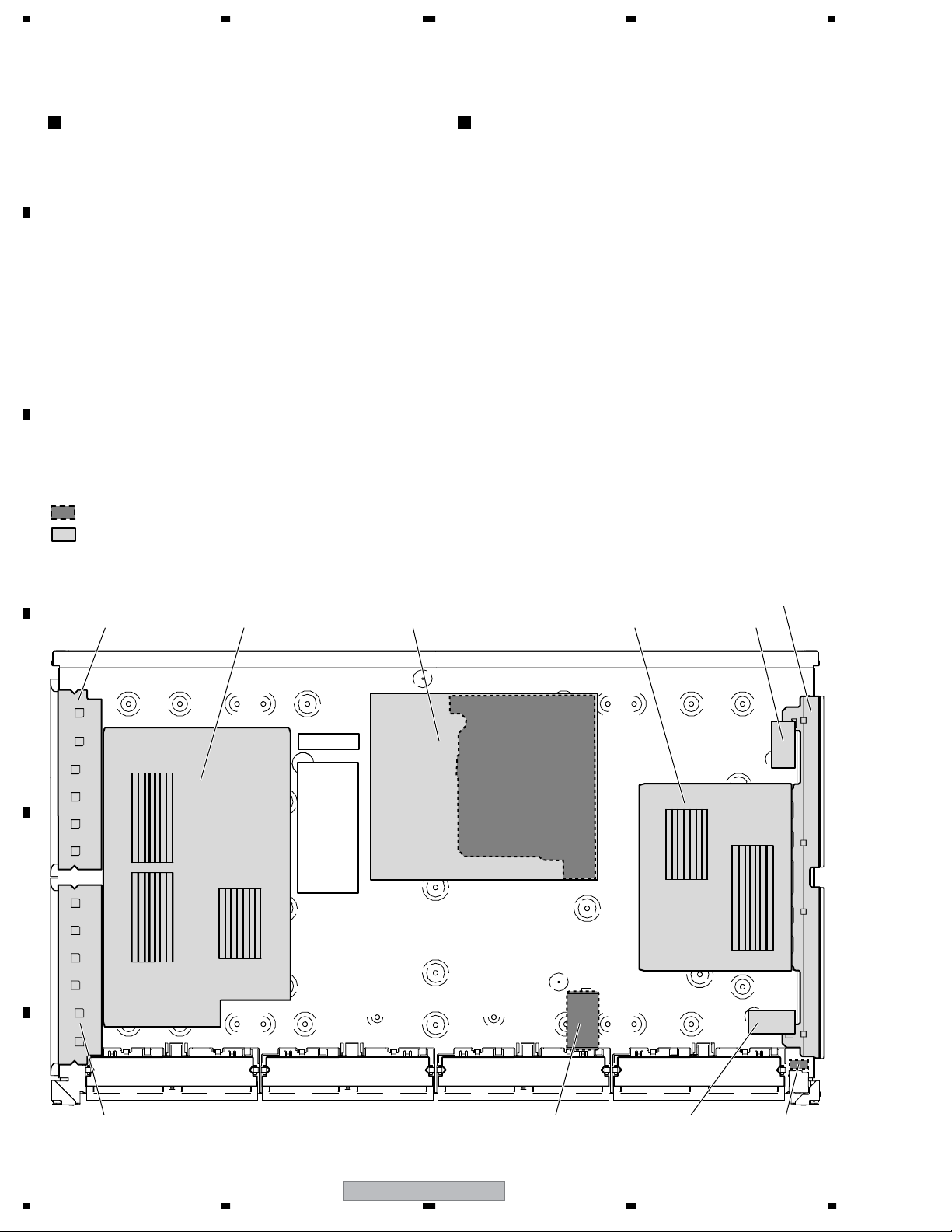
B
1. Power cord
2. AC inlet
3. Power switch (S1)
4. Fuse (In the POWER SUPPLY Unit)
5. STB transformer and Converter transformer
(In the POWER SUPPLY Unit)
6. Other primary side of the POWER SUPPLY Unit
C
: Part is Charged Section.
: Part is the High Voltage Generating Points
other than the Charged Section.
42 SCAN B Assy
42 Y DRIVE Assy 42 X DRIVE Assy SUS CLAMP 1 AssyPOWER SUPPLY Unit
The places where voltage is 100 V or more except for the charged
places described above. If the places are touched, there is a risk of
electric shock.
The VSUS voltage remains for several minutes after the power to
the unit is turned off. These places must not be touched until
about 10 minutes after the power is turned off, or it is confirmed
with a tester that there is no residual VSUS voltage.
If the procedures described in “10.3 POWER ON/OFF
FUNCTION FOR THE LARGE-SIGNAL SYSTEM” are
performed before the power is turned off, the voltage will be
discharged in about 30 seconds.
POWER SUPPLY Unit........................................................(205 V)
42 X DRIVE Assy...............................................(–180 V to 205 V)
42 Y DRIVE Assy...............................................................(500 V)
42 SCAN A Assy............................................................... (500 V)
42 SCAN B Assy............................................................... (500 V)
SUS CLAMP 1 Assy...........................................(–180 V to 205 V)
SUS CLAMP 2 Assy...........................................(–180 V to 205 V)
Conductive plate X
D
E
F
AC inlet Power switch (S1)42 SCAN A Assy
SUS CLAMP 2 Assy
Fig. High Voltage Generating Point (Rear view)
4
1234
PDP-427XD
5678
[Important Check Points for Good Servicing]
In this manual, procedures that must be performed during repairs are marked with the below symbol.
Please be sure to confirm and follow these procedures.
1. Product safety
Please conform to product regulations (such as safety and radiation regulations), and maintain a safe servicing environment by
following the safety instructions described in this manual.
1 Use specified parts for repair.
Use genuine parts. Be sure to use important parts for safety.
2 Do not perform modifications without proper instructions.
Please follow the specified safety methods when modification(addition/change of parts) is required due to interferences such as
radio/TV interference and foreign noise.
3 Make sure the soldering of repaired locations is properly performed.
When you solder while repairing, please be sure that there are no cold solder and other debris.
Soldering should be finished with the proper quantity. (Refer to the example)
4 Make sure the screws are tightly fastened.
Please be sure that all screws are fastened, and that there are no loose screws.
5 Make sure each connectors are correctly inserted.
Please be sure that all connectors are inserted, and that there are no imperfect insertion.
6 Make sure the wiring cables are set to their original state.
Please replace the wiring and cables to the original state after repairs.
In addition, be sure that there are no pinched wires, etc.
7 Make sure screws and soldering scraps do not remain inside the product.
Please check that neither solder debris nor screws remain inside the product.
8 There should be no semi-broken wires, scratches, melting, etc. on the coating of the power cord.
Damaged power cords may lead to fire accidents, so please be sure that there are no damages.
If you find a damaged power cord, please exchange it with a suitable one.
9 There should be no spark traces or similar marks on the power plug.
When spark traces or similar marks are found on the power supply plug, please check the connection and advise on secure
connections and suitable usage. Please exchange the power cord if necessary.
0 Safe environment should be secured during servicing.
When you perform repairs, please pay attention to static electricity, furniture, household articles, etc. in order to prevent injuries.
Please pay attention to your surroundings and repair safely.
A
B
C
D
2. Adjustments
To keep the original performance of the products, optimum adjustments and confirmation of characteristics within specification.
Adjustments should be performed in accordance with the procedures/instructions described in this manual.
3. Lubricants, Glues, and Replacement parts
Use grease and adhesives that are equal to the specified substance.
Make sure the proper amount is applied.
4. Cleaning
For parts that require cleaning, such as optical pickups, tape deck heads, lenses and mirrors used in projection monitors, proper
cleaning should be performed to restore their performances.
5. Shipping mode and Shipping screws
To protect products from damages or failures during transit, the shipping mode should be set or the shipping screws should be
installed before shipment. Please be sure to follow this method especially if it is specified in this manual.
56
PDP-427XD
E
F
5
7
8
1234
1.2 QUICK REFERENCE UPON SERVICE VISIT
A
Notes, PD/SD diagnosis, and methods for various settings
Notes when visiting for service
1. Notes when disassembling/reassembling
1 Rear case
When reassembling the rear case, the screws must be tightened in a
specific order. Be careful not to tighten them in the wrong order forcibly.
For details, see "Rear Case" in "6. DISASSEMBLY"
2 Attaching screws for the HDMI connector
When attaching the HDMI connector after replacing the Main Assy,
secure the HDMI connector manually with a screwdriver, but not
with an electric screwdriver. If you tighten the screws too tightly
with an electric screwdriver, the screw heads may be damaged, in
B
C
which case the screws cannot be untightened/tightened any more.
2. On parts replacement
1 How to discharge before replacing the Assys
A charge of significant voltage remains in the Plasma Panel even
after the power is turned off. Safely discharge the panel before
replacement of parts, in either manner indicated below:
Let the panel sit at least for 3 minutes after the power is turned off.
A:
B: Turn the Large Signal System off before the power is turned off
then, after 1 minute, turn the power off.
For details, see "10.2 Power ON/OFF Function for the Large-Signal
System."
2 On the settings after replacement of the Assys
Some boards need settings made after replacement of the Assys.
For details, see "7. ADJUSTMENT"
3. On various settings
1 SR+
After a repair using a PC, be sure to restore the setting for the
RS-232C connector to SR+.
2 Setting in Factory mode
After a Mask indication into the panel is performed, be sure to
set the Mask setting to "OFF" then exit Factory mode.
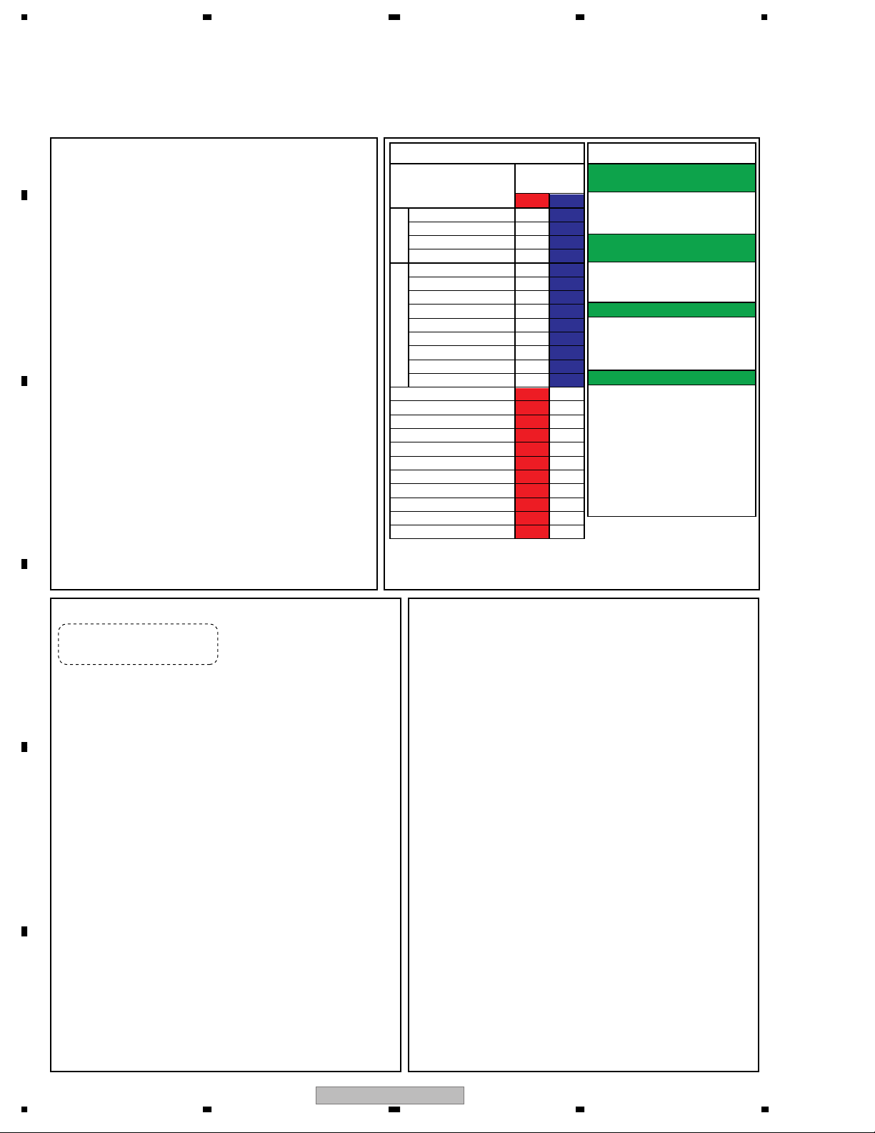
Quick Reference upon Service Visit 1
PD/SD
Item
Communication with the panel drive IC
Communication with the module IIC
DIGTAL-RST2
Panel high temperature
Panel section
Audio
Communication with the Module microcomputer
Main 3-wire serial communication
Main IIC communication
Communication with the Main microcomputer
FAN
Main section
Unit high temperature
Communication with the D-TUNER
MTB-RST2/RST4
POWER
SCAN
SCN-5V
Y-DRIVE
Y-DCDC
Y-SUS
ADRS
X-DRIVE
X-DCDC
X-SUS
UNKNOWN
No. of LEDs
flashing
Red Blue
Blue 1
Blue 2
Blue 3
Blue 4
Blue 5
Blue 6
Blue 7
Blue 8
Blue 9
Blue 10
Blue 11
Blue 12
Blue 13
Red 2
Red 3
Red 4
Red 5
Red 6
Red 7
Red 8
Red 9
Red 10
Red 11
Red 15
Change of settings
How to enter Factory mode using
the supplied remote control unit
In the same way as with the remote
control unit supplied with the 6thgeneration model
How to enter Integrator mode using
the supplied remote control unit
1 Enter the Standby mode.
2 Press [MENU].
3 Press [TV ].
How to switch UART 1 (Integrator)
1 Enter the Integrator mode.
2 Display "OFF" using [\].
3 Change the communication speed
using [«], then [\].
How to switch UART 2 (During Standby)
1 Enter the Standby mode.
2
Hold [VOL +] or [VOL -] pressed for 3 seconds.
3
Hold [SPLIT] pressed for 3 seconds.
4-1 To set to 232C, press [ENTER].
5-2
To set to SR+, press [HOME MENU].
Note:
If switching is completed successfully,
the red LED will flash twice.
Note 1:
Use a remote control unit supplied with
the 6th-generation models or later.
Note 2:
Do not hold a key pressed for more
than 5 seconds.
How to locate several items on the Factory menu
{ } : Item on the Factory menu
[ ] : Key on the remote control unit
D
E
F
" " : Screen indication
1. Confirmation of accumulated power-on time and power-on
count
Select {INFORMATION} then {HOUR METER}.
(After entering Factory mode, press [«] four times.)
2. Confirmation of the Power-down and Shutdown histories
1 Panel system
PD: Select {PANEL FACTORY} then {POWER DOWN}.
(After entering Factory mode, press [MUTING] once, press
[ENTER], then press [«] three times.)
SD: Select {PANEL FACTORY} then {SHUT DOWN}.
(After entering Factory mode, press [MUTING] once, press
[ENTER], then press [«] four times.)
2 Main Assy
Select {INFORMATION} then {MAIN NG}.
(After entering Factory mode, press [«] three times.)
3. How to display the Mask indication
1 Mask indication in the panel side
1. Select {PANEL FACTORY} then {RASTER MASK SETUP}.
(After entering Factory mode, press [MUTING] once, press [ENTER],
then press [«] 8 times.)
2. Press [ENTER], then select a Mask indication, using [»] or [«].
2 Mask (SG screen) indication in the Main Assy (MAIN VDEC)
1. Select either Input 1 or 2, to which no signal is input (
2. Select {INITIALIZE} then {SG MODE}. Press [|]. (After entering
Factory mode, press [MUTING] three times, then press [«] once.)
Then, the indication at the lower right of the screen changes from
"OFF" to "ANA AD YCBCR".
3. You can change Mask patterns by pressing [«] to select {SG
PATTERN} then using [|] or [\].
Note: When you switch "SG MODE" routes, some displays become
monochrome, as they are in Y-signal only mode.
black screen
Adjustments and Settings after replacement of the
Assys (Procedures in Factory mode)
1. Digital Video Assy: Transfer of backup data
1 Select {PANEL FACTORY}, {ETC}, then {BACKUP DATA}. (After entering Factory
mode, press [MUTING] once, press [ENTER], press [«] seven times, then press
[ENTER].)
2 Select {TRANSFER}, using [\], then hold [SET] pressed for at least 5 seconds.
3 After transfer of backup data is completed, {ETC} is automatically selected, and the
LED on the front panel returns to normal lighting.
2. MAIN Assy : Switching to SR+ from RS-232C
1 Enter the Integrator mode. (The way is described above.)
2 As SR+ <=> is [OFF] state, switch to [ON] state by using [\].
3 Tu rn the POWER switch of the main unit off by the remote control.
3. POWER SUPPLY Unit: Clearance of the accumulated power-on count
and maximum temperature value
1 Select {PANEL FACTORY}, {ETC}, then {P COUNT INFO}. (After entering Factory
mode, press [MUTING] once, press [ENTER], press [«] seven times, press [ENTER],
then press [«] six times.)
2 Press [\] to select "CLEAR". Hold [SET] pressed for at least 5 seconds.
After clearance is completed, "ETC" is automatically selected. Clear the maximum
temperature value (MAX TEMP) in the same manner.
4. Other Assys: Clearance of the maximum temperature value
1 Select {PANEL FACTORY}, {ETC}, then {MAX TEMP}. (After entering Factory mode,
press [MUTING] once, press [ENTER], press [«] seven times, press [ENTER], then
press [«] seven times.)
2 Press [\] to select "CLEAR". Hold [SET] pressed for at least 5 seconds.
After clearance is completed, "ETC" is automatically selected.
).
6
PDP-427XD
1234
5678
Quick Reference upon Service Visit 2
Mode transition and structure of layers in Service Factory mode
Mode transition in Service Factory mode
Enter
INFORMATION mode
1. VERSION (1)
2. VERSION (2)
3. MAIN NG
4. TEMPERATURE
5. HOUR METER
6. HDMI SIGNAL INFO1
7. HDMI SIGNAL INFO2
8. VDEC SIGNAL INFO
PANEL FACTORY mode
1. PANEL INFORMATION
2. PANEL WORKS
3. POWER DOWN
4. SHUT DOWN
5. PANEL-1 ADJ
6. PANEL-2 ADJ
7. PANEL REVICE
8. ETC.
9. RASTER MASK SETUP
10. PATTEN MASK SETUP
11. COMBI MASK SETUP
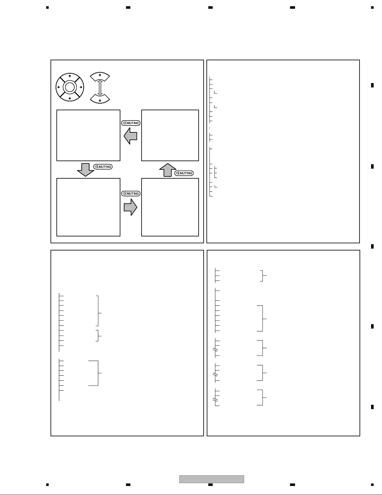
Up
Down
• To shift to another mode, press [MUTING].
• To shift to another item in a specific mode,
press [»] or [«].
• To shift to the next nested layer below for an
item with a "(+)" indication, press [ENTER].
To return to the next nested layer above,
also press [ENTER].
INITIALIZE mode
1. SYNC DET
2. SG MODE
3. SG PATTERN
4. SIDE MASK LEVEL
5. FINAL SETUP
6. CVT AUTO
7. HDMI INTR POSITION
OPTION mode
1. EDID WRITE MODE
2. CH PRESET
Structure of Layers in Service Factory Mode
INFORMATION mode
1. VERSION (1) Flash Versions for PANEL system and MAIN system
2. VERSION (2) Flash Versions for DTV system
3. MAIN NG SD histories for MAIN (Going Clear model by SET key)
3-1. CLEAR Select Yes by [\] key \ pushing and hold [SET] key
4. TEMPERATURE TEMP 1, TEMP2 and FAN mode are displayed
5. HOUR METER Hour meter and number of Power ON are displayed
5-1. CLEAR Select Yes by [\] key \ pushing and hold [SET] key
6. HDMI SIGNAL INFO 1 For factory use
7. HDMI SIGNAL INFO 2 Signal info of HDMI are displayed ( Detail are on SM )
8. VDEC SIGNAL INFO For factory use
PANEL FACTORY mode Refer to [PANEL FACTORY MODE]
OPTION
1. EDID WRITE MODE For factory use
2. CH PRESET For production line use
INITIALIZE
1. SYNC DET (+) For factory use
2. SG MODE SG signal from MAIN VDEC (
3. SG PATTERN For factory use
4. SIDE MASK LEVEL(+) For factory use
4-1. R MASK LEVEL
4-2. G MASK LEVEL
4-3. B MASK LEVEL
5. FINAL SETUP Set to Factory default settings (it should perform after
5-1. DATA RESET replacing a MAIN board )
6. CVT AUTO For factory use
7. HDMI INTR POSITION(+) For factory use
Composite signal is required
A
B
)
C
Structure of Layers in Panel Factory Mode 1
1. PANEL INFORMATION Version indication of the panel
2. PANEL WORKS Indications of the accumulated power-on time, pulse-meter
3. POWER DOWN Indication of the Power-down history
4. SHUT DOWN Indication of the Shutdown history
5. PANEL-1 ADJ (+)
1. X-SUS B
2. Y-SUS B
3. Y-SUSTAIL T1
4. Y-SUSTAIL T2 Modification not required because these items are basically
5. Y-SUSTAIL W for factory presetting
6. XY-RST W1
7. XY-RST W2
8. VOL SUS
9. VOL OFFSET Settings required after replacement of the panel
10. VOL RST P
11. SUS FREQ. For AM noise prevention (Depending on the mode,
6. PANEL-2 ADJ (+)
1. R-HIGH
2. G-HIGH
3 .B-HIGH Parameters for the WB adjustment of the panel, which are
4. R-LOW required during adjustment after panel replacement
5. G-LOW
6. B-LOW
7. ABL Setting of the power consumption. A setting table is
To "Structure of Layers in Panel Factory Mode 2"
count, and power-on count of the panel
brightness of the screen changes.)
available for each vertical signal.
Structure of Layers in Panel Factory Mode 2
7. PANEL REVISE (+)
R-LEVEL
G-LEVEL Items for use by engineers
B-LEVEL
8. ETC (+)
1. BACKUP DATA For transferring backup data (after replacement of
2. DIGITAL EEPROM To clear data of the digital video
3. PD INFO.
4. SD INFO. For clearance of data for the corresponding items.
5. HR-MTR INFO. The clearing method is the same: Select "CLEAR",
6. PM/B1-B5 using [\], then hold [SET] pressed for at least 5
7. P COUNT INFO. seconds. After clearance is completed, {ETC} is
8. MAX TEMP. automatically selected.
9. RASTER MASK SETUP (+)
1. MASK OFF
2. RST MASK 01 For use while Raster Mask (full mask) is displayed.
• • • • • Use [»] or [«] to select the type of mask.
25. RST MASK 24
10. PATTEN MASK SETUP (+)
1. MASK OFF
2. PTN MASK 01 For use while Pattern Mask is displayed. Use [»] or
• • • • • [«] to select the type of mask.
40. PTN MASK 39
11. COMBI MASK SETUP (+)
1. MASK OFF
2. CMB MASK 01 For use while Combination Mask is displayed.
• • • • • Use [»] or [«] to select the type of mask.
11. CMB MASK 10
the DIGITAL Assy)
D
E
56
PDP-427XD
F
7
7
8

1234
1.3 JIGS LIST
A
Cleaning
Name Part No. Remarks
Cleaning liquid GEM1004
Cleaning paper GED-008
Used to fan cleaning.
Refer to "2.4 CHASSIS SECTION (1/2).
CONTENTS
1. NOTES ON SERVICE VISIT.........................................................................................................................................2
B
C
D
E
F
1.1 SAFETY INFORMATION .......................................................................................................................................2
1.2 QUICK REFERENCE UPON SERVICE VISIT.......................................................................................................6
1.3 JIGS LIST ..............................................................................................................................................................8
2. EXPLODED VIEWS AND PARTS LIST ......................................................................................................................10
2.1 PACKING SECTION ............................................................................................................................................10
2.2 REAR SECTION ..................................................................................................................................................12
2.3 FRONT SECTION................................................................................................................................................14
2.4 CHASSIS SECTION (1/2)....................................................................................................................................16
2.5 CHASSIS SECTION (2/2)....................................................................................................................................18
2.6 PANEL CHASSIS SECTION................................................................................................................................20
2.7 MULTI BASE SECTION .......................................................................................................................................22
2.8 PDP SERVICE PANEL ASSY 427 (AWU1208) ...................................................................................................24
2.9 TABLE TOP STAND (PDP-4270XD and PDP-4270XA ONLY).............................................................................25
3. PCB PARTS LIST .......................................................................................................................................................26
4. BLOCK DIAGRAM AND SCHEMATIC DIAGRAM......................................................................................................42
4.1 OVERALL WIRING DIAGRAM (1/2) ....................................................................................................................42
4.2 OVERALL WIRING DIAGRAM (2/2) ....................................................................................................................44
4.3 OVERALL BLOCK DIAGRAM (1/2) .....................................................................................................................46
4.4 OVERALL BLOCK DIAGRAM (2/2) .....................................................................................................................48
4.5 POWER SUPPLY UNIT........................................................................................................................................49
4.6 42 X DRIVE, SUS CLAMP 1 and SUS CLAMP 2 ASSYS ...................................................................................50
4.7 42 Y DRIVE ASSY ...............................................................................................................................................51
4.8 POWER SUPPLY BLOCK of 42 X DRIVE and 42 Y DRIVE ASSYS...................................................................52
4.9 42 SCAN A and 42 SCAN B ASSYS ...................................................................................................................53
4.10 42 ADDRESS ASSY ..........................................................................................................................................54
4.11 42 DIGITAL ASSY..............................................................................................................................................55
4.12 SIGNAL BLOCK DIAGRAM...............................................................................................................................56
4.13 R07 DT ASSY (PDP-4270XD and PDP-427XD ONLY) .....................................................................................58
4.14 POWER SUPPLY BLOCK of MAIN ASSY .........................................................................................................59
4.15 42E AUDIO ASSY..............................................................................................................................................60
4.16 POWER SUPPLY BLOCK of 42E AUDIO, LED IR and SIDE KEY ASSYS.......................................................61
4.17 VOLTAGES.........................................................................................................................................................62
4.18 WAVEFORMS ....................................................................................................................................................70
5. DIAGNOSIS ................................................................................................................................................................74
5.1 TROUBLE SHOOTING ........................................................................................................................................74
5.1.1 FLOWCHART OF FAILURE ANALYSIS FOR THE WHOLE UNIT................................................................74
5.1.2 FLOWCHART OF FAILURE ANALYSIS FOR THE POWER SUPPLY UNIT.................................................76
5.1.3 FLOWCHART OF FAILURE ANALYSIS FOR THE DIGITAL ASSY ..............................................................77
5.1.4 FLOWCHART OF FAILURE ANALYSIS FOR THE DRIVE ASSY.................................................................78
5.1.5 FLOWCHART OF FAILURE ANALYSIS FOR THE MAIN ASSY...................................................................82
5.1.6 FLOWCHART OF FAILURE ANALYSIS FOR THE VIDEO SYSTEM............................................................83
5.1.7 FLOWCHART OF FAILURE ANALYSIS FOR THE AUDIO SYSTEM ...........................................................90
5.2 DIAGNOSIS OF PD (POWER-DOWN)................................................................................................................93
5.2.1 BLOCK DIAGRAM OF THE POWER-DOWN SIGNAL..................................................................................93
5.2.2 DIAGNOSIS OF THE PD (POWER-DOWN) .................................................................................................94
5.3 DIAGNOSIS OF SD (SHUTDOWN).....................................................................................................................97
5.3.1 BLOCK DIAGRAM OF THE SHUTDOWN SIGNAL.......................................................................................97
5.3.2 SD (SHUTDOWN) DIAGNOSIS ....................................................................................................................98
5.4 INFORMATION ON SYMPTOMS THAT DO NOT CONSTITUTE FAILURE........................................................99
6. DISASSEMBLY.........................................................................................................................................................100
6.1 PCB LOCATION.................................................................................................................................................100
8
1234
PDP-427XD

5678
6.2 DISASSEMBLY .................................................................................................................................................. 101
7. ADJUSTMENT ......................................................................................................................................................... 107
7.1 ADJUSTMENT REQUIRED WHEN THE SET IS REPAIRED OR REPLACED.................................................107
7.2 ADJUSTMENT REQUIRED WHEN PART IS REPLACED................................................................................108
7.3 BACKUP WHEN THE PANEL UNIT IS ADJUSTED.......................................................................................... 109
A
7.4 HOW TO CLEAR HISTORY DATA.....................................................................................................................112
7.5 ADJUSTMENT WHEN THE SERVICE PANEL ASSY IS REPLACED ..............................................................113
8. SERVICE FACTORY MODE .................................................................................................................................... 115
8.1 OUTLINE OF THE SERVICE FACTORY...........................................................................................................115
8.1.1 SERVICE FACTORY MODE TRANSITION CHART....................................................................................115
8.1.2 HOW TO ENTER/EXIT SERVICE FACTORY MODE.................................................................................. 115
8.1.3 OPERATION OF SERVICE FACTORY MODE............................................................................................115
8.1.4 REMOTE COTROL CODE..........................................................................................................................116
8.1.5 FACTORY HIERARCHICAL TABLE ............................................................................................................117
8.1.6 INDICATIONS IN SERVICE FACTORY MODE...........................................................................................118
8.2 FACTORY MENU...............................................................................................................................................120
8.2.1 INFORMATION............................................................................................................................................120
B
8.2.2 PANEL FACTORY .......................................................................................................................................128
8.2.3 OPTION.......................................................................................................................................................138
8.2.4 INITIALIZE...................................................................................................................................................138
9. RS-232C ..................................................................................................................................................................141
9.1 OUTLINE OF RS-232C COMMAND .................................................................................................................141
9.1.1 PREPARED TOOLS ....................................................................................................................................141
9.1.2 USING RS-232C COMMANDS................................................................................................................... 141
9.1.3 COMMAND PROTOCOL.............................................................................................................................142
9.1.4 COMMAND DEFINITION............................................................................................................................143
9.2 LIST OF RS-232C COMMANDS.......................................................................................................................145
9.3 OUTLINE OF EACH COMMANDS.................................................................................................................... 151
9.3.1 ACQUISITION OF PANEL STATUS • • • [QS1] ...........................................................................................151
C
9.3.2 ACQUISITION OF PANEL OPERATION DATA • • • [QS2] .......................................................................... 152
9.3.3 ACQUISITION OF OTHER DATA ON THE PANEL • • • [QIP] .....................................................................153
9.3.4 ACQUISITION OF PANEL ADJUSTMENT DATA (COMMON DATA) • • • [QAJ] .........................................153
9.3.5 ACQUISITION OF ABL/WB ADJUSTMENT DATA • • • [QPW] ...................................................................154
9.3.6 ACQUISITION OF PULSE METER VALUE • • • [QPM] ..............................................................................154
9.3.7 ACQUISITION OF PD LOGS • • • [QPD].....................................................................................................155
9.3.8 ACQUISITION OF SD LOGS • • • [QSD].....................................................................................................156
9.3.9 QS6 .............................................................................................................................................................157
9.3.10 QMT ..........................................................................................................................................................157
9.3.11 QNG ..........................................................................................................................................................158
9.3.12 DRV........................................................................................................................................................... 159
9.3.13 OTHER COMMANDS ...............................................................................................................................160
D
10. GENERAL INFORMATION ....................................................................................................................................161
10.1 POWER ON SEQUENCE................................................................................................................................161
10.2 POWER SUPPLY TRANSITION STATUS........................................................................................................164
10.3 POWER ON/OFF FUNCTION FOR THE LARGE-SIGNAL SYSTEM .............................................................165
10.4 LED INFORMATION........................................................................................................................................166
10.5 SPECIFICATION ABOUT THE THERMAL PROTECTION..............................................................................167
10.6 PROCESSING IN ABNORMALITY .................................................................................................................168
11. SPECIFICATIONS.................................................................................................................................................. 170
11.1 SPECIFICATIONS ...........................................................................................................................................170
11.2 ACCESSORIES............................................................................................................................................... 171
11.3 PANEL FACILITIES..........................................................................................................................................172
E
11.3.1 PDP-427XD, PDP-4270XD .......................................................................................................................172
11.3.2 PDP-427XA, PDP-4270XA........................................................................................................................177
12. IC INFORMATION ..................................................................................................................................................182
56
PDP-427XD
F
9
7
8
1234
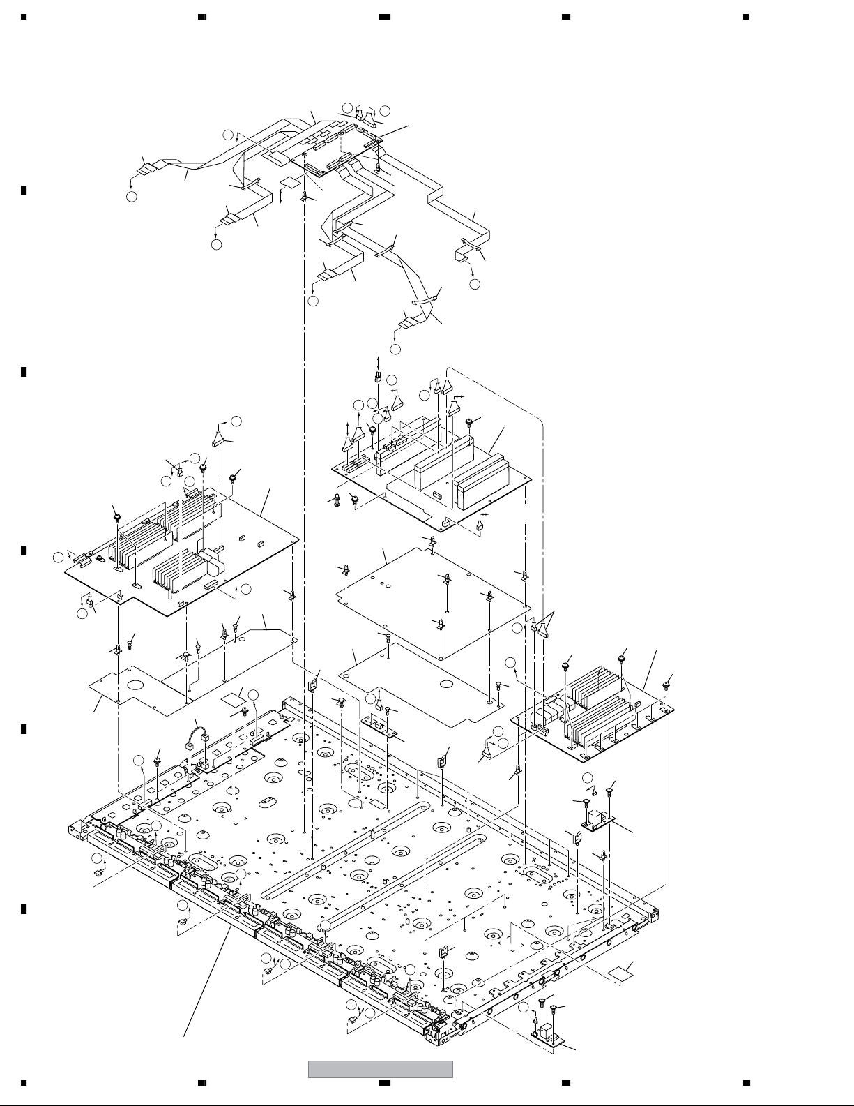
2. EXPLODED VIEWS AND PARTS LIST
NOTES:
Parts marked by "NSP" are generally unavailable because they are not in our Master Spare Parts List.
The mark found on some component parts indicates the importance of the safety factor of the part.
A
Therefore, when replacing, be sure to use parts of identical designation.
Screws adjacent to mark on product are used for disassembly.
For the applying amount of lubricants or glue, follow the instructions in this manual.
(In the case of no amount instructions, apply as you think it appropriate.)
2.1 PACKING SECTION
B
C
20
19
24
D
E
9
Ferrite core
Cable tie
18
PDP-4270XD/WYVIXK5, PDP-427XD/WYVIXK5,
PDP-427XA/WYVIXK5, WYV5
only
5
7
6
Speed clamp ×3
8
Bead band ×3
WYVIXK5 model
only
16
10
PDP-4270XD,
PDP-4270XA only
11
14
12
4
25
2
1
21
22
3
15
13
17
Tabletop Stand bundle
16
F
10
1234
PDP-427XD
23
PDP-4270XD, PDP4270XA model only
>
>
5678
(1) PACKING SECTION PARTS LIST
No. Description Part No.
Mark
1Power Cord (2 m) ADG1214
2Power Cord Lid See Contrast table (2)
3 Remote Control Unit See Contrast table (2)
4 Battery Cover See Contrast table (2)
5 Operating Instructions See Contrast table (2)
(Italian,Dutch,Spanish)
6 Operating Instructions See Contrast table (2)
(English,French,German)
7 Block Diagram See Contrast table (2)
NSP 8 Dry Cell Battery (R06, AA) VEM1031
9Ferrite Core (L5321) ATX1039
10 Binder Assy AEC1908
NSP 11 Hexagonal Wrench (6 mm) See Contrast table (2)
12 Cleaning Cloth AED1285
13 Caution Card See Contrast table (2)
14 Cleaning Caution See Contrast table (2)
No. Description Part No.
Mark
NSP 15 Warranty Card ARY1114
16 Polyethylene Bag AHG1340
17 Polyethylene Bag AHG1326
18 Polyethylene Bag AHG1337
19 Pad (427 T-L) See Contrast table (2)
20 Pad (427 T-R) See Contrast table (2)
21 Pad (427 B-L) See Contrast table (2)
22 Pad (427 B-R) See Contrast table (2)
23 Under Carton (427) See Contrast table (2)
24 Upper Carton See Contrast table (2)
25 Mirror Mat See Contrast table (2)
A
B
(2) CONTRAST TABLE
PDP-427XD/WYVIXK5, PDP-4270XD/WYVIXK5, PDP-4270XA/WYVIXK5, WYV5, PDP-427XA/WYVIXK5 and
WYV5 are constructed the same except for the following:
Mark No. Symbol and Description
2Power Cord Lid AHC1087 AHC1087 AHC1087 AHC1087 AHC1085 AHC1085
3 Remote Control Unit AXD1532
4 Battery Cover AZA7626 AZA7424 AZA7424 AZN2626 AZA7424 AZN2626
5 Operating Instructions
(Italian,Dutch,Spanish)
6 Operating Instructions
(English,French,German)
7 Block Diagram ARY1189 ARY1189 ARY1189 ARY1189 Not used Not used
NSP 11 Hexagonal Wrench (6 mm) Not used
13 Caution Card ARM1310 ARM1310 ARM1310 ARM1310 ARM1232 ARM1232
14 Cleaning Caution PTK ARM1311 ARM1311 ARM1311 ARM1311 Not used Not used
14 Wiping Cloth Caution Not used Not used Not used Not used ARM1283 ARM1283
PDP-427XD
/WYVIXK5
ARC1562 ARC1565 Not used ARC1564 Not used ARC1563
ARE1428 ARE1431 ARE1433 ARE1430 ARE1432 ARE1429
PDP-4270XD
/WYVIXK5
AXD1515
AEF1029
PDP-4270XA
/WYVIXK5
AXD1541 AXD1540 AXD1541 AXD1540
AEF1029 Not used AEF1029 Not used
PDP-427XA
/WYVIXK5
PDP-4270XA
/WYV5
PDP-427XA
/WYV5
C
D
E
19 Pad (427 T-L) AHA2554 AHA2554 AHA2554 AHA2554 AHA2534 AHA2534
20 Pad (427 T-R) AHA2555 AHA2555 AHA2555 AHA2555 AHA2535 AHA2535
21 Pad (427 B-L) AHA2600 AHA2600 AHA2600 AHA2600 AHA2592 AHA2592
22 Pad (427 B-R) AHA2601 AHA2601 AHA2601 AHA2601 AHA2593 AHA2593
23 Under Carton (427) AHD3496 AHD3496 AHD3496 AHD3496 AHD3471 AHD3471
24 Upper Carton AHD3515 AHD3514 AHD3497 AHD3517 AHD3513 AHD3516
25 Mirror Mat AHG1327 AHG1327 AHG1327 AHG1327 AHG1284 AHG1284
PDP-427XD
56
7
8
F
11
1234
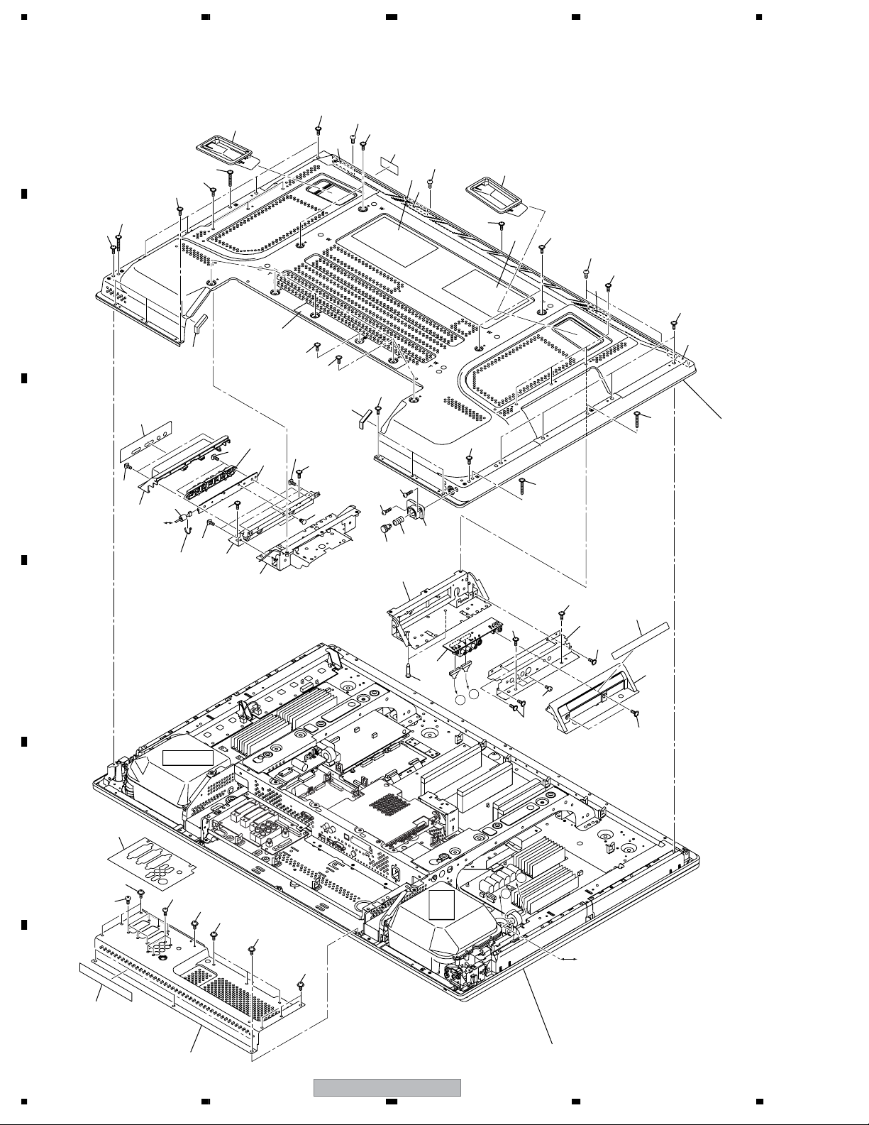
2.2 REAR SECTION
A
12
29
33
33
29
33
37
31
33
8
16
13
31
12
8
37
15
33
31
33
B
8
37
11
18
30
8
33
33
11
25
24
34
C
33
3
22
MAIN
CN4010
(Accessory of No.3)
Binder
35
33
5
33
1
35
32
10
7
32
17
6
14
28
33
29
29
27
35
35
D
4
2
26
33
23
9
A
B
33
36
33
36
20
33
36
B
A
33
E
33
35
TANSHI
33
F
19
21
12
1234
PDP-427XD
CN9001, CN9002
Refer to
"2.3 FRONT SECTION".
5678
(1) REAR SECTION PARTS LIST
No. Description Part No.
Mark
1 SIDE KEY Assy AWW1133
2 SIDE Assy AWW1162
3 Filter CTX1054
4 Side Input Panel (E) ANC2418
5 Function Button Base ANG2923
No. Description Part No.
Mark
21 Terminal Panel B See Contrast table (2)
22 Function Button Panel AMB2906
23 Side Input Cover AMB2911
24 Function Button (E) AAC1565
25 Function Button Sheet (E) AAK2896
A
6 Side Input Shield ANK1834
7 Function Button Shield ANK1835
8 Rear Case Cushion AEB1439
NSP 9 PCB Support AEC1288
10 Locking Card Spacer AEC2019
11 Protection Sheet C AED1300
12 Inner Grip Assy AMR3434
NSP 13 Name Label See Contrast table (2)
14 Coil Spring ABH1125
15 Bolt Caution Label See Contrast table (2)
16 Serial Seal AAX3143
17 Power Button AAD4145
18 Terminal Label A See Contrast table (2)
19 Terminal Label C See Contrast table (2)
20 Terminal Label B See Contrast table (2)
26 Input Cover Label E See Contrast table (2)
27 Rear Case (427) ANE1655
28 Power Button Holder AMR3539
29 Screw (3 x 40P) ABA1332
30 Screw ABA1341
31 Screw (4 x 18) ABA1353
32 Screw BPZ30P140FTB
33 Screw AMZ30P060FTB
34 Screw AMZ30P080FTC
35 Screw APZ30P080FTB
36 Screw BPZ30P080FTB
37 Screw TBZ40P080FTB
B
C
(2) CONTRAST TABLE
PDP-427XD/WYVIXK5, PDP-4270XD/WYVIXK5, PDP-4270XA/WYVIXK5, WYV5, PDP-427XA/WYVIXK5 and
WYV5 are constructed the same except for the following:
Mark No. Symbol and Description
NSP 13 Name Label AAL2804 AAL2801 AAL2803 AAL2806 AAL2802 AAL2805
15 Bolt Caution Label AAX3005 AAX3005 AAX3005 AAX3005 Not used Not used
15 Caution Label Not used Not used Not used Not used AAX3117 AAX3117
18 Terminal Label A AAX3337 AAX3343 AAX3399 AAX3398 AAX3344 AAX3332
19 Terminal Label C AAX3339 AAX3340 AAX3340 AAX3339 AAX3340 AAX3339
20 Terminal Label B AAX3417 AAX3419 AAX3419 AAX3417 AAX3419 AAX3417
21 Terminal Panel B ANC2403 ANC2429 ANC2429 ANC2403 ANC2429 ANC2403
26 Input Cover Label E AAX3396 AAX3397 AAX3397 AAX3396 AAX3376 AAX3375
PDP-427XD
/WYVIXK5
PDP-4270XD
/WYVIXK5
PDP-4270XA
/WYVIXK5
PDP-427XA
/WYVIXK5
PDP-4270XA
/WYV5
PDP-427XA
/WYV5
D
E
F
56
PDP-427XD
13
7
8
1234
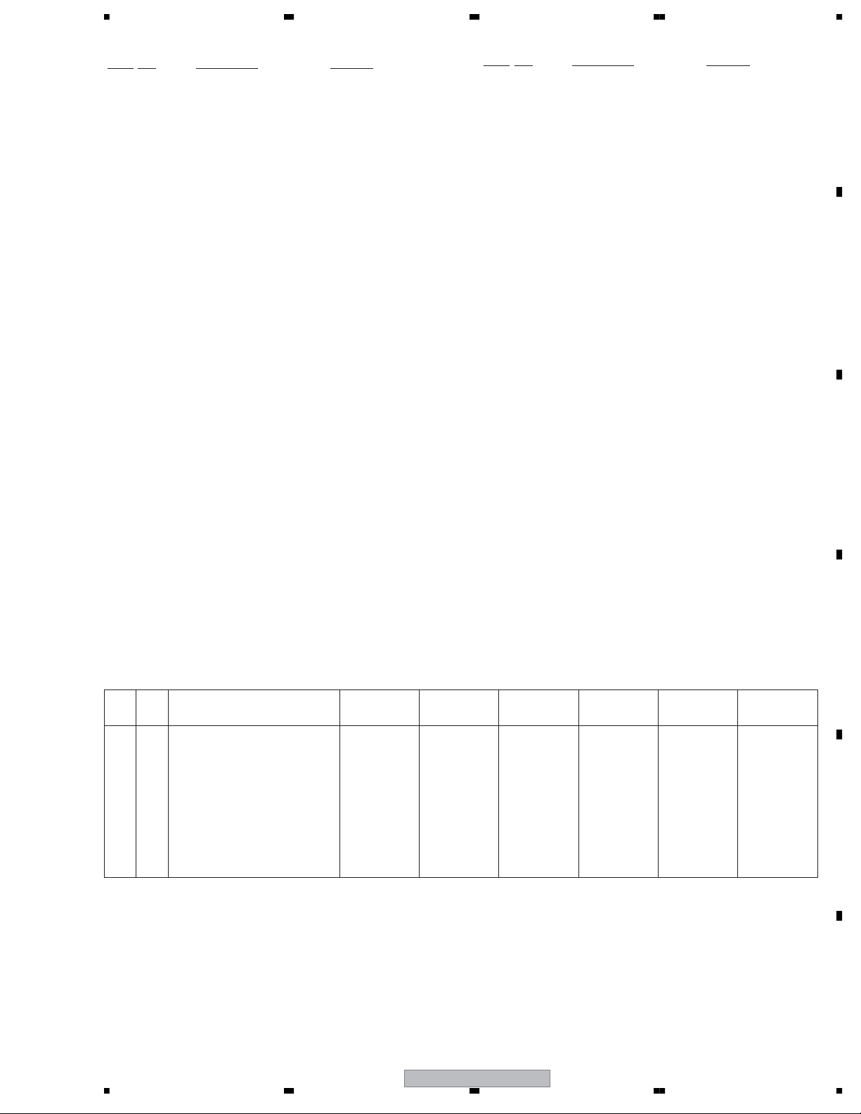
2.3 FRONT SECTION
A
PDP-4270XD/WYVIXK5
B
PDP-4270XA/WYVIXK5
PDP-4270XA/WYV5
Only stick here
Refer to
"2.4 CHASSIS SECTION (1/2)".
3
8
17
MAIN
CN4006
1
8
18
16
21
8
8
MAIN
2
6
5
CN4010
20
15
11
4
8
12
C
11
D
13
7
E
5
3
22
4
12
10
9
14
F
14
1234
PDP-427XD

5678
(1) FRONT SECTION PARTS LIST
No. Description Part No.
Mark
1 42 & 60 LED Assy AWW1134
2 LED IR Assy AWW1136
3 Blind Cushion (427HX) AEB1443
4 Speaker Cushion AEB1452
5 Speaker Cushion S See Contrast table (2)
6 Nyron Rivet AEC1671
7 Insulation Sheet B AED1284
8 Insulation Sheet See Contrast table (2)
9 Reinforcement Frame AMR3620
10 Front Case Assy See Contrast table (2)
A
11 Panel Cushion V (42) AED1301
12 Panel Cushion H (42) AED1309
13 Pioneer Name Plate AAM1096
14 Punching Sheet See Contrast table (2)
15 Front Collar AMR3541
16 Screw (3 x 30P) ABA1350
17 Screw (M3 x 4) ABA1354
18 Screw APZ30P080FTB
19 Front Case Cushion See Contrast table (2)
20 IR Block Cushion AEB1465
21 IR Blind Sheet AAX3455
22 Insulation Sheet B See Contrast table (2)
(2) CONTRAST TABLE
PDP-427XD/WYVIXK5, PDP-4270XD/WYVIXK5, PDP-4270XA/WYVIXK5, WYV5, PDP-427XA/WYVIXK5 and
WYV5 are constructed the same except for the following:
Mark No. Symbol and Description
5 Speaker Cushion S AEB1460 Not used Not used AEB1460 Not used AEB1460
8 Insulation Sheet AED1289 Not used Not used AED1289 Not used AED1289
10 Front Case Assy AMB2968 AMB2971 AMB2972 AMB2969 AMB2972 AMB2969
14 Punching Sheet AAS1014 AAS1015 AAS1015 AAS1014 AAS1015 AAS1014
19 Front Case Cushion (42B) AEB1462 AEB1464 AEB1464 AEB1462 AEB1464 AEB1462
PDP-427XD
/WYVIXK5
PDP-4270XD
/WYVIXK5
PDP-4270XA
/WYVIXK5
PDP-427XA
/WYVIXK5
PDP-4270XA
/WYV5
PDP-427XA
/WYV5
B
C
D
E
22 Insulation Sheet B AED1284 Not used Not used AED1284
PDP-427XD
56
7
Not used
AED1284
F
15
8
1234
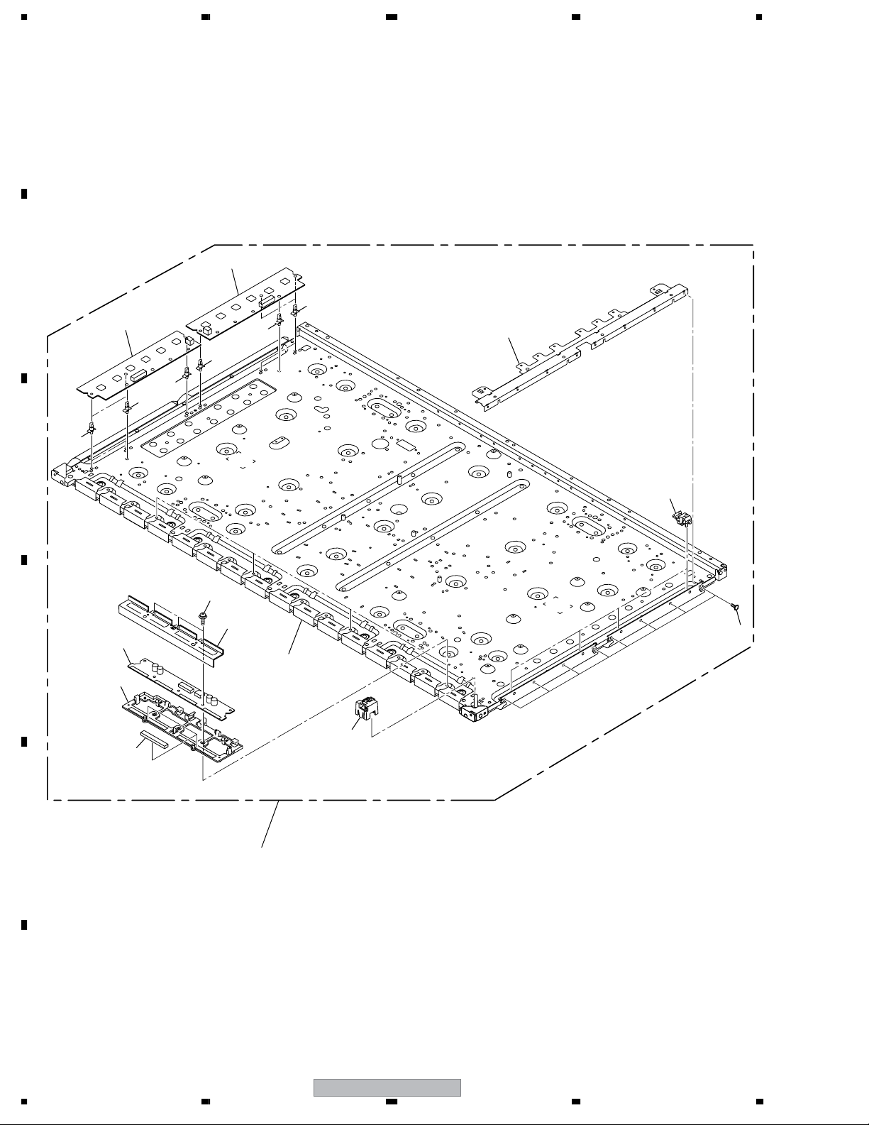
2.4 CHASSIS SECTION (1/2)
A
35
31
31
B
31
32
22
31
36
31
10
26
19
35
36
Refer to
"2.7 MULTI BASE SECTION".
35
36
31
11
35
31
31
31
31
30
42E AUDIO
30
31
CN3753
1
C
31
24
42E AUDIO
CN3753
30
29
14
24
29
13
D
30
32
23
29
7
16
31
30
16
30
27
30
15
35
19
34
3
POWER
12
P3
6
29
28
34
AC inlet
32
2
22
18
18
18
MAIN
CN4009
4
33
18
15
25
E
33
25
29
8
9
25
25
20
23
32
29
21
5
30
13
14
F
30
Refer to
"2.5 CHASSIS SECTION (2/2)".
16
PDP-427XD
1234

5678
CHASSIS SECTION (1/2) PARTS LIST
No. Description Part No.
Mark
1 Speaker Box Assy L AMW1010
2 Speaker Box Assy R AMW1011
3Power Switch (S1) ASG1092
4Fan Motor 80 x 25L AXM1059
5Ferrite Core ATX1044
6 Housing Wire (42, 50)(J103) ADX3320
7Front Chassis VL (427) AMA1020
8Front Chassis VR (427) AMA1021
9Front Chassis H Assy (427) ANA2047
10 Sub Frame Assy L (427) ANA1943
>
>
>
A
11 Sub Frame Assy R (427) ANA1944
12 Fan Holder ANG2833
13 Panel Holder V1 (427) ANG2920
14 Panel Holder V2 (427) ANG2921
15 Panel Holder H (427) ANG2922
16 Multi Base Holder ANG2937
17 • • • • •
18 Floating Rubber 80 AEB1427
19 Wire Saddle AEC1745
20 Ferrite Core Holder AEC1818
21 Flat Clamp AEC1879
22 Locking Wire Saddle AEC1948
23 Mini Clamp AEC2090
24 Re-use Wire Saddle AEC2091
25 Address Gasket (42) ANK1877
26 Gasket D ANK1840
27 Switch Holder AMR3540
28 Re-use Wire Saddle AEC1945
29 Screw ABA1351
30 Screw ABZ30P080FTC
B
C
D
31 Screw AMZ30P060FTB
32 Screw APZ30P080FTB
33 Screw BBZ30P060FTC
34 Screw BPZ30P080FTB
35 Screw TBZ40P080FTB
36 Screw ABA1364
56
PDP-427XD
E
F
17
7
8
1234
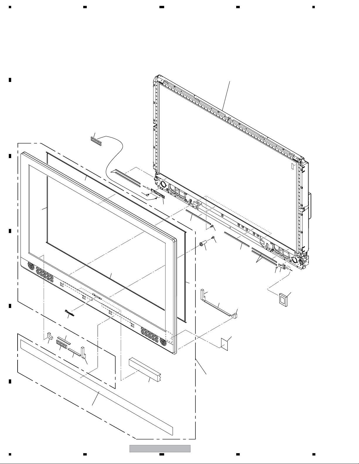
2.5 CHASSIS SECTION (2/2)
A
H
9
G
22
F
5
19
8
12
26
28
26
14
26
26
E
8
26
A
10
8
MAIN
CN4001
11
B
28
26
8
B
C
13
42E AUDIO
D
CN3751
I
J
F
MAIN
CN4008
37
I
17
C
20
36
36
J
K
L
36
4
23
K
37
33
M
28
H
32
N
21
D
34
28
34
27
28
34
28
34
30
25
Q
28
28
29
31
L
16
35
35
M
27
G
24
6
28
25
MAIN
CN4002
28
15
37
7
AC inlet,
Power switch
28
O
P
28
18
R
36
E
36
3
35
34
37
O
36
E
N
A
25
1
28
B
K
C
25
Q
R
F
Q
D
36
R
P
35
29
Refer to
18
"2.6 PANEL CHASSIS SECTION".
PDP-427XD
2
1234

5678
CHASSIS SECTION (2/2) PARTS LIST
No. Description Part No.
Mark
1 SUS CLAMP 1 Assy AWW1022
2 SUS CLAMP 2 Assy AWW1023
3 42 X DRIVE Assy AWW1196
4 42 Y DRIVE Assy AWV2400
5 42 DIGITAL Assy AWW1240
6 SENSOR Assy AWW1140
7POWER SUPPLY Unit AXY1153
8Ferrite Core ATX1048
9 Flexible Cable (J201) ADD1429
10 Flexible Cable (J202) ADD1430
>
A
11 Flexible Cable (J203) ADD1431
12 Flexible Cable (J204) ADD1432
13 Flexible Cable (J205) ADD1433
14 Flexible Cable (J206) ADD1434
15 6P Housing Wire (J118) ADX3118
16 3P Housing Wire (J119) ADX3122
17 9P Housing Wire (J101) ADX3318
18 8P&5/4P Housing Wire (J102) ADX3319
19 14P Housing Wire (J105) ADX3323
20 6P/4P Housing Wire (J108) ADX3326
21 4P Housing Wire (J109) ADX3327
22 5P Housing Wire (J110) ADX3328
23 Spacer AEC1065
24 Nyron Rivet AEC1671
25 Wire Saddle AEC1745
26 Flat Clamp AEC1879
27 PCB Support AEC1938
28 Re-use PCB Spacer AEC2087
29 Drive Silicone Sheet AEH1095
30 Power Supply Sheet B (507) AMR3555
B
C
D
31 Y Drive Protection Sheet A AMR3632
32 Y Drive Protection Sheet B AMR3633
33 Power Supply Sheet (427) A AMR3648
34 Rivet A BEC1158
35 Screw ABA1364
36 Screw ABA1351
37 Screw ABA1368
56
PDP-427XD
E
F
19
7
8
1234
2.6 PANEL CHASSIS SECTION
A
5
B
4
8
8
8
8
8
7
8
C
10
13
6
D
E
3
2
11
14
9
1
12
F
20
1234
PDP-427XD
5678
(1) PANEL CHASSIS SECTION PARTS LIST
No. Description Part No.
Mark
NSP 1 Panel Chassis (427S) Assy See Contrast table (2)
NSP 2 Plasma Panel (42DC) Assy AWU1161
NSP 3 42 ADDRESS Assy AWV2335
NSP 4 42 SCAN A Assy AWW1182
NSP 5 42 SCAN B Assy AWW1183
6 Address Heatsink ANH1644
7 Conductive Plate X ANG2791
8 Re-use PCB Spacer AEC2087
9 Address Silicone A AEH1093
10 Conductive Plate Holder AMR3446
A
11 Address Holder Assy AMR3460
12 Screw ABA1364
13 Screw BBB30P120FNI
14 Tube Cover (FT) AMR3557
(2) CONTRAST TABLE
PDP-427XD/WYVIXK5, PDP-4270XD/WYVIXK5, PDP-4270XA/WYVIXK5, WYV5, PDP-427XA/WYVIXK5 and
WYV5 are constructed the same except for the following:
Mark No. Symbol and Description
NSP 1 Panel Chassis (427S) Assy AWU1185 AWU1185 AWU1185 AWU1185 AWU1207 AWU1207
PDP-427XD
/WYVIXK5
PDP-4270XD
/WYVIXK5
PDP-4270XA
/WYVIXK5
PDP-427XA
/WYVIXK5
PDP-4270XA
/WYV5
PDP-427XA
/WYV5
B
C
D
56
PDP-427XD
E
F
21
7
8
1234
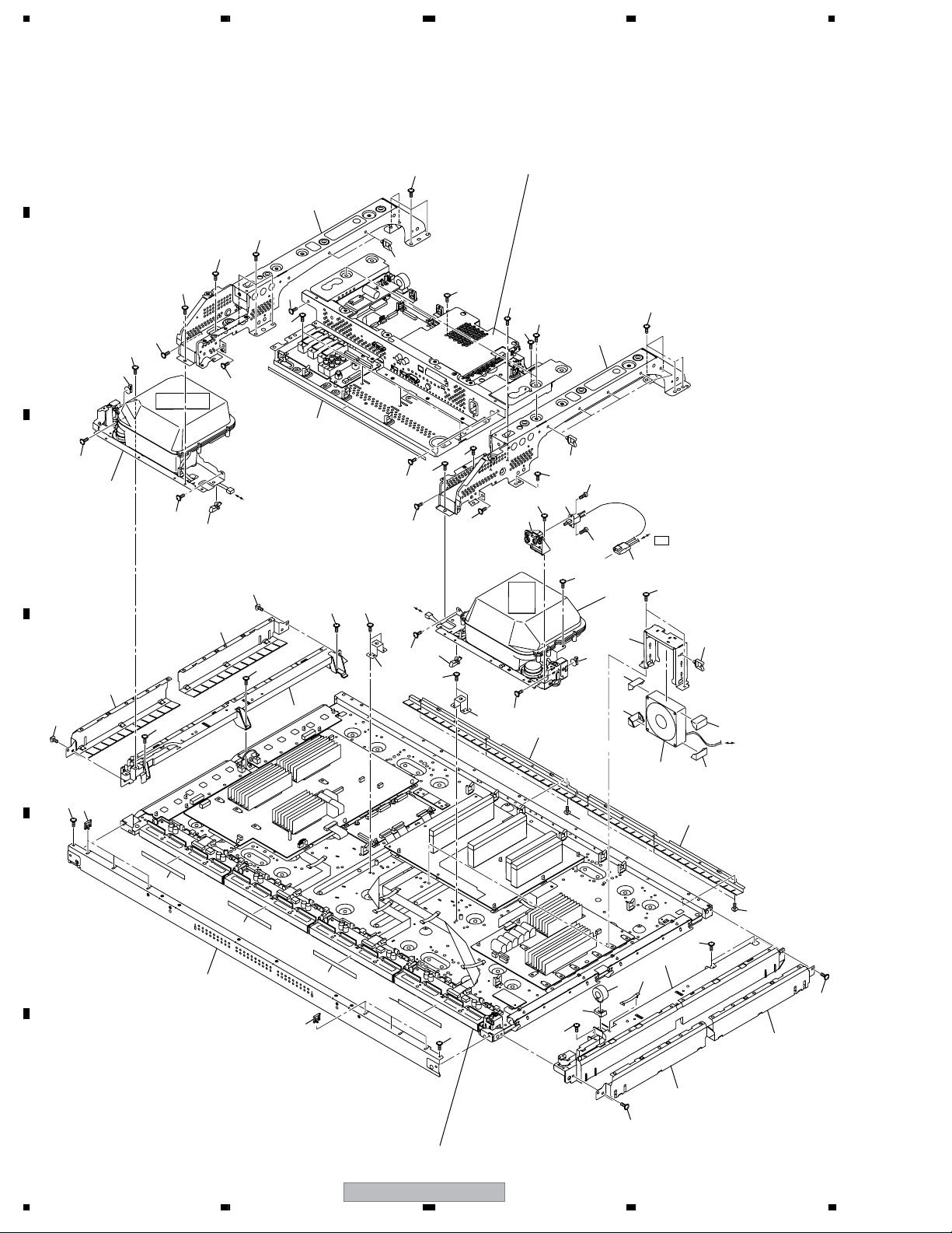
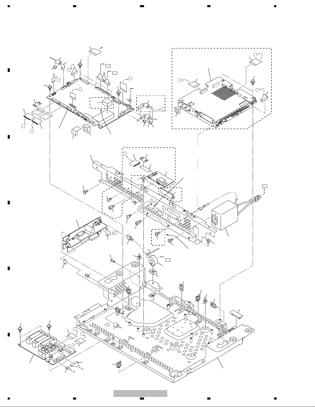
2.7 MULTI BASE SECTION
A
39
41
42 DIGITAL
CN3001
POWER
P8
POWER
17
P9
47
PDP-4270XD,
PDP-427XD only
29
5
H
Fan
PDP-4270XD,
15
F
PDP-427XD only
42
G
20
24
24
42
31
7
D
38
PDP-427XD,
PDP-427XA only
13
24
42
D
21
47
A
SIDE KEY CN9501
LED IR CN9701
47
F
31
B
8
B
C
8
1
40
36
PDP-4270XD,
PDP-427XD only
H
9
47
16
G
14
C
3
PDP-427XD,
47
43
46
PDP-427XA only
PDP-4270XD,
34
PDP-427XD only
POWER
P3
4
44
46
18
25
44
24
45
POWER
P5
43
PDP-4270XD,
PDP-427XD only
10
43
D
A
19
33
6
23
33
30
27
26
30
25
26
E
28
47
47
12
B
C
42
30
Speaker
11
F
2
32
SIDE
CN9205
SIDE
CN9207
22
30
35
22
PDP-427XD
1234
5678
(1) MULTI BASE SECTION PARTS LIST
No. Description Part No.
Mark
1 MAIN Assy See Contrast table (2)
2TANSHI Assy See Contrast table (2)
3 PC Assy See Contrast table (2)
4 42E AUDIO Assy AWW1185
5 R07 DT Assy See Contrast table (2)
>
>
>
>
>
No. Description Part No.
Mark
26 Wire Saddle AEC1745
27 Ferrite Core Holder AEC1818
28 Clamp AEC1884
29 3P Housing Wire (J127) ADX3421
30 Re-use Wire Saddle AEC1945
A
6Ferrite Core ATX1044
7Ferrite Core See Contrast table (2)
8Ferrite Core ATX1064
9 Flexible Cable (J214) See Contrast table (2)
10 AC Inlet (CN1) AKP1301
11 Flexible Cable (J210) ADD1441
12 Flexible Cable (J211) ADD1441
13 Flexible Cable (J207) ADD1445
14 Flexible Cable (J213) See Contrast table (2)
15 Flexible Cable (J215) See Contrast table (2)
16 12P Housing Wire (J126) See Contrast table (2)
17 13P&11P Housing Wire (J106) ADX3324
18 3P Housing Wire (J107) ADX3325
19 11P Housing Wire (J111) ADX3329
20 6P Housing Wire (J113) ADX3331
21 7/6/4P Housing Wire (J114) ADX3332
22 14P Housing Wire (J116) ADX3334
23 8/4P Housing Wire (J117) ADX3336
24 Binder AEC-093
25 Locking Card Spacer AEC1429
31 Ferrite Stopper AEC1981
32 5P Housing Wire (J125) ADX3388
33 Locking Card Spacer AEC2019
34 POD Cover See Contrast table (2)
35 Multi Base Assy See Contrast table (2)
36 Terminal Panel A See Contrast table (2)
37 • • • • •
38 Gasket N See Contrast table (2)
39 Gasket EA ANK1855
40 Gasket EB ANK1899
41 Gasket ED See Contrast table (2)
42 Filter CTX1054
43 Screw AMZ30P060FTB
44 Hex. Head Screw BBA1051
45 Screw See Contrast table (2)
46 Screw BMZ30P060FTB
47 Screw PMB30P080FNI
B
C
(2) CONTRAST TABLE
PDP-427XD/WYVIXK5, PDP-4270XD/WYVIXK5, PDP-4270XA/WYVIXK5, WYV5, PDP-427XA/WYVIXK5 and
WYV5 are constructed the same except for the following:
Mark No. Symbol and Description
1 MAIN Assy AWV2318 AWV2320 AWV2320 AWV2318 AWV2320 AWV2318
2TANSHI Assy AWW1161 AWW1178 AWW1178 AWW1161 AWW1178 AWW1161
3 PC Assy AWW1163 Not used Not used AWW1163 Not used AWW1163
5 R07 DT Assy AWE1311 AWE1311 Not used Not used Not used Not used
7Ferrite Core ATX1063 Not used Not used ATX1063 Not used ATX1063
9 Flexible Cable (J214) ADD1450 ADD1450 Not used Not used Not used Not used
14 Flexible Cable (J213) ADD1452 Not used Not used ADD1452 Not used ADD1444
15 Flexible Cable (J215) ADD1451 ADD1451 Not used Not used Not used Not used
16 12P Housing Wire (J126) ADX3390 ADX3390 Not used Not used Not used Not used
34 POD Cover AMR3542 AMR3542 Not used Not used Not used Not used
35 Multi Base Assy ANA1952 ANA1952 ANA2019 ANA2019 ANA2019 ANA2019
36 Terminal Panel A ANC2398 ANC2400 ANC2415 ANC2399 ANC2415 ANC2399
>
38 Gasket N ANK1776 ANK1776 Not used Not used Not used Not used
>
41 Gasket ED ANK1863 ANK1863 Not used Not used Not used Not used
45 Screw
PDP-427XD
/WYVIXK5
BBZ30P060FTB BBZ30P060FTB
PDP-4270XD
/WYVIXK5
PDP-4270XA
/WYVIXK5
Not used Not used Not used Not used
PDP-427XA
/WYVIXK5
PDP-4270XA
/WYV5
PDP-427XA
/WYV5
D
E
F
56
PDP-427XD
23
7
8
1234
2.8 PDP SERVICE PANEL ASSY 427 (AWU1208)
4
A
4
23
4
23
23
4
23
22
1
21
B
23
4
23
4
C
D
22
1
21
PDP SERVICE PANEL ASSY 427 (AWU1208) PARTS LIST
Mark No. Description Part No.
NSP 1 Panel Chassis (427) Assy AWU1171
2 Caution Label AAX3031
NSP 3 Drive Voltage Label ARW1097
4 Screw PMB50P150FTC
5 Screw ABA1351
20
Mark No. Description Part No.
16 Pad 42SINGLE(B-L) AHA2552
17 Pad 42SINGLE(B-R) AHA2553
18 Upper Carton (42SINGLE) AHD3480
19 Under Carton (42SINGLE) AHD3481
20 Polyethylene Bag AHG1381
6 Wire Saddle AEC1745
E
7 PCB Support AEC1938
8 Vinyl Bag S AHG1338
NSP 9 Vinyl Bag AHG1340
10 Y Drive Protection Sheet A AMR3632
11 Power Sheet (427) A AMR3648
12 Address Gasket (42) ANK1877
13 Rivet A BEC1158
14 Pad 42SINGLE(T-L) AHA2550
15 Pad 42SINGLE(T-R) AHA2551
F
24
1234
21 Packing Sheet AHG1386
22 Tray (FT) AHX1158
23 Cup Spacer (15) ANG2936
PDP-427XD
5678
2.9 TABLE TOP STAND (PDP-4270XD and PDP-4270XA ONLY)
5
5
2
4
3
1
3
4
1
A
B
C
TABLE TOP STAND PARTS LIST
Mark No. Description Part No.
1 Stand Pipe Assy See Contrast table (2)
2 Base Cover Assy See Contrast table (2)
3 Screw ABA1357
4 Screw (HEX) SMZ80H300FTC
5 Screw (HEX) ABA1365
(2) CONTRAST TABLE
PDP-4270XD/WYVIXK5, PDP-4270XA/WYVIXK5 and PDP-4270XA/WYV5 are constructed the same except for
the following:
Mark No. Symbol and Description
1 Stand Pipe Assy AXY1158 AXY1158 AXY1144
2 Base Cover Assy AXY1161 AXY1161 AXY1143
PDP-4270XD
/WYVIXK5
PDP-4270XA
/WYVIXK5
PDP-4270XA
/WYV5
D
E
F
56
PDP-427XD
25
7
8
1234
3. PCB PARTS LIST
>
NOTES:
A
Parts marked by "NSP" are generally unavailable because they are not in our Master Spare Parts List.
The mark found on some component parts indicates the importance of the safety factor of the part.
Therefore, when replacing, be sure to use parts of identical designation.
When ordering resistors, first convert resistance values into code form as shown in the following examples.
Ex.1 When there are 2 effective digits (any digit apart from 0), such as 560 ohm and 47k ohm (tolerance is shown by J=5%,
and K=10%).
560 Ω
47k Ω
0.5 Ω
1 Ω
56 x 10
47 x 10
R50
1R0
1
3
561
473
RD1/4PU J
RD1/4PU J
RN2H K
RS1P K
561
473
R50
1R0
Ex.2 When there are 3 effective digits (such as in high precision metal film resistors).
5.62k Ω
7777 LIST OF WHOLE PCB ASSEMBLIES
B
Mark Symbol and Description
1..R07 DT ASSY AWE1311 AWE1311 Not used Not used Not used Not used
1..MAIN ASSY AWV2318 AWV2320 AWV2320 AWV2318 AWV2320 AWV2318
NSP 1..IO ASSY AWV2319 AWV2321 AWV2321 AWV2319 AWV2321 AWV2319
2..TANSHI ASSY AWW1178 AWW1161 AWW1161 AWW1178 AWW1161 AWW1161
2..SIDE ASSY AWW1162 AWW1162 AWW1162 AWW1162 AWW1162 AWW1162
2..PC ASSY AWW1163 Not used Not used AWW1163 Not used AWW1163
NSP 1..42E AUDIO ASSY AWV2369 AWV2369 AWV2369 AWV2369 AWV2369 AWV2369
C
2..SIDE KEY ASSY AWW1133 AWW1133 AWW1133 AWW1133 AWW1133 AWW1133
2..42 & 60 LED ASSY AWW1134 AWW1134 AWW1134 AWW1134 AWW1134 AWW1134
2..LED IR ASSY AWW1136 AWW1136 AWW1136 AWW1136 AWW1136 AWW1136
2..42E AUDIO ASSY AWW1185 AWW1185 AWW1185 AWW1185 AWW1185 AWW1185
1
5621
PDP-427XD
/WYVIXK5
PDP-4270XD
/WYVIXK5
PDP-4270XA
/WYVIXK5
RN1/4PC F562 x 10
PDP-427XA
/WYVIXK5
5621
PDP-4270XA
/WYV5
PDP-427XA
/WYV5
NSP 1..42 X DRIVE ASSY AWV2399 AWV2399 AWV2399 AWV2399 AWV2399 AWV2399
2..SUS CLAMP 1 ASSY AWW1022 AWW1022 AWW1022 AWW1022 AWW1022 AWW1022
2..SUS CLAMP 2 ASSY AWW1023 AWW1023 AWW1023 AWW1023 AWW1023 AWW1023
2..42 X DRIVE ASSY AWW1196 AWW1196 AWW1196 AWW1196 AWW1196 AWW1196
1..42 Y DRIVE ASSY AWV2400 AWV2400 AWV2400 AWV2400 AWV2400 AWV2400
NSP 1..42 DIGITAL ASSY AWV2435 AWV2435 AWV2435 AWV2435 AWV2435 AWV2435
D
E
2..SENSOR ASSY AWW1140 AWW1140 AWW1140 AWW1140 AWW1140 AWW1140
2..42 DIGITAL ASSY AWW1240 AWW1240 AWW1240 AWW1240 AWW1240 AWW1240
NSP 1..PANEL CHASSIS (427S) ASSY AWU1185 AWU1185 AWU1185 AWU1185 AWU1185 AWU1185
NSP 2..42 ADDRESS ASSY AWV2335 AWV2335 AWV2335 AWV2335 AWV2335 AWV2335
NSP 2..42 SCAN ASSY AWV2362 AWV2362 AWV2362 AWV2362 AWV2362 AWV2362
NSP 3..42 SCAN A ASSY AWW1182 AWW1182 AWW1182 AWW1182 AWW1182 AWW1182
NSP 3..42 SCAN B ASSY AWW1183 AWW1183 AWW1183 AWW1183 AWW1183 AWW1183
1..POWER SUPPLY UNIT AXY1153 AXY1153 AXY1153 AXY1153 AXY1153 AXY1153
F
26
1234
PDP-427XD
5678
7777 CONTRAST OF PCB ASSEMBLIES
MAIN ASSY
AWV2320 and AWV2318 are constructed the same except for the following :
Mark Symbol and Description AWV2320 AWV2318
IC5103 Not used TVP5150AM1PBS-K
IC5404 Not used BR24L02FJ
IC8305 Not used TC74VHC00FTS1
Q5402 Not used HN1K02FU
Q5408 Not used UMD2N
Q5414 Not used RN1902
Q8302 Not used 2SA1586
Q8303, Q8304 Not used DTC124EUA
Q8311 Not used 2SJ461A
D5402 Not used 1SS301
D5408 Not used UDZS6R8(B)
D8301 - D8303 Not used 1SS355
C4922, C4932, C4933, C5101, C5102, C5103 Not used CKSRYB105K10
C5104, C5105 Not used CCSSCH100D50
C5117, C5123, C5125, C5126, C5449 - C5451 Not used CKSSYF104Z16
C5121, C5122, C5124, C8320 Not used CKSSYB104K10
C5452, C8319 Not used DCH1201
C5453 Not used CCSSCH101J50
R4031 Not used RS1/16S0R0J
R4056, R8344 Not used RS1/16SS0R0J
R4057 RS1/16SS0R0J Not used
R4728, R4729, R4904, R4905, R4910 Not used RS1/16SS220J
R4809, R4810 Not used RS1/16SS562J
R4964, R4965, R4966 Not used RS1/16S75R0F
R5103 Not used ACN1246
A
B
C
R5121, R8347, R8359 Not used RS1/16SS332J
R5122, R5419, R8476 Not used RS1/16SS103J
R5124, R5125, R5126 Not used RS1/16SS470J
R5147 Not used RAB4CQ220J
R5421, R8364 Not used RS1/16SS101J
R5422 Not used RS1/16SS473J
R5423, R5424 Not used RS1/16SS100J
R5433, R8353 Not used RS1/16SS102J
R8354 Not used RS1/16SS122J
R8355 Not used RS1/16SS104J
R8356, R8358 Not used RS1/16S122J
R8357 Not used RS1/16S220J
R8376 RS1/10S0R0J Not used
R8379, R8380 RS1/16SS223J Not used
R8477, R8480 RS1/16SS103J Not used
X5101 CRYSTAL Not used ASS1189
CN4018 12P FFC CONNECTOR Not used AKM1233
JA5402 HDMI CONNECTOR Not used AKP1278
D
E
56
PDP-427XD
F
27
7
8
1234
TANSHI ASSY
AWW1178 and AWW1161 are constructed the same except for the following :
Mark Symbol and Description AWW1178 AWW1161
A
B
77
77
Mark No. Description Part No.
C
Q9012 Not used HN1A01FU
Q9015 Not used 2SC4116
Q9016 Not used 2SD2114K
F9001 - F9007 Not used CTF1557
C9037 Not used CCG1205
C9022, C9025 Not used CKSRYB105K10
C9010 - C9012 Not used CKSSYB471K50
C9023, C9026 Not used CKSRYB102K50
C9043 Not used CKSRYB224K10
JA9005 2P PINJACK AKB1331 AKB1340
JA9002 Not used VKN1449
JA9004 Not used AKN1081
PCB PARTS LIST FOR PDP-427XD/WYVIXK5 UNLESS OTHER WISE NOTED
Mark No. Description Part No.
R07 DT ASSY
MISCELLANEOUS
9 TOP CAN XNG1002
11 PCMCIA EJECTOR ANG2673
12-15 SCREW PMZ20P100FNI
16-18 SCREW ABZ30P060FTC
[TUNER BLOCK]
C1018,1027,1029,1050 CEHVKW470M16
C1019 CEHVKW100M50
C1020 CEHVKW100M16
C1025,1026,1030-1035 CKSRYB104K16
C1028,1038,1042,1046 CCG1205
C1036 CKSRYB105K10
C1037,1039,1049,1053 CKSRYB104K16
C1043,1044 CCSRCJ3R0C50
C1045 CKSRYB103K50
C1051 CCG1205
>
>
SEMICONDUCTORS
IC1000 UPC3221GV
IC1001 STV0361L
Q1001 2SC2412K
Q1002 DTC124EUA
Q1003,1004 RK7002
D
>
D1000 SM15T6V8A
D1001 1SS355
MISCELLANEOUS
L1000 XTX1005
L1002 LCYAR82J2520
L1004 XTX1003
L1200 XTX1001
F1000 XTF1002
F1001,1003-1010 VTF1091
E
F1012-1014,1100,1101 VTF1091
F1202-1204 VTF1091
X1100 CRYSTAL (27 MHz) XSS1010
>
FU1200 CHIP FUSE (0.25A) XEK1003
>
M1000 FRONT END XXF1007
CAPACITORS
C1001-1003,1017,1022 CKSRYB104K16
C1004,1055 CEHVKW101M6R3
C1010 CEHVKW2R2M50
C1013,1021,1040,1041 CKSRYB103K50
C1015 CKSRYB102K50
F
C1054 BCG1050
C1056,1057 CEHVKW470M16
C1058-1062 CKSRYB104K16
C1102 CEHVKW331M6R3
RESISTORS
All Resistors RS1/16S###J
[DEMUX BLOCK]
SEMICONDUCTORS
IC2000 STI5517DWAL
IC2001 SN74LVU04APW
IC2002 TC74VHC08FTS1
Q2000 2SC4081
D2000 DA204U
D2001 UDZS8R2(B)
D2002 HVU307
D2005,2009 RB501V-40
MISCELLANEOUS
L2000 XTX1003
F2000-2003 VTF1091
X2000
CRYSTAL RESONATOR (27 MHz)
X2001 CRYSTAL OSCILLATOR ASS1172
VA2002 VARISTOR
BSS1112
AVR-M1608C120MT2AB
RESISTORS
R2010,2018,2042 RAB4C103J
R2070,2071 RAB4CQ220J
Other Resistors RS1/16S###J
28
PDP-427XD
1234

5678
Mark No. Description Part No.
Mark No. Description Part No.
CAPACITORS
C2000,2026,2030 CCSRCH101J50
C2001 CKSRYB471K50
C2002,2003,2005,2006 CKSRYF104Z16
C2004 CKSRYF474Z16
C2007 CCSRCH471J50
C2008,2017,2020,2021 CKSRYB102K50
C2009 CCSRCH330J50
C2011,2012 CCSRCH390J50
C2013 CKSRYB105K10
C2014,2016 CCSRCH100D50
C2015 CKSRYF105Z10
C2018,2019,2022-2025 CKSRYF104Z16
C2027,2029,2042,2046 CKSRYF223Z50
C2028,2035,2037-2041 CKSRYF104Z16
C2032-2034,2036 CEHVKW470M16
C2043-2045,2047,2048 CKSRYF104Z16
[MEMORY BLOCK]
SEMICONDUCTORS
IC3000,3003 K4S281632I-UC75
IC3002 XGC1003
MISCELLANEOUS
L3003 XTX1003
L3005 XTX1001
RESISTORS
R3004-3014 RAB4CQ470J
Other Resistors RS1/16S###J
CAPACITORS
C3000,3003,3007,3008 CKSRYF104Z16
C3001,3002,3004,3014 CKSRYF223Z50
C3010 CEHVKW470M16
C3012,3017,3020-3022 CKSRYF104Z16
C3015,3018,3019,3023 CKSRYF223Z50
CAPACITORS
C4000,4002 CCG1205
C4001,4014,4032,4033 CKSRYB103K50
C4003,4005,4017,4018 CKSRYF104Z16
C4004 CEHVKW2R2M50
C4006 CKSRYB102K50
C4007,4013 CCSRCH220J50
C4008,4009 CCSRCH121J50
C4010,4011,4042 CCSRCH101J50
C4012,4022,4023,4029 CEHVKW470M16
C4019,4102-4104 CEHVKW100M16
C4021,4024,4043 CKSRYF104Z16
C4038 CKSRYB103K50
C4039 CEHVKW470M16
C4040,4041 CKSRYB105K10
C4105-4107 CKSRYF104Z16
C4108-4113 CEHVKW100M16
[CI BLOCK]
SEMICONDUCTORS
IC5000 ST890CDR
IC5001 CIMAXSP2L
IC5002 TC74LCX245FTS1
IC5003,5004 TC74LCX373FT
Q5000 2SC4081
Q5001 DTA143EUA
Q5002 DTC124EUA
MISCELLANEOUS
CN5000 PCMCIA CONNECTOR XKP1003
RESISTORS
R5014,5019,5022,5024 RAB4CQ470J
R5030,5032,5036-5038 RAB4CQ470J
R5045-5050 RAB4CQ470J
Other Resistors RS1/16S###J
A
B
C
D
C3024 CKSRYF223Z50
[AV BLOCK]
SEMICONDUCTORS
IC4000 CS4334-KS
IC4001 SN74LVU04APW
IC4002 RC4558D
IC4003 CS8406CZZ
IC4100 PCM1803DB
Q4001,4002 2SC4081
MISCELLANEOUS
F4000,4100 FERRITE CORE VTF1091
JA4000 OPTICAL OUT MOD. GP1FM513TZ
X4000 CRYSTAL (12.288 MHz) XSS1006
CN4000 40P CONNECTOR AKM1348
RESISTORS
R4042,4045,4046 RS1/16S2000F
Other Resistors RS1/16S###J
56
CAPACITORS
[POWER BLOCK]
SEMICONDUCTORS
PDP-427XD
C5001 CKSRYB105K10
C5003,5004,5006 CKSRYF104Z16
C5005,5100 CEHVKW470M16
C5008-5013 CKSRYF104Z16
IC6001 M5291FP
IC6002 BA05FP
IC6003 FPF2003
IC6200 TC74LCX245FTS1
IC6300 SN74LVC1G08DCK
Q6001,6009,6011,6200 DTC124EUA
Q6003,6005,6010 DTA143EUA
Q6006 2SB1188
Q6008 TPC8209
Q6100 2SC4081
D6001 RSX201L-30
D6003,6100-6102 1SS355
D6103 UDZS30(B)
7
8
E
F
29

1234
Mark No. Description Part No.
MISCELLANEOUS
L6000 LCYAR82J2520
A
L6001,6100,6101 XTH1001
F6000 FERRITE CORE VTF1091
CN6000 12P CONNECTOR AKM1298
CN6003 50P CONNECTOR AKM1349
RESISTORS
R6012-6014 RAB4C2R2J
R6031 RAB4C221J
R6204,6205 RAB4CQ101J
Other Resistors RS1/16S###J
CAPACITORS
C6000,6026,6104-6106 CEHVKW331M6R3
B
C6001,6011,6013-6015 CEHVKW470M16
C6002,6035 CKSRYF223Z50
C6003,6005,6006,6012 CKSRYF104Z16
C6004 CEHVKW100M50
C6008,6016 CKSRYF474Z16
C6010 CCSRCH331J50
C6017,6028,6036,6042 CEHVKW101M6R3
C6018,6020,6021,6025 CKSRYF104Z16
C6019,6023,6100 CEHVKW470M16
C6022 CKSRYB103K50
C6027 CCSRCH101J50
C
C6029,6030,6033,6038 CKSRYF104Z16
C6031 CEHVKW2R2M50
C6044 CEHVKW101M6R3
Mark No. Description Part No.
C4048-4050 CCSSCH470J50
[REG 0 BLOCK]
SEMICONDUCTORS
IC4101,4114,4115 S-1132B18-U5
IC4102 LTC3414EFE
IC4103 LTC3412EFE
IC4104,4111,4113 NJM2846DL3-05
IC4105 S-1170B25UC-OTK
IC4106 S-1170B15UC-OTA
IC4107 NJM2846DL3-33
IC4108 NJM2846DL3-18
IC4109,4110 PQ090DNA1ZPH
Q4101,4103 RN1902
Q4102 HN1C01FU
Q4104 DTC124EUA
Q4105,4106 UPA1917TE
Q4107-4109 2SC4116
Q4110 2SD2114K
D4101-4110,4112-4118 1SS355
D4111,4119,4120,4122 1SS357
D4121 1SS355
MISCELLANEOUS
L4101,4103 BTX1042
L4102,4105-4107 BTX1039
L4108 ATH1208
L4109 ATH1194
F4101,4102 VTF1080
C6102 CCG1191
C6200,6300 CKSRYF104Z16
MAIN ASSY
[BOARD IF BLOCK]
D
SEMICONDUCTORS
IC4001-4005 TC74VCX541FT
Q4001,4002,4005 DTC124EUA
Q4003,4004 RN2902
MISCELLANEOUS
L4001-4006 BTX1042
>
F4001-4010 CTF1557
CN4001,4004,4005 50P CONNECTOR AKM1349
CN4006 PLUG(6P) KM200NA6
CN4013 50P CONNECTOR PBF AKM1353
E
CN4014 40P CONNECTOR PBF AKM1354
RESISTORS
R4001 RAB4CQ470J
R4021-4024 BCN1067
R4030,4035 RS1/16S0R0J
Other Resistors RS1/16SS###J
RESISTORS
R4113,4134-4136,4140 RS1/10S0R0J
R4119,4131,4146 RS1/16SS3003F
R4120 RS1/16SS2003F
R4123,4159 RS1/16SS1502F
R4124 RS1/16SS6202F
R4133 RS1/16SS1503F
R4148,4164-4170,4173 RS1/10S0R0J
Other Resistors RS1/16SS###J
CAPACITORS
C4018,4101,4103,4106 CKSRYB105K10
C4102,4104,4105,4107 DCH1201
C4108 CKSRYB105K10
C4109,4111-4113,4116 DCH1201
C4110,4117 CCSSCH101J50
C4114,4118 BCG1050
C4119,4127,4131,4134 DCH1201
C4121,4140,4153 CKSSYB104K10
C4122,4129 CCSSCH220J50
C4123,4124,4126,4130 DCH1165
C4132 ACH1421
C4135,4138,4143-4146 DCH1201
C4136,4137,4141,4142 BCG1059
C4139 CCSRCH471J50
C4147 CCSRCH102J50
CAPACITORS
C4001-4003,4007,4009 CKSSYF104Z16
C4004 CCSSCH101J50
C4006,4036,4039 DCH1201
F
C4008 DCH1165
C4014 CKSSYF104Z16
C4033,4051 CKSRYF104Z50
30
1234
C4150 ACH1429
C4151 CKSSYB102K50
C4154 CKSSYF104Z16
C4155 CKSSYB103K16
C4165 DCH1201
PDP-427XD
 Loading...