

Page 1
PIONEER CORPORATION 4-1, Meguro 1-chome, Meguro-ku, Tokyo 153-8654, Japan
PIONEER ELECTRONICS (USA) INC. P.O. Box 1760, Long Beach, CA 90801-1760, U.S.A.
PIONEER EUROPE NV Haven 1087, Keetberglaan 1, 9120 Melsele, Belgium
PIONEER ELECTRONICS ASIACENTRE PTE. LTD. 253 Alexandra Road, #04-01, Singapore 159936
PIONEER CORPORATION 2006
ORDER NO.
PROVISIONAL
PDP-4270XD
PLASMA TELEVISION
PDP-4270XD
PDP-427XD
PDP-4270XA
PDP-427XA
THIS MANUAL IS APPLICABLE TO THE FOLLOWING MODEL(S) AND TYPE(S).
Model Type Power Requirement Remarks
PDP-4270XD WYVIXK5 AC 220 V to 240 V
PDP-427XD WYVIXK5 AC 220 V to 240 V
PDP-4270XA
PDP-427XA
This service manual should be used together with the following manual(s).
PDP-4270XD, PDP-427XD,
PDP-4270XA, PDP-427XA
WYVIXK5 AC 220 V to 240 V
WYV5 AC 220 V to 240 V
WYVIXK5 AC 220 V to 240 V
WYV5 AC 220 V to 240 V
Model No. Order No. Remarks
ARP3392 SCHEMATIC DIAGRAM, PCB CONNECTION DIAGRAM
For details, refer to "Important Check Points for good servicing".
T-IZR SEP. 2006 printed in Japan
Page 2

1234
1. NOTES ON SERVICE VISIT
1.1 SAFETY INFORMATION
A
This service manual is intended for qualified service technicians ; it is not meant for the casual
do-it-yourselfer. Qualified technicians have the necessary test equipment and tools, and have been
trained to properly and safely repair complex products such as those covered by this manual.
Improperly performed repairs can adversely affect the safety and reliability of the product and may
void the warranty. If you are not qualified to perform the repair of this product properly and safely,
you should not risk trying to do so and refer the repair to a qualified service technician.
WARNING
This product contains lead in solder and certain electrical parts contain chemicals which are known to the state of California to
B
cause cancer, birth defects or other reproductive harm.
NOTICE
(FOR CANADIAN MODEL ONLY)
Fuse symbols (fast operating fuse) and/or (slow operating fuse) on PCB indicate that replacement parts
must be of identical designation.
Health & Safety Code Section 25249.6 - Proposition 65
REMARQUE
(POUR MODÈLE CANADIEN SEULEMENT)
Les symboles de fusible (fusible de type rapide) et/ou (fusible de type lent) sur CCI indiquent que les pièces
C
de remplacement doivent avoir la même désignation.
SAFETY PRECAUTIONS
NOTICE : Comply with all cautions and safety related notes
located on or inside the cabinet and on the chassis.
The following precautions should be observed :
1. When service is required, even though the PDP UNIT an
isolation transformer should be inserted between the power line
D
and the set in safety before any service is performed.
2. When replacing a chassis in the set, all the protective devices
must be put back in place, such as barriers, nonmetallic knobs,
adjustment and compartment covershields, isolation resistorcapacitor, etc.
3. When service is required, observe the original lead dress. Extra
precaution should be taken to assure correct lead dress in the
high voltage circuitry area.
4. Always use the manufacture's replacement components.
Especially critical components as indicated on the circuit
diagram should not be replaced by other manufacture's.
Furthermore where a short circuit has occurred, replace those
E
components that indicate evidence of overheating.
5. Before returning a serviced set to the customer, the service
technician must thoroughly test the unit to be certain that it is
completely safe to operate without danger of electrical shock,
and be sure that no protective device built into the set by the
manufacture has become defective, or inadvertently defeated
during servicing. Therefore, the following checks should be
performed for the continued protection of the customer and
servicetechnician.
6. Perform the following precautions against unwanted radiation
and rise in internal temperature.
• Always return the internal wiring to the original styling.
• Attach parts (Gascket, Ferrite Core, Ground, Rear Cover,
Shield Case etc.) surely after disassembly.
7. Perform the following precautions for the PDP panel.
• When the front case is removed, make sure nothing hits the
panel face, panel corner, and panel edge (so that the glass does
not break).
• Make sure that the panel vent does not break. (Check that the
cover is attached.)
• Handle the FPC connected to the panel carefully.
Twisting or pulling the FPC when connecting it to the
connector will cause it to peel off from the panel.
8. Pay attention to the following.
• Pay extreme caution when the front case and rear panel are
removed because this may cause a high risk of disturbance to
TVs and radios in the surrounding.
F
2
1234
PDP-4270XD
Page 3
5678
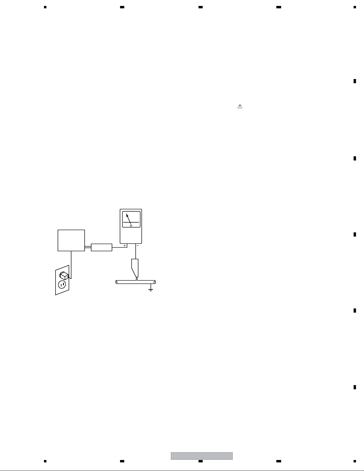
Leakage Current Cold Check
With the AC plug removed from an AC power source, place a
jumper across the two plug prongs. Turn the AC power switch on.
Using an insulation tester (DC 500V), connect one lead to the
jumpered AC plug and touch the other lead to each exposed metal
part (input/output terminals, screwheads, metal overlays, control
shafts, etc.), particularly any exposed metal part having a return
path to the chassis. Exposed metal parts having a return path to
the chassis should have a minimum resistor reading of 0.3MΩ
and a maximum resistor reading of 5MΩ. Any resistor value
below or above this range indicates an abnormality which requires
corrective action. Exposed metal parts not having a return path to
the chassis will indicate an open circuit.
Leakage Current Hot Check
Plug the AC line cord directly into an AC power source (do not
use an isolation transformer for this check).
Turn the AC power switch on.
Using a "Leakage Current Tester (Simpson Model 229
equivalent)", measure for current from all exposed metal parts of
the cabinet (input/output terminals, screwheads, metal overlays,
control shaft, etc.), particularly any exposed metal part having a
return path to the chassis, to a known earth ground (water pipe,
conduit, etc.). Any current measured must not exceed 0.5mA.
PRODUCT SAFETY NOTICE
Many electrical and mechanical parts in PIONEER set have
special safety related characteristics. These are often not evident
from visual inspection nor the protection afforded by them
necessarily can be obtained by using replacement components
rated for higher voltage, wattage, etc. Replacement parts which
have these special safety characteristics are identified in this
Service Manual.
Electrical components having such features are identified by
marking with a on the schematics and on the parts list in this
Service Manual.
The use of a substitute replacement component which dose not
have the same safety characteristics as the PIONEER
recommended replacement one, shown in the parts list in this
Service Manual, may create shock, fire or other hazards.
Product Safety is continuously under review and new instructions
are issued from time to time. For the latest information, always
consult the current PIONEER Service Manual. A subscription to,
or additional copies of, PIONEER Service Manual may be
obtained at a nominal charge from PIONEER.
A
B
C
Reading should
not be above
0.5mA
Earth
ground
Device
under
test
Also test with
plug reversed
(Using AC adapter
plug as required)
Leakage
current
tester
Test all
exposed metal
surfaces
AC Leakage Test
ANY MEASUREMENTS NOT WITHIN THE LIMITS
OUTLINED ABOVE ARE INDICATIVE OF A POTENTIAL
SHOCK HAZARD AND MUST BE CORRECTED BEFORE
RETURNING THE SET TO THE CUSTOMER.
D
E
56
PDP-4270XD
F
3
7
8
Page 4
A
Charged Section
1234
High Voltage Generating Point
The places where the commercial AC power is used without
passing through the power supply transformer.
If the places are touched, there is a risk of electric shock. In
addition, the measuring equipment can be damaged if it is
connected to the GND of the charged section and the GND of the
non-charged section while connecting the set directly to the
commercial AC power supply. Therefore, be sure to connect the
set via an insulated transformer and supply the current.
B
1. Power cord
2. AC inlet
3. Power switch (S1)
4. Fuse (In the POWER SUPPLY Unit)
5. STB transformer and Converter transformer
(In the POWER SUPPLY Unit)
6. Other primary side of the POWER SUPPLY Unit
C
: Part is Charged Section.
: Part is the High Voltage Generating Points
other than the Charged Section.
42 SCAN B Assy
42 Y DRIVE Assy 42 X DRIVE Assy SUS CLAMP 1 AssyPOWER SUPPLY Unit
The places where voltage is 100 V or more except for the charged
places described above. If the places are touched, there is a risk of
electric shock.
The VSUS voltage remains for several minutes after the power to
the unit is turned off. These places must not be touched until
about 10 minutes after the power is turned off, or it is confirmed
with a tester that there is no residual VSUS voltage.
If the procedures described in “10.3 POWER ON/OFF
FUNCTION FOR THE LARGE-SIGNAL SYSTEM” are
performed before the power is turned off, the voltage will be
discharged in about 30 seconds.
POWER SUPPLY Unit........................................................(205 V)
42 X DRIVE Assy...............................................(–180 V to 205 V)
42 Y DRIVE Assy...............................................................(500 V)
42 SCAN A Assy............................................................... (500 V)
42 SCAN B Assy............................................................... (500 V)
SUS CLAMP 1 Assy...........................................(–180 V to 205 V)
SUS CLAMP 2 Assy...........................................(–180 V to 205 V)
Conductive plate X
D
E
F
AC inlet Power switch (S1)42 SCAN A Assy
SUS CLAMP 2 Assy
Fig. High Voltage Generating Point (Rear view)
4
1234
PDP-4270XD
Page 5
5678
[Important Check Points for Good Servicing]
In this manual, procedures that must be performed during repairs are marked with the below symbol.
Please be sure to confirm and follow these procedures.
1. Product safety
Please conform to product regulations (such as safety and radiation regulations), and maintain a safe servicing environment by
following the safety instructions described in this manual.
1 Use specified parts for repair.
Use genuine parts. Be sure to use important parts for safety.
2 Do not perform modifications without proper instructions.
Please follow the specified safety methods when modification(addition/change of parts) is required due to interferences such as
radio/TV interference and foreign noise.
3 Make sure the soldering of repaired locations is properly performed.
When you solder while repairing, please be sure that there are no cold solder and other debris.
Soldering should be finished with the proper quantity. (Refer to the example)
4 Make sure the screws are tightly fastened.
Please be sure that all screws are fastened, and that there are no loose screws.
5 Make sure each connectors are correctly inserted.
Please be sure that all connectors are inserted, and that there are no imperfect insertion.
6 Make sure the wiring cables are set to their original state.
Please replace the wiring and cables to the original state after repairs.
In addition, be sure that there are no pinched wires, etc.
7 Make sure screws and soldering scraps do not remain inside the product.
Please check that neither solder debris nor screws remain inside the product.
8 There should be no semi-broken wires, scratches, melting, etc. on the coating of the power cord.
Damaged power cords may lead to fire accidents, so please be sure that there are no damages.
If you find a damaged power cord, please exchange it with a suitable one.
9 There should be no spark traces or similar marks on the power plug.
When spark traces or similar marks are found on the power supply plug, please check the connection and advise on secure
connections and suitable usage. Please exchange the power cord if necessary.
0 Safe environment should be secured during servicing.
When you perform repairs, please pay attention to static electricity, furniture, household articles, etc. in order to prevent injuries.
Please pay attention to your surroundings and repair safely.
A
B
C
D
2. Adjustments
To keep the original performance of the products, optimum adjustments and confirmation of characteristics within specification.
Adjustments should be performed in accordance with the procedures/instructions described in this manual.
3. Lubricants, Glues, and Replacement parts
Use grease and adhesives that are equal to the specified substance.
Make sure the proper amount is applied.
4. Cleaning
For parts that require cleaning, such as optical pickups, tape deck heads, lenses and mirrors used in projection monitors, proper
cleaning should be performed to restore their performances.
5. Shipping mode and Shipping screws
To protect products from damages or failures during transit, the shipping mode should be set or the shipping screws should be
installed before shipment. Please be sure to follow this method especially if it is specified in this manual.
56
PDP-4270XD
E
F
5
7
8
Page 6
1234
1.2 QUICK REFERENCE UPON SERVICE VISIT
A
Notes, PD/SD diagnosis, and methods for various settings
Notes when visiting for service
1. Notes when disassembling/reassembling
1 Rear case
When reassembling the rear case, the screws must be tightened in a
specific order. Be careful not to tighten them in the wrong order forcibly.
For details, see "Rear Case" in "6. DISASSEMBLY"
2 Attaching screws for the HDMI connector
When attaching the HDMI connector after replacing the Main Assy,
secure the HDMI connector manually with a screwdriver, but not
with an electric screwdriver. If you tighten the screws too tightly
B
C
with an electric screwdriver, the screw heads may be damaged, in
which case the screws cannot be untightened/tightened any more.
2. On parts replacement
1 How to discharge before replacing the Assys
A charge of significant voltage remains in the Plasma Panel even
after the power is turned off. Safely discharge the panel before
replacement of parts, in either manner indicated below:
Let the panel sit at least for 3 minutes after the power is turned off.
A:
B: Turn the Large Signal System off before the power is turned off
then, after 1 minute, turn the power off.
For details, see "10.3 Power ON/OFF Function for the Large-Signal
System."
2 On the settings after replacement of the Assys
Some boards need settings made after replacement of the Assys.
For details, see "7. ADJUSTMENT"
3. On various settings
1 SR+
After a repair using a PC, be sure to restore the setting for the
RS-232C connector to SR+.
2 Setting in Factory mode
After a Mask indication into the panel is performed, be sure to
set the Mask setting to "OFF" then exit Factory mode.
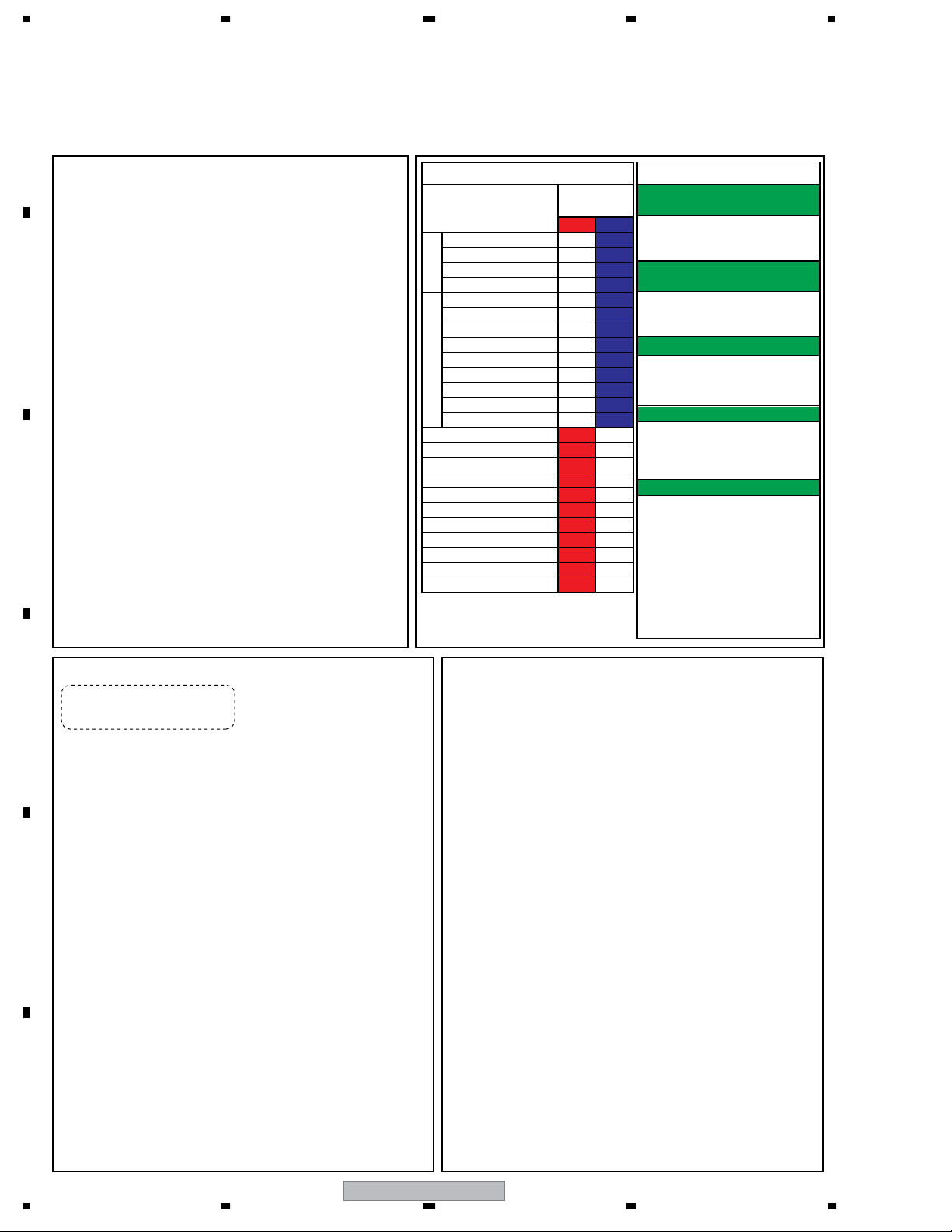
Quick Reference upon Service Visit 1
PD/SD
Item
Communication with the panel drive IC
Communication with the module IIC
DIGTAL-RST2
Panel high temperature
Panel section
Audio
Communication with the Module microcomputer
Main 3-wire serial communication
Main IIC communication
Communication with the Main microcomputer
FAN
Main section
Unit high temperature
Communication with the D-TUNER
MTB-RST2/RST4
POWER
SCAN
SCN-5V
Y-DRIVE
Y-DCDC
Y-SUS
ADRS
X-DRIVE
X-DCDC
X-SUS
UNKNOWN
Red 2
Red 3
Red 4
Red 5
Red 6
Red 7
Red 8
Red 9
Red 10
Red 11
Red 15
No. of LEDs
flashing
Red Blue
Blue 1
Blue 2
Blue 3
Blue 4
Blue 5
Blue 6
Blue 7
Blue 8
Blue 9
Blue 10
Blue 11
Blue 12
Blue 13
Change of settings
How to enter Factory mode using
the supplied remote control unit
In the same way as with the remote
control unit supplied with the 6thgeneration model
How to enter Integrator mode using
the supplied remote control unit
1 Enter the Standby mode.
2 Press [MENU].
3 Press [TV ].
Release TRAP SW-ERR
1 Enter the Factory mode.
2 Select the INITIALIZE mode.
3 Hold [DISPLAY] pressed for at least
5 seconds.
How to switch UART 1 (Integrator)
1 Enter the Integrator mode.
2 Display "OFF" using [\].
3 Change the communication speed
using [«], then [\].
How to switch UART 2 (During Standby)
1 Enter the Standby mode.
2
Hold [VOL +] or [VOL -] pressed for 3 seconds.
3
Hold [SPLIT] pressed for 3 seconds.
4-1 To set to 232C, press [ENTER].
5-2
To set to SR+, press [HOME MENU].
Note:
If switching is completed successfully,
the red LED will flash twice.
Note 1:
Use a remote control unit supplied with
the 6th-generation models or later.
Note 2:
Do not hold a key pressed for more
than 5 seconds.
How to locate several items on the Factory menu
{ } : Item on the Factory menu
D
E
F
[ ] : Key on the remote control unit
" " : Screen indication
1. Confirmation of accumulated power-on time and power-on
count
Select {INFORMATION} then {HOUR METER}.
(After entering Factory mode, press [«] four times.)
2. Confirmation of the Power-down and Shutdown histories
1 Panel system
PD: Select {PANEL FACTORY} then {POWER DOWN}.
(After entering Factory mode, press [MUTING] once, press
[ENTER], then press [«] three times.)
SD: Select {PANEL FACTORY} then {SHUT DOWN}.
(After entering Factory mode, press [MUTING] once, press
[ENTER], then press [«] four times.)
2 Main Assy
Select {INFORMATION} then {MAIN NG}.
(After entering Factory mode, press [«] three times.)
3. How to display the Mask indication
1 Mask indication in the panel side
1. Select {PANEL FACTORY} then {RASTER MASK SETUP}.
(After entering Factory mode, press [MUTING] once, press [ENTER],
then press [«] 8 times.)
2. Press [ENTER], then select a Mask indication, using [»] or [«].
2 Mask (SG screen) indication in the Main Assy (MAIN VDEC)
1. Select either Input 1 or 2 or 4, to which no signal is input (
2. Select {INITIALIZE} then {SG MODE}. Press [|]. (After entering
Factory mode, press [MUTING] three times, then press [«] once.)
Then, the indication at the lower right of the screen changes from
"OFF" to "ANA AD YCBCR".
3. You can change Mask patterns by pressing [«] to select {SG
PATTERN} then using [|] or [\].
Note: When you switch "SG MODE" routes, some displays become
monochrome, as they are in Y-signal only mode.
black screen
Adjustments and Settings after replacement of the
Assys (Procedures in Factory mode)
1. Digital Video Assy: Transfer of backup data
1 Select {PANEL FACTORY}, {ETC}, then {BACKUP DATA}. (After entering Factory
mode, press [MUTING] once, press [ENTER], press [«] seven times, then press
[ENTER].)
2 Select {TRANSFER}, using [\], then hold [SET] pressed for at least 5 seconds.
3 After transfer of backup data is completed, {ETC} is automatically selected, and the
LED on the front panel returns to normal lighting.
2. MAIN Assy (U): Execution of FINAL SETUP.
1 Select {INITIALIZE} then {FINAL SETUP}, then press [ENTER]. (After entering
Factory mode, press [MUTING] three times, then press [«] four times.)
2 Select "YES", using [\]. Then hold [ENTER] pressed for at least 5 seconds.
3 After "FINAL SETUP IS COMPLETE" is displayed on the screen, turn the POWER
switch of the main unit off.
3. POWER SUPPLY Unit: Clearance of the accumulated power-on count
and maximum temperature value
1 Select {PANEL FACTORY}, {ETC}, then {P COUNT INFO}. (After entering Factory
mode, press [MUTING] once, press [ENTER], press [«] seven times, press [ENTER],
then press [«] six times.)
2 Press [\] to select "CLEAR". Hold [SET] pressed for at least 5 seconds.
After clearance is completed, "ETC" is automatically selected. Clear the maximum
temperature value (MAX TEMP) in the same manner.
4. Other Assys: Clearance of the maximum temperature value
1 Select {PANEL FACTORY}, {ETC}, then {MAX TEMP}. (After entering Factory mode,
press [MUTING] once, press [ENTER], press [«] seven times, press [ENTER], then
press [«] seven times.)
2 Press [\] to select "CLEAR". Hold [SET] pressed for at least 5 seconds.
After clearance is completed, "ETC" is automatically selected.
).
6
PDP-4270XD
1234
Page 7
5678
Quick Reference upon Service Visit 2
Mode transition and structure of layers in Service Factory mode
Mode transition in Service Factory mode
INFORMATION mode
1. VERSION (1)
2. VERSION (2), (3)
3. MAIN NG
4. TEMPERATURE
5. HOUR METER
6. HDMI SIGNAL INFO1, 2
7. VDEC SIGNAL INFO 2
8. DTV TUNING STATUS 1, 2, 3
9. DTV TV-GUIDE BER
10. DEBUG INFO
PANEL FACTORY mode
1. PANEL INFORMATION
2. PANEL WORKS
3. POWER DOWN
4. SHUT DOWN
5. PANEL-1 ADJ
6. PANEL-2 ADJ
7. PANEL REVICE
8. ETC.
9. RASTER MASK SETUP
10. PATTEN MASK SETUP
11. COMBI MASK SETUP
Up
Down
• To shift to another mode, press [MUTING].
• To shift to another item in a specific mode,
press [»] or [«].
• To shift to the next nested layer below for an
item with a "(+)" indication, press [ENTER].
To return to the next nested layer above,
also press [ENTER].
INITIALIZE mode
1. SYNC DET
2. SG MODE
3. SG PATTERN
4. SIDE MASK LEVEL
5. FINAL SETUP
6. HMG/HG SERVICE MODE
7. CVT AUTO
8. HDMI INTR POSITION
OPTION mode
1. EDID WRITE MODE
2. ANTENNA MODE
3. AFT
Structure of Layers in Service Factory Mode
INFORMATION mode
1. VERSION (1) Flash Versions for PANEL system and MAIN system
2. VERSION (2) Flash Versions for DTV system
3. VERSION (3) Flash Versions for CCD ucom and HM
4. MAIN NG SD histories for MAIN (Going Clear model by SET key)
4-1. CLEAR Select Yes by [\] key \ pushing and hold [SET] key
5. TEMPERATURE TEMP 1, TEMP2 and FAN mode are displayed
6. HOUR METER Hour meter and number of Power ON are displayed
6-1. CLEAR Select Yes by [\] key \ pushing and hold [SET] key
7. HDMI SIGNAL INFO 1 For factory use
8. HDMI SIGNAL INFO 2 Signal info of HDMI are displayed ( Detail are on SM )
9. VDEC SIGNAL INFO For factory use
10. DTV TUNING STATUS 1 Detail information for DTV is displayed
11. DTV TUNING STATUS 2 Detail information for DTV is displayed
12. DTV TUNING STATUS 3 Detail information for DTV is displayed
13. DTV TV-GUIDE BER For production line use
14. DEBUG INFO For factory use
PANEL FACTORY mode Refer to [PANEL FACTORY MODE]
OPTION
1. EDID WRITE MODE For factory use
2. ANTENNA MODE For production line use
3. AFT For production line use
INITIALIZE
1. SYNC DET (+) For factory use
2. SG MODE SG signal from MAIN VDEC (
3. SG PATTERN For factory use
4. SIDE MASK LEVEL(+) For factory use
4-1. R MASK LEVEL
4-2. G MASK LEVEL
4-3. B MASK LEVEL
5. FINAL SETUP Set to Factory default settings (it should perform after
5-1. DATA RESET replacing a MAIN board )
6. HMG/HG SERVICE MODE Information for a USB device is displayed
6-1. MODE SIFT
7. CVT AUTO For factory use
8. HDMI INTR POSITION(+) For factory use
Composite signal is required
A
B
)
C
Structure of Layers in Panel Factory Mode 1
1. PANEL INFORMATION Version indication of the panel
2. PANEL WORKS Indications of the accumulated power-on time, pulse-meter
3. POWER DOWN Indication of the Power-down history
4. SHUT DOWN Indication of the Shutdown history
5. PANEL-1 ADJ (+)
1. X-SUS B
2. Y-SUS B
3. Y-SUSTAIL T1
4. Y-SUSTAIL T2 Modification not required because these items are basically
5. Y-SUSTAIL W for factory presetting
6. XY-RST W1
7. XY-RST W2
8. VOL SUS
9. VOL OFFSET Settings required after replacement of the panel
10. VOL RST P
11. SUS FREQ. For AM noise prevention (Depending on the mode,
6. PANEL-2 ADJ (+)
1. R-HIGH
2. G-HIGH
3 .B-HIGH Parameters for the WB adjustment of the panel, which are
4. R-LOW required during adjustment after panel replacement
5. G-LOW
6. B-LOW
7. ABL Setting of the power consumption. A setting table is
To "Structure of Layers in Panel Factory Mode 2"
count, and power-on count of the panel
brightness of the screen changes.)
available for each vertical signal.
Structure of Layers in Panel Factory Mode 2
7. PANEL REVISE (+)
R-LEVEL
G-LEVEL Items for use by engineers
B-LEVEL
8. ETC (+)
1. BACKUP DATA For transferring backup data (after replacement of
2. DIGITAL EEPROM To clear data of the digital video
3. PD INFO.
4. SD INFO. For clearance of data for the corresponding items.
5. HR-MTR INFO. The clearing method is the same: Select "CLEAR",
6. PM/B1-B5 using [\], then hold [SET] pressed for at least 5
7. P COUNT INFO. seconds. After clearance is completed, {ETC} is
8. MAX TEMP. automatically selected.
9. RASTER MASK SETUP (+)
1. MASK OFF
2. RST MASK 01 For use while Raster Mask (full mask) is displayed.
• • • • • Use [»] or [«] to select the type of mask.
25. RST MASK 24
10. PATTEN MASK SETUP (+)
1. MASK OFF
2. PTN MASK 01 For use while Pattern Mask is displayed. Use [»] or
• • • • • [«] to select the type of mask.
40. PTN MASK 39
11. COMBI MASK SETUP (+)
1. MASK OFF
2. CMB MASK 01 For use while Combination Mask is displayed.
• • • • • Use [»] or [«] to select the type of mask.
11. CMB MASK 10
the DIGITAL Assy)
D
E
56
PDP-4270XD
F
7
7
8
Page 8

1234
1.3 JIGS LIST
A
Cleaning
Name Part No. Remarks
Cleaning liquid GEM1004
Cleaning paper GED-008
Used to fan cleaning.
Refer to "2.4 CHASSIS SECTION (1/2).
CONTENTS
1. NOTES ON SERVICE VISIT.............................................................................................................................2
B
C
D
E
F
1.1 SAFETY INFORMATION ...........................................................................................................................2
1.2 QUICK REFERENCE UPON SERVICE VISIT........................................................................................... 6
1.3 JIGS LIST .................................................................................................................................................. 8
2. EXPLODED VIEWS AND PARTS LIST.......................................................................................................... 10
2.1 PACKING SECTION ................................................................................................................................10
2.2 REAR SECTION...................................................................................................................................... 12
2.3 FRONT SECTION.................................................................................................................................... 14
2.4 CHASSIS SECTION (1/2)........................................................................................................................16
2.5 CHASSIS SECTION (2/2)........................................................................................................................18
2.6 PANEL CHASSIS SECTION....................................................................................................................20
2.7 MULTI BASE SECTION........................................................................................................................... 22
2.8 PDP SERVICE PANEL ASSY 427 (AWU1208) .......................................................................................24
2.9 TABLE TOP STAND (PDP-4270XD ONLY)..............................................................................................25
3. PCB PARTS LIST ...........................................................................................................................................26
4. BLOCK DIAGRAM AND SCHEMATIC DIAGRAM..........................................................................................42
4.1 OVERALL WIRING DIAGRAM (1/2) ........................................................................................................42
4.2 OVERALL WIRING DIAGRAM (2/2) ........................................................................................................44
4.3 OVERALL BLOCK DIAGRAM (1/2) ......................................................................................................... 46
4.4 OVERALL BLOCK DIAGRAM (2/2) ......................................................................................................... 48
4.5 POWER SUPPLY UNIT............................................................................................................................ 49
4.6 42 X DRIVE, SUS CLAMP 1 and SUS CLAMP 2 ASSYS....................................................................... 50
4.7 42 Y DRIVE ASSY ................................................................................................................................... 51
4.8 POWER SUPPLY BLOCK of 42 X DRIVE and 42 Y DRIVE ASSYS....................................................... 52
4.9 42 SCAN A and 42 SCAN B ASSYS .......................................................................................................53
4.10 42 ADDRESS ASSY.............................................................................................................................. 54
4.11 42 DIGITAL ASSY..................................................................................................................................55
4.12 SIGNAL BLOCK DIAGRAM...................................................................................................................56
4.13 R07 DT ASSY (PDP-4270XD and PDP-427XD ONLY) ......................................................................... 58
4.14 POWER SUPPLY BLOCK of MAIN ASSY.............................................................................................59
4.15 42E AUDIO ASSY.................................................................................................................................. 60
4.16 POWER SUPPLY BLOCK of 42E AUDIO, LED IR and SIDE KEY ASSYS...........................................61
4.17 VOLTA GES.............................................................................................................................................62
4.18 WAVEFORMS........................................................................................................................................ 70
5. DIAGNOSIS.................................................................................................................................................... 74
5.1 TROUBLE SHOOTING............................................................................................................................74
5.2 DIAGNOSIS OF PD (POWER-DOWN)....................................................................................................92
5.3 DIAGNOSIS OF SD (SHUTDOWN).........................................................................................................96
5.4 INFORMATION ON SYMPTOMS THAT DO NOT CONSTITUTE FAILURE............................................98
6. DISASSEMBLY............................................................................................................................................... 99
6.1 PCB LOCATION....................................................................................................................................... 99
6.2 DISASSEMBLY ......................................................................................................................................100
7. ADJUSTMENT ............................................................................................................................................. 106
7.1 ADJUSTMENT REQUIRED WHEN THE SET IS REPAIRED OR REPLACED.....................................106
7.2 ADJUSTMENT REQUIRED WHEN PART IS REPLACED....................................................................107
7.3 BACKUP WHEN THE PANEL UNIT IS ADJUSTED .............................................................................. 108
7.4 HOW TO CLEAR HISTORY DATA.........................................................................................................111
7.5 ADJUSTMENT WHEN THE SERVICE PANEL ASSY IS REPLACED...................................................112
7.6 PROCEDURE WHEN REPLACING THE POWER SUPPLY UNIT........................................................ 114
8
1234
PDP-4270XD
Page 9

5678
8. SERVICE FACTORY MODE .........................................................................................................................115
8.1 OUTLINE OF THE SERVICE FACTORY................................................................................................115
8.1.1 SERVICE FACTORY MODE TRANSITION CHART.........................................................................115
8.1.2 HOW TO ENTER/EXIT SERVICE FACTORY MODE AND DO IT GO OUT ....................................115
8.1.3 STATE OF PRODUCT IN FACTORY MODE....................................................................................115
8.1.4 CORRESPONDENCE REMOTE CONTROL CODE.......................................................................116
8.1.5 FACTORY HIERARCHICAL TABLE .................................................................................................117
8.1.6 INDICATIONS IN SERVICE FACTORY MODE................................................................................118
8.2 SERVICE FACTORY MENU...................................................................................................................120
8.2.1 INFORMATION.................................................................................................................................120
8.2.2 PANEL FACTORY ............................................................................................................................128
8.2.3 OPTION............................................................................................................................................138
8.2.4 INITIALIZE........................................................................................................................................138
9. RS-232C .......................................................................................................................................................141
9.1 OUTLINE OF RS-232C COMMAND ......................................................................................................141
9.1.1 PREPARED TOOLS.........................................................................................................................141
9.1.2 USING RS-232C COMMANDS........................................................................................................141
9.1.3 COMMAND PROTOCOL..................................................................................................................142
9.1.4 COMMAND DEFINITION.................................................................................................................143
9.2 LIST OF RS-232C COMMANDS............................................................................................................145
9.3 OUTLINE OF EACH COMMANDS.........................................................................................................151
9.3.1 ACQUISITION OF PANEL STATUS • • • [QS1] ................................................................................151
9.3.2 ACQUISITION OF PANEL OPERATION DATA • • • [QS2]...............................................................152
9.3.3 ACQUISITION OF OTHER DATA ON THE PANEL • • • [QIP] ..........................................................153
9.3.4 ACQUISITION OF PANEL ADJUSTMENT DATA (COMMON DATA) • • • [QAJ] ..............................153
9.3.5 ACQUISITION OF ABL/WB ADJUSTMENT DATA • • • [QPW] ........................................................154
9.3.6 ACQUISITION OF PULSE METER VALUE • • • [QPM]...................................................................154
9.3.7 ACQUISITION OF PD LOGS • • • [QPD]..........................................................................................155
9.3.8 ACQUISITION OF SD LOGS • • • [QSD]..........................................................................................156
9.3.9 QS6..................................................................................................................................................157
9.3.10 QMT ...............................................................................................................................................157
9.3.11 QNG...............................................................................................................................................158
9.3.12 DRV................................................................................................................................................159
9.3.13 COMMANDS FOR PROHIBITION / PERMISSION OF DTV / HOMENET COMMUNICATION ....160
9.3.14 SETTING FOR FACTORY MODE PERMISSION / PROHIBITION • • • [FAY / FAN]......................161
9.3.15 BACKUP FUNCTION FOR ADJUSTMENT VALUE FOR THE MAIN UNIT • • • [FAJ / UAJ / CBU / BCP]161
10. GENERAL INFORMATION .........................................................................................................................162
10.1 POWER ON SEQUENCE.....................................................................................................................162
10.2 POWER SUPPLY TRANSITION STATUS.............................................................................................165
10.3 POWER ON/OFF FUNCTION FOR THE LARGE-SIGNAL SYSTEM..................................................166
10.4 LED INFORMATION.............................................................................................................................167
10.5 SPECIFICATION ABOUT THE THERMAL PROTECTION...................................................................168
10.6 PROCESSING IN ABNORMALITY ......................................................................................................169
11. SPECIFICATIONS.......................................................................................................................................171
11.1 SPECIFICATIONS................................................................................................................................171
11.2 ACCESSORIES....................................................................................................................................172
11.3 PANEL FACILITIES...............................................................................................................................173
12. IC INFORMATION.......................................................................................................................................178
A
B
C
D
56
PDP-4270XD
E
F
9
7
8
Page 10
1234
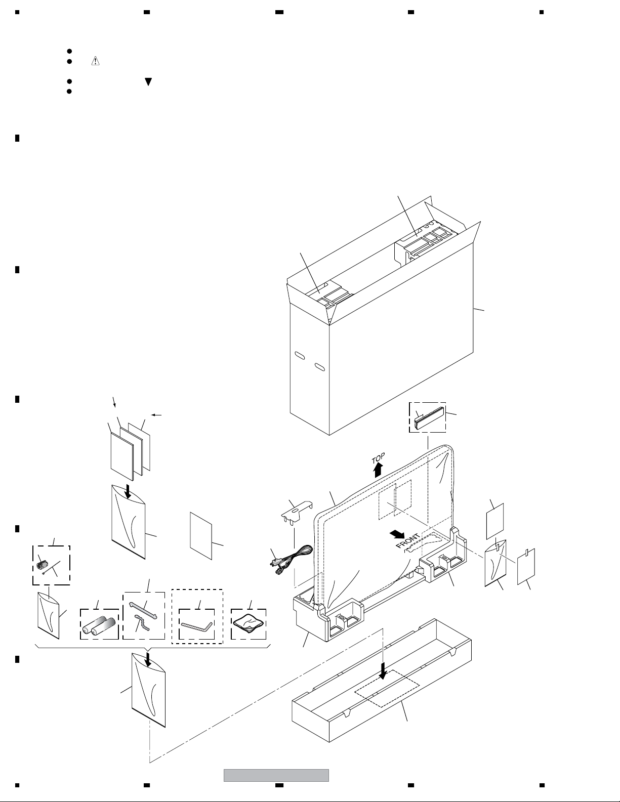
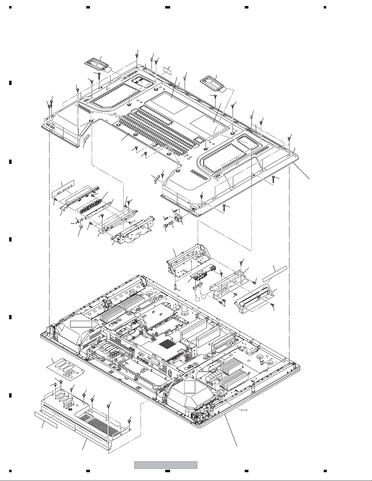
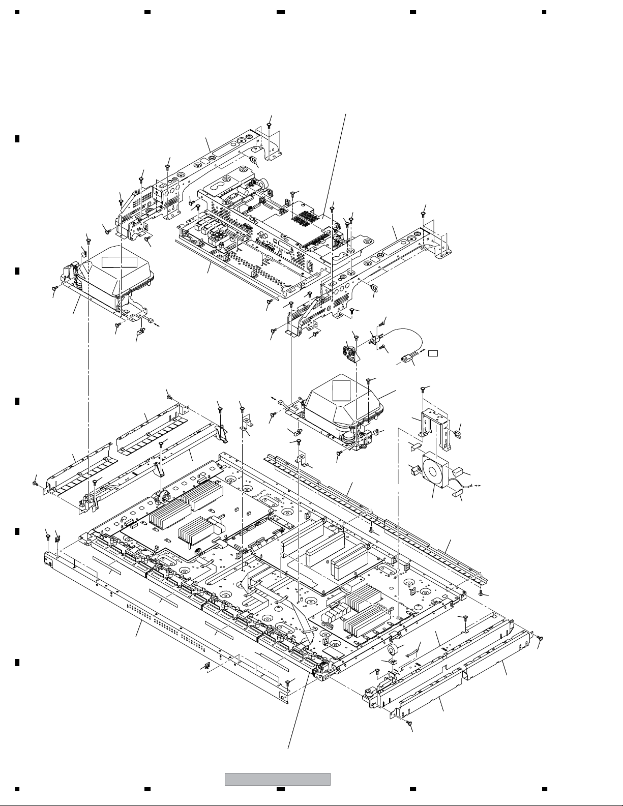
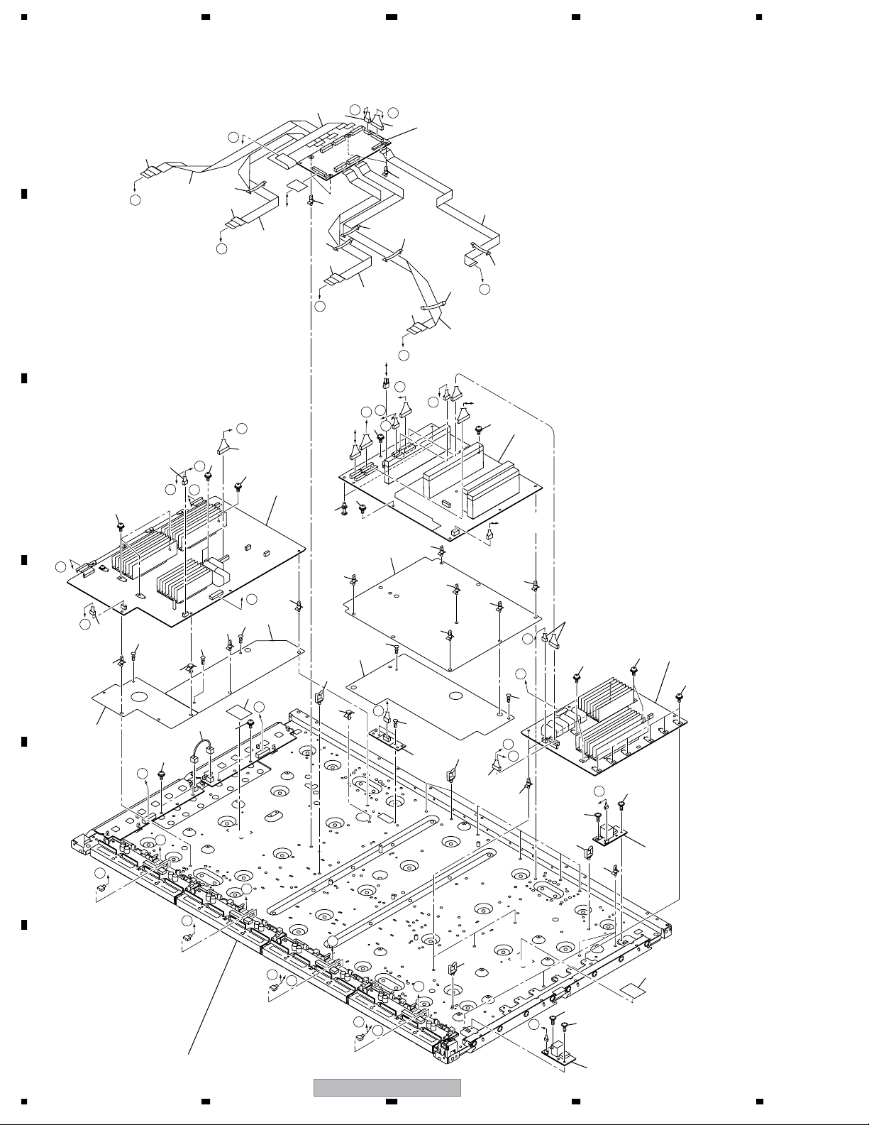
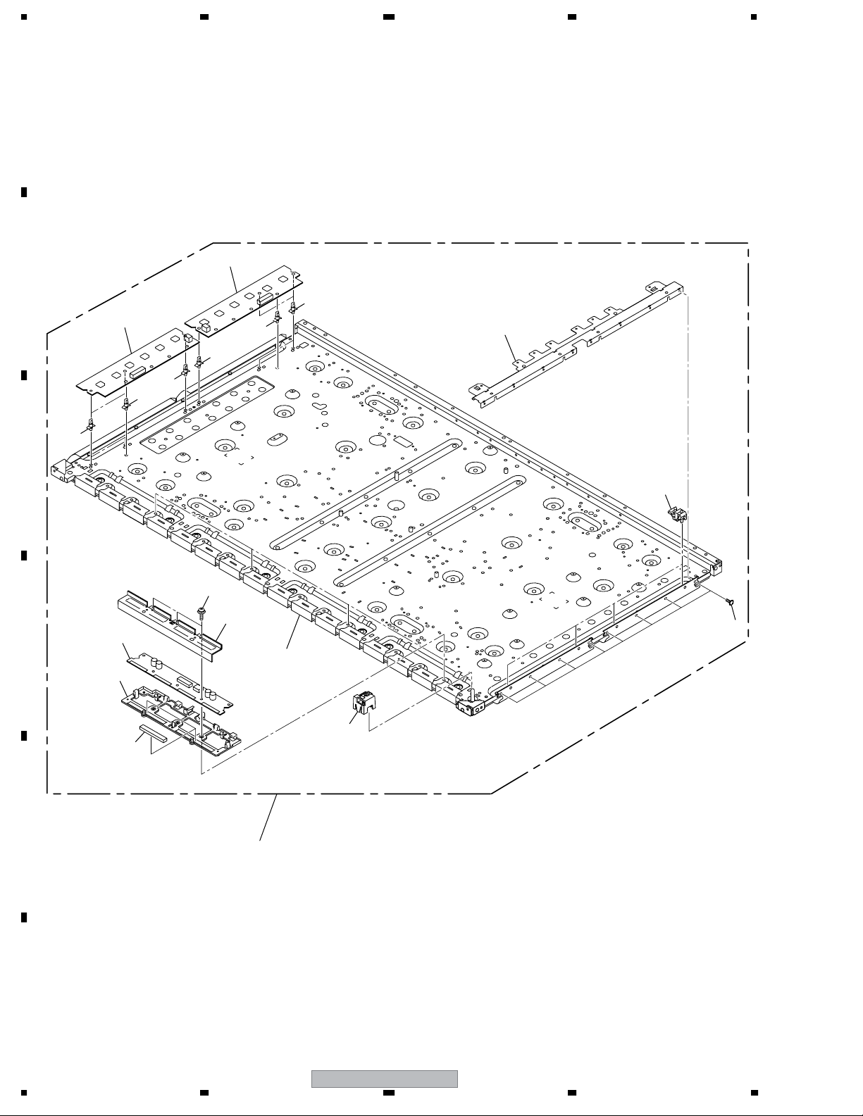
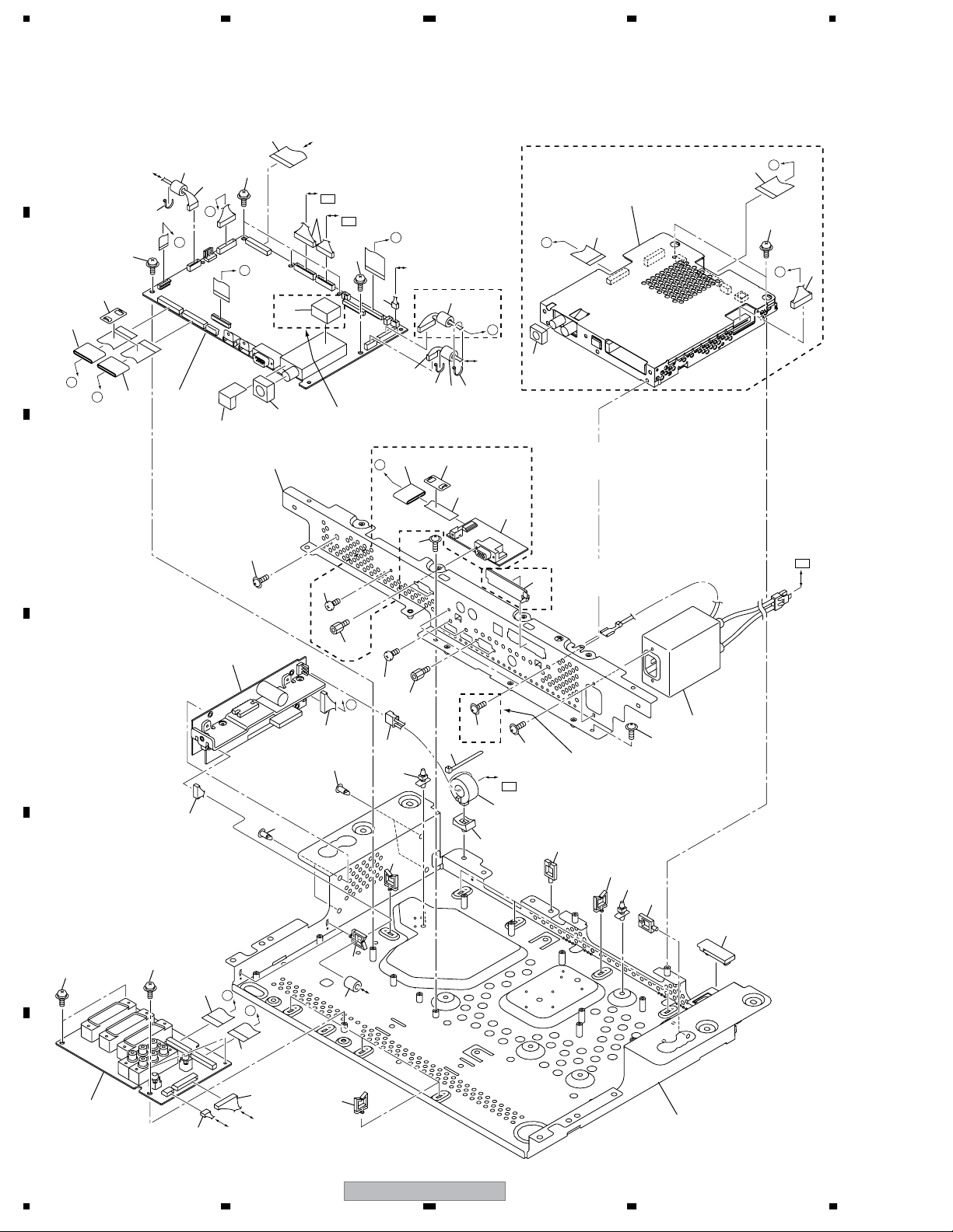
2. EXPLODED VIEWS AND PARTS LIST
NOTES:
Parts marked by "NSP" are generally unavailable because they are not in our Master Spare Parts List.
The mark found on some component parts indicates the importance of the safety factor of the part.
A
Therefore, when replacing, be sure to use parts of identical designation.
Screws adjacent to mark on product are used for disassembly.
For the applying amount of lubricants or glue, follow the instructions in this manual.
(In the case of no amount instructions, apply as you think it appropriate.)
2.1 PACKING SECTION
B
C
20
19
24
D
E
9
Ferrite core
Cable tie
18
PDP-4270XD/WYVIXK5, PDP-427XD/WYVIXK5,
PDP-427XA/WYVIXK5, WYV5
only
5
7
6
Speed clamp ×3
8
Bead band ×3
WYVIXK5 model
only
16
10
PDP-4270XD,
PDP-4270XA only
11
14
12
4
25
2
1
21
22
3
15
13
17
16
F
10
1234
PDP-4270XD
23
Page 11
>
>
5678
(1) PACKING SECTION PARTS LIST
No. Description Part No.
Mark
1Power Cord (2 m) ADG1214
2Power Cord Lid See Contrast table (2)
3 Remote Control Unit See Contrast table (2)
4 Battery Cover See Contrast table (2)
5 Operating Instructions See Contrast table (2)
(?????)
6 Operating Instructions See Contrast table (2)
(?????)
7 Block Diagram See Contrast table (2)
NSP 8 Dry Cell Battery (R06, AA) VEM1031
9Ferrite Core (L5321) ATX1039
10 Binder Assy AEC1908
NSP 11 Hexagonal Wrench (6 mm) See Contrast table (2)
12 Cleaning Cloth AED1285
13 Caution Card See Contrast table (2)
14 Cleaning Caution See Contrast table (2)
No. Description Part No.
Mark
NSP 15 Warranty Card ARY1114
16 Polyethylene Bag AHG1340
17 Polyethylene Bag AHG1326
18 Polyethylene Bag AHG1337
19 Pad (427 T-L) See Contrast table (2)
20 Pad (427 T-R) See Contrast table (2)
21 Pad (427 B-L) See Contrast table (2)
22 Pad (427 B-R) See Contrast table (2)
23 Under Carton (427) See Contrast table (2)
24 Upper Carton See Contrast table (2)
25 Mirror Mat See Contrast table (2)
A
B
(2) CONTRAST TABLE
PDP-4270XD/WYVIXK5, PDP-427XD/WYVIXK5, PDP-4270XA/WYVIXK5, WYV5, PDP-427XA/WYVIXK5 and
WYV5 are constructed the same except for the following:
Mark No. Symbol and Description
2Power Cord Lid AHC1087 AHC1087 AHC1087 AHC1087 AHC1085 AHC1085
3 Remote Control Unit AXD1515 AXD1532 AXD1541 AXD1540 AXD1541 AXD1540
4 Battery Cover AZA7424 AZN2626 AZA7424 AZN2626 AZA7424 AZN2626
5 Operating Instructions
(?????)
6 Operating Instructions
(?????)
7 Block Diagram ARY1189 ARY1189 ARY1189 ARY1189 Not used Not used
NSP 11 Hexagonal Wrench (6 mm) AEF1029 Not used AEF1029 Not used AEF1029 Not used
13 Caution Card ARM1310 ARM1310 ARM1310 ARM1310 ARM1232 ARM1232
14 Cleaning Caution PTK ARM1311 ARM1311 ARM1311 ARM1311 Not used Not used
14 Wiping Cloth Caution Not used Not used Not used Not used ARM1283 ARM1283
PDP-4270XD
/WYVIXK5
ARC1565 ARC1562 Not used ARC1564 Not used ARC1563
ARE1431 ARE1428 ARE1433 ARE1430 ARE1432 ARE1429
PDP-427XD
/WYVIXK5
PDP-4270XA
/WYVIXK5
PDP-427XA
/WYVIXK5
PDP-4270XA
/WYV5
PDP-427XA
/WYV5
C
D
E
19 Pad (427 T-L) AHA2554 AHA2554 AHA2554 AHA2554 AHA2534 AHA2534
20 Pad (427 T-R) AHA2555 AHA2555 AHA2555 AHA2555 AHA2535 AHA2535
21 Pad (427 B-L) AHA2600 AHA2600 AHA2600 AHA2600 AHA2592 AHA2592
22 Pad (427 B-R) AHA2601 AHA2601 AHA2601 AHA2601 AHA2593 AHA2593
23 Under Carton (427) AHD3496 AHD3496 AHD3496 AHD3496 AHD3471 AHD3471
24 Upper Carton AHD3514 AHD3515 AHD3497 AHD3517 AHD3513 AHD3516
25 Mirror Mat AHG1327 AHG1327 AHG1327 AHG1327 AHG1284 AHG1284
PDP-4270XD
56
7
8
F
11
Page 12
1234
2.2 REAR SECTION
A
12
29
33
33
29
33
37
31
33
8
16
13
31
12
8
37
15
33
31
33
B
8
37
11
18
30
8
33
33
11
25
24
34
C
33
3
22
MAIN
CN4010
(Accessory of No.3)
Binder
35
33
5
33
1
35
32
10
7
32
17
28
14
6
33
29
29
27
35
35
D
4
2
26
33
23
9
A
B
33
36
33
36
20
33
36
B
A
33
E
33
35
TANSHI
33
F
19
21
12
1234
PDP-4270XD
CN9001, CN9002
Refer to
"2.3 FRONT SECTION".
Page 13
5678
(1) REAR SECTION PARTS LIST
No. Description Part No.
Mark
1 SIDE KEY Assy AWW1133
2 SIDE Assy AWW1162
3 Filter CTX1054
4 Side Input Panel (E) ANC2418
5 Function Button Base ANG2923
No. Description Part No.
Mark
21 Terminal Panel B See Contrast table (2)
22 Function Button Panel AMB2906
23 Side Input Cover AMB2911
24 Function Button (E) AAC1565
25 Function Button Sheet (E) AAK2896
A
6 Side Input Shield ANK1834
7 Function Button Shield ANK1835
8 Rear Case Cushion AEB1439
NSP 9 PCB Support AEC1288
10 Locking Card Spacer AEC2019
11 Protection Sheet C AED1300
12 Inner Grip Assy AMR3434
NSP 13 Name Label See Contrast table (2)
14 Coil Spring ABH1125
15 Bolt Caution Label See Contrast table (2)
16 Serial Seal AAX3143
17 Power Button AAD4145
18 Terminal Display Label A See Contrast table (2)
19 Terminal Display Label C See Contrast table (2)
20 Terminal Display Label B See Contrast table (2)
26 Input Cover Label E See Contrast table (2)
27 Rear Case (427) ANE1655
28 Power Button Holder AMR3539
29 Screw (3 x 40P) ABA1332
30 Screw ABA1341
31 Screw (4 x 18) ABA1353
32 Screw BPZ30P140FTB
33 Screw AMZ30P060FTB
34 Screw AMZ30P080FTC
35 Screw APZ30P080FTB
36 Screw BPZ30P080FTB
37 Screw TBZ40P080FTB
B
C
(2) CONTRAST TABLE
PDP-4270XD/WYVIXK5, PDP-427XD/WYVIXK5, PDP-4270XA/WYVIXK5, WYV5, PDP-427XA/WYVIXK5 and
WYV5 are constructed the same except for the following:
Mark No. Symbol and Description
NSP 13 Name Label AAL2801 AAL2804 AAL2803 AAL2806 AAL2802 AAL2805
15 Bolt Caution Label AAX3005 AAX3005 AAX3005 AAX3005 Not used Not used
15 Caution Label Not used Not used Not used Not used AAX3117 AAX3117
18 Terminal Display Label A AAX3343 AAX3337 AAX3399 AAX3398 AAX3344 AAX3332
19 Terminal Display Label C AAX3340 AAX3339 AAX3340 AAX3339 AAX3340 AAX3339
20 Terminal Display Label B AAX3419 AAX3417 AAX3419 AAX3417 AAX3419 AAX3417
21 Terminal Panel B ANC2429 ANC2403 ANC2429 ANC2403 ANC2429 ANC2403
26 Input Cover Label E AAX3397 AAX3396 AAX3397 AAX3396 AAX3376 AAX3375
PDP-4270XD
/WYVIXK5
PDP-427XD
/WYVIXK5
PDP-4270XA
/WYVIXK5
PDP-427XA
/WYVIXK5
PDP-4270XA
/WYV5
PDP-427XA
/WYV5
D
E
F
56
PDP-4270XD
13
7
8
Page 14
1234
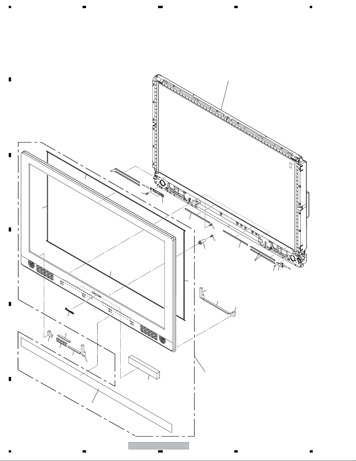
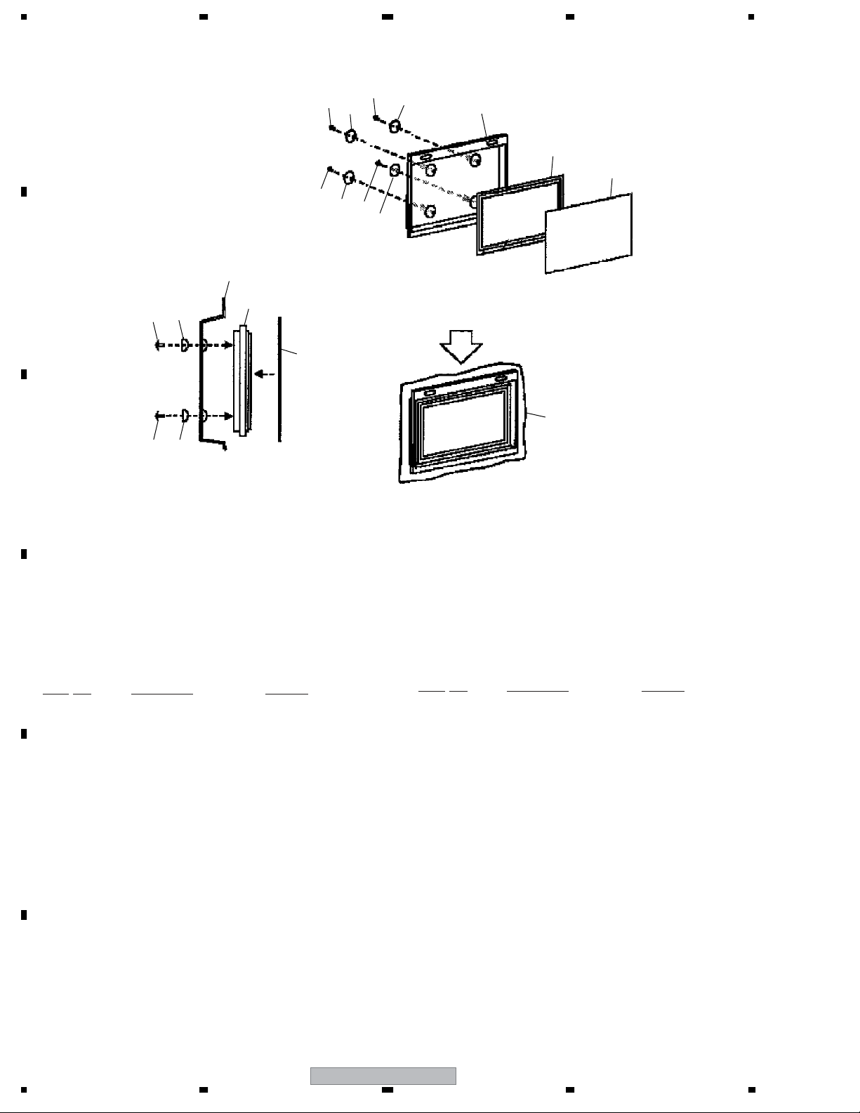
2.3 FRONT SECTION
A
B
Refer to
"2.4 CHASSIS SECTION (1/2)".
8
17
MAIN
CN4006
1
8
18
16
15
11
4
8
8
8
MAIN
2
6
5
CN4010
12
C
11
D
13
7
12
E
F
14
5
3
7
4
10
9
14
PDP-4270XD
1234
Page 15
5678
(1) FRONT SECTION PARTS LIST
No. Description Part No.
Mark
1 42 & 60 LED Assy AWW1134
2 LED IR Assy AWW1136
3 Blind Cushion (427HX) AEB1443
4 Speaker Cushion AEB1452
5 Speaker Cushion S See Contrast table (2)
6 Nyron Rivet AEC1671
7 Insulation Sheet B AED1284
8 Insulation Sheet AED1289
9 Reinforcement Frame AMR3620
10 Front Case Assy See Contrast table (2)
A
11 Panel Cushion V (42) AED1301
12 Panel Cushion H (42) AED1309
13 Pioneer Name Plate AAM1096
14 Punching Sheet See Contrast table (2)
15 Front Collar AMR3541
16 Screw (3 x 30P) ABA1350
17 Screw (M3 x 4) ABA1354
18 Screw APZ30P080FTB
19 Front Case Cushion See Contrast table (2)
20 IR Block Cushion AEB1465
21 IR Blind Sheet AAX3455
(2) CONTRAST TABLE
PDP-4270XD/WYVIXK5, PDP-427XD/WYVIXK5, PDP-4270XA/WYVIXK5, WYV5, PDP-427XA/WYVIXK5 and
WYV5 are constructed the same except for the following:
Mark No. Symbol and Description
5 Speaker Cushion S Not used AEB1460 Not used AEB1460 Not used AEB1460
10 Front Case Assy AMB2971 AMB2968 AMB2972 AMB2969 AMB2972 AMB2969
14 Punching Sheet AAS1015 AAS1014 AAS1015 AAS1014 AAS1015 AAS1014
19 Front Case Cushion (42B) AEB1464 AEB1462 AEB1464 AEB1462 AEB1464 AEB1462
PDP-4270XD
/WYVIXK5
PDP-427XD
/WYVIXK5
PDP-4270XA
/WYVIXK5
PDP-427XA
/WYVIXK5
PDP-4270XA
/WYV5
PDP-427XA
/WYV5
B
C
D
56
PDP-4270XD
E
F
15
7
8
Page 16
1234
2.4 CHASSIS SECTION (1/2)
A
35
31
31
B
31
32
22
31
36
31
10
26
19
35
36
Refer to
"2.7 MULTI BASE SECTION".
35
31
36
11
35
31
31
31
31
30
30
42E AUDIO
CN3753
31
1
C
31
24
42E AUDIO
CN3753
30
29
14
24
29
13
D
30
32
23
29
7
16
31
30
16
30
27
30
15
35
19
34
3
POWER
12
P3
6
29
28
34
AC inlet
32
2
22
18
18
18
MAIN
CN4009
4
18
33
15
25
E
33
25
29
8
9
25
25
20
23
32
29
21
5
30
13
14
F
30
Refer to
"2.5 CHASSIS SECTION (2/2)".
16
PDP-4270XD
1234
Page 17

5678
CHASSIS SECTION (1/2) PARTS LIST
No. Description Part No.
Mark
1 Speaker Box Assy L AMW1010
2 Speaker Box Assy R AMW1011
3Power Switch (S1) ASG1092
4Fan Motor 80 x 25L AXM1059
5Ferrite Core ATX1044
6 Housing Wire (42, 50)(J103) ADX3320
7Front Chassis VL (427) AMA1020
8Front Chassis VR (427) AMA1021
9Front Chassis H Assy (427) ANA2047
10 Sub Frame Assy L (427) ANA1943
>
>
>
A
11 Sub Frame Assy R (427) ANA1944
12 Fan Holder ANG2833
13 Panel Holder V1 (427) ANG2920
14 Panel Holder V2 (427) ANG2921
15 Panel Holder H (427) ANG2922
16 Multi Base Holder ANG2937
17 • • • • •
18 Floating Rubber 80 AEB1427
19 Wire Saddle AEC1745
20 Ferrite Core Holder AEC1818
21 Flat Clamp AEC1879
22 Locking Wire Saddle AEC1948
23 Mini Clamp AEC2090
24 Re-use Wire Saddle AEC2091
25 Address Gasket (42) ANK1877
26 Gasket D ANK1840
27 Switch Holder AMR3540
28 Re-use Wire Saddle AEC1945
29 Screw ABA1351
30 Screw ABZ30P080FTC
B
C
D
31 Screw AMZ30P060FTB
32 Screw APZ30P080FTB
33 Screw BBZ30P060FTC
34 Screw BPZ30P080FTB
35 Screw TBZ40P080FTB
36 Screw ABA1364
56
PDP-4270XD
E
F
17
7
8
Page 18
1234
2.5 CHASSIS SECTION (2/2)
A
H
9
G
22
F
5
19
8
12
26
28
26
14
26
26
E
8
26
A
10
8
MAIN
CN4001
11
B
28
26
8
B
C
13
42E AUDIO
D
CN3751
I
J
F
MAIN
CN4008
37
I
17
C
20
36
36
J
K
L
36
4
23
K
37
33
M
28
H
32
N
21
D
34
28
34
27
28
34
28
34
30
25
Q
28
28
28
29
31
L
16
37
37
M
27
G
24
6
25
MAIN
CN4002
28
15
37
7
AC inlet,
Power switch
28
O
P
28
18
R
36
E
36
3
37
34
37
O
36
E
N
A
25
1
28
B
K
C
25
Q
R
F
Q
D
36
R
P
37
29
Refer to
18
"2.6 PANEL CHASSIS SECTION".
PDP-4270XD
2
1234
Page 19

5678
CHASSIS SECTION (2/2) PARTS LIST
No. Description Part No.
Mark
1 SUS CLAMP 1 Assy AWW1022
2 SUS CLAMP 2 Assy AWW1023
3 42 X DRIVE Assy AWW1196
4 42 Y DRIVE Assy AWV2400
5 42 DIGITAL Assy AWW1240
6 SENSOR Assy AWW1140
7POWER SUPPLY Unit AXY1153
8Ferrite Core ATX1048
9 Flexible Cable (J201) ADD1429
10 Flexible Cable (J202) ADD1430
>
A
11 Flexible Cable (J203) ADD1431
12 Flexible Cable (J204) ADD1432
13 Flexible Cable (J205) ADD1433
14 Flexible Cable (J206) ADD1434
15 6P Housing Wire (J118) ADX3118
16 3P Housing Wire (J119) ADX3122
17 9P Housing Wire (J101) ADX3318
18 8P&5/4P Housing Wire (J102) ADX3319
19 14P Housing Wire (J105) ADX3323
20 6P/4P Housing Wire (J108) ADX3326
21 4P Housing Wire (J109) ADX3327
22 5P Housing Wire (J110) ADX3328
23 Spacer AEC1065
24 Nyron Rivet AEC1671
25 Wire Saddle AEC1745
26 Flat Clamp AEC1879
27 PCB Support AEC1938
28 Re-use PCB Spacer AEC2087
29 Drive Silicone Sheet AEH1095
30 Power Supply Sheet B (507) AMR3555
B
C
D
31 Y Drive Protection Sheet A AMR3632
32 Y Drive Protection Sheet B AMR3633
33 Power Supply Sheet (427) A AMR3648
34 Rivet A BEC1158
35 • • • • •
36 Screw ABA1351
37 Screw ABA1368
56
PDP-4270XD
E
F
19
7
8
Page 20
1234
2.6 PANEL CHASSIS SECTION
A
5
B
4
8
8
8
8
8
7
8
C
10
13
6
D
E
3
2
11
14
9
1
12
F
20
1234
PDP-4270XD
Page 21
5678
(1) PANEL CHASSIS SECTION PARTS LIST
No. Description Part No.
Mark
NSP 1 Panel Chassis (427S) Assy See Contrast table (2)
NSP 2 Plasma Panel (42DC) Assy AWU1161
NSP 3 42 ADDRESS Assy AWV2335
NSP 4 42 SCAN A Assy AWW1182
NSP 5 42 SCAN B Assy AWW1183
6 Address Heatsink ANH1644
7 Conductive Plate X ANG2791
8 Re-use PCB Spacer AEC2087
9 Address Silicone A AEH1093
10 Conductive Plate Holder AMR3446
A
11 Address Holder Assy AMR3460
12 Screw ABA1364
13 Screw BBB30P120FNI
14 Tube Cover (FT) AMR3557
(2) CONTRAST TABLE
PDP-4270XD/WYVIXK5, PDP-427XD/WYVIXK5, PDP-4270XA/WYVIXK5, WYV5, PDP-427XA/WYVIXK5 and
WYV5 are constructed the same except for the following:
Mark No. Symbol and Description
NSP 1 Panel Chassis (427S) Assy AWU1185 AWU1185 AWU1185 AWU1185 AWU1207 AWU1207
PDP-4270XD
/WYVIXK5
PDP-427XD
/WYVIXK5
PDP-4270XA
/WYVIXK5
PDP-427XA
/WYVIXK5
PDP-4270XA
/WYV5
PDP-427XA
/WYV5
B
C
D
56
PDP-4270XD
E
F
21
7
8
Page 22
1234
2.7 MULTI BASE SECTION
A
B
C
SIDE KEY CN9501
LED IR CN9701
(Accessory of No.42)
Binder
47
31
8
B
C
8
13
42
D
21
47
A
F
42 DIGITAL
CN3001
POWER
P8
17
POWER
P9
47
29
H
Fan
PDP-4270XD,
PDP-427XD only
42
5
F
15
PDP-427XD only
H
9
47
16
G
41
PDP-4270XD,
G
20
1
39
40
(Accessory of No.42)
PDP-4270XD,
PDP-427XD only
36
Binder
7
D
Binder
42
(Accessory of No.42)
31
38
PDP-427XD,
PDP-427XA only
14
3
47
46
43
PDP-4270XD,
34
PDP-427XD only
POWER
P3
4
44
46
18
25
44
24
45
POWER
P5
43
PDP-4270XD,
PDP-427XD only
10
43
D
A
19
33
6
23
33
30
27
26
30
25
26
E
28
47
47
12
B
C
42
30
Speaker
11
F
2
32
SIDE
CN9205
SIDE
CN9207
22
30
35
22
PDP-4270XD
1234
Page 23
5678
(1) MULTI BASE SECTION PARTS LIST
No. Description Part No.
Mark
1 MAIN Assy See Contrast table (2)
2TANSHI Assy See Contrast table (2)
3 PC Assy See Contrast table (2)
4 42E AUDIO Assy AWW1185
5 R07 DT Assy See Contrast table (2)
>
>
>
>
>
No. Description Part No.
Mark
26 Wire Saddle AEC1745
27 Ferrite Core Holder AEC1818
28 Clamp AEC1884
29 3P Housing Wire (J127) ADX3421
30 Re-use Wire Saddle AEC1945
A
6Ferrite Core ATX1044
7Ferrite Core See Contrast table (2)
8Ferrite Core ATX1064
9 Flexible Cable (J214) See Contrast table (2)
10 AC Inlet (CN1) AKP1301
11 Flexible Cable (J210) ADD1441
12 Flexible Cable (J211) ADD1441
13 Flexible Cable (J207) ADD1445
14 Flexible Cable (J213) See Contrast table (2)
15 Flexible Cable (J215) See Contrast table (2)
16 12P Housing Wire (J126) See Contrast table (2)
17 13P&11P Housing Wire (J106) ADX3324
18 3P Housing Wire (J107) ADX3325
19 11P Housing Wire (J111) ADX3329
20 6P Housing Wire (J113) ADX3331
21 7/6/4P Housing Wire (J114) ADX3332
22 14P Housing Wire (J116) ADX3334
23 8/4P Housing Wire (J117) ADX3336
24 Binder AEC-093
25 Locking Card Spacer AEC1429
31 Ferrite Stopper AEC1981
32 5P Housing Wire (J125) ADX3388
33 Locking Card Spacer AEC2019
34 POD Cover See Contrast table (2)
35 Multi Base Assy See Contrast table (2)
36 Terminal Panel A See Contrast table (2)
37 • • • • •
38 Gasket N See Contrast table (2)
39 Gasket EA ANK1855
40 Gasket EB ANK1899
41 Gasket ED See Contrast table (2)
42 Filter CTX1054
43 Screw AMZ30P060FTB
44 Hex. Head Screw BBA1051
45 Screw See Contrast table (2)
46 Screw BMZ30P060FTB
47 Screw PMB30P080FNI
B
C
(2) CONTRAST TABLE
PDP-4270XD/WYVIXK5, PDP-427XD/WYVIXK5, PDP-4270XA/WYVIXK5, WYV5, PDP-427XA/WYVIXK5 and
WYV5 are constructed the same except for the following:
Mark No. Symbol and Description
1 MAIN Assy AWV2320 AWV2318 AWV2320 AWV2318 AWV2320 AWV2318
2TANSHI Assy AWW1178 AWW1161 AWW1178 AWW1161 AWW1178 AWW1161
3 PC Assy Not used AWW1163 Not used AWW1163 Not used AWW1163
5 R07 DT Assy AWE1311 AWE1311 Not used Not used Not used Not used
7Ferrite Core Not used ATX1063 Not used ATX1063 Not used ATX1063
9 Flexible Cable (J214) ADD1450 ADD1450 Not used Not used Not used Not used
14 Flexible Cable (J213) Not used ADD1452 Not used ADD1452 Not used ADD1444
15 Flexible Cable (J215) ADD1451 ADD1451 Not used Not used Not used Not used
16 12P Housing Wire (J126) ADX3390 ADX3390 Not used Not used Not used Not used
34 POD Cover AMR3542 AMR3542 Not used Not used Not used Not used
35 Multi Base Assy ANA1952 ANA1952 ANA2019 ANA2019 ANA2019 ANA2019
36 Terminal Panel A ANC2400 ANC2398 ANC2415 ANC2399 ANC2415 ANC2399
>
38 Gasket N ANK1776 ANK1776 Not used Not used Not used Not used
>
41 Gasket ED ANK1863 ANK1863 Not used Not used Not used Not used
45 Screw
PDP-4270XD
/WYVIXK5
BBZ30P060FTB BBZ30P060FTB
PDP-427XD
/WYVIXK5
PDP-4270XA
/WYVIXK5
Not used Not used Not used Not used
PDP-427XA
/WYVIXK5
PDP-4270XA
/WYV5
PDP-427XA
/WYV5
D
E
F
56
PDP-4270XD
23
7
8
Page 24
1234
2.8 PDP SERVICE PANEL ASSY 427 (AWU1208)
4
A
4
23
4
23
23
4
23
22
1
21
B
23
4
23
4
C
D
22
1
21
PDP SERVICE PANEL ASSY 427 (AWU1208) PARTS LIST
Mark No. Description Part No.
NSP 1 Panel Chassis (427) Assy AWU1171
2 Caution Label AAX3031
NSP 3 Drive Voltage Label ARW1097
4 Screw PMB50P150FTC
5 Screw ABA1351
20
Mark No. Description Part No.
16 Pad 42SINGLE(B-L) AHA2552
17 Pad 42SINGLE(B-R) AHA2553
18 Upper Carton (42SINGLE) AHD3480
19 Under Carton (42SINGLE) AHD3481
20 Polyethylene Bag AHG1381
6 Wire Saddle AEC1745
E
7 PCB Support AEC1938
8 Vinyl Bag S AHG1338
NSP 9 Vinyl Bag AHG1340
10 Y Drive Protection Sheet A AMR3632
11 Power Sheet (427) A AMR3648
12 Address Gasket (42) ANK1877
13 Rivet A BEC1158
14 Pad 42SINGLE(T-L) AHA2550
15 Pad 42SINGLE(T-R) AHA2551
F
24
1234
21 Packing Sheet AHG1386
22 Tray (FT) AHX1158
23 Cup Spacer (15) ANG2936
PDP-4270XD
Page 25
5678
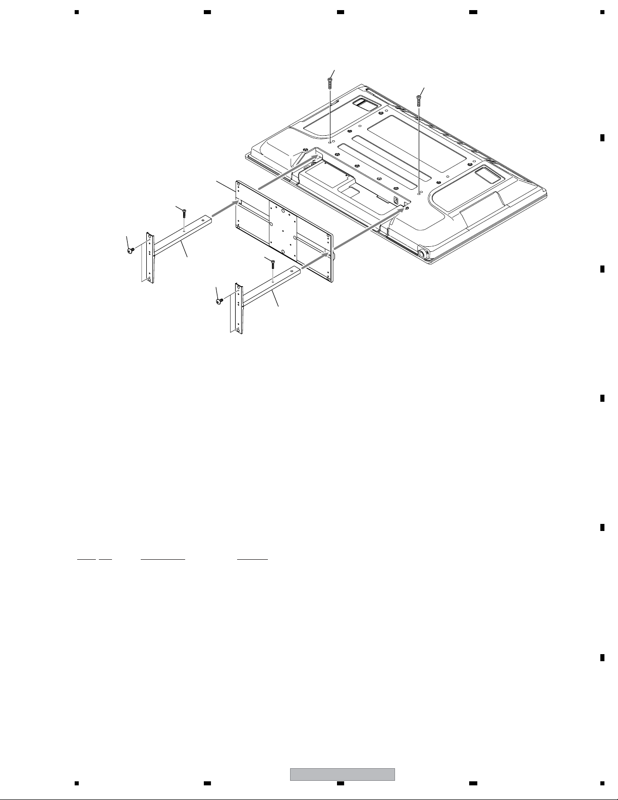
2.9 TABLE TOP STAND (PDP-4270XD ONLY)
5
5
2
4
3
1
3
4
1
A
B
C
TABLE TOP STAND PARTS LIST
Mark No. Description Part No.
1 Stand Pipe Assy AXY1144
2 Base Cover Assy AXY1143
3 Screw ABA1357
4 Screw (HEX) SMZ80H300FTC
5 Screw (HEX) ABA1365
D
E
F
56
PDP-4270XD
25
7
8
Page 26
1234
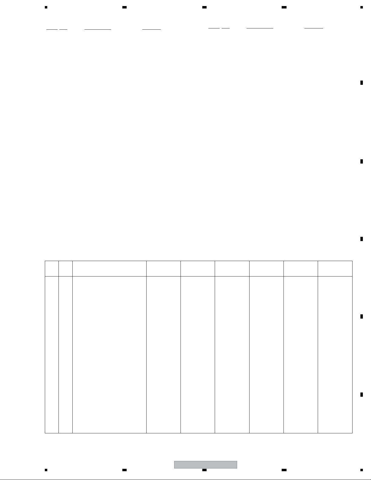
3. PCB PARTS LIST
>
NOTES:
A
Parts marked by "NSP" are generally unavailable because they are not in our Master Spare Parts List.
The mark found on some component parts indicates the importance of the safety factor of the part.
Therefore, when replacing, be sure to use parts of identical designation.
When ordering resistors, first convert resistance values into code form as shown in the following examples.
Ex.1 When there are 2 effective digits (any digit apart from 0), such as 560 ohm and 47k ohm (tolerance is shown by J=5%,
and K=10%).
560 Ω
47k Ω
0.5 Ω
1 Ω
56 x 10
47 x 10
R50
1R0
1
3
561
473
RD1/4PU J
RD1/4PU J
RN2H K
RS1P K
561
473
R50
1R0
Ex.2 When there are 3 effective digits (such as in high precision metal film resistors).
5.62k Ω
77
77
LIST OF WHOLE PCB ASSEMBLIES
B
Mark Symbol and Description
1..R07 DT ASSY AWE1311 AWE1311 Not used Not used Not used Not used
1..MAIN ASSY AWV2320 AWV2318 AWV2320 AWV2318 AWV2320 AWV2318
NSP 1..IO ASSY AWV2321 AWV2319 AWV2321 AWV2319 AWV2321 AWV2319
2..TANSHI ASSY AWW1161 AWW1178 AWW1161 AWW1178 AWW1161 AWW1178
2..SIDE ASSY AWW1162 AWW1162 AWW1162 AWW1162 AWW1162 AWW1162
2..PC ASSY Not used AWW1163 Not used AWW1163 Not used AWW1163
NSP 1..42E AUDIO ASSY AWV2369 AWV2369 AWV2369 AWV2369 AWV2369 AWV2369
C
2..SIDE KEY ASSY AWW1133 AWW1133 AWW1133 AWW1133 AWW1133 AWW1133
2..42 & 60 LED ASSY AWW1134 AWW1134 AWW1134 AWW1134 AWW1134 AWW1134
2..LED IR ASSY AWW1136 AWW1136 AWW1136 AWW1136 AWW1136 AWW1136
2..42E AUDIO ASSY AWW1185 AWW1185 AWW1185 AWW1185 AWW1185 AWW1185
1
5621
PDP-4270XD
/WYVIXK5
PDP-427XD
/WYVIXK5
PDP-4270XA
/WYVIXK5
RN1/4PC F562 x 10
PDP-427XA
/WYVIXK5
5621
PDP-4270XA
/WYV5
PDP-427XA
/WYV5
NSP 1..42 X DRIVE ASSY AWV2399 AWV2399 AWV2399 AWV2399 AWV2399 AWV2399
2..SUS CLAMP 1 ASSY AWW1022 AWW1022 AWW1022 AWW1022 AWW1022 AWW1022
2..SUS CLAMP 2 ASSY AWW1023 AWW1023 AWW1023 AWW1023 AWW1023 AWW1023
2..42 X DRIVE ASSY AWW1196 AWW1196 AWW1196 AWW1196 AWW1196 AWW1196
1..42 Y DRIVE ASSY AWV2400 AWV2400 AWV2400 AWV2400 AWV2400 AWV2400
NSP 1..42 DIGITAL ASSY AWV2435 AWV2435 AWV2435 AWV2435 AWV2435 AWV2435
D
E
2..SENSOR ASSY AWW1140 AWW1140 AWW1140 AWW1140 AWW1140 AWW1140
2..42 DIGITAL ASSY AWW1240 AWW1240 AWW1240 AWW1240 AWW1240 AWW1240
NSP 1..PANEL CHASSIS (427S) ASSY AWU1185 AWU1185 AWU1185 AWU1185 AWU1185 AWU1185
NSP 2..42 ADDRESS ASSY AWV2335 AWV2335 AWV2335 AWV2335 AWV2335 AWV2335
NSP 2..42 SCAN ASSY AWV2362 AWV2362 AWV2362 AWV2362 AWV2362 AWV2362
NSP 3..42 SCAN A ASSY AWW1182 AWW1182 AWW1182 AWW1182 AWW1182 AWW1182
NSP 3..42 SCAN B ASSY AWW1183 AWW1183 AWW1183 AWW1183 AWW1183 AWW1183
1..POWER SUPPLY UNIT AXY1153 AXY1153 AXY1153 AXY1153 AXY1153 AXY1153
F
26
1234
PDP-4270XD
Page 27
5678
77
77
CONTRAST OF PCB ASSEMBLIES
MAIN ASSY
AWV2320 and AWV2318 are constructed the same except for the following :
Mark Symbol and Description AWV2320 AWV2318
IC5103 Not used TVP5150AM1PBS-K
IC5404 Not used BR24L02FJ
IC8305 Not used TC74VHC00FTS1
Q5402 Not used HN1K02FU
Q5408 Not used UMD2N
Q5414 Not used RN1902
Q8302 Not used 2SA1586
Q8303, Q8304 Not used DTC124EUA
Q8311 Not used 2SJ461A
D5402 Not used 1SS301
D5408 Not used UDZS6R8(B)
D8301 - D8303 Not used 1SS355
C4922, C4932, C4933, C5101, C5102, C5103 Not used CKSRYB105K10
C5104, C5105 Not used CCSSCH100D50
C5117, C5123, C5125, C5126, C5449 - C5451 Not used CKSSYF104Z16
C5121, C5122, C5124, C8320 Not used CKSSYB104K10
C5452, C8319 Not used DCH1201
C5453 Not used CCSSCH101J50
R4031 Not used RS1/16S0R0J
R4056, R8344 Not used RS1/16SS0R0J
R4057 RS1/16SS0R0J Not used
R4728, R4729, R4904, R4905, R4910 Not used RS1/16SS220J
R4809, R4810 Not used RS1/16SS562J
R4964, R4965, R4966 Not used RS1/16S75R0F
R5103 Not used ACN1246
A
B
C
R5121, R8347, R8359 Not used RS1/16SS332J
R5122, R5419, R8476 Not used RS1/16SS103J
R5124, R5125, R5126 Not used RS1/16SS470J
R5147 Not used RAB4CQ220J
R5421, R8364 Not used RS1/16SS101J
R5422 Not used RS1/16SS473J
R5423, R5424 Not used RS1/16SS100J
R5433, R8353 Not used RS1/16SS102J
R8354 Not used RS1/16SS122J
R8355 Not used RS1/16SS104J
R8356, R8358 Not used RS1/16S122J
R8357 Not used RS1/16S220J
R8376 RS1/10S0R0J Not used
R8379, R8380 RS1/16SS223J Not used
R8477, R8480 RS1/16SS103J Not used
X5101 CRYSTAL Not used ASS1189
CN4018 12P FFC CONNECTOR Not used AKM1233
JA5402 HDMI CONNECTOR Not used AKP1278
D
E
56
PDP-4270XD
F
27
7
8
Page 28
1234
TANSHI ASSY
AWW1178 and AWW1161 are constructed the same except for the following :
Mark Symbol and Description AWW1178 AWW1161
A
B
77
77
Mark No. Description Part No.
C
Q9012 Not used HN1A01FU
Q9015 Not used 2SC4116
Q9016 Not used 2SD2114K
F9001 - F9007 Not used CTF1557
C9037 Not used CCG1205
C9022, C9025 Not used CKSRYB105K10
C9010 - C9012 Not used CKSSYB471K50
C9023, C9026 Not used CKSRYB102K50
C9043 Not used CKSRYB224K10
JA9005 2P PINJACK AKB1331 AKB1340
JA9002 Not used VKN1449
JA9004 Not used AKN1081
PCB PARTS LIST FOR PDP-427XD/WYVIXK5 UNLESS OTHER WISE NOTED
Mark No. Description Part No.
R07 DT ASSY
MISCELLANEOUS
9 XNG1002
11 ANG2673
12-15 SCREW PMZ20P100FNI
16-18 SCREW ABZ30P060FTC
[TUNER BLOCK]
C1018,1027,1029,1050 CEHVKW470M16
C1019 CEHVKW100M50
C1020 CEHVKW100M16
C1025,1026,1030-1035 CKSRYB104K16
C1028,1038,1042,1046 CCG1205
C1036 CKSRYB105K10
C1037,1039,1049,1053 CKSRYB104K16
C1043,1044 CCSRCJ3R0C50
C1045 CKSRYB103K50
C1051 CCG1205
>
>
SEMICONDUCTORS
IC1000 UPC3221GV
IC1001 STV0361L
Q1001 2SC2412K
Q1002 DTC124EUA
Q1003,1004 RK7002
D
>
D1000 SM15T6V8A
D1001 1SS355
MISCELLANEOUS
L1000 XTX1005
L1002 LCYAR82J2520
L1004 XTX1003
L1200 XTX1001
F1000 XTF1002
F1001,1003-1010 VTF1091
E
F1012-1014,1100,1101 VTF1091
F1202-1204 VTF1091
X1100 CRYSTAL (27 MHz) XSS1010
All Resistors RS1/16S###J
>
FU1200 CHIP FUSE (0.25A) XEK1003
>
M1000 FRONT END XXF1007
CAPACITORS
C1001-1003,1017,1022 CKSRYB104K16
C1004,1055 CEHVKW101M6R3
C1010 CEHVKW2R2M50
C1013,1021,1040,1041 CKSRYB103K50
F
C1015 CKSRYB102K50
C1054 BCG1050
C1056,1057 CEHVKW470M16
C1058-1062 CKSRYB104K16
C1102 CEHVKW331M6R3
[DEMUX BLOCK]
SEMICONDUCTORS
IC2000 STI5517DW AL
IC2001 SN74LVU04APW
IC2002 TC74VHC08FTS1
Q2000 2SC4081
D2000 DA204U
D2001 UDZS8R2(B)
D2002 HVU307
D2005,2009 RB501V-40
MISCELLANEOUS
L2000 XTX1003
F2000-2003 VTF1091
CRYSTAL RESONAT OR (27 MHz)
X2000
X2001 CRYSTAL OSCILLATOR ASS1172
VA2002 VARISTOR
BSS1112
AVR-M1608C120MT2AB
RESISTORS
R2010,2018,2042 RAB4C103J
R2070,2071 RAB4CQ220J
Other Resistors RS1/16S###J
28
PDP-4270XD
1234
Page 29

5678
Mark No. Description Part No.
CAPACITORS
C2000,2026,2030 CCSRCH101J50
C2001 CKSRYB471K50
C2002,2003,2005,2006 CKSRYF104Z16
C2004 CKSRYF474Z16
C2007 CCSRCH471J50
Mark No. Description Part No.
CAPACITORS
C4000,4002 CCG1205
C4001,4014,4032,4033 CKSRYB103K50
C4003,4005,4017,4018 CKSRYF104Z16
C4004 CEHVKW2R2M50
C4006 CKSRYB102K50
A
C2008,2017,2020,2021 CKSRYB102K50
C2009 CCSRCH330J50
C2011,2012 CCSRCH390J50
C2013 CKSRYB105K10
C2014,2016 CCSRCH100D50
C2015 CKSRYF105Z10
C2018,2019,2022-2025 CKSRYF104Z16
C2027,2029,2042,2046 CKSRYF223Z50
C2028,2035,2037-2041 CKSRYF104Z16
C2032-2034,2036 CEHVKW470M16
C2043-2045,2047,2048 CKSRYF104Z16
[MEMORY BLOCK]
SEMICONDUCTORS
IC3000,3003 K4S281632I-UC75
IC3002 XGC1003
MISCELLANEOUS
L3003 XTX1003
L3005 XTX1001
RESISTORS
R3004-3014 RAB4CQ470J
Other Resistors RS1/16S###J
CAPACITORS
C3000,3003,3007,3008 CKSRYF104Z16
C3001,3002,3004,3014 CKSRYF223Z50
C3010 CEHVKW470M16
C3012,3017,3020-3022 CKSRYF104Z16
C3015,3018,3019,3023 CKSRYF223Z50
C4007,4013 CCSRCH220J50
C4008,4009 CCSRCH121J50
C4010,4011,4042 CCSRCH101J50
C4012,4022,4023,4029 CEHVKW470M16
C4019,4102-4104 CEHVKW100M16
C4021,4024,4043 CKSRYF104Z16
C4038 CKSRYB103K50
C4039 CEHVKW470M16
C4040,4041 CKSRYB105K10
C4105-4107 CKSRYF104Z16
C4108-4113 CEHVKW100M16
[CI BLOCK]
SEMICONDUCTORS
IC5000 ST890CDR
IC5001 CIMAXSP2L
IC5002 TC74LCX245FTS1
IC5003,5004 TC74LCX373FT
Q5000 2SC4081
Q5001 DTA143EUA
Q5002 DTC124EUA
MISCELLANEOUS
CN5000 PCMCIA CONNECTOR XKP1003
RESISTORS
R5014,5019,5022,5024 RAB4CQ470J
R5030,5032,5036-5038 RAB4CQ470J
R5045-5050 RAB4CQ470J
Other Resistors RS1/16S###J
B
C
D
C3024 CKSRYF223Z50
[AV BLOCK]
SEMICONDUCTORS
IC4000 CS4334-KS
IC4001 SN74LVU04APW
IC4002 RC4558D
IC4003 CS8406CZZ
IC4100 PCM1803DB
Q4001,4002 2SC4081
MISCELLANEOUS
F4000,4100 FERRITE CORE VTF1091
JA4000 OPTICAL OUT MOD. GP1FM513TZ
X4000 CRYSTAL (12.288 MHz) XSS1006
CN4000 40P CONNECTOR AKM1348
RESISTORS
R4042,4045,4046 RS1/16S2000F
Other Resistors RS1/16S###J
56
CAPACITORS
C5001 CKSRYB105K10
C5003,5004,5006 CKSRYF104Z16
C5005,5100 CEHVKW470M16
C5008-5013 CKSRYF104Z16
[POWER BLOCK]
SEMICONDUCTORS
IC6001 M5291FP
IC6002 BA05FP
IC6003 FPF2003
IC6200 TC74LCX245FTS1
IC6300 SN74LVC1G08DCK
Q6001,6009,6011,6200 DTC124EUA
Q6003,6005,6010 DTA143EUA
Q6006 2SB1188
Q6008 TPC8209
Q6100 2SC4081
D6001 RSX201L-30
D6003,6100-6102 1SS355
D6103 UDZS30(B)
PDP-4270XD
E
F
29
7
8
Page 30

1234
Mark No. Description Part No.
MISCELLANEOUS
L6000 LCYAR82J2520
L6001,6100,6101 XTH1001
A
F6000 FERRITE CORE VTF1091
CN6000 12P CONNECTOR AKM1298
CN6003 50P CONNECTOR AKM1349
RESISTORS
R6012-6014 RAB4C2R2J
R6031 RAB4C221J
R6204,6205 RAB4CQ101J
Other Resistors RS1/16S###J
CAPACITORS
C6000,6026,6104-6106 CEHVKW331M6R3
C6001,6011,6013-6015 CEHVKW470M16
B
C6002,6035 CKSRYF223Z50
C6003,6005,6006,6012 CKSRYF104Z16
C6004 CEHVKW100M50
C6008,6016 CKSRYF474Z16
C6010 CCSRCH331J50
C6017,6028,6036,6042 CEHVKW101M6R3
C6018,6020,6021,6025 CKSRYF104Z16
C6019,6023,6100 CEHVKW470M16
C6022 CKSRYB103K50
C6027 CCSRCH101J50
C6029,6030,6033,6038 CKSRYF104Z16
C
C6031 CEHVKW2R2M50
C6044 CEHVKW101M6R3
Mark No. Description Part No.
[REG 0 BLOCK]
SEMICONDUCTORS
IC4101,4114,4115 S-1132B18-U5
IC4102 LTC3414EFE
IC4103 LTC3412EFE
IC4104,4111,4113 NJM2846DL3-05
IC4105 S-1170B25UC-OTK
IC4106 S-1170B15UC-OTA
IC4107 NJM2846DL3-33
IC4108 NJM2846DL3-18
IC4109,4110 PQ090DNA1ZPH
Q4101,4103 RN1902
Q4102 HN1C01FU
Q4104 DTC124EUA
Q4105,4106 UPA1917TE
Q4107-4109 2SC4116
Q4110 2SD2114K
D4101-4110,4112-4118 1SS355
D4111,4119,4120,4122 1SS357
D4121 1SS355
MISCELLANEOUS
L4101,4103 BTX1042
L4102,4105-4107 BTX1039
L4108 ATH1208
L4109 ATH1194
F4101,4102 VTF1080
C6102 CCG1191
C6200,6300 CKSRYF104Z16
MAIN ASSY
[BOARD IF BLOCK]
D
SEMICONDUCTORS
IC4001-4005 TC74VCX541FT
Q4001,4002,4005 DTC124EUA
Q4003,4004 RN2902
MISCELLANEOUS
L4001-4006 BTX1042
>
F4001-4010 CTF1557
CN4001,4004,4005 50P CONNECTOR AKM1349
CN4006 PLUG(6P) KM200NA6
CN4013 50P CONNECTOR PBF AKM1353
CN4014 40P CONNECTOR PBF AKM1354
E
RESISTORS
R4001 RAB4CQ470J
R4021-4024 BCN1067
R4030,4035 RS1/16S0R0J
Other Resistors RS1/16SS###J
RESISTORS
R4113,4134-4136,4140 RS1/10S0R0J
R4119,4131,4146 RS1/16SS3003F
R4120 RS1/16SS2003F
R4123,4159 RS1/16SS1502F
R4124 RS1/16SS6202F
R4133 RS1/16SS1503F
R4148,4164-4170,4173 RS1/10S0R0J
Other Resistors RS1/16SS###J
CAPACITORS
C4018,4101,4103,4106 CKSRYB105K10
C4102,4104,4105,4107 DCH1201
C4108 CKSRYB105K10
C4109,4111-4113,4116 DCH1201
C4110,4117 CCSSCH101J50
C4114,4118 BCG1050
C4119,4127,4131,4134 DCH1201
C4121,4140,4153 CKSSYB104K10
C4122,4129 CCSSCH220J50
C4123,4124,4126,4130 DCH1165
C4132 ACH1421
C4135,4138,4143-4146 DCH1201
C4136,4137,4141,4142 BCG1059
C4139 CCSRCH471J50
C4147 CCSRCH102J50
CAPACITORS
C4001-4003,4007,4009 CKSSYF104Z16
C4004 CCSSCH101J50
C4006,4036,4039 DCH1201
C4008 DCH1165
F
C4014 CKSSYF104Z16
C4033,4051 CKSRYF104Z50
C4048-4050 CCSSCH470J50
30
1234
C4150 ACH1429
C4151 CKSSYB102K50
C4154 CKSSYF104Z16
C4155 CKSSYB103K16
C4165 DCH1201
PDP-4270XD
Page 31

5678
Mark No. Description Part No.
[ATUNER BLOCK]
SEMICONDUCTORS
IC4501 MSP3417G
Q4501 DTC124EUA
Q4503 UMD2N
Q4504 HN1B04FU
Q4505 2SC4116
Q4506 2SA1586
Q4508 HN1C01FU
D4501 UDZS24(B)
D4502,4505 UDZS8R2(B)
MISCELLANEOUS
L4501-4503 BTH1119
F4501-4503 VTF1080
X4501 CRYSTAL (18.432 MHz) ASS1196
>
U4501 FRONT END (EU) AXF1172
Mark No. Description Part No.
R4645,4647,4648 RAB4CQ103J
R4649 RS1/10S0R0J
Other Resistors RS1/16SS###J
CAPACITORS
C4603,4612,4646,4650 DCH1201
C4604 CKSSYB103K16
C4605,4606 CCSSCH220J50
C4607 CKSSYB102K50
C4610,4611,4613,4615 CKSSYF104Z16
C4617,4619,4621,4623 CKSSYF104Z16
C4625,4627,4629,4631 CKSSYF104Z16
C4633,4635,4636,4639 CKSSYF104Z16
C4642,4644,4648,4651 CKSSYF104Z16
C4647 CKSSYB104K10
C4652,4655,4657,4659 CKSSYF104Z16
A
B
RESISTORS
R4517 RS1/16S330J
R4522,4523 RS1/16S470J
Other Resistors RS1/16SS###J
CAPACITORS
C4501-4503 CKSRYF104Z50
C4504 CKSRYB682K50
C4505,4512 CCSSCH5R0D50
C4506 CKSSYB103K16
C4507,4508,4513,4514 CCSSCH100D50
C4509,4515,4518 CKSSYB102K50
C4511 CCSSCH560J50
C4520 CEHVKW101M6R3
C4521,4523,4525,4528 DCH1201
C4527,4529,4536,4537 CKSSYF104Z16
C4530,4532-4534,4538 DCH1201
C4539,4543 CKSSYF104Z16
C4541 DCH1201
[TEXT UCOM BLOCK]
SEMICONDUCTORS
IC4601 SDA6000
IC4602 HY57V641620ETP-H
IC4603 AGC1020
IC4606 TC74LCX125FT
IC4607 TC7SH04FUS1
Q4601,4602 UMD2N
D4601 1SS355
D4602 UDZS12(B)
D4603 UDZS3R0(B)
D4604 UDZS3R9(B)
MISCELLANEOUS
X4601 CRYSTAL ASS1193
RESISTORS
R4601 ACN1251
R4602-4606,4608,4625 BCN1067
R4627,4650 RS1/16S0R0J
R4640 RAB4CQ470J
R4644,4646 RAB4CQ680J
[AV SW BLOCK]
SEMICONDUCTORS
IC4701 R2S11002AFT
IC4702,4706 NJM12904V
IC4703 PCM1803DB
IC4704 NJU26901E2
IC4705 PCM1754DBQ
Q4701,4702,4721 UMD2N
Q4703-4708,4715 2SA1586
Q4711,4712,4716,4717 2SC4116
Q4718 DTA124EUA
Q4719,4720 2SC4116
Q4722,4723 HN1B04FU
D4701,4702,4704,4705 1SS301
D4703 1SS355
MISCELLANEOUS
X4701 CRYSTAL ASS1204
RESISTORS
R4736,4737 RS1/16S5600F
R4739,4741 RS1/16S1800F
R4794,4795,4851,4852 RS1/16S182J
R4815-4817 RS1/10S0R0J
R4849 RS1/16S472J
R4853 RS1/16S222J
R4860,4861,4863,4865 RS1/16S102J
R4866 RAB4CQ470J
Other Resistors RS1/16SS###J
CAPACITORS
C4701,4723,4725,4731 CKSSYF104Z16
C4702-4708,4710-4717 CKSR YB105K10
C4718,4719 CCSRCH181J50
C4720,4721 CCSRCH681J50
C4722,4724,4726,4733 DCH1201
C4727,4730 CKSSYB104K10
C4728,4729 CKSRYB221K50
C4732,4744,4751,4752 CKSSYF104Z16
C4734,4749,4750,4757 DCH1201
C4735,4736,4739-4742 CKSRYB105K10
C
D
E
F
56
PDP-4270XD
31
7
8
Page 32

1234
Mark No. Description Part No.
C4737 ACG1122
C4745,4767,4768 DCH1165
C4753 ACH1394
C4754,4755,4759,4760 CKSRYB105K10
A
C4756,4761,4763,4764 CKSSYF104Z16
C4758,4762,4765 DCH1201
C4766,4772-4774 CKSSYF104Z16
C4769-4771 DCH1201
C4775,4776 CKSSYB681K50
C4777,4779 CKSSYB152K50
C4778 CCSSCH221J50
C4780-4783 CKSRYB105K10
C4784,4785 CCSRCH331J50
B
[RGB SW BLOCK]
Mark No. Description Part No.
CAPACITORS
C5106,5107,5136,5140 CKSSYB103K16
C5108,5109 CCSSCH8R0D50
C5113,5118,5119 DCH1201
C5120,5129,5131,5133 CKSSYF104Z16
C5127,5128,5130,5132 CKSSYB104K10
C5134,5135,5137,5139 CKSSYB104K10
C5138,5144,5155-5165 CKSSYF104Z16
C5141-5143,5145,5151 CKSSYB104K10
C5150 CKSSYB103K16
C5153,5191 CKSSYB104K10
[ADC BLOCK]
SEMICONDUCTORS
IC5301 AD9985KSTZ-110
SEMICONDUCTORS
IC4901 R2S11001FT
Q4901-4903,4905 2SA1586
Q4904,4906 HN1B04FU
D4901-4903 UDZS4R7(B)
RESISTORS
R4913-4918 RS1/16SS3301F
R4919,4926,4930 RS1/16SS5600F
R4921,4928,4932 RS1/16SS75R0F
C
R4925 RAB4CQ102J
Other Resistors RS1/16SS###J
CAPACITORS
C4901-4903 CKSRYB105K10
C4904 CCSRCH331J50
C4905 CCSRCH680J50
C4906-4910,4912-4915 CKSSYB103K16
C4911,4935 CKSRYB474K10
C4916,4923,4924,4926 CKSSYF104Z16
C4917-4921 CKSSYB103K16
C4925,4927 DCH1201
D
C4928-4931 CKSSYF104Z16
[VDEC BLOCK]
SEMICONDUCTORS
IC5101 UPD64015AGM-UEU
IC5102 EDS1616AGTA-75-E
MISCELLANEOUS
F5101 EMI FILTER CCG1162
X5102 CRYSTAL ASS1191
E
RESISTORS
R5101,5102,5104,5105 ACN1246
R5106,5107 BCN1067
R5108-5110 RS1/16S0R0J
R5118-5120 RS1/16SS470J
R5133-5135 RS1/16SS2000F
R5136-5138 RS1/16SS220J
R5140 RS1/16S334J
R5148 RAB4CQ220J
R5149-5151,5153,5155 RS1/10S0R0J
Other Resistors RS1/16SS####D
F
RESISTORS
R5301-5303 BCN1067
R5305 RS1/16SS2701F
R5307,5308,5312,5313 RS1/16SS470J
R5310,5311 RS1/10S0R0J
Other Resistors RS1/16S###J
CAPACITORS
C5301 CKSSYB823K10
C5302 CKSSYB822K16
C5303-5305 CKSSYB473K16
C5307,5313 CKSSYB104K10
C5308-5312,5314-5316 CKSSYF104Z16
C5318,5319 CKSSYF104Z16
[HDMI BLOCK]
SEMICONDUCTORS
IC5401 SII9023CTU
IC5402 PCM1754DBQ
IC5403 BR24L02FJ-W
Q5401 HN1K02FU
Q5407 UMD2N
Q5413 RN1902
D5401 1SS301
D5407 UDZS6R8(B)
MISCELLANEOUS
JA5401 HDMI CONNECTOR AKP1278
X5401 CRYSTAL ASS1192
RESISTORS
R5401-5403 BCN1071
R5413,5429 RS1/10S0R0J
R5450 RAB4CQ473J
R5451 RAB4CQ100J
R5452,5455 RAB4CQ103J
R5454 RAB4CQ470J
Other Resistors RS1/16SS###J
CAPACITORS
C5401,5402 CCSSCH120J50
C5403,5404,5408,5410 CKSSYF104Z16
C5405,5407,5473 DCH1201
C5406 CCSSCH101J50
C5412,5414,5416,5418 CKSSYF104Z16
32
PDP-4270XD
1234
Page 33

5678
Mark No. Description Part No.
C5423,5426-5428,5430 CKSSYF104Z16
C5432,5434,5436,5438 CKSSYF104Z16
C5440,5442,5444,5445 CKSSYF104Z16
C5447,5448,5455,5457 CKSSYF104Z16
C5458,5460,5462,5464 CKSSYF104Z16
C5466,5468,5469,5471 CKSSYF104Z16
C5472 CKSSYF104Z16
[DSEL BLOCK]
SEMICONDUCTORS
IC8001 PD6523A
IC8002 TC74LCX125FT
IC8003 TC74VCX574FT
MISCELLANEOUS
L8001-8003 BTX1042
>
F8004 ATX1058
X8001 CRYSTAL ASS1194
Mark No. Description Part No.
MISCELLANEOUS
L8201-8205 BTX1042
RESISTORS
R8201-8205 ACN1246
R8206-8208,8255 ACN1251
R8209 RS1/10S0R0J
R8214,8215,8248 RAB4CQ103J
R8225,8245 BCN1071
R8246 BCN1073
R8249 RAB4CQ680J
Other Resistors RS1/16SS###J
CAPACITORS
C8202 CKSSYB102K50
C8203-8205 DCH1201
C8221-8234,8239 CKSSYF104Z16
[IF UCOM BLOCK]
A
B
RESISTORS
R8001,8002 ACN1251
R8003,8008 RAB4CQ680J
R8004-8006 BCN1071
R8009-8011 BCN1067
R8026,8027 RAB4CQ101J
Other Resistors RS1/16SS###J
CAPACITORS
C8002 CKSSYB102K50
C8003,8005,8014-8020 CKSSYF104Z16
C8025,8027 CKSSYF104Z16
C8026 DCH1201
[IP BLOCK]
SEMICONDUCTORS
IC8101 PE5504B
IC8102,8103 EDS6432AFTA-75-E
MISCELLANEOUS
L8101-8104 BTX1042
RESISTORS
R8101-8104,8106-8110 BCN1067
R8105 BCN1071
R8111,8116 ACN1246
R8112-8115,8117 ACN1251
R8123 RAB4CQ103J
R8135 RAB4CQ470J
R8136 RAB4CQ101J
Other Resistors RS1/16SS###J
SEMICONDUCTORS
IC8301 AGC1016
IC8302 PST9230N
IC8303 TC74VHC08FTS1
IC8304 TC7W126FU
IC8306 MAX3232CPW
IC8307 TC74VHC125FTS1
IC8308 TC74VHC00FTS1
Q8301,8315 DTA124EUA
Q8306,8308 DTC124EUA
Q8307,8312 2SA1586
Q8309,8313 2SC4116
Q8310,8314 HN1C01FU
D8304,8305 1SS355
MISCELLANEOUS
X8301 CERAMIC RESONATOR ASS1168
X8302 CRYSTAL OSCILLATOR ASS1172
CN8301 9P D-SUB SOCKET AKP1213
RESISTORS
R8307 RAB4CQ473J
R8348,8351,8352 RAB4CQ103J
R8376 RS1/10S0R0J
Other Resistors RS1/16SS###J
CAPACITORS
C8301 CKSSYB472K25
C8302,8303 CCSSCH220J50
C8305,8312 CCSRCH471J50
C8306-8311,8322,8323 CKSSYF104Z16
C8313-8317,8321,8324 CKSSYB104K10
C
D
E
CAPACITORS
C8101 CKSSYB102K50
C8112-8115,8117-8120 CKSSYF104Z16
C8134-8145 CKSSYF104Z16
[MULTI BLOCK]
SEMICONDUCTORS
IC8201 PEG121B
IC8202 AGC1019
IC8203 TC74VHC08FTS1
56
[MAIN UCOM BLOCK]
SEMICONDUCTORS
IC8401 MB91305PMC-G-BND
IC8402 AGC1018
IC8403 PST3628UR
IC8407 PQ200WNA1ZPH
IC8409 BR24L64F-W
IC8410,8411 TC74VHC125FTS1
PDP-4270XD
F
33
7
8
Page 34

1234
Mark No. Description Part No.
Q8401 2SJ461A
Q8402 DTC124EUA
Q8403,8405 HN1K02FU
D8401 1SS355
A
D8402 SML-311UT
Mark No. Description Part No.
R8885,8893 RS1/16S680J
R8898,8915-8917,8922 RS1/16S75R0F
R9008 RS1/16S4701F
R9037,9038,9040 RS1/16S75R0F
R9046-9048 RS1/16S75R0F
D8403-8405 1SS301
MISCELLANEOUS
X8401 CERAMIC OSCILLATOR CSS1616
CN8401 50P CONNECTOR PBF AKM1353
RESISTORS
R8401,8402 ACN1248
R8408,8467 RAB4CQ101J
R8454,8455 RS1/16S0R0J
B
R8464 RS1/16S4701F
R8465 RS1/16S1801F
R8466 RS1/16S1001F
R8484 RS1/16SS5602F
R8485 RS1/16SS2002F
Other Resistors RS1/16SS###J
CAPACITORS
C8402-8405,8408-8413 CCSSCH470J50
C8414 CKSSYB102K50
C8416,8426 CCSSCH120J50
C8417 CKSSYB472K25
C
C8418,8443 CKSSYB103K16
C8421-8423,8425 CCSSCH470J50
C8424,8460 DCH1165
C8427-8434,8436-8442 CKSSYF104Z16
C8445-8454,8459 CKSSYF104Z16
Other Resistors RS1/16SS###J
CAPACITORS
C8801,8806,8812,8814 DCH1201
C8802,8815,8819,9005 DCH1165
C8803,8813,8818,9001 CKSSYF104Z16
C8804,8805,8810,8811 CCG1205
C8816,8817,9007,9014 DCH1201
C8820,8821,9045,9046 CCG1205
C8825-8836,8857,8858 CKSSYB102K50
C8837-8839 ACH1454
C8840-8848,8850,8851 CKSRYB105K10
C8853-8856,9028-9030 CKSR YB105K10
C9002,9039,9040 CKSSYB103K16
C9006 DCH1165
C9008,9009 CKSSYB104K10
C9013,9044 CKSSYF104Z16
C9017 CEHVKW470M6R3
C9031,9032 CKSRYB102K50
C9033-9035,9041,9042 CKSRYB105K10
C9038 CKSSYB473K16
SIDE ASSY
MISCELLANEOUS
9203,9204 SCREW TERMINAL VNE1949
TANSHI ASSY
SEMICONDUCTORS
D
IC9001 BH3544F
Q8801-8804 HN1A01FU
Q8805-8808,9019,9020 2SA1586
Q8809-8811,9013 UMD2N
Q8812,8814,8821,8823 2SC4116
Q8813 HN1C01FU
Q8825-8829,8832 2SC4116
Q9001 HN1B04FU
Q9009-9011 2SC4116
Q9017,9018 2SD2114K
D9013 1SS301
E
D9014-9016 UDZS5R1(B)
TH9001 TH05-3H103F
MISCELLANEOUS
JA8801-8803 RGB CONNECTOR AKP1295
JA9001 3P PIN JA CK AKB1332
JA9005 2P PIN JA CK AKB1331
CN8802,9003 50P CONNECTOR PBF AKM1349
CN9002 5P PLUG KM200NA5L
RESISTORS
R8801,8803-8805,8807 RS1/10S151J
F
R8802,8806,8808 RS1/10S121J
R8809,8810 RS1/10S151J
R8812,8821,8870,8877 RS1/16S680J
R8839-8841,8866,8894 RS1/16S75R0F
34
1234
SEMICONDUCTORS
Q9201-9205 2SC4116
D9201-9207 UDZS9R1(B)
D9208,9209 UDZS5R6(B)
MISCELLANEOUS
JA9201 PIN JA CK 3P AKB1303
JA9202 4P MINI DIN SOCKET AKP1238
CN9201 MINI JACK AKN1028
RESISTORS
R9245,9246 ACN1260
Other Resistors RS1/16SS###J
CAPACITORS
C9201,9202 ACH1454
C9204,9208,9209 CKSSYF104Z16
C9213,9214 CKSRYB105K10
C9215,9216 CKSRYB102K50
PC ASSY
MISCELLANEOUS
9302 SCREW TERMINAL VNE1949
PDP-4270XD
Page 35

5678
Mark No. Description Part No.
SEMICONDUCTORS
IC9301 TC74VHC08FTS1
IC9302 TC7WH123FU
IC9303 BR24C21FJ
Q9301 UMD2N
D9301,9302 1SS301
D9306-9309 UDZS5R6(B)
MISCELLANEOUS
CN9301 CKS3826
CN9303 AKP1214
RESISTORS
R9330 RAB4CQ101J
Other Resistors RS1/16SS###J
CAPACITORS
C9304,9305 CCSRCH220J50
C9306 CKSRYB105K10
C9307,9315,9316 DCH1201
C9308,9313,9314,9317 CKSSYF104Z16
42E AUDIO ASSY
MISCELLANEOUS
3772,3773 SCREW PMB30P100FNI
3774,3775 SCREW VBB30P100FNI
Mark No. Description Part No.
C3779 CKSRYB822K50
C3791,3799 CEHAT100M50
C3792-3795,3806,3807 CFTLA104J50
C3797,3808,3812,3814 CEHAT1R0M50
C3800,3801 CKSRYB224K16
C3811 CFTLA223J50
C3813 CFTLA104J50
C3816,3817 ACH1456
C3818-3821 CCSRCH221J50
C3822-3825 CKSRYB682K50
C3826-3829 CKSRYF104Z50
C3838,3839 CEHAT4R7M50
SIDE KEY ASSY
MISCELLANEOUS
>
L9501-9504 QTL1013
S9501-9507 CSG1155
RESISTORS
All Resistors RS1/16S###J
CAPACITORS
C9501 CKSRYF104Z16
C9502,9503 CCSRCH101J50
A
B
C
SEMICONDUCTORS
IC3751 LA4625
IC3752 PQ120DNA1ZPH
IC3753 NJW1183GK1
Q3751,3754,3755,3757 2SA1586
Q3756,3759 2SC4116
Q3758,3760 DTC124EUA
D3751 1SS355
MISCELLANEOUS
>
F3751,3752 ATF1224
KN3751,3752 WRAPPING TERMINAL VNF1084
CN3751 3P CONNECTOR B3P-VH
RESISTORS
R3803 RD1/2MMF2R2J
Other Resistors RS1/16S###J
CAPACITORS
C3752,3753 CEHAT2R2M50
C3754,3805 CFTLA103J50
C3755 CEHAT472M25
C3757 CEHAT471M25
C3758,3760,3796 CKSRYB103K50
C3759 CEHAT331M16
C3761,3764,3786,3798 CEHAT101M16
C3762 CEHAT220M50
C3763 CEHATR47M50
C3766,3780,3783-3785 CEHAT1R0M50
42 & 60 LED ASSY
SEMICONDUCTORS
D9601 SML-521MDW
D9602 TLRV1022
D9603 SML512BC4T
MISCELLANEOUS
CN9601 CONNECTOR AKP1303
RESISTORS
All Resistors RS1/16S###J
CAPACITORS
C9606,9610,9614 CKSSYF103Z50
C9611 CKSRYF103Z50
LED IR ASSY
SEMICONDUCTORS
IC9702 SBX3050-01
Q9701 2SA1586
D9701 1SS302
D9703 SML-521MDW
MISCELLANEOUS
CN9701 CONNECTOR AKP1303
D
E
C3767,3770,3781,3782 CFTLA104J50
C3769,3815 CKSRYB222K50
C3771-3774,3787,3789 CKSRYB224K16
C3775,3777,3788,3790 CEHAT100M50
C3778 CFTLA334J50
56
RESISTORS
R9701,9702,9707,9712 RS1/16S0R0J
R9713 RS1/16S121J
R9714 RS1/16S331J
Other Resistors RS1/16SS###J
PDP-4270XD
F
35
7
8
Page 36

1234
Mark No. Description Part No.
CAPACITORS
C9701 CKSSYB102K50
C9702 CKSSYF104Z16
A
C9703 (10/6.3V) ACG7046
C9704 CKSSYF103Z50
C9705 CKSRYF103Z50
All Resistors RS1/16S###J
42 X DRIVE ASSY
MISCELLANEOUS
1001 BMZ30P080FTC
1001 ANH1637
1002 AEH1092
B
1002 ANH1639
[42X LOGIC BLOCK]
SEMICONDUCTORS
IC1001 TC74ACT541FT
IC1002 TC74VHC00FTS1
MISCELLANEOUS
CN1001 VKN1310
C
RESISTORS
R1001,1003 RAB4C470J
R1008,1009,1020 RAB4C472J
Other Resistors RS1/16S###J
CAPACITORS
C1001,1002 CKSRYB104K16
C1003 CEHAT470M16
C1004 CCSRCH680J50
[42X RESONANCE BLOCK]
D
SEMICONDUCTORS
IC1101 AXF1145
IC1141 BA10393F
Q1141 2SC4116
D1101-1105 D1FL40
MISCELLANEOUS
L1101,1102 ATH1155
L1103-1106 ATH1193
RESISTORS
R1101 ACN1168
E
R1106 ACN1252
R1121 RS2MMF100J
R1122,1123 RS1/10S104J
R1142,1146 RS1/10S1003F
R1148,1150 RS1/16S5601F
R1151,1155 RS1/16S6801F
Other Resistors RS1/16S###J
CAPACITORS
C1101,1112,1113 ACG1112
C1102,1146 CKSRYB105K6R3
F
C1103 CKSYB105K25
C1105 CCG1186
C1121 ACG1126
Mark No. Description Part No.
C1141,1142,1144,1145 CKSRYB104K16
C1161-1164,1166 ACE1168
C1167,1168 ACG1129
[42X SUS BLOCK]
SEMICONDUCTORS
IC1201 MM1565AF
IC1202 AXF1143
IC1251 TND301S
IC1252 PS9117
IC1271 TND307TD
Q1251 2SC2412K
Q1272 2SK3325
D1201 1SS355
D1251 UDZS5R6(B)
D1252 CRH01
D1281 1SS302
D1282 UDZS16(B)
MISCELLANEOUS
L1201,1205,1231 LFEA100J
L1204,1211 ATH1186
F1201 CTF1449
KN1201-1206,1208-1211 ANK-142
CN1201 B8B-EH
CN1202 B6B-EH
RESISTORS
R1204 ACN1166
R1213 ACN1168
R1276,1277 RS3LMF331J
Other Resistors RS1/16S###J
CAPACITORS
C1204,1207,1223,1251 CKSRYF104Z50
C1206 CEHAT101M25
C1208 CEHAT470M16
C1211,1225-1227,1297 ACG1129
C1212,1213 ACH1424
C1214-1217 ACE1178
C1220 CKSYB105K25
C1221 CKSRYB105K6R3
C1222,1272 CEHAT470M25
C1231 CEHAT101M10
C1253,1273 CKSRYF104Z50
C1283 CEHAT2R2M2E
C1298 ACG1129
[42X D-D CON BLOCK]
SEMICONDUCTORS
IC1321 PS2701A-1(L)
IC1326 TA76431FR
Q1301,1323 2SD1898
Q1302 2SC4081
Q1321,1325,1351 HN1C01FU
Q1324 2SA1037K
D1301,1302,1326,1327 CRH01
D1303,1324 1SS301
D1304,1307,1325,1328 1SS355
D1306,1323,1331 UDZS5R1(B)
36
PDP-4270XD
1234
Page 37

5678
Mark No. Description Part No.
D1321 D1FK60
D1329,1330 UDZS4R7(B)
MISCELLANEOUS
VR1321 CCP1392
T1301 ATK1159
T1321 ATK1160
RESISTORS
R1321,1322,1326,1339 RS1/10S224J
R1337 RAB4C472J
Other Resistors RS1/16S###J
CAPACITORS
C1301,1303,1323 CKSRYB103K50
C1302,1321 CEHAT101M25
C1304,1306 CKSRYB104K16
C1307,1324,1327 CKSYB105K25
C1325 ACH1428
C1326 CEHAT100M50
Mark No. Description Part No.
[42 Y LOGIC BLOCK]
SEMICONDUCTORS
IC2001,2004 TC74ACT541FT
IC2002 TC74ACT540FT
IC2003,2005 TC74VHC08FTS1
MISCELLANEOUS
CN2001 40P CONNECTOR AKM1348
RESISTORS
R2001,2002,2017,2021 RAB4C470J
R2003,2006 RAB4C101J
R2004,2005,2019,2020 RAB4C472J
R2038,2039 RAB4C472J
Other Resistors RS1/16S###J
CAPACITORS
C2001,2002,2004-2006 CKSSYB104K10
C2003 CEHAT470M16
C2008 CCSRCH680J50
A
B
SUS CLAMP 1 ASSY
SEMICONDUCTORS
D1631 DF20L60U
MISCELLANEOUS
KN1631 VNF1084
KN1632 ANK-142
CN1631 B3B-EH
CAPACITORS
C1632 ACE1179
SUS CLAMP 2 ASSY
SEMICONDUCTORS
D1641 DF20L60U
MISCELLANEOUS
KN 1641VNF1084
KN 1642ANK-142
CN1641 B3B-EH
CAPACITORS
C1642 ACE1179
[42Y RESONANCE BLOCK]
SEMICONDUCTORS
IC2101 AXF1145
IC2141 BA10393F
Q2141 2SC4081
D2101-2105 D1FL40
MISCELLANEOUS
L2101,2102 ATH1155
L2103-2106 ATH1193
RESISTORS
R2101 ACN1174
R2102 RS2MMF100J
R2103,2107 RS1/10S104J
R2108 ACN1241
R2142,2143 RS1/10S1003F
R2146,2149 RS1/16S5601F
R2147,2151 RS1/16S6801F
Other Resistors RS1/16S###J
CAPACITORS
C2101,2145 CKSRYB105K6R3
C2102 CKSYB105K25
C2103,2107,2108 (0.22/250V) ACG1112
C2104,2106 (470p/630V) ACG1126
C2109-2112 (3300p/630V) ACG1129
C
D
42 Y DRIVE ASSY
MISCELLANEOUS
2001 AEH1092
2001 ABA1349
2001 ANG2790
2001 ANH1638
2002 BMZ30P080FTC
2002 ANH1639
56
C2131-2134,2136 ACE1168
C2141,2143,2144 CKSSYB104K10
[42Y SUS BLOCK]
SEMICONDUCTORS
IC2203,2221 TND307TD
IC2231,2251 TND301S
IC2250 PS9117
IC2252,2253 AXF1144
IC2350 MM1565AF
PDP-4270XD
E
F
37
7
8
Page 38

1234
Mark No. Description Part No.
Q2202 2SA2142
Q2221 2SK3325
Q2250 2SC4081
Q2280,2281 2SK3399
A
Q2290 2SK3050
D2202,2204,2205,2234 CRH01
D2203,2212,2351 1SS355
D2211 D1FK60
D2213 1SS302
D2232,2271 UDZS16(B)
D2233 1SS301
D2250 UDZS5R6(B)
D2251,2252,2272 CRH01
B
MISCELLANEOUS
L2350,2351,2354 LFEA100J
L2353 ATH1186
F2301-2320 ATX1062
F2352 CTF1449
KN2350,2352,2354,2356 ANK-142
KN2357,2359-2363 GROUND PLATE ANK-142
CN2350 9P CONNECTOR B9B-EH
CN2351,2352 4P CONNECTOR B4B-PH
RESISTORS
R2203 RS3LMF152J
C
R2210 RS1/10S151J
R2211 RS1/10S561J
R2222,2224 RS2MMF5R6J
R2277-2281 RS3LMF8R2J
R2290 RS1MMF471J
R2304 ACN1174
R2352 ACN1166
R2360,2362 ACN1178
Other Resistors RS1/16S###J
CAPACITORS
C2203-2206 (3300p/630V) ACG1129
D
C2207 CCSRCH102J50
C2208,2221,2339,2364 CEHAT470M25
C2209,2222,2230,2252 CKSRYF104Z50
C2226 ACH1427
C2231 (0.33/100V) ACG1118
C2250 CKSSYB104K10
C2270 ACH1426
C2271,2272 (0.1/100V) ACG1124
C2330,2335,2341,2342 ACE1178
C2336,2337 ACH1424
C2353,2358,2359 CKSRYB105K6R3
E
C2354,2360 CKSYB105K25
C2355,2369 CEHAT101M10
C2356 CKSRYB104K16
C2357 CEHAT470M16
C2363 CKSRYB473K16
Mark No. Description Part No.
MISCELLANEOUS
L2401-2403 LFEA100J
F2401-2404 ATX1059
CN2401,2402 15P CONNECTOR AKM1200
RESISTORS
R2407,2421 RAB4C220J
Other Resistors RS1/16S###J
CAPACITORS
C2401,2407,2414 CEHA T101M10
C2402,2403,2405 CKSSYB104K10
C2404,2411 ACH1413
C2408-2410,2412 CKSSYB104K10
[42Y VH D-D CON BLOCK]
SEMICONDUCTORS
IC2502 MIP2E3DMC
IC2503 PS2701A-1(L)
IC2531 BA10358F
IC2534,2535 TA76431FR
Q2511 HN1C01FU
Q2531 2SC3425
Q2532 2SD2568
Q2533 2SC2412K
D2522,2524 CRH01
D2523,2532 D1FK60
D2530,2536 UDZS4R7(B)
D2531 UDZS12(B)
D2533 UDZS33(B)
D2534 1SS355
MISCELLANEOUS
L2501 LFEA101J
VR2503 CCP1390
VR2531 CCP1392
T2503 ATK1158
RESISTORS
R2533,2556 RS1/10S104J
R2534,2535,2541 RS1/10S2203F
R2542,2545 RS1/16S5601F
R2548 RS1/16S1003F
R2549,2557 RS1/16S4702F
R2550 RS1/16S1802F
R2553 RAB4C472J
R2558 RS1/10S0R0J
Other Resistors RS1/16S###J
CAPACITORS
C2513 ACH1428
C2514,2525,2534 CKSRYB104K16
C2515 CEHAT101M25
C2516 ACH1360
C2520 CEHAT101M16
[42Y SCAN BLOCK]
SEMICONDUCTORS
IC2401 PS9851-2(P)
F
IC2402,2407 TC74AC540FT
IC2403,2405,2406,2408 PS9117
D2402 CRH01
38
1234
C2521,2533,2535 CKSRYB104K25
C2528 CEHAT221M16
C2531 ACE1177
C2532 ACH1425
C2536 CEHAT470M25
PDP-4270XD
Page 39

5678
Mark No. Description Part No.
[42Y D-D CON BLOCK]
SEMICONDUCTORS
IC2601,2603,2606 PS2701A-1(L)
IC2602 BA10358F
IC2605,2614 TA76431FR
Q2601,2609 2SA1576A
Q2602,2613,2641 HN1C01FU
Q2603,2604,2611 DTC143EUA
Q2605,2606 2SD1898
Q2607 2SC2713
Q2608 2SA2005
Q2610 2SA1163
Mark No. Description Part No.
RESISTORS
R3007,3010-3016 RAB4C470J
R3020-3022 RAB4C103J
Other Resistors RS1/16SS###J
[MODULE UCOM BLOCK]
SEMICONDUCTORS
IC3152,3153 SN74AHC541PW
IC3155 SN74AHC08PW
IC3156 BR24L04FJ-W
IC3157 M62334FP
IC3159 TC7W126FU
A
Q2612 2SC4081
D2601,2603,2609,2618 CRH01
D2602,2613-2615 1SS355
D2604,2612 1SS301
D2605 UDZS5R1(B)
D2607,2608 UDZS4R7(B)
D2610 D1FL40
D2611 1SS226
D2616 UDZS5R6(B)
D2617 UDZS15(B)
MISCELLANEOUS
VR2601 CCP1390
T2601 ATK1161
T2602 ATK1156
RESISTORS
R2608,2612,2630,2632 RS1/16S4701F
R2613 RAB4C472J
R2618 RS1/16S4702F
R2625,2626 RS1/16S1501F
R2627 RS3LMF151J
R2629 RS1/16S1002F
R2635 RS1/16S4701F
R2636 RS1/16S5601F
R2641,2642 RS1/10S224J
R2652 RS1/16S6801F
Other Resistors RS1/16S###J
CAPACITORS
C2601,2604,2609 CKSRYB104K16
C2602,2615 CKSRYB105K6R3
C2603 CKSRYF104Z50
C2605,2612,2614 CKSRYB103K50
C2606 CEHAT221M6R3
C2607 CKSRYB102K50
C2608,2610 CEHAT101M25
C2611 CKSSYB104K10
C2613 CEHAT221M25
All Resistors RS1/16S###J
42 DIGITAL ASSY
[DIGITAL IF BLOCK]
MISCELLANEOUS
F3001 CCG1162
CN3001 AKM1353
CN3002 AKM1235
IC3160,3161 TC74VHC123AFTS1
Q3151 2SJ461A
D3151,3152,3154,3155 DAN202U
D3158,3159,3161-3163 1SS355
MISCELLANEOUS
X3151 CSS1616
CN3151 AKM1276
CN3152 CKS4828
RESISTORS
R3155,3160,3170,3176 RAB4C101J
R3174 RAB4C103J
Other Resistors RS1/16SS###J
CAPACITORS
C3151 CEHVKW470M6R3
C3152,3153,3155-3158 CKSSYB104K10
C3159,3171,3172,3182 CKSRYB105K6R3
C3162,3163,3165,3166 CKSSYB104K10
C3164 CCSSCH101J50
C3167 CKSSYB103K16
C3168,3170,3181 CKSSYB104K10
[PANEL FLASH BLOCK]
SEMICONDUCTORS
IC3302,3305 PST3628UR
IC3303 SN74AHC08PW
IC3304 PST3610UR
Q3301 RN1901
Q3302 HN1C01FU
MISCELLANEOUS
X3302 ASS1188
CN3301 CKS4835
RESISTORS
R3307,3308 RAB4C101J
Other Resistors RS1/16SS###J
CAPACITORS
C3301-3303,3306,3308 CKSSYB104K10
C3304,3307,3309 CKSSYB472K16
C3305,3310 CKSSYB102K50
C3311 CCSRCH470J50
C3315,3316 CKSSYB104K10
C3317 CCSRCH471J50
B
C
D
E
F
56
PDP-4270XD
39
7
8
Page 40

1234
Mark No. Description Part No.
[SQ ASIC BLOCK]
SEMICONDUCTORS
A
IC3401 PEG239A
MISCELLANEOUS
L3401-3403 QTL1013
F3401,3402 CCG1162
RESISTORS
R3402,3412 RAB4C101J
R3405-3407,3409,3410 RAB4C220J
R3416 RAB4C220J
R3425 RS1/16SS5601F
Other Resistors RS1/16SS###J
B
CAPACITORS
C3401,3402,3419,3425 CEHVKW101M6R3
C3403-3413,3417,3418 CKSSYB104K10
C3420-3424,3426-3432 CKSSYB104K10
C3445-3448 CKSSYB104K10
[ADDRESS CN BLOCK]
SEMICONDUCTORS
Q3501,3502 RN1901
D3501,3502 DAN202U
C
MISCELLANEOUS
CN3501-3504,3506 AKM1348
CN3505 VKN1310
RESISTORS
R3519,3520 RAB4C472J
R3521,3522,3525 RAB4C101J
R3524 RAB4C222J
Other Resistors RS1/16SS###J
[DIGITAL DD CON BLOCK]
D
SEMICONDUCTORS
IC3601 BA80BC0WFP
MISCELLANEOUS
U3601 AXY1137
RESISTORS
R3611 RAB4C101J
Other Resistors RS1/16SS###J
CAPACITORS
E
C3609 CKSSYB104K10
C3611 CKSQYB105K16
C3612 ACH1394
C3613 CKSSYB103K16
Mark No. Description Part No.
MISCELLANEOUS
CN3651 5P CONNECTOR AKM1276
RESISTORS
All Resistors RS1/16SS###J
CAPACITORS
C3651,3653 CKSRYB105K6R3
C3652,3654 CKSSYB103K16
C3656,3657 CKSSYB104K10
42 ADDRESS ASSY
[42 ADR LOGIC]
SEMICONDUCTORS
IC1501 PEE002A
MISCELLANEOUS
L1504 QTL1013
CN1501 AKM1348
CN1502 AKM1290
RESISTORS
R1505-1509 RS1/16SS1000F
R1530,1531 RS1/16S0R0J
Other Resistors RS1/16SS###J
CAPACITORS
C1501 CKSRYB105K6R3
C1502 ACH1357
C1503-1507,1552-1555 CKSSYF104Z16
C1509,1510 CKSSYB102K50
C1557 CCSSCH470J50
[42 ADR RESONANCE]
SEMICONDUCTORS
IC1601,1602 TND307TD
Q1601,1610 HAT3021R
Q1602,1609 HAT1110R
Q1606,1608,1611 QSZ2
Q1612 2SA1163
Q1613,1614 RN1901
D1601,1606,1618,1619 UDZS15(B)
D1602,1603,1620,1621 EC10UA20
D1604,1605,1622,1623 CRH01
D1612 1SS302
D1625,1628 1SS355
MISCELLANEOUS
L1601,1604 ATH1135
SENSOR ASSY
SEMICONDUCTORS
IC3651 MM1522XU
IC3652 BR24L02FJ-W
F
Q3651 HN1B04FU
40
1234
RESISTORS
R1606,1611,1613 RS1/16SS330J
R1607,1619,1621,1636 RS1/16SS0R0J
R1637 RS1/16SS0R0J
Other Resistors RS1/16S###J
PDP-4270XD
Page 41

5678
Mark No. Description Part No.
CAPACITORS
C1601,1614 ACG1124
C1602-1605 ACH1405
C1609 ACG1098
C1613 CKSRYB104K25
C1619 CKSYB105K16
42 SCAN A ASSY
Mark No. Description Part No.
C2825-2827,2835-2837 CCSRCH390J50
C2828,2829,2838,2839 CCSRCH331J50
C2841,2851 ACG1125
C2843,2853,2861 CKSRYB105K6R3
C2845-2847,2855-2857 CCSRCH390J50
C2848,2849,2858,2859 CCSRCH331J50
C2850,2860 CCSRCH181J50
A
SEMICONDUCTORS
IC2701-2706 SN755870KPZT-P
IC2707 TC7SH08FUS1
D2701-2707 1SS355
MISCELLANEOUS
CN2701 AKP1261
CN2702 AKM1274
RESISTORS
R2705,2710,2713,2716 RAB4C221J
R2719,2722 RAB4C221J
Other Resistors RS1/16S###J
CAPACITORS
C2701,2711,2721,2731 ACG1125
C2703,2713,2723,2733 CKSRYB105K6R3
C2705-2707,2715-2717 CCSRCH390J50
C2708,2709,2718,2719 CCSRCH331J50
C2710,2720,2730,2740 CCSRCH181J50
C2725-2727,2735-2737 CCSRCH390J50
C2728,2729,2738,2739 CCSRCH331J50
C2741,2751 ACG1125
C2743,2753 CKSRYB105K6R3
C2745-2747,2755-2757 CCSRCH390J50
C2748,2749,2758,2759 CCSRCH331J50
C2750,2760 CCSRCH181J50
POWER SUPPLY UNIT
POWER SUPPLY Unit has no service part.
B
C
D
42 SCAN B ASSY
SEMICONDUCTORS
IC2801-2806 SN755870KPZT-P
IC2807 TC7SH08FUS1
D2801-2807 1SS355
MISCELLANEOUS
CN2801 AKP1261
CN2802 AKM1274
RESISTORS
R2803,2808,2811,2814 RAB4C221J
R2817,2820 RAB4C221J
Other Resistors RS1/16S###J
CAPACITORS
C2801,2811,2821,2831 ACG1125
C2803,2813,2823,2833 CKSRYB105K6R3
C2805-2807,2815-2817 CCSRCH390J50
C2808,2809,2818,2819 CCSRCH331J50
C2810,2820,2830,2840 CCSRCH181J50
56
PDP-4270XD
E
F
41
7
8
Page 42

1234
4. BLOCK DIAGRAM AND SCHEMATIC DIAGRAM
4.1 OVERALL WIRING DIAGRAM (1/2)
A
B
42 SCAN B
ASSY
(AWW1183)
(HIGH SIDE)
POWER SUPPLY UNIT
(AXY1153)
C
D
E
42 SCAN A
ASSY
(AWW1182)
(LOW SIDE)
42 Y DRIVE ASSY
(AWV2400)
42 ADDRESS ASSY
(AWV2335)
42 ADDRESS ASSY
(AWV2335)
42 ADDRESS ASSY
(AWV2335)
42 ADDRESS ASSY
(AWV2335)
F
42
1234
PDP-4270XD
Page 43

5678
A
÷
When ordering service parts, be sure to refer to "EXPLODED VIEWS and PARTS
LIST" or "PCB PARTS LIST".
÷
The > mark found on some component parts indicates the importance of the safety
factor of the part. Therefore, when replacing, be sure to use parts of identical
designation.
B
42 X DRIVE ASSY
(AWW1196)
SENSOR ASSY
(AWW1140)
42 DIGITAL ASSY
(AWW1240)
SUS CLAMP 1
ASSY
(AWW1022)
SUS CLAMP 2
ASSY
(AWW1023)
C
D
E
56
PDP-4270XD
F
43
7
8
Page 44

1234
4.2 OVERALL WIRING DIAGRAM (2/2)
A
B
SIDE KEY ASSY
(AWW1133)
42E AUDIO
ASSY
(AWW1185)
MAIN ASSY
(PDP-4270XD, PDP-4270XA : AWV2320)
(PDP-427XD, PDP-427XA : AWV2318)
C
LED IR ASSY
(AWW1136)
D
PC ASSY
(AWW1163)
PDP-427XD, PDP-427XA ONLY
E
F
44
1234
PDP-4270XD
Page 45

5678
A
B
42 & 60 LED
ASSY
(AWW1134)
R07 DT ASSY
(AWE1311)
PDP-4270XD, PDP-427XD ONLY
TANSHI ASSY
(PDP-4270XD, PDP-4270XA : AWW1178)
(PDP-427XD, PDP-427XA : AWW1161)
C
SIDE ASSY
(AWW1162)
D
E
56
PDP-4270XD
F
45
7
8
Page 46

1234
4.3 OVERALL BLOCK DIAGRAM (1/2)
A
42 SCAN B ASSY
(UPPER)
Scan Signal
VH
IC2801
IC5V
Scan IC
PSUS
IC2802
Scan IC
IC2803
Scan IC
IC2804
Scan IC
B
C
IC2805
Scan IC
IC2806
Scan IC
CN2802
CN2702
IC2701
Scan IC
IC2702
Scan IC
IC2703
Scan IC
IC2704
Scan IC
IC2705
Scan IC
IC2706
Scan IC
Serial Data
PSUS
IC5V
VH
Scan Signal
42 SCAN A ASSY
(LOWER)
D
42 Y DRIVE ASSY
PSUS
PSUS
VH
IC5V
IC5V
VH VSUS
+5V +16.5V
+5V
Photo Coupler
SB1
SA1
VH
Y2
Y3
VH DC/DC Conv.
Vprst
Vprst Reg.
VSUS
IC2252
Mask
Mod.
VSUS
+16.5V
IC2253
Mask
Mod.
IC5V
IC5V
VF
Block
SUSOUT
Soft-D
Block
IC5V/VF
Vprst
+5V
Regulator
Resonance
Block
+5V
+16.5V
IC2101
DK Mod.
+16.5V
DC/DC
Conv.
Scan Signal
+ Reset
Block
VOFS
VSUS
+6.5V
+16.5V
+16.5V
+5V
VOFS
DC/DC
Conv.
Y4
+5V
Logic
Block
Offset
Block
+16.5V
Drive Signal
+5V
VOFS
60V
Y6
SENSOR ASSY
V+3VPT
IC3652
BR24L02FJ
EEPROM IC
IC3651
MM1522XU
SENSOR IC
Buffer
Y1
Y5
42E AUDIO ASSY
+16.5V
A1
+16.5V
+16.5V
IC3751
Power Amp IC
R_OUT +
R_OUT –
L_OUT +
Right
Left
SP TERMINAL
IC3752
Regulator
DC Detect
L_OUT –
Buffer
Block
A3
+12.0V
+12.0V
IC3753
WOW + Volume IC
Buffer
A_STBY_B
+12.0V
A_Mute
R_Audio
L_Audio
A_NG_B
TE1
SCL
SDA
TEMP1
+12.0V
SCL
SDA
A2
To
MAIN
Assy
M9
E
V+8V
Block
V+ADR5
CLK/LE/HBLK/LBLK
IC1555
Driver IC
CN1501
AN/P BN/P
CN/P DN/P CLKN/P
R/G/B
Driver IC
IC1554
AD1 AD2
Resonance
F
46
1234
(PEE002A-K)
V+3V
LVDS Receiver
IC1501
IC1553
Driver IC
42 ADDRESS
ASSY
CN1502
V+60VV+5V
Resonance
Block
V+ADR1
IC1552
Driver IC
AD1 AD2
Resonance
Block
Driver IC
PDP-4270XD
V+8V
CN/P DN/P CLKN/P
V+ADR5
CLK/LE/HBLK/LBLK
IC1555
SPEAKERS
42 ADDRESS
ASSY
CN1501
AN/P BN/P
R/G/B
IC1554
Driver IC
(PEE002A-K)
V+3V
LVDS Receiver
IC1501
IC1553
Driver IC
CN1502
V+60VV+5V
Resonance
V+ADR1
IC1552
Driver IC
Block
Page 47

To
MAIN
Assy
To
MAIN
Assy
M2
M3
D20
D16 D15
5678
: Wire haerness
P1
P2
P7
P6
P5
P4
P8
+6.5V
+12V
+16.5V
+5.1V
L371
P9
STB5.1V
STB3.3V
+35V
P12
+6.5V
+12V
STB3.3V
VH_UV_PD, YDRIVE_PD
YRESNC_PD,
YDD_CHV_PD
Vofs_ADJ,
SCAN
YSUS
V+8V
V+8V
+16.5V
+6.5V
VSUS
+16.5V
+6.5V
+60V
+16.5V
+12V
STB3.3V
VSUS_ADJ
PS_PD
EXT_PD
Switching
V+3V_EEP
STOP_SQ
YPR-U
Q373
LVDS
VSUS_CONT
Z901
RELAY
DAC
Pulse
Width
OR
SCL,
SDA
ADRPD1
D24
SCL,SDA
+35V
+16.5V
+12V
+6.5V
TEMP1
V+3V_D
V+1V_D
SQ_SD
MASK
UART
SW
FlashMemory
IC3301
PRIMARYSECONDARY
T251
T281
T301
T121
RL102
V+8V
Vsus_AD
RELAY, PD_TRG_B,
DC-DC CONVERTER
MODULE
AXY1137-
PS_PWDN
XSUSTN_PD, XDD_CNV_PD,
RV
OR
MODULE UCOM
M30620FCPGP
IC3151
SUB-FILD CONV.
&
XY DRV SEQUENCE
PATTERN GEN.
PEG239A-K
IC3401
REG.
AND
PD_MUTE
POWER SUPPLY
Switching
Q253
UNIT
Q252
Switching
+390V
D123
P10
D11
AND
+12V
DRF_
Ext_P
AND
DRF_
XSUS
V+8V
PSIZE
V+8V
LVDS
VD
HD
H DET
RELAY
Z281
Switching
Q301
Switching
Z121
Switching
+12V
PFC Q203
D121
Q204
P11
DRF
D19
D18
D17
RC101
NEUTRAL
LIVE
P3
POWER SW
42 X DRIVE ASSY
+16.5V
+16.5V
+5V
IC1101
DK Mod.
X1
+16.5V
X2
X4 X3
Logic
Block
+5V
Drive Signal
+6.5V
Resonance
Block
Regulator
VSUS
VSUS
SUS OUT
+5V
+16.5V VF
: FFC
SUS CLAMP 1
ASSY
VSUS
CL1
VRN
VRN
DC/DC
Conv.
– Reset
Block
+5V
VSUS
+16.5V
IC1202
Mask
Mod.
PSUS
15V
DC/DC
Conv.
VSUS
CL2
SUS CLAMP 2
ASSY
A
B
C
D
LED_R
LED_B
V+3V_D
MSEL
YOBI
D12
V+3VACTV
42 DIGITAL ASSY
42 ADDRESS
ASSY
V+8V
Block
V+ADR5
CLK/LE/HBLK/LBLK
IC1555
Driver IC
CN1501
AN/P BN/P
CN/P DN/P CLKN/P
(PEE002A-K)
V+3V
LVDS Receiver
R/G/B
IC1554
Driver IC
56
AD1 AD2
Resonance
IC1501
UART
INP_MUTE
IC1553
Driver IC
Theater
RA, GA, BA
HD, VD, DCLK, DE
AC INLET
To
D11
MAIN
Assy
M1
E
42 ADDRESS
ASSY
CN1502
V+60VV+5V
Resonance
V+ADR1
IC1552
Driver IC
Block
Resonance
PDP-4270XD
CN1501
AD1 AD2
AN/P BN/P
V+8V
CN/P DN/P CLKN/P
Block
V+ADR5
CLK/LE/HBLK/LBLK
R/G/B
IC1555
Driver IC
IC1554
Driver IC
(PEE002A-K)
V+3V
LVDS Receiver
IC1501
IC1553
Driver IC
7
CN1502
V+60VV+5V
Resonance
V+ADR1
Driver IC
Block
F
IC1552
47
8
Page 48

1234
4.4 OVERALL BLOCK DIAGRAM (2/2)
A
ON
OFF
REC
BLUE
RED
S1
SIDE ASSY
ORENGE
REC
GREEN
B
FAN
LED_ON
LED_OFF
LED_REC
LED_MDM
L1
42 & 60 LED ASSY
M4
M5
T3
T2
TANSHI ASSY
M7
T4 S2
T1
PDP-4270XD,
PDP-427XD
only
M6
C
J10
J7
R07 DT ASSY
J6
P8 P9
To
POWER SUPPLY UNIT
M13
M12
MAIN ASSY
M11
D
D11
M1 M2 M3
M9
M8
M14
To
42 DIGITAL Assy
A2
To
AUDIO
Assy
KEY_AD1
SW1
VOL +TV_GUIDE CH POWER VOL - CH - INPUT
V+5.1V_STB
IC9702
PC1
RE1
NO USED
E
V+3.3V_STB
KEY_AD2
F
PC ASSY
48
SIDE KEY ASSY
LED IR ASSY
PDP-4270XD
1234
PDP-427XD,
PDP-427XA
only
Page 49

5678
4.5 POWER SUPPLY UNIT
RC101
A
P3
LIVE
NEUTRAL
B
Q204
PFC Q203
POWER SUPPLY UNIT
+390V
Q253
Switching
PRIMARYSECONDARY
T251
Q252
Switching
Z281
T281
Switching
P11
D123
Q301
T301
Switching
T121
Z121
D121
Switching
P10
RL102
Power SW
C
D
+35V
+16.5V
Z901
VSUS_CONT
P1
+16.5V
+6.5V
VSUS
P2
+6.5V
+16.5V
P7
+60V
P6
P5
+16.5V
P4
+12V
PS_PD
VSUS_ADJ
STB3.3V
EXT_PD
PD_TRG_B
PDP-4270XD
56
+12V
+6.5V
RELAY
+6.5V
P8
+12V
7
+16.5V
L371
+5.1V
Q373
Switching
STB5.1V
P9
+35V
STB3.3V
+6.5V
P12
+12V
E
STB3.3V
F
49
8
Page 50

1234
4.6 42 X DRIVE, SUS CLAMP 1 and SUS CLAMP 2 ASSYS
A
SUS CLAMP 1
ASSY
VSUS
CL1
B
42 X DRIVE ASSY
+16.5V
+16.5V
C
+5V
IC1101
DK Mod.
VRN
DC/DC
Conv.
VRN
– Reset
Block
X1
+5V
Resonance
Logic
Block
D
+16.5V
Drive Signal
+6.5V
Block
Regulator
VSUS
SUS OUT
+5V
+16.5V VF
+16.5V
15V
DC/DC
Conv.
VSUS
IC1202
Mask
Mod.
PSUS
X2
+5V
VSUS
X4 X3
E
SUS CLAMP 2
F
ASSY
VSUS
CL2
50
1234
PDP-4270XD
Page 51

5678
4.7 42 Y DRIVE ASSY
VH
IC5V
VH VSUS
VH DC/DC Conv.
Vprst
Vprst Reg.
Vprst
+ Reset
Block
A
VOFS
Offset
Block
Y2
PSUS
+5V +16.5V
IC2252
Mask
Mod.
+16.5V
+5V
VSUS
VSUS
+5V
SUSOUT
Regulator
Resonance
Block
+5V
+16.5V
VOFS
VSUS
+6.5V
+16.5V
VOFS
DC/DC
Conv.
Y4
+5V
+16.5V
B
Drive Signal
C
D
Logic
Block
PSUS
VH
Y3
IC5V
IC2253
Mask
Mod.
IC5V
Photo Coupler
Block
IC5V
VF
+16.5V
Soft-D
Block
IC5V/VF
DC/DC
Conv.
Scan Signal
PDP-4270XD
56
IC2101
DK Mod.
+16.5V
7
+5V
+5V
60V
Y6
Y1
E
Y5
F
51
8
Page 52

1234
4.8 POWER SUPPLY BLOCK of 42 X DRIVE and 42 Y DRIVE ASSYS
to
A
ADDRESS ASSY
42 Y DRIVE ASSY
Vprst
5.0V
VOFS
VF
IC5V
VPRST
Reg.
VH
5V
5.0V 6.5V
Reg.IC
16.5V
VSUS
VOFS
DC/DC Conv.
IC5V
DC/DC Conv.
VH
DC/DC Conv.
from
POWER SUPPLY
Logic
DK
Mod.
B
Mask
Mod.
Ofset
C
Reset
Scan
Logic
D
Scan IC
42 SCAN A, B ASSYS
E
Note :
VOFS DC/DC converter and VPRST regulator are
controled by electric volume.
The input of VOFS DC/DC converter and VRN DC/DC
converter is 16.5 V, but they do not operate when Vsus
is under 100 V.
F
Reset
Mask
Mod.
Logic
DK
Mod.
VRN
VRN
DC/DC Conv.
15V
DC/DC Conv.
5.0V
5V
Reg.
from
POWER SUPPLY
VSUS 16.5V 6.5V
42 X DRIVE ASSY
52
to
ADDRESS ASSY
PDP-4270XD
1234
Page 53

5678
4.9 42 SCAN A and 42 SCAN B ASSYS
IC2801
Scan IC
IC2802
Scan IC
IC2803
Scan IC
IC2804
Scan IC
IC2805
Scan IC
IC2806
Scan IC
Scan Signal
VH
IC5V
PSUS
42 SCAN B ASSY
(UPPER)
SB1
A
B
C
IC2701
Scan IC
IC2702
Scan IC
IC2703
Scan IC
IC2704
Scan IC
IC2705
Scan IC
CN2802
Serial Data
CN2702
D
E
SA1
IC2706
Scan IC
PSUS
IC5V
VH
Scan Signal
42 SCAN A ASSY
(LOWER)
PDP-4270XD
56
F
53
7
8
Page 54

1234
4.10 42 ADDRESS ASSY
A
B
AD1 AD2
V+8V
C
Resonance
Block
V+ADR5
D
IC1555
Driver IC
CN1501
AN/P BN/P
CN/P DN/P CLKN/P
CLK/LE/HBLK/LBLK
R/G/B
IC1554
Driver IC
V+3V
IC1501
(PEE002A-K
or PEE002B-K)
LVDS Receiver
IC1553
Driver IC
CN1502
V+60VV+5V
Resonance
Block
V+ADR1
IC1552
Driver IC
E
F
54
1234
PDP-4270XD
Page 55

5678
4.11 42 DIGITAL ASSY
D20
V+3V_EEP
VH_UV_PD, YDRIVE_PD
YRESNC_PD,
YDD_CHV_PD
Vofs_ADJ,
SCAN
YSUS
STOP_SQ
YPR-U
DAC
OR
Pulse
Width
D24
SCL,SDA
SCL,
SDA
ADRPD1
TEMP1
V+3V_D
V+1V_D
SQ_PD
MASK
V+8V
Vsus_AD
RELAY, PD_TRG_B,
DC-DC CONVERTER
MODULE
AXY1137-
PS_PWDN
XSUSTN_PD, XDD_CNV_PD,
RV
OR
MODULE UCOM
M30620FCPGP
IC3151
REG.
RELAY
AND
PD_MUTE
+12V
+12V
AND
Ext_P
D11
DRF_
DRF
A
DRF_
B
D19
AND
C
XSUS
V+8V
D16 D15
V+3V_D
V+8V
V+8V
LED_R
LED_B
MSEL
YOBI
LVDS
UART
SW
FlashMemory
IC3301
V+3VACTV
SUB-FILD CONV.
&
XY DRV SEQUENCE
PATTERN GEN.
PEG239A-K
IC3401
Theater
UART
INP_MUTE
RA, GA, BA
HD, VD, DCLK, DE
VD
HD
PSIZE
H DET
D18
D
V+8V
D17
LVDS
E
F
D12
D11
PDP-4270XD
56
55
7
8
Page 56

1234
4.12 SIGNAL BLOCK DIAGRAM
A
TANSHI ASSY
B
C
PDP-427XD,
PDP-427XA ONLY
D
SIDE ASSY
PDP-427XD,
PDP-427XA ONLY
E
Antenna
Input
Audio Output
Input1
Input2
Input3
PC Input
SUB WOOFER
SR_OUT
Input2
Component
Input5 for
PDP-427XD
PDP-427XA
Input4 for
PDP-4270XD
PDP-4270XA
Head
Phone
PC ASSY
PC Input
RS232C
AUDIO_OUT_L/R
AIR_L/R
SCART_V
MUTE1
MON_OUT_L/R
MUTE2
MON_OUT_V
LINK_IO
MON_OUT_L/R
MUTE3
MON_OUT_V
TXD/RXD
MUTE
PC_L/R
SW_L/R
HP_L/R
DT_MON_Y/C
DT_SP_L/R
SOW_SW1/2/3
Input1_RGB
Input3_RGB
RAPID_SW1
RAPID_SW3
Input2_Y/Pb/Pr
PC_RGB
PC_H/V
L/R
L/R
Y/C
L/R
Y/C
L/R
Y/C
U4501
AXF1172(Frontend)
MONO_IN
IC4501
MSP3417G
AIR_R
AIR_L
IC4701
R2S11002FT
(AVSW)
IC4901
R2S11001FT
(RGBSW)
SDA_AIR
SCL_AIR
SDA_AV
SCL_AV
MSP_RST
A_TUNER_V
SDA_AV
SCL_AV
GY_SG
RCR_SG
BCB_SG
GY_SG
SDA_AV
SCL_AV
SR_OUT
232C_DET
OPT_L/R
IC8301
HD64F3684FP
(IF UCOM)
SDA_TXT
SCL_TXT
VY_TXT
BLK_TXT
MAIN_Y/C
GY_MVDEC
BCB_MVDEC
RCR_MVDEC
FB_MVDEC
SDA_MA
SCL_MA
SUB_Y/C
SDA_MA
SCL_MA
HDMI_RCH/LCH
A_MUTE
SDA_MA
SCL_MA
RCR_AD
BCB_AD
RST_ASIC
GY_AD
REG_MVDEC
TXD/RXD_IF
Analog Audio signal
Analog Video signal
Component signal
Digital Video signal
Digital Audio signal
Synchronized signal
Data signal
Control signal
RF signal
IC4601
SDA6000
(TEXTUCOM)
IC5101
UPD64015AGM
(MAIN VDEC)
EXDIO_VDEC
EXA_VDEC
IC5102
EDS1616AGTA
(SDRAM)
PDP-427XD,
PDP-427XA ONLY
IC5103
TVP5150AM1PBS
(SUB VDEC)
IC5301
AD9985KSTZ
(ADC)
CLP_PLS1
CLP_PLS2
SDA_TXT
SCL_TXT
SDA_AV
SCL_AV
TXD_DT
RXD_DT
Antenna
Input
Antenna
Output
F
Digital Audio
56
Digital Terrestrial
Board
R07 DT ASSY
PDP-4270XD,
PDP-427XD
ONLY
PDP-4270XD
REM
LED IR
ASSY
KEY_AD1
KEY_AD2
SIDE KEY
ASSY
LED_ON
LED_OFF
LED_REC
LED_MDM
42 & 60 LED
ASSY
1234
Page 57

5678
EXA_TXT
EXDIO_TXT
DIN4_G
DIN4_R
DIN4_B
VD4/5
HD4/5
DIN6_DATA
HD6/VD6
INT_HD1/VD1
EXT_HD1/VD1
DIN3_G
DIN3_R
DIN3_B
HD_PLL
HOLD_PLL
CLP_AD
IC4602
HY57V641620ET
P
(SDRAM)
IC4603
S29AL016D70TF1010
(FLASH)
DIN5
IC8001
PD6523A
(DIGITAL SELECTOR)
DIN1_GY
HD3
HD2
VD2
DIN2_RCR
DIN2_BGB
DIN2_GY
VD_M
HD_M
CBCR_M
Y_M
RST_IC6
VD_S
HD_S
RCR/GY/BCB_S
RXD_IC3
TXD_IC3
MAIN ASSY
IC8102
EDS6432AFTA
(SDRAM)
MD_A
RXD_IC6
TXD_IC6
MA
IC8101
PE5504B
(IP)
RS1_IC2
IC8201
PEG121B
(MULTI)
IC8103
EDS6432AFTA
(SDRAM)
MGA/MBA/MR
MVD/MHD
MD_B
EXA
EXDIO
IC8202
S29JL032H70TFI12
(FLASH)
POWER SUPPLY UNIT
CN4008
RA
GA
BA
IC4002. IC4005
TC74VCX541FT
(BUFF)
HD/VD
IC4001
TC74VCX541FT
(BUFF)
A
B
C
42 DIGITAL ASSY42E AUDIO ASSY
CN4001
D
SDA_AIR
SCL_AIR
IC8401
MB91305PMC
(MAIN UCOM)
A0. 19
DQ0. 15
IC8402
MBM29DL162TE70TN
(FLASH)
RST_ASIC
IC5402
PCM1754DBQ
IC8407
PQ200WNA1ZPH
(FAN CONTROL)
FAN
(AUDIO DAC)
R1
Input3
HDMI
IC5401
SII9023CTU
(HDMI)
R0
Input4
HDMI
TXD_MD
RXD_MD
PDP-427XD,
PDP-427XA
ONLY
PDP-4270XD
56
AC_DET
A_MUTE
A_STBY_B
PSW_A
SDA_AU
SCL_AU
AUDIO_L/R
CN4007
E
F
57
7
8
Page 58

1234
4.13 R07 DT ASSY (PDP-4270XD and PDP-427XD ONLY)
A
B
C
D
Data Bus buffer
IC5002
(TC74LCX245FTS1)
Address Bus Buffer
IC5003 & IC5004
(TC74LCX373FT)
PCMCIA Connector
CN5000 & 0011
Address, Data, Control
TS3
CiMAX SP2L
IC5001
I2C_main
TS2
TS1
TS4
I2C_tun
SDRAM
IC3000
(K4S281632I-UC75)
128Mbit
SPDIF Connector
COFDM
IC1001
(STV0361L)
SPDIF Comverter
(CS8406CZZ)
SPDIF out
JA4000
IC4003
I2C_tun
IF Amp
IC1000
(UPC3221GV)
SAW filter
F1000
Audio A/D
IC4100
(PCM1803DB)
RF in RF out
Tuner
M1000
(XXF1007)
IF
Audio L/R in
CN4000
Audio L/R out
Analogue connector
OMEGA
IC2000
(STIS517DWAL)
Audio LPF
OPamp
Y,C
SDRAM
IC3003
(K4S281632I-UC75)
128Mbit
Audio DAC
IC4000
(CS4334-KS)
E
CN6000
Flash
IC3002
(XGC1003)
TxRx,controls
Analogue Audio out
Video Buffer
Transistor
PSU Connector (12p)
Digital Connector
CN6003
Digital Video out
Analogue Video out
F
58
PDP-4270XD
1234
Page 59

5678
4.14 POWER SUPPLY BLOCK of MAIN ASSY
CN4002
V+5.1V
V+12V
V+6.5V
IC4102
DDC
(LTC3414EFE)
IC4103
DDC
(LTC3412EFE)
V+3.3V D2
FET SW
(UPA1917TE)
Q4106
V+1.2V D
V+3.3V D
IC4108
1.8V REG
(NJM2846DL3-18)
IC4105
2.5V REG
(S-1170B25UC-OTK)
IC8407
Varriable REG
(PQ200WNA1ZPH)
IC4113
5.0V REG
(NJM2846DL3-05)
IC4110
9.0V REG
(PQ090DNA1ZPH)
IC4109
9.0V REG
(PQ090DNA1ZPH)
IC4104
5.0V REG
(NJM2846DL3-05)
V+3.3V TXT
V+2.5V TXT
FAN VCC
V+35V
V+5V AIR
V+9V AIR
V+9V AS
V+5V AS
U4601
TEXT UCOM
(SDA6000)
Fan
U4501
Analog Front End
(AXF1172)
IC4701
AV SW
(R2S11002AFT)
V+1.8V D
V+3.3V D
V+3.3V D
V+3.3V D
V+3.3V D
V+1.2V D
V+3.3V D
V+1.2V D
V+3.3V D
V+3.3V D
IC8001
Triton
(PD6523A-K)
IC8002
Buffer IC
(TC74LCX125FT)
X8001
100 MHz Oscillator
(ASS1194)
IC8101
Silvia
(PE5504B-K)
IC8102, IC8103
64M SDRAM for Silvia
(EDS6432AFTA-75-E-K)
IC8201
Carrera
(PEG121B-K)
IC8202
32M SDRAM for Carrera
(S29JL032H70TFI21-K)
A
B
C
CN4008
V+35V
V+3.3V STB
IC4111
IC4114
1.8V REG
(S-1132B18-U5)
IC4107
3.3V REG
(NJM2846DL3-33)
Q4105
Power SW
(UPA1917TE)
5.0V REG
(NJM2846DL3-05)
IC4106
1.5V REG
(S-1170B15UC-OTA)
IC4115
1.8V REG
(S-1132B18-U5)
IC4101
1.8V REG
(S-1132B18-U5)
V+5V A
V+3.3V D HDMI
V+1.8V HDMI
V+3.3V VDEC C
V+3.3V VDEC A
V+1.5V VDEC
V+3.3V VDEC SDRAM
V+1.8V VDEC S D
V+3.3V VDEC S D
V+1.8V VDEC S A
V+3.3V AD A
V+3.3V AD D
V+3.3V STB
V+1.8V UCOM
V+3.3V UCOM
V+3.3V UCOM
V+3.3V UCOM
V+3.3V UCOM
PDP-4270XD
56
IC4901
Comp SW
(R2S11001FT)
IC5401
HDMI
(Sii9023CTU-K)
IC5101
Main VDEC
(UPD64015AGM-UEU-K)
IC5102
16M SDRAM
for Video Decoder
(EDS1616AGTA-75-E-K)
IC5103
Sub VDEC
(TVP5150AM1PBS-K)
IC5301
ADC
(AD9985)
IC8301
Interface CPU
(AGC1001)
IC8301
Main CPU
(MB91305)
IC8409
64K EEPROM
(BR24L64F-W)
IC8403
Reset IC
(PST3628UR)
IC8402
16M Flash
(MBM29DL162TE70TN-K)
7
D
E
F
59
8
Page 60

1234
4.15 42E AUDIO ASSY
A
To
POWER SUPPLY UNIT
P5
+16.5V
B
C
D
A1
+16.5V
POWER AMP IC
IC3751
LA4625
+12V
BUFFER
WOW + VOLUME IC
NJW1183GK1
+16.5V +12V
REGULATOR
IC3752
PQ120DNA1ZPH
IC3753
BUFFER
PSW_A
+12V
SCL
SDA
+12V
A2
DC DETECT
BLOCK
R_OUT-
R_OUT+
E
A3
L_OUT-
L_OUT+
Right Left
F
60
1234
SPEAKERS
PDP-4270XD
A_Mute
A_STBY_B
R_Audio
L_Audio
A_NG_B
42E AUDIO ASSY
To
MAIN
Assy
M9
Page 61

5678
4.16 POWER SUPPLY BLOCK of 42E AUDIO, LED IR and SIDE KEY ASSYS
42E AUDIO ASSY
A
POWER SUPPLY UNIT
LED IR ASSY
MAIN Assy
SIDE KEY ASSY
+16_5V
1
CN3751
V+5.1V_STB
CN9701
V+3.3V_STB
POWER AMP
IC3751
LA4625
16.5V→12V
IC3752
PQ120DNA1ZPH
IR
IC9702
SBX3050-01
KEY BLOCK
S9501 - S9507
+12V
B
WOW+VOL IC
IC3753
NJW1183GK1
C
D
MAIN Assy
56
CN9501
PDP-4270XD
E
F
61
7
8
Page 62

1234
4.17 VOLTAGES
A
42 DIGITAL Assy MAIN Assy
CN3001 (AKM1353)
No. Pin Name Pin Name No.
1 GND 0 GND 1
2 V_3.3V_UCOM 3.3 V_3.3V_UCOM 2
3 INP_MUTE 0 INP_MUTE 3
4 THEATER 0 THEATER 4
5VD 0/3.3 VD 5
6HD 0/3.3 HD 6
7DE 0/3.3 DE 7
8 GND 0 GND 8
9 CLK 0/3.3 CLK 9
B
10 GND 0 GND 10
11 GND 0 GND 11
12 VIDEO_R9 0 VIDEO_R9 12
13 VIDEO_R8 0 VIDEO_R8 13
14 VIDEO_R7 0 VIDEO_R7 14
15 VIDEO_R6 0 VIDEO_R6 15
16 VIDEO_R5 0 VIDEO_R5 16
17 VIDEO_R4 0 VIDEO_R4 17
18 VIDEO_R3 0 VIDEO_R3 18
19 VIDEO_R2 0 VIDEO_R2 19
20 VIDEO_R1 0 VIDEO_R1 20
C
21 VIDEO_R0 0 VIDEO_R0 21
22 GND 0 GND 22
23 VIDEO_G9 0 VIDEO_G9 23
24 VIDEO_G8 0 VIDEO_G8 24
25 VIDEO_G7 0 VIDEO_G7 25
26 VIDEO_G6 0 VIDEO_G6 26
27 VIDEO_G5 0 VIDEO_G5 27
28 VIDEO_G4 0 VIDEO_G4 28
29 VIDEO_G3 0 VIDEO_G3 29
30 VIDEO_G2 0 VIDEO_G2 30
31 VIDEO_G1 0 VIDEO_G1 31
D
32 VIDEO_G0 0 VIDEO_G0 32
33 GND 0 GND 33
34 VIDEO_B9 0 VIDEO_B9 34
35 VIDEO_B8 0 VIDEO_B8 35
36 VIDEO_B7 0 VIDEO_B7 36
37 VIDEO_B6 0 VIDEO_B6 37
38 VIDEO_B5 0 VIDEO_B5 38
39 VIDEO_B4 0 VIDEO_B4 39
40 VIDEO_B3 0 VIDEO_B3 40
41 VIDEO_B2 0 VIDEO_B2 41
42 VIDEO_B1 0 VIDEO_B1 42
43 VIDEO_B0 0 VIDEO_B0 43
E
44 GND 0 GND 44
45 Reserve 0 Reserve 45
46 AC_OFF 0 AC_OFF 46
47 TXD_MD 3.3 TXD_MD 47
48 RXD_MD 3.3 RXD_MD 48
49 REQ_MD 0 REQ_MD 49
50 MODE 0 MODE 50
Voltage
(V)
CN4001 (AKM1349)
TANSHI Assy MAIN Assy
CN9003 (AKM1349)
No. Pin Name Pin Name No.
1 Input3_G 2.4 Input3_G 50
2 GND 0 GND 49
3 Input3_B 2.4 Input3_B 48
4 GND 0 GND 47
5 Input3_R 2.4 Input3_R 46
6 GND 0 GND 45
7 Input1_G 2.4 Input1_G 44
8 GND 0 GND 43
9 Input1_B 2.4 Input1_B 42
10 GND 0 GND 41
11 Input1_R 2.4 Input1_R 40
12 GND 0 GND 39
13 RAPID_SW3 0 RAPID_SW3 38
14 RAPID_SW1 0 RAPID_SW1 37
15 GND 0 GND 36
16 LINK_IO3 4.9 LINK_IO3 35
17 GND 0 GND 34
18 LINK_IO2 4.9 LINK_IO2 33
19 SLOW_SW1 0 SLOW_SW1 32
20 SLOW_SW2 0 SLOW_SW2 31
21 SLOW_SW3 0 SLOW_SW3 30
IN2_CompY_PLUG
22
23 GND 0 GND 28
24 Input2_Y 2.4 Input2_Y 27
25 GND 0 GND 26
26 Input2_Pb 2.4 Input2_Pb 25
27 GND 0 GND 24
28 Input2_Pr 2.4 Input2_Pr 23
29 GND 0 GND 22
30 Input3_V 0 Input3_V 21
31 GND 0 GND 20
32 Input3_SC 2.2 Input3_SC 19
33 GND 0 GND 18
34 Input2_V 0 Input2_V 17
35 GND 0 GND 16
36 Input2_SC 2.2 Input2_SC 15
37 GND 0 GND 14
38 Input1_V 2.6 Input1_V 13
39 GND 0 GND 12
40 AIR_OUT_V 3.4 AIR_OUT_V 11
41 GND 0 GND 10
42 SCART_OUT_V 3.6 SCART_OUT_V 9
43 GND 0 GND 8
44 Input1_Lch 4.5 Input1_Lch 7
45 GND 0 GND 6
46 Input1_Rch 4.5 Input1_Rch 5
47 GND 0 GND 4
48 Input2_Lch 4.5 Input2_Lch 3
49 GND 0 GND 2
50 Input2_Rch 4.5 Input2_Rch 1
Voltage
(V)
0
CN4004 (AKM1349)
IN2_CompY_PLUG
29
F
62
1234
PDP-4270XD
Page 63

5678
TANSHI Assy MAIN Assy
CN8802 (AKM1349)
No. Pin Name Pin Name No.
1 V+9V_A 9.1 V+9V_A 50
2 V+9V_AS 9 V+9V_AS 49
3 GND 0 GND 48
4 INPUT3_Lch 4.5 INPUT3_Lch 47
5 GND 0 GND 46
6 INPUT3_Rch 4.5 INPUT3_Rch 45
7 GND 0 GND 44
8 PC_Lch 4.5 PC_Lch 43
9 GND 0 GND 42
10 PC_Rch 4.5 PC_Rch 41
11 GND 0 GND 40
12 SIDE_Lch 4.5 SIDE_Lch 39
13 GND 0 GND 38
14 SIDE_Rch 4.5 SIDE_Rch 37
15 GND 0 GND 36
16 AIR_Lch 3.8 AIR_Lch 35
17 GND 0 GND 34
18 AIR_Rch 3.8 AIR_Rch 33
19 GND 0 GND 32
20 SCART_OUT_Lch 4.5 SCART_OUT_Lch 31
21 GND 0 GND 30
22 SCART_OUT_Rch 4.5 SCART_OUT_Rch 29
23 V+3_3V_STB 3.3 V+3_3V_STB 28
24 HP_L 4.5 HP_L 27
25 GND 0 GND 26
26 HP_R 4.5 HP_R 25
27 GND 0 GND 24
28 SIDE_PLUG 4.9 SIDE_PLUG 23
29 SIDE_V 2.5 SIDE_V 22
30 GND 0 GND 21
31 SIDE_SY 2.5 SIDE_SY 20
32 GND 0 GND 19
33 SIDE_S2 0.2 SIDE_S2 18
34 GND 0 GND 17
35 SIDE_SC 0 SIDE_SC 16
36 GND 0 GND 15
37 AUDIO_OUT_Lch 4.6 AUDIO_OUT_Lch 14
38 GND 0 GND 13
39 AUDIO_OUT_Rch 4.6 AUDIO_OUT_Rch 12
40 GND 0 GND 11
41 RXD_SR 3.2 RXD_SR 10
42 TXD_SR 3.2 TXD_SR 9
43 SR_OUT 5.0 SR_OUT 8
44 AC_SC3_MUTE 0 AC_SC3_MUTE 7
45 AC_SC2_MUTE 0 AC_SC2_MUTE 6
46 AC_SC1_MUTE 0 AC_SC1_MUTE 5
47 AC_AM_MUTE 0 AC_AM_MUTE 4
48 AC_HP_MUTE 0 AC_HP_MUTE 3
49 HP_PLUG 2.9 HP_PLUG 2
50 V+5V_A 5.0 V+5V_A 1
Voltage
(V)
CN4005 (AKM1349)
R07 DT Assy MAIN Assy
CN6003 (AKM1349)
No. Pin Name Pin Name No.
1 GND 0 GND 50
2 RXDA (TXD_DT) 3.3 TXD_DT (RXDA) 49
3 TXDA (RXD_DT) 3.3 RXD_DT (TXDA) 48
4 GND 0 GND 47
5 DT_FNC 3.3 DT_FNC 46
6 GND 0 GND 45
7 CLK_DT 0 to 3.3 CLK_DT 44
8 GND 0 GND 43
DVID_CrCb [7] (Y7_DT)
9
DVID_CrCb [6] (Y6_DT)
10
11 GND 0 GND 40
DVID_CrCb [5] (Y5_DT)
12
DVID_CrCb [4] (Y4_DT)
13
14 GND 0 GND 37
DVID_CrCb [3] (Y3_DT)
15
DVID_CrCb [2] (Y2_DT)
16
17 GND 0 GND 34
DVID_CrCb [1] (Y1_DT)
18
DVID_CrCb [0] (Y0_DT)
19
20 GND 0 GND 31
21 NC 0 CB7_DT 30
22 NC 0 CB6_DT 29
23 GND 0 GND 28
24 GND 0 CB5_DT 27
25 GND 0 CB4_DT 26
26 GND 0 GND 25
27 GND 0 CB3_DT 24
28 GND 0 CB2_DT 23
29 GND 0 GND 22
30 GND 0 CB1_DT 21
31 GND 0 CB0_DT 20
32 GND 0 GND 19
33 GND 0 CR7_DT 18
34 GND 0 CR6_DT 17
35 GND 0 GND 16
36 GND 0 CR5_DT 15
37 GND 0 CR4_DT 14
38 GND 0 GND 13
39 GND 0 CR3_DT 12
40 GND 0 CR2_DT 11
41 GND 0 GND 10
42 GND 0 CR1_DT 9
43 GND 0 CR0_DT 8
44 GND 0 GND 7
45 DE_DT 0 DE_DT 6
46 GND 0 GND 5
47 VD_DT 3.3 VD_DT 4
48 GND 0 GND 3
49 HD_DT 3.3 HD_DT 2
50 GND 0 GND 1
Voltage
(V)
0 to 3.3
0 to 3.3
0 to 3.3
0 to 3.3
0 to 3.3
0 to 3.3
0 to 3.3
0 to 3.3
CN4013 (AKM1353)
Y7_DT (DVID_CrCb [7])
Y6_DT (DVID_CrCb [6])
Y5_DT (DVID_CrCb [5])
Y4_DT (DVID_CrCb [4])
Y3_DT (DVID_CrCb [3])
Y2_DT (DVID_CrCb [2])
Y1_DT (DVID_CrCb [1])
Y0_DT (DVID_CrCb [0])
42
41
39
38
36
35
33
32
A
B
C
D
E
56
PDP-4270XD
F
63
7
8
Page 64

1234
A
R07 DT Assy MAIN Assy
CN4000 (AKM1348)
No. Pin Name Pin Name No.
Voltage
(V)
CN4014 (AKM1354)
1 GND 0 GND 40
2 GND 0 GND 39
3 GND 0 GND 38
4 GND 0 GND 37
5 GND 0 GND 36
6 GND 0 GND 35
7 DT_SP_R 0 DT_SP_R 34
8 GND 0 GND 33
9 DT_SP_L 0 DT_SP_L 32
B
10 GND 0 GND 31
11 OPT_R 0 OPT_R 30
12 GND 0 GND 29
13 OPT_L 0 OPT_L 28
14 GND 0 GND 27
15 DT_MON_C 1.7 DT_MON_C 26
16 GND 0 GND 25
17 GND 0 GND 24
18 DT_MON_Y 1.7 DT_MON_Y 23
19 GND 0 GND 22
20 GND 0 GND 21
C
21 GND 0 GND 20
22 GND 0 GND 19
23 GND 0 GND 18
24 GND 0 GND 17
25 GND 0 GND 16
26 GND 0 GND 15
27 NOT_USE 0 NC 14
28 GND 0 GND 13
29 GND 0 GND 12
30 NOT_USE 0 NC 11
31 GND 0 GND 10
D
32 GND 0 GND 9
33 NOT_USE 0 NC 8
34 GND 0 GND 7
35 GND 0 GND 6
36 ANT_POW_EU 0 ANT_POW_EU 5
37 POW_DET 0 POW_DET 4
38 RST_DT 3.3 RST_DT 3
39 DT_DET 0 DT_DET 2
40 GND 0 GND 1
42E AUDIO Assy MAIN Assy
CN3752 (KM200NA11)
No. Pin Name Pin Name No.
Voltage
(V)
CN4007 (KM200NA11)
11 PSW_A 2.8 PSW_A 11
10 SDA_AU 3.4 SDA_AU 10
9 SCL_AU 3.4 SCL_AU 9
8 A_MUTE 0 A_MUTE 8
7 A_STBY_B 3.4 A_STBY_B 7
6 GND 0 GND 6
5 AUDIO_R 0 AUDIO_R 5
4 GND 0 GND 4
3 AUDIO_L 0 AUDIO_L 3
2 GND 0 GND 2
1 A_NG_B 2.8 A_NG_B 1
AUDIO MAIN Assy
Voltage
No. Pin Name Pin Name No.
(V)
CN4015 (B3P-VH)
17.2 V+16_5V 1
0 GND 2
0 GND 3
DVI JIG MAIN Assy
Voltage
No. Pin Name Pin Name No.
(V)
CN4011 (AKM1274)
0 GND 1
3.4 V+3_3V_STB 2
6.5 V+6_5V 3
MAIN Assy
Voltage
No. Pin Name Pin Name No.
(V)
CN4010 (KM200NA7)
2 REM 0 REM 7
6 GND 0 GND 6
LED IR Assy
CN9701 (AKP1303)
1 V+5_1V_STB 5.0 V+5_1V_STB 5
4 V+3_3V_STB 3.4 V+3_3V_STB 4
3 KEY_AD1 3.4 KEY_AD1 3
2 KEY_AD2 3.4 KEY_AD2 2
1 GND 0 GND 1
SIDE KEY Assy
CN9501 (KM200NA4L)
E
R07 DT Assy MAIN Assy
CN6000 (AKM1298)
No. Pin Name Pin Name No.
Voltage
(V)
CN4017 (KM200NA12)
1 V+35V 37.0 V+35V 12
2 GND 0 GND 11
3NC 0 NC 10
4 GND 0 GND 9
5 V+12V 11.8 V+12V 8
6 GND 0 GND 7
7 V+6_5V 6.7 V+6_5V 6
8 V+5_1V_STB 5.1 V+5_1V_STB 5
9 V+5_1V 5.0 V+5_1V 4
F
10 V+5_1V 5.0 V+5_1V 3
11 GND 0 GND 2
12 V+3_3V_STB 3.4 V+3_3V_STB 1
64
1234
PDP-4270XD
Page 65

5678
POWER SUPPLY Unit MAIN Assy
P8 (B13B-PH-K-S)
No. Pin Name Pin Name No.
Voltage
(V)
CN4002 (KM200NA13)
1 V+6_5V 6.6 V+6_5V 1
2 GND 0 GND 2
3 V+12V 12.1 V+12V 3
4 GND 0 GND 4
5 +16.5V 17.2 V+16.5V 5
6 GND 0 GND 6
7 +5_1V 4.9 V+5_1V 7
8 +5_1V 4.9 V+5_1V 8
9 +5_1V 4.9 V+5_1V 9
10 +5_1V 4.9 V+5_1V 10
11 GND-D 0 GND 11
12 GND-D 0 GND 12
13 GND-D 0 GND 13
POWER SUPPLY Unit MAIN Assy
P9 (B11B-PH-K-S)
No. Pin Name Pin Name No.
Voltage
(V)
CN4008 (KM200NA11)
1 M-SW-DET 3.4 N.C. 1
2 AC-DET 3.4 AC_DET 2
3 N.C. 3.4 RELAY 3
4 GND-D 0 GND 4
5 STB3_3V 3.4 V+3_3V_STB 5
6 GND-D 0 GND 6
7 STBY5_1V 5.0 V+5_1V_STB 7
8 GND-D 0 GND 8
9 +35V 35.0 V+35V 9
10 GND-D 0 GND 10
11 US-SW 0 US_SW 11
Fan MAIN Assy
Voltage
No. Pin Name Pin Name No.
(V)
CN4009 (KM200NA3)
0 FAN_VCC 1
3.4 FAN_NG1 2
0 GND 3
PC Assy MAIN Assy
CN9301 (CKS3826)
No. Pin Name Pin Name No.
Voltage
(V)
CN4018 (AKM1234)
1 V+5V_A 5.0 V+5V_A 12
2 WE ROM 0 WE ROM 11
3 D-sub DET 0 D-sub DET 10
4 V+3.3V_UCOM 3.3 V+3.3V_UCOM 9
5 PC_V 0 PC_V 8
6 PC_H 0 PC_H 7
7 V+9V_A 9.0 V+9V_A 6
8 PC_G 2.4 PC_G 5
9 GND 0 GND 4
10 PC_B 2.4 PC_B 3
11 GND 0 GND 2
12 PC_R 2.4 PC_R 1
56
42 & 60 LED Assy MAIN Assy
No. Pin Name Pin Name No.
42 DIGITAL Assy
CN3505 (D19)
Pin
No.
1 PSW O Function standby control signal 0 TP3519
2 XSUS_PD I X drive PD signal 0 TP3513
3 XDD_PD I X drive PD signal 0 TP3514
4 XDRV_PD I X drive PD signal 0 TP3515
5 GND – GND – –
6 XRsv1 I X drive control signal (reserve) – –
7 XSUS-MSK I X drive control signal 0 to 3.3 –
8 GND – GND – –
9 XNR-D O X drive control signal 0 to 3.3 –
10 GND – GND – –
11 XSUS-G O X drive control signal 0 to 3.3 –
12 GND – GND – –
13 XSUS-D O X drive control signal 0 to 3.3 –
14 GND – GND – –
15 XSUS-U O X drive control signal 0 to 3.3 –
16 GND – GND – –
17 XSUS-B O X drive control signal 0 to 3.3 –
18 GND – GND – –
42 DIGITAL Assy
CN3506 (D20)
Pin
No.
1 GND – GND – –
2 SCN5V_PD I Y drive PD signal 0 TP3507
3 SI_L O Scan control signal 0 to 3.3 –
4 SI_H O Scan control signal 0 to 3.3 –
5 GND – GND – –
6 CLR O Scan control signal 0 to 3.3 –
7 CLK O Scan control signal 0 to 3.3 –
8 GND – GND – –
9LEOScan control signal 0 to 3.3 –
10 OC2 O Scan control signal 0 to 3.3 –
11 OC1 (–1) O Scan control signal 0 to 3.3 –
12 GND – GND – –
13 YSUS-B O Y drive control signal 0 to 3.3 –
14 YSUS-U O Y drive control signal 0 to 3.3 –
15 GND – GND – –
16 YSUS-D O Y drive control signal 0 to 3.3 –
17 YSUS-G O Y drive control signal 0 to 3.3 –
18 GND – GND – –
19 YPR-U O Y drive control signal 0 to 3.3 –
20 YRsv1 – Y drive control signal (reserve) – –
21 GND – GND – –
22 YSUS-MSK O Y drive control signal 0 to 3.3 –
23 YNRST O Y drive control signal 0 to 3.3 –
24 YRsv2 – Y drive control signal (reserve) – –
25 GND – GND – –
26 YENOFS O Y drive control signal 0 to 3.3 –
27 YRsv3 O Y drive control signal (reserve) – –
28 YSOFT-D O Y drive control signal 0 to 3.3 –
29 GND – GND – –
30 VOFS_ADJ – Vofs offset adjustment 1.85 TP3181
31 VYPRST_ADJ O Reset voltage adjustment 1.21 TP3182
32 GND – GND – –
33 GND – GND – –
34 N.C – Non connection – –
35 GND – GND – –
36 YDD_PD I Y drive PD signal 0 TP3509
37 YSUS_PD I Y drive PD signal 0 TP3510
38 SCAN_PD I Y drive PD signal 0 TP3511
39 YDRV_PD I Y drive PD signal 0 TP3512
40 PSW O Function standby control signal 0 TP3518
PDP-4270XD
CN9601 (AKP1303)
Voltage
CN4006 (KM200NA6)
(V)
1 LED- 0.2 LED- 1
2 LED_ON 3.4 LED_ON 2
3 LED_OFF 0 LED_OFF 3
4 LED_REC 0 LED_REC 4
5 LED_MDM 0 LED_MDM 5
6 LED- 0.2 LED- 6
42 X DRIVE Assy
CN1001 (X1)
Pin Name I/O Function
Voltage
(V)
TP
42 Y DRIVE Assy
CN2001 (Y1)
Pin Name I/O Function
7
Voltage
(V)
8
TP
A
B
C
D
E
F
65
Page 66

1234
42 DIGITAL Assy
A
CN3501 (D15)
Pin
Pin Name I/O Function
No.
1 N.C – Non connection – –
2 ADR_PD I Address PD signal 0 to 4 TP3501
3 N.C – Non connection – –
4 GND – GND – –
5 V+8V O +8 V power supply 8 TP3618
6 V+8V O +8 V power supply 8 TP3618
7 GND – GND – –
8 GND – GND – –
9 N.C – Non connection – –
10 TA– O LVDS data 1 to 1.4 –
11 TA+ O LVDS data 1 to 1.4 –
12 N.C – Non connection – –
B
13 GND – GND – –
14 N.C – Non connection – –
15 TB– O LVDS data 1 to 1.4 –
16 TB+ O LVDS data 1 to 1.4 –
17 N.C – Non connection – –
18 GND – GND – –
19 N.C – Non connection – –
20 TC– O LVDS data 1 to 1.4 –
21 TC+ O LVDS data 1 to 1.4 –
22 N.C – Non connection – –
23 GND – GND – –
24 N.C – Non connection – –
25 TCLK– O LVDS data 1 to 1.4 –
26 TCLK+ O LVDS data 1 to 1.4 –
27 N.C – Non connection – –
28 GND – GND – –
C
29 N.C – Non connection – –
30 TD– O LVDS data 1 to 1.4 –
31 TD+ O LVDS data 1 to 1.4 –
32 N.C – Non connection – –
33 GND – GND – –
34 GND – GND – –
35 V+3V_D O +3 V power supply 3.3 TP3607
36 V+3V_D O +3 V power supply 3.3 TP3607
37 GND – GND – –
38 ADRS_3 O Output timing control 0 –
39 ADRS_2 O Output timing control 0 –
40 GND – GND – –
42 ADDRESS Assy
CN1501 (AD1)
Voltage
(V)
42 DIGITAL Assy
CN3502 (D16)
Pin
TP
Pin Name I/O Function
No.
1 N.C – Non connection – –
2 ADR_PD I Address PD signal 0 to 4 TP3502
3 N.C – Non connection – –
4GND –GND – –
5 V+8V O +8 V power supply 8 TP3618
6 V+8V O +8 V power supply 8 TP3618
7GND –GND – –
8GND –GND – –
9 N.C – Non connection – –
10 TA– O LVDS data 1 to 1.4 –
11 TA+ O LVDS data 1 to 1.4 –
12 N.C – Non connection – –
13 GND – GND – –
14 N.C – Non connection – –
15 TB– O LVDS data 1 to 1.4 –
16 TB+ O LVDS data 1 to 1.4 –
17 N.C – Non connection – –
18 GND – GND – –
19 N.C – Non connection – –
20 TC– O LVDS data 1 to 1.4 –
21 TC+ O LVDS data 1 to 1.4 –
22 N.C – Non connection – –
23 GND – GND – –
24 N.C – Non connection – –
25 TCLK– O LVDS data 1 to 1.4 –
26 TCLK+ O LVDS data 1 to 1.4 –
27 N.C – Non connection – –
28 GND – GND – –
29 N.C – Non connection – –
30 TD– O LVDS data 1 to 1.4 –
31 TD+ O LVDS data 1 to 1.4 –
32 N.C – Non connection – –
33 GND – GND – –
34 GND – GND – –
35 V+3V_D O +3 V power supply 3.3 TP3607
36 V+3V_D O +3 V power supply 3.3 TP3607
37 GND – GND – –
38 ADRS_3 O Output timing control 0 –
39 ADRS_2 O Output timing control 0 –
40 GND – GND – –
42 ADDRESS Assy
CN1501 (AD1)
Voltage
(V)
TP
D
E
F
66
PDP-4270XD
1234
Page 67

5678
42 DIGITAL Assy
CN3503 (D17)
Pin
Pin Name I/O Function
No.
1 N.C – Non connection – –
2 ADR_PD I Address PD signal 0 to 4 TP3503
3 N.C – Non connection – –
4 GND – GND – –
5 V+8V O +8 V power supply 8 TP3618
6 V+8V O +8 V power supply 8 TP3618
7 GND – GND – –
8 GND – GND – –
9 N.C – Non connection – –
10 TA– O LVDS data 1 to 1.4 –
11 TA+ O LVDS data 1 to 1.4 –
12 N.C – Non connection – –
13 GND – GND – –
14 N.C – Non connection – –
15 TB– O LVDS data 1 to 1.4 –
16 TB+ O LVDS data 1 to 1.4 –
17 N.C – Non connection – –
18 GND – GND – –
19 N.C – Non connection – –
20 TC– O LVDS data 1 to 1.4 –
21 TC+ O LVDS data 1 to 1.4 –
22 N.C – Non connection – –
23 GND – GND – –
24 N.C – Non connection – –
25 TCLK– O LVDS data 1 to 1.4 –
26 TCLK+ O LVDS data 1 to 1.4 –
27 N.C – Non connection – –
28 GND – GND – –
29 N.C – Non connection – –
30 TD– O LVDS data 1 to 1.4 –
31 TD+ O LVDS data 1 to 1.4 –
32 N.C – Non connection – –
33 GND – GND – –
34 GND – GND – –
35 V+3V_D O +3 V power supply 3.3 TP3607
36 V+3V_D O +3 V power supply 3.3 TP3607
37 GND – GND – –
38 ADRS_3 O Output timing control 0 –
39 ADRS_2 O Output timing control 0 –
40 GND – GND – –
42 ADDRESS Assy
CN1501 (AD1)
Voltage
(V)
42 DIGITAL Assy
CN3504 (D18)
Pin
TP
Pin Name I/O Function
No.
1 N.C – Non connection – –
2 ADR_PD I Address PD signal 0 to 4 TP3504
3 PSIZE I Panel size judge signal 3.3 –
4 GND – GND – –
5 V+8V O +8 V power supply 8 TP3618
6 V+8V O +8 V power supply 8 TP3618
7 GND – GND – –
8 GND – GND – –
9 N.C – Non connection – –
10 TA– O LVDS data 1 to 1.4 –
11 TA+ O LVDS data 1 to 1.4 –
12 N.C – Non connection – –
13 GND – GND – –
14 N.C – Non connection – –
15 TB– O LVDS data 1 to 1.4 –
16 TB+ O LVDS data 1 to 1.4 –
17 N.C – Non connection – –
18 GND – GND – –
19 N.C – Non connection – –
20 TC– O LVDS data 1 to 1.4 –
21 TC+ O LVDS data 1 to 1.4 –
22 N.C – Non connection – –
23 GND – GND – –
24 N.C – Non connection – –
25 TCLK– O LVDS data 1 to 1.4 –
26 TCLK+ O LVDS data 1 to 1.4 –
27 N.C – Non connection – –
28 GND – GND – –
29 N.C – Non connection – –
30 TD– O LVDS data 1 to 1.4 –
31 TD+ O LVDS data 1 to 1.4 –
32 N.C – Non connection – –
33 GND – GND – –
34 GND – GND – –
35 V+3V_D O +3 V power supply 3.3 TP3607
36 V+3V_D O +3 V power supply 3.3 TP3607
37 GND – GND – –
38 ADRS_3 O Output timing control 0 –
39 ADRS_2 O Output timing control 0 –
40 GND – GND – –
42 ADDRESS Assy
CN1501 (AD1)
Voltage
(V)
A
TP
B
C
D
E
F
56
PDP-4270XD
67
7
8
Page 68

1234
42 DIGITAL Assy
A
CN3002 (D12)
Reserve
(Non connection)
Pin No. Pin Name I/O Function Voltage (V) TP
1
2
3
4
5
6
7
8
B
C
9
10
11
12
13
14
15
16
17 NC I Non connection
18 NC I Non connection
19
20
42 DIGITAL Assy
CN3151 (D24)
V+3V_D
V+3V_D
V+3V_D
GND_D
GND_D
GND_D
LED_R
LED_B
MSEL
PBF
NC
YOBI0
YOBI1
YOBI2
YOBI3
YOBI4
V+3V_STB
GND_D
SENSOR Assy
CN3651 (TE1)
O +3.3 V power supply output 3.3
O +3.3 V power supply output 3.3
O +3.3 V power supply output 3.3
– GND
– GND
– GND
O Red LED control output 0 to 3.3
O Blue LED control output 0 to 3.3
I Control select 0 to 3.3
I Panel type judge 0 to 3.3
I Non connection
I Reserve input 0 to 3.3
I Reserve input 0 to 3.3
I Reserve input 0 to 3.3
I Reserve input 0 to 3.3
I Reserve input 0 to 3.3
O STB 3.3 V power supply output 3.3
– GND
–
–
–
–
–
–
–
Pin No. Pin Name I/O Function Voltage (V) TP
1
2
3
4
5
V+3.3V_EEP
E_SCL
E_SDA
TEMP1
GND
O Power supply output for memory 3.3
O IIC communication clock signal 0 to 3.3
O IIC communication data signal 0 to 3.3
I Panel temperature sensor signal 0 to 3.3
– GND
–
–
–
–
–
–
–
–
–
–
–
–
–
–
–
–
–
–
–
–
–
–
–
–
–
–
42 DIGITAL Assy
D
CN3601 (D21)
POWER SUPPLY Unit
(P4)
Pin No. Pin Name I/O Function Voltage (V) TP
1
V+12V
2
V+12V
3
GND
4
GND
5
V+3.3V_STB
6
GND
7
M_SW_DET
8
EXT_PD
9
E
F
10
11
12
13
14
VSUS_ADJ
PS_PD
RELAY
DRF_B
AC_DET
PD_TRG_B
I +12 V power supply input 12 –
I +12 V power supply input 12 –
– GND – –
– GND – –
I STB3.3 V power supply input 0 to 3.3 –
– GND – –
I Mechanism switch detection signal input 0 to 3.3 –
O Power down signal 0 to 3.3 –
O VSUS power supply adjustment signal 0 to 3.3 –
I Power supply PD signal 0 to 3.3 –
O Relay control 0 to 3.3 –
O Large power supply ON/OFF control signal 0 to 3.3 –
I AC power supply state input 0 to 3.3 –
I Power down trigger signal 0 to 3.3 –
68
PDP-4270XD
1234
Page 69

5678
Pin Function
42E AUDIO Assy
CN3752 (A2)
Pin No. Pin Name I/O Function Remarks
1 A_NG_B O DC detection, disconnection of cable detection L : Abnormal, H : Normal
2 GND – GND for small signal –
3 AUDIO_L I Small signal L ch –
4 GND – GND for small signal –
5 AUDIO_R I Small signal R ch –
6 GND – GND for small signal –
7 A_STBY_B I MUTE ON/OFF signal for LA4625 IC internal circuit L : Standby, H : ON
8 A_MUTE I MUTE ON/OFF signal for LA4625 IC external circuit L : MUTE OFF, H : MUTE
9 SCL_AU I CLK of I2C for NJW1183GK1 IC –
10 SDA_AU I/O DATA of I2C for NJW1183GK1 IC –
11 PSW_A I ON/OFF switch for 12 V regulator IC L : OFF, H : ON
42E AUDIO Assy
CN3751 (A1)
Pin No. Pin Name I/O Function Remarks
1 +16.5V – Power supply (16.5 V) for LA4625 IC –
2 GND_D – Return GND for LA4625 IC –
3 GND_D – Return GND for LA4625 IC –
42E AUDIO Assy
CN3753 (A3)
Pin No. Pin Name I/O Function Remarks
1 RH+ O Toweeter output R+ –
2 RL+ O Woofer output R+ (Speaker output R+) –
3 RH– O Toweeter output R– –
4 RL– O Woofer output R– (Speaker output R–) –
5 LL+ O Woofer output L+ (Speaker output L+) –
6 LH+ O Toweeter output L+ –
7 LL– O Woofer output L– (Speaker output L–) –
8 LH– O Toweeter output L– –
SIDE KEY Assy
CN9501 (SW1)
Pin No. Pin Name I/O Function Remarks
1 GND – GND –
2 KEY_AD2 O KEY voltage 2 –
3 KEY_AD1 O KEY voltage 1 –
4 V+3.3V_STB – Standby 3.3 V power supply –
42 & 60 LED Assy
CN9601 (L1)
Pin No. Pin Name I/O Function Remarks
1 LED– – LED signal return –
2 LED_ON I LED control for power ON H : LED_ON, L : LED_OFF
3 LED_OFF I LED control for standby H : LED_ON, L : LED_OFF
4 LED_REC I LED control for REC H : LED_ON, L : LED_OFF
5 LED_MDM I
6 LED– – LED signal return –
MAIN Assy
CN4007 (M9)
POWER SUPPLY Unit
(P5)
Speaker
MAIN Assy
CN4010 (M8)
MAIN Assy
CN4006 (M5)
–
–
A
B
C
D
E
LED IR Assy
CN9701 (RE1)
MAIN Assy
CN4010 (M8)
Pin No. Pin Name I/O Function Remarks
1 V+5.1V_STB – Standby 5.1 V power supply –
2 REM O Remote control signal –
3 LED– – LED signal return –
4 LED_REC I LED control for REC H : LED_ON, L : LED_OFF
5 LED_MDM I
6 GND – GND –
–
–
PDP-4270XD
56
7
F
69
8
Page 70

1234
4.18 WAVEFORMS
42 ADDRESS Assy
A
Control signals of resonance circuit (1 field)
B
Input: VIDEO 60Hz
Signal: COLOR BAR (MKSS17)
CH1: ADR_B (side-A test plane "B")
1
2
3
1
V: 2 V/div H: 2 mS/div
CH2: ADR_U (side-A test plane "U")
2
V: 2 V/div H: 2 mS/div
CH3: ADR_D (side-A test plane "D")
3
V: 2 V/div H: 2 mS/div
Control signals of resonance circuit (resonance part)
1
2
3
Input: VIDEO 60Hz
Signal: COLOR BAR (MKSS17)
CH1: ADR_B (side-A test plane "B")
1
V: 2 V/div H: 200 nS/div
CH2: ADR_U (side-A test plane "U")
2
V: 2 V/div H: 200 nS/div
CH3: ADR_D (side-A test plane "D")
3
V: 2 V/div H: 200 nS/div
C
VADR (1 field)
1
Input: VIDEO 60Hz
Signal: COLOR BAR (MKSS17)
CH1: IC1555 - pin 3 (VDD2) (side-A through hole)
1
V: 10 V/div H: 2 mS/div
D
VADR (1 field)
Input: VIDEO 60Hz
Signal: Checkered pattern of Black-White (MKSS13)
CH1: IC1555 - pin 3 (VDD2) (side-A through hole)
1
V: 10 V/div H: 2 mS/div
1
E
VADR (resonance part)
1
Input: VIDEO 60Hz
Signal: Checkered pattern of Black-White (MKSS13)
CH1: IC1555 - pin 3 (VDD2) (side-A through hole)
1
V: 10 V/div H: 200 nS/div
F
70
PDP-4270XD
1234
Page 71

5678
Incoming signals of TCP (1 field)
Incoming signals of TCP (1 field)
Input: VIDEO 60Hz
Signal: COLOR BAR (MKSS17)
1
2
3
4
5
6
1
2
3
4
CH1: IC1555 - pin 3 (VDD2) (side-A through hole)
1
V: 20 V/div H: 2 mS/div
CH2: IC1555 - pin 9 (A3) (side-A test plane "R_E")
2
V: 2 V/div H: 2 mS/div
CH3: IC1555 - pin 16 (CLK) (side-A test plane "CLK1")
3
V: 2 V/div H: 2 mS/div
CH1: IC1555 - pin 14 (LE) (side-A test plane "LE_E")
4
V: 2 V/div H: 2 mS/div
CH2: IC1555 - pin 19 (HBLK) (side-A test plane "HBLK")
5
V: 2 V/div H: 2 mS/div
CH3: IC1555 - pin 17 (LBLK) (side-A test plane "LBLK")
6
V: 2 V/div H: 2 mS/div
Input: VIDEO 60Hz
Signal: Checkered pattern of Black-White (MKSS13)
CH1: IC1555 - pin 3 (VDD2) (side-A through hole)
1
V: 20 V/div H: 2 mS/div
CH2: IC1555 - pin 9 (A3) (side-A test plane "R_E")
2
V: 2 V/div H: 2 mS/div
CH3: IC1555 - pin 16 (CLK) (side-A test plane "CLK1")
3
V: 2 V/div H: 2 mS/div
CH1: IC1555 - pin 14 (LE) (side-A test plane "LE_E")
4
V: 2 V/div H: 2 mS/div
CH2: IC1555 - pin 19 (HBLK) (side-A test plane "HBLK")
5
V: 2 V/div H: 2 mS/div
CH3: IC1555 - pin 17 (LBLK) (side-A test plane "LBLK")
6
V: 2 V/div H: 2 mS/div
A
B
C
Incoming signals of TCP (resonance part)
5
6
Input: VIDEO 60Hz
Signal: Checkered pattern of Black-White (MKSS13)
1
2
3
4
5
6
CH1: IC1555 - pin 3 (VDD2) (side-A through hole)
1
V: 20 V/div H: 200 nS/div
CH2: IC1555 - pin 9 (A3) (side-A test plane "R_E")
2
V: 2 V/div H: 200 nS/div
CH3: IC1555 - pin 16 (CLK) (side-A test plane "CLK1")
3
V: 2 V/div H: 200 nS/div
CH1: IC1555 - pin 14 (LE) (side-A test plane "LE_E")
4
V: 2 V/div H: 200 nS/div
CH2: IC1555 - pin 19 (HBLK) (side-A test plane "HBLK")
5
V: 2 V/div H: 200 nS/div
CH3: IC1555 - pin 17 (LBLK) (side-A test plane "LBLK")
6
V: 2 V/div H: 200 nS/div
D
E
F
56
PDP-4270XD
71
7
8
Page 72

1234
42 X DRIVE Assy, 42 Y DRIVE Assy, 42 SCAN A Assy, 42 SCAN B Assy
A
Drive output signal (1 field)
1 1
1 2
B
1 3
Input: VIDEO 60Hz
Signal: COLOR BAR (MKSS17)
CH1: R1277 (XPSUS) ↔ K1203 (SUSGND)
1
V: 100 V/div H: 2 mS/div
(42 X DRIVE Assy)
CH2: K2701 (SCANOUT) ↔ K2330 (SUSGND)
2
V: 100 V/div H: 2 mS/div
(42 Y DRIVE Assy)
CH3: F2301 (YPSUS) ↔ K2330 (SUSGND)
3
V: 100 V/div H: 2 mS/div
(42 Y DRIVE Assy)
X drive pulse control signal (color-bar)(resonance part)
2 1
2 2
Input: VIDEO 60Hz
Signal: COLOR BAR (MKSS17)
CH1: K1009 (XSUS-MSK) ↔ K1002 (DGND)
1
V: 2 V/div H: 2 mS/div
(42 X DRIVE Assy)
CH2: K1005 (XNR-D) ↔ K1002 (DGND)
2
V: 2 V/div H: 2 mS/div
(42 X DRIVE Assy)
C
Y drive pulse control signal (color-bar)
3 1
3 2
D
Scan control signal (Color-bar)
E
3 3
3 4
3 5
4 1
4 2
4 3
4 4
4 5
4 6
F
72
Input: VIDEO 60Hz
Signal: COLOR BAR (MKSS17)
CH1: K2007 (YNOFS) ↔ K2002 (GND_D)
1
V: 5 V/div H: 2 mS/div
(42 Y DRIVE Assy)
CH2: K2005 (YSUS-MSK) ↔ K2002 (GND_D)
2
V: 5 V/div H: 2 mS/div
(42 Y DRIVE Assy)
Ref3: K2008 (YNRST) ↔ K2002 (GND_D)
3
V: 5 V/div H: 2 mS/div
(42 Y DRIVE Assy)
CH3: K2006 (SOFT_D) ↔ K2002 (GND_D)
4
V: 5 V/div H: 2 mS/div
(42 Y DRIVE Assy)
CH4: K2023 (YRP_U) ↔ K2002 (GND_D)
5
V: 5 V/div H: 2 mS/div
(42 Y DRIVE Assy)
Input: VIDEO 60Hz
Signal: COLOR BAR (MKSS17)
CH1: TP2001 (LE) ↔ K2002 (GND_D)
1
V: 5 V/div H: 2 mS/div
(42 Y DRIVE Assy)
CH2: TP2008 (CLK) ↔ K2002 (GND_D)
2
V: 5 V/div H: 2 mS/div
(42 Y DRIVE Assy)
CH3: TP2003 (Si-H) ↔ K2002 (GND_D)
3
V: 5 V/div H: 2 mS/div
(42 Y DRIVE Assy)
Ref1: TP2004 (CLR) ↔ K2002 (GND_D)
4
V: 5 V/div H: 2 mS/div
(42 Y DRIVE Assy)
Ref2: TP2005 (OC2) ↔ K2002 (GND_D)
5
V: 5 V/div H: 2 mS/div
(42 Y DRIVE Assy)
Ref3: TP2006 (OC1) ↔ K2002 (GND_D)
6
V: 5 V/div H: 2 mS/div
(42 Y DRIVE Assy)
PDP-4270XD
1234
Page 73

5678
Reset pulse signal
5 1
5 2
5 3
Input: VIDEO 60Hz
Signal: COLOR BAR (MKSS17)
CH1: R1277 (XPSUS) ↔ K1203 (SUSGND)
1
V: 100 V/div H: 200 µS/div
(42 X DRIVE Assy)
CH2: K2701 (SCANOUT) ↔ K2330 (SUSGND)
2
V: 100 V/div H: 200 µS/div
(42 Y DRIVE Assy)
CH3: F2301 (YPSUS) ↔ K2330 (SUSGND)
3
V: 100 V/div H: 200 µS/div
(42 Y DRIVE Assy)
A
B
Sustain pulse signal (1 sub, subfield)
Sustain pulse signal
6 1
6 2
6 3
7 1
7 2
7 3
7 4
7 5
Input: VIDEO 60Hz
Signal: COLOR BAR (MKSS17)
CH1: R1277 (XPSUS) ↔ K1203 (SUSGND)
1
V: 100 V/div H: 4 µS/div
(42 X DRIVE Assy)
CH2: K2701 (SCANOUT) ↔ K2330 (SUSGND)
2
V: 100 V/div H: 4 µS/div
(42 Y DRIVE Assy)
CH3: F2301 (YPSUS) ↔ K2330 (SUSGND)
3
V: 100 V/div H: 4 µS/div
(42 Y DRIVE Assy)
Input: VIDEO 60Hz
Signal: COLOR BAR (MKSS17)
CH1: F2301 (YPSUS) ↔ K2330 (SUSGND)
1
V: 100 V/div H: 400 nS/div
(42 Y DRIVE Assy)
Ref3: K2004 (YSUS-G) ↔ K2002 (GND_D)
2
V: 5 V/div H: 400 nS/div
(42 Y DRIVE Assy)
Ref2: K2011 (YSUS-U) ↔ K2002 (GND_D)
3
V: 5 V/div H: 400 nS/div
(42 Y DRIVE Assy)
CH2: K2009 (YSUS-B) ↔ K2002 (GND_D)
4
V: 5 V/div H: 400 nS/div
(42 Y DRIVE Assy)
CH3: K2010 (YSUS-D) ↔ K2002 (GND_D)
5
V: 5 V/div H: 400 nS/div
(42 Y DRIVE Assy)
C
D
56
PDP-4270XD
E
F
73
7
8
Page 74

1234
5. DIAGNOSIS
5.1 TROUBLE SHOOTING
5.1.1 FLOWCHART OF FAILURE ANALYSIS FOR THE WHOLE UNIT
A
Flowchart of Failure Analysis for The Whole Unit
START
Problems concerning STB status
Is the STB LED lit?
B
C
Can the unit be turned on
(Relay ON)?
A shutdown occurs.
D
A power-down occurs.
No
Is STB 3.3 V power supplied?
(Check the power at the IF micro-
Yes
Problems concerning the power
Yes
No
No
Problems concerning lighting of the panel
computer on the MAIN Assy.)
Yes
Is the voltage at AC_DET on the
POWER SUPPLY Unit high?
Yes
Failure analysis for the
MAIN Assy. ⇒ MA1
No
Is the power shutdown?
Yes
Yes
See "Shutdown diagnosis." ⇒ SD
Yes
See "Power-down diagnosis." ⇒ PD
No
Check if the cable that connects
the POWER SUPPLY and MAIN
Assys is firmly connected.
The blue LED on the DIGITAL Assy indicates ON/STB
of the panel and causes for a power-down or shutdown.
If neither the blue nor red LED lights, it is likely that the
power to the STB system is not supplied. (failure, PASV-STB status)
No
Replace the POWER SUPPLY
Unit.
Is the voltage at the RELAY port
No
of the connectors between the
DIGITAL and POWER SUPPLY
Assys H (3.3 V)?
Yes
Failure analysis for the
POWER SUPPLY Unit. ⇒ PS2
A power-down will not be generated if the drive is off.
NG
Failure analysis for the
POWER SUPPLY Unit. ⇒ PS1
No
Failure analysis for the
MAIN Assy. ⇒ MA2
If the module microcomputer does not
receive the PON command, it is likely
that the main microcomputer did not
issue the command.
Does the screen display reset
lighting?
Yes
E
Is the panel arbitrary turned on or
off repeatedly? Or do luminescent
spots appear on the screen?
Yes
Is there any local abnormality
on the screen?
Yes
F
A
74
1234
No
Is the drive off?
No
Failure analysis for the
drive system ⇒ DR1
No
Failure analysis for the
POWER SUPPLY Unit. ⇒ PS3
Failure analysis for the
drive system ⇒ DR2
No
No
Is the abnormality associated
with one address or one TCP?
Yes
Failure analysis for the
drive system ⇒ DR3
Yes
In a case where luminescent spots appear
or the panel is repeatedly turned on or off
In a case where luminescent spots appear
No
PDP-4270XD
Turn the drive on.
Is the abnormality associated
with a single scan line?
Yes
Failure analysis for the
drive system ⇒ DR4
• Check the DRF SW.
• Before turning the drive off with the RS-232C
commands or using the remote control unit,
turn the unit off.
No
Replace the panel chassis.
Page 75

5678
Flowchart of Failure Analysis for The Whole Unit
A
In the subsequent diagnostic steps, it is most likely that the multi base section is in failure.
Problems concerning video display
No
Is the panel mask properly
displayed?
Yes
Check with the animated slanting ramp mask.
Is the on-screen display (OSD)
properly displayed?
Yes
Check on the Factory menu.
Is an external video signal
displayed properly?
Yes
Problems concerning the audio output
Is the audio signal output?
Yes
Specific failure whose cause is
difficult to identify in the initial stage
Failure analysis for the
drive system ⇒ DR2
No
Failure analysis for the
DIGITAL Assy ⇒ DG1
No
Failure analysis for the
MAIN Assy ⇒ MA3
No
Failure analysis for the
audio system ⇒ AU1
A
B
C
D
E
F
56
PDP-4270XD
75
7
8
Page 76

1234
5.1.2 FLOWCHART OF FAILURE ANALYSIS FOR THE POWER SUPPLY UNIT
A
Flowchart of Failure Analysis for The POWER SUPPLY Unit
Failure analysis for the
POWER SUPPLY Unit. ⇒ PS1
B
C
Failure analysis for the
POWER SUPPLY Unit. ⇒ PS2
D
STB 3.3 V power is not output.
Is the cable connected firmly to
the P8 connector?
Yes
Is the cable to the P8 connector
broken?
Yes
Is the fuse (F101) blown?
Yes
Is one of the limiting resistors
(R104/R105) blown?
Yes
The POWER SUPPLY Unit is
normal.
The power is not on, even though
the RELAY port is active.
Is the relay (RL102) on?
Yes
Is the PFC voltage normal?
Yes
The POWER SUPPLY Unit is
normal.
No
Properly connect the cable
between the P8 and M1 connectors.
No
Replace the defective cable (J105).
No
Replace the POWER SUPPLY
Unit.
No
Replace the POWER SUPPLY
Unit.
No
Replace the POWER SUPPLY
Unit.
No
Replace the POWER SUPPLY
Unit.
Check the voltage at the DIGITAL Assy and
POWER SUPPLY Unit.
Check the resistance between L102 (lead
nearest R104) and the D121 anode,
using a tester.
• Check the relay operation at the terminal
(Pin 11 of P4). (Voltage: 3.3 V)
• Check the relay sound (click).
• Check the voltage between the D204
cathode and RC101 (negative) terminal.
• The voltage must be around 390 V
(failure if it is 340 V or less).
Caution: High voltage!
Failure analysis for the
POWER SUPPLY Unit. ⇒ PS3
E
F
76
1234
The cells of the panel do not
light normally.
Is the VADR voltage within the
specified values?
Yes
Is there a fluctuation in the
VADR voltage?
Yes
Is the VSUS voltage within the
specified range?
Yes
Is there a fluctuation in the
VSUS voltage?
Yes
The POWER SUPPLY Unit is
normal.
PDP-4270XD
No
Replace the POWER SUPPLY
Unit.
No
Replace the POWER SUPPLY
Unit.
No
Replace the POWER SUPPLY
Unit.
No
Replace the POWER SUPPLY
Unit.
The specified voltage values are between
57 and 63 V.
The ripple must be within 5 V.
The specified voltage values are between
200 and 210 V (VSU: 125/35°C).
The ripple must be within 10 V.
Page 77

5678
5.1.3 FLOWCHART OF FAILURE ANALYSIS FOR THE DRIVE ASSY
Flowchart of Failure Analysis for The Drive Assy
Failure analysis for the
drive system ⇒ DR1
Reset lighting is not displayed.
X/Y DRIVE Assys
Is the waveform normal when the
voltage is applied to the panel?
Are the panel FFC cables properly
connected to the X/Y DRIVE Assys?
Yes
Replace the panel chassis.
No
No
Properly connect the panel
FFC cables.
NG
Are the FFC cables properly
connected?
Yes
Is the input signal normal?
Yes
Replace the X/Y DRIVE Assys.
No
Properly connect the FFC cables.
NGYes
No
Replace the FFC cables.
NG
Replace the DIGITAL Assy.
A
B
C
D
E
F
56
PDP-4270XD
77
7
8
Page 78

1234
A
Flowchart of Failure Analysis for The Drive Assy
Failure analysis for the
drive system ⇒ DR2
Abnormality across the whole
screen, such as luminescent spots
Because it is difficult to identify which drive is in failure, follow the flowchart below to check each Assy.
X DRIVE AssyY DRIVE Assy / SCAN A, B Assy
ADDRESS Assy
B
Are all the connectors properly
connected?
Yes
Is the VH set voltage (130 V)
correctly set?
Yes
B
No
No
C
Reconnect the connectors.
NG
Set the VH voltage correctly.
NG
C
Is the VOFS set voltage correctly
set (set value: designated for
each panel)?
Yes
Is the VYRST set voltage correctly
set (set value: designated for
each panel)?
Yes
No
No
Set the VOFS voltage correctly.
NG
Set the VYRST voltage correctly.
NG
D
Another Assy may be in failure.
D
Is the input signal normal?
(See the oscilloscope photos.)
Yes
Yes
Is the waveform normal when the
voltage is applied to the panel?
(See the oscilloscope photos.)
No
No
Replace the FFC cables.
NG
Replace the DIGITAL Assy.
E
Is the waveform of the control
signal from the SCAN Assy
normal?
(See the oscilloscope photos.)
Yes
Replace the SCAN IC.
No
Replace the Y DRIVE Assy.
F
78
PDP-4270XD
1234
Page 79

5678
D
Another Assy may be in failure.
X DRIVE Assy
B
Are all the connectors properly
connected?
Yes
Is the VXNRST set voltage
(-180 V) correctly set?
Yes
Is the input signal normal?
(See the oscilloscope photos.)
Yes
Replace the X DRIVE Assy.
No
No
Yes
Is the waveform normal when the
voltage is applied to the panel?
(See the oscilloscope photos.)
No
No
Reconnect the connectors.
NG
Set the VXNRST voltage correctly.
NG
Replace the FFC cables.
NG
Replace the DIGITAL Assy.
A
B
C
ADDRESS Assy
C
Are all the connectors properly
connected?
Yes
Is the TCP control signal normal?
(See the oscilloscope photos.)
Yes
No
No
Replace the panel chassis.
Reconnect the connectors.
NG
Is the input signal normal?
(See the oscilloscope photos.)
Yes No
Replace the FFC cables.
NG
Replace the DIGITAL Assy.
D
E
56
PDP-4270XD
F
79
7
8
Page 80

A
Failure analysis for the
drive system ⇒ DR3
1234
The abnormality is associated with
one address or one TCP?
Is the TCP control signal normal?
(See the oscilloscope photos.)
B
Replace the panel chassis.
In most cases of damage on one line,
the panel chassis must be replaced.
Failure analysis for the
drive system ⇒ DR4
Yes Yes
C
The abnormality is associated
with a single scan line.
Is the waveform normal when the
voltage is applied to the panel?
Yes
Diagnose the ADDRESS Assy.
No
Are the FFC cables properly
connected?
NG
Replace the DIGITAL Assy.
Diagnose the SCAN A and B Assys.
No
Is the cable connected properly
to the 15-pin connector?
Yes
No
Properly connect the FFC cables.
NG
If the FFC cable that connects the DIGITAL and ADDRESS Assys is in failure,
the abnormality is associated with one address in most cases.
No
Connect the cable properly.
NG
D
Replace the SCAN IC.
Replace the panel chassis.
E
Failure analysis for the
drive system ⇒ DR5
The panel mask is not displayed
properly.
Failure analysis for the
drive system ⇒ DR2
F
NG
Yes
Are the cables connected properly
between the SCAN A and B Assys?
Yes
Yes
Is the waveform of the SCAN IC
control signal from the Y DRIVE
Assy normal?
Check with the slanting ramp mask that moves.
No
Reconnect the cables properly.
No
Replace the Y DRIVE Assy.
NG
80
PDP-4270XD
1234
Page 81

5678
5.1.4 FLOWCHART OF FAILURE ANALYSIS FOR THE DIGITAL ASSY
Flowchart of Failure Analysis for The DIGITAL Assy
Failure analysis for the
DIGITAL Assy ⇒ DG1
The on-screen display (OSD) is
not properly indicated.
Is V sync/H existence judgment
detected by issuing the QSI
command?
Yes
• If the OSD is not properly displayed although the panel mask is properly displayed,
a failure exists in the path from the output of IC8201 on the MAIN Assy to IC3401 on the DIGITAL Assy.
→ If only the OSD is abnormal, the MAIN Assy is in failure.
No
Is the sync signal properly output
from the MAIN Assy?
Yes
No
Is the 50-pin FFC cable firmly
connected?
Yes
Is the 50-pin FFC cable broken?
Yes
Is the FFC connector poorly
contacted?
Yes
DIGITAL : D11
MAIN : M1
No
Replace the MAIN Assy.
If neither the V frequency nor H existence judgment is inappropriate, it is most likely
that the output from the DIGITAL Assy is in free run and that the screen only displays
reset lighting.
(It is judged that the drive, POWER SUPPLY Unit and the panel are normal.)
No
Firmly connect the 50-pin FFC
cable.
When disconnecting the FFC cable, take care not to damage the CN3001 connector
on the DIGITAL Assy, which can easily be damaged.
No
Replace the 50-pin FFC cable.
In a case of D11
No
Replace the DIGITAL Assy.
In a case of M1
Replace the MAIN Assy.
A
B
C
Is the indication position correct?
Yes
Is the tone correct?
Yes
Replace the MAIN Assy.
Replace the MAIN Assy.
No
It is most likely that the sync signal is abnormal.
No
It is most likely that the video signal data are missing.
D
E
56
PDP-4270XD
F
81
7
8
Page 82

1234
5.1.5 FLOWCHART OF FAILURE ANALYSIS FOR THE MAIN ASSY
A
Flowchart of Failure Analysis for The MAIN Assy
Failure analysis for the
MAIN Assy. ⇒ MA1
The STB LED does not light although
STB 3.3 V power is supplied.
Is the M1 connector securely
connected?
B
Is the cable that is connected to
the M1 connector broken?
Is resetting of the IF
microcomputer canceled?
Is the voltage at Pin 1 of the M7
connector high?
Is the M7 connector securely
connected?
C
Is the cable that is connected to
the M7 connector broken?
No problem with the MAIN Assy.
Check the LED Assy.
Failure analysis for the
MAIN Assy. ⇒ MA2
The RELAY port does not work.
The power is not turned on.
D
Yes
Yes
Yes
Yes
Yes
Yes
No
Securely connect the M1 connector.
No
Replace the cable (J105).
No
Replace the MAIN Assy.
No
Replace the MAIN Assy.
No
Securely connect the M7 connector.
No
Replace the cable (J121).
Failure in the RST IC (IC4801) output or its peripheral circuits
Failure in the line between the IF microcomputer and M7 connector
Is voltage at REQ_IF (3.3 V) on
the MAIN Assy high?
Yes
E
Is the power (1.8 V, 3.3 V) supplied
to the main microcomputer?
F
Replace the MAIN Assy.
Yes
82
1234
No
Can the unit be turned on, using
the remote control unit?
Yes
Can the unit be turned on, using
the Power switch on the main unit?
Yes
Can the unit be turned on, using
RS-232C commands?
No
Replace the MAIN Assy.
If the voltage at Pin 129 (RST2 port) on the main
microcomputer is high, it is judged that the AC power
cord is not plugged in, and operation of the unit will stop there.
No
Can the unit be turned on, using
the Power switch on the main unit?
Replace the cable that connects
the LED IR and MAIN Assys.
No
Replace the cable that connects
the SIDE KEY and MAIN Assys.
No
Replace the POD Assy.
Failure in the RS-232C driver and its
peripheral circuits
Replace the MAIN Assy.
• Failure in the REC IC (IC4402) and PM SW (IC4407) outputs
• Does the voltage remain low even though it should be active?
• A shutdown, indicated by 9 flashes of LED, will be established in 20 seconds.
PDP-4270XD
Yes
No
Replace the cable that connects
the POD and MAIN Assys.
NG
Replace the MAIN Assy.
NG
Replace the cable that connects
the LED IR and MAIN Assys.
NG
Replace the LED IR Assy.
NG
Replace the cable that connects
the SIDE KEY and MAIN Assys.
NG
Replace the SIDE KEY Assy.
Page 83

5678
5.1.6 FLOWCHART OF FAILURE ANALYSIS FOR THE VIDEO SYSTEM
Flowchart of Failure Analysis for The Video System
⇒ COMP/S2
Image for the Terrestrial analog signal
is not displasyed.
Yes
Is the selected input signal a
Terrestrial analog signal?
Yes
Has the signal arrived at
IC4701? (pin 57)
Yes
Has the signal arrived at
IC8401? (pin 160)
Yes
Which signal is not output,
main or sub signal?
Main
Is a signal output from
IC4701? (pin 45)
Yes
Has the signal arrived at IC5101
(MAIN VDEC)? (pin 148)
Yes
Are the data output from IC5101
(MAIN VDEC)? (pins 86, 87, 94 to
97, 99 to 101, 105 to 107, 110)
Yes
No
Select a Terrestrial analog signal?
No
1
2
3
4
5
Has the signal arrived at emitter
of Q4506?
No
Has the signal arrived at pin 6
of Q4508?
Sub
Check around IC4701 and check the
No
communications between IC4701
and microcomuputer. If there was
no ploblem, replace the MAIN Assy.
No
Check the circuit between IC4701 and
IC5101 and replace broken parts.
Check around IC5101 and check the
No
communications between IC5101
and microcomuputer. If there was
no ploblem, replace the MAIN Assy.
No
Has the signal arrived at C4533?
No
Has the signal arrived at R4508?
No
Is a signal output from
IC4701? (pin 49)
Yes
Has the signal arrived at
IC5103? (pin 1)
Yes
A
No
Replace the U4501.
No
Replace the U4501.
B
6
C
No
7
Check the circuit between IC4701 and
IC5103 and replace broken parts.
Is the communication between
each IC (VDEC, ASIC) on the
MAIN Assy and the microcomputer
normal?
Yes
Replace the MAIN Assy.
Waveforms
Input signal: PAL Color-bar (Analog tuner)
IC4701 - pin 57
1
V: 500 mV/div H: 10 µS/div
IC5101 - pin 86, etc.
5
V: 1 V/div H: 2 µS/div
Check around the IC that is found to
No
have failure in communication and
the microcomputer. If there was no
ploblem, replace the MAIN Assy.
IC8401 - pin 160
2 3
V: 1 V/div H: 10 µS/div
IC7001 - pin 49
6
V: 500 mV/div H: 10 µS/div
IC4701 - pin 45
V: 500 mV/div H: 10 µS/div
IC5103 - pin 1
7
V: 500 mV/div H: 10 µS/div
IC5101 - pin 148
4
V: 500 mV/div H: 10 µS/div
D
E
F
56
PDP-4270XD
83
7
8
Page 84

1234
A
Flowchart of Failure Analysis for The Video System
⇒ COMP/S1
Image for the composite or S-video
signal is not displasyed.
Yes
Is the function correspondeing to
selected signal input selected?
B
Has the signal arrived at IC4701?
Yes
Yes
No
Select the corresponding signal
with the Input selector.
No
Check the flexible cable between CN8802 and CN4004.
Check the flexible cable between CN9003 and CN4005.
Check the cable between CN9001 and CN9202.
Check the cable between CN9002 and CN9205.
Check around input terminals.
No
Replace the FFCs or cables.
Which signal is not output,
main or sub signal?
Is a signal output from
IC4701? (pins 42 and 45)
C
Has the signal arrived at IC5101?
(pins 148 and 158)
Is the communication between
each IC (VDEC, ASIC) on the
MAIN Assy and the microcomputer
normal?
D
Replace the MAIN Assy.
Waveforms
Input signal: PAL Color-bar (S terminal)
IC4701 - pin 42
8
V: 500 mV/div H: 20 µS/div
E
Main
Yes
Yes
Yes
Sub
Check around IC4701 and check the
No No
8 9
1110
communications between IC4701
and microcomuputer. If there was
no ploblem, replace the MAIN Assy.
Check the emitter-follower circuit
No
between IC4701 and IC5101 and
repair the failure points.
Check around the IC that is found to
No
have failure in communication and
the microcomputer. If there was no
ploblem, replace the MAIN Assy.
IC4701 - pin 45
9 10
V: 500 mV/div H: 20 µS/div
Is the screen of main side
Analog/Digital TV?
Is a signal output from
IC4701? (pins 47 and 49)
Has the signal arrived at
IC5103? (pins 1 and 2)
IC5101 - pin 148
V: 500 mV/div H: 20 µS/div
Yes
12 13
Yes
14 15
Yes
IC5101 - pin 158
11
V: 500 mV/div H: 20 µS/div
No
Specifications that does not
display in the sub-side.
Check the emitter-follower circuit
No
between IC4701 and IC5103 and
repair the failure points.
IC4701 - pin 47
12
V: 500 mV/div H: 20 µS/div
IC4701 - pin 49
13
V: 500 mV/div H: 20 µS/div
IC5103 - pin 1
14
V: 500 mV/div H: 20 µS/div
IC5103 - pin 2
15
V: 500 mV/div H: 20 µS/div
F
84
PDP-4270XD
1234
Page 85

5678
Flowchart of Failure Analysis for The Video System
⇒ COMP/S1
Image for the RGB input signal
is not displasyed.
Yes
1716 18
212019
No
Select the corresponding signal
with the Input selector.
Sub
Is the screen of main side
Analog/Digital TV?
Yes
Has the signal arrived at IC4701?
No
Check the flexible cables between the CN8802 and
No
CN4004 or between CN9003 and CN4005 or around
of input terminals.
Check around IC4901 and check the
No
communications between IC4901
and microcomuputer. If there was
no ploblem, replace the MAIN Assy.
No
Check the circuit between IC4901 and
IC5101 and replace broken parts.
Is the function correspondeing to
selected signal input selected?
Yes
Which signal is not output,
main or sub signal?
Main
Has the signal arrived at IC4901?
Yes
Is a signal output from IC4901?
(pins 30, 32 and 34)
Yes
Has the signal arrived at IC5101?
(pins 160, 164 and 172)
Yes
No
Specifications that does not
display in the sub-side.
Yes
Is a signal output from
IC4701? (pins 47 and 49)
Has the signal arrived at
IC5103? (pins 1 and 2)
No
Replace the FFCs or cables.
No
12 13
Yes
No
14 15
Yes
Check around IC4701 and check the
communications between IC4701
and microcomuputer. If there was
no ploblem, replace the MAIN Assy.
Check the emitter-follower circuit
between IC4701 and IC5103 and
repair the failure points.
A
B
C
Is the communication between
each IC (VDEC, ASIC) on the
MAIN Assy and the microcomputer
normal?
Yes
Replace the MAIN Assy.
Waveforms
Input signal: PAL Color-bar (S terminal)
IC4901 - pin 30
16
V: 500 mV/div H: 20 µS/div
IC5101 - pin 160
19
V: 500 mV/div H: 20 µS/div
Check around the IC that is found to
No
have failure in communication and
the microcomputer. If there was no
ploblem, replace the MAIN Assy.
IC4901 - pin 32
17 18
V: 500 mV/div H: 20 µS/div
IC5101 - pin 164
20
V: 500 mV/div H: 20 µS/div
21
IC4901 - pin 34
V: 500 mV/div H: 20 µS/div
IC5101 - pin 172
V: 500 mV/div H: 20 µS/div
D
E
F
56
PDP-4270XD
85
7
8
Page 86

1234
A
Flowchart of Failure Analysis for The Video System
No video from component
⇒ COMP/PC1
Image for the component signal
is not displayed.
Yes
Is the function corresponding to
selected signal input selected?
B
Has the signal arrived at IC4901 ?
(pins 2, 4, 6)
Which signal is not output,
main or sub signal?
Yes
Yes
Main
No
Select the corresponding signal
with the input selector.
Check the flexible cables between the CN8802
No
242322
and CN4004 or between CN9003 and CN4005
or around of pin jack.
Sub
Is the screen of main side
Analog/Digital TV?
Yes
No
Replace the flexible cable.
No
Specifications that does not
display in the sub-side.
Is a signal output from IC4901?
(pins 41, 43, 45)
C
Has the signal arrived at IC5301?
(pins 43, 48, 54)
Is the communication between
each IC (VDEC, ASIC) on the
MAIN Assy and the microcomputer
nomal?
Replace the MAIN Assy.
Yes
Yes
Yes
D
Waveforms
Input signal: Color-bar (Component 1080i)
IC4901 - pin 2
22
V: 500 mV/div H: 10 µS/div
E
Check around IC4901 and check the communications
No
272625
302928
23
between IC4901 and the microcomputer.
If there was no ploblem, replace the MAIN Assy.
No
Check the circuit between IC4901 and IC5301.
If there was no ploblem, replace the MAIN Assy.
Check around the IC that is found to have a failure
No
in communication and the microcomputer.
If there was no ploblem, replace the MAIN Assy.
IC4901 - pin 4
V: 500 mV/div H: 10 µS/div
IC4901 - pin 6
24
V: 500 mV/div H: 10 µS/div
IC4901 - pin 41
25
V: 500 mV/div H: 10 µS/div
IC4901 - pin 43
26
V: 500 mV/div H: 10 µS/div
IC4901 - pin 45
27
V: 500 mV/div H: 10 µS/div
IC5301 - pin 43
28
V: 500 mV/div H: 10 µS/div
IC5301 - pin 48
29
V: 500 mV/div H: 10 µS/div
IC5301 - pin 54
30
V: 500 mV/div H: 10 µS/div
F
86
PDP-4270XD
1234
Page 87

5678
Flowchart of Failure Analysis for The Video System
⇒ COMP/PC2
Image for the PC signal is not
displayed.
Yes
Is the function corresponding to
selected signal input selected?
Yes
Has the signal arrived at IC4901 ?
(pins 61, 62, 64, 66, 68)
3231
Yes
Which signal is not output,
main or sub signal?
Main
Is a signal output from IC4901?
(pins 41, 43, 45)
Yes
Has the signal arrived at IC5301?
(pins 43, 48, 54)
Yes
No
Select the corresponding signal
with the input selector.
Check the flexible cable between the CN9301
No
and CN4018 or around of jack.
353433
Sub
Is the screen of main side
Analog/Digital TV?
Yes
Check around IC4901 and check the communications
No
383736
414039
between IC4901 and the microcomputer.
If there was no ploblem, replace the MAIN Assy.
No
Check the circuit between IC4901 and IC5301.
If there was no ploblem, replace the MAIN Assy.
No
Replace the flexible cable.
No
Specifications that does not
display in the sub-side.
A
B
C
Is the communication between
each IC (VDEC, ASIC) on the
MAIN Assy and the microcomputer
nomal?
Yes
Replace the MAIN Assy.
Waveforms
Input signal: Color-bar (PC XGA/60 Hz)
IC4901 - pin 61
31
V: 1 V/div H: 2 mS/div
IC4901 - pin 41
36
V: 500 mV/div H: 10 µS/div
IC5301 - pin 54
41
V: 500 mV/div H: 10 µS/div
Check around the IC that is found to have a failure
No
in communication and the microcomputer.
If there was no ploblem, replace the MAIN Assy.
IC4901 - pin 62
32
V: 1 V/div H: 10 µS/div
IC4901 - pin 43
37
V: 500 mV/div H: 10 µS/div
IC4901 - pin 64
33
V: 500 mV/div H: 10 µS/div
IC4901 - pin 45
38
V: 500 mV/div H: 10 µS/div
IC4901 - pin 66
34
V: 500 mV/div H: 10 µS/div
IC5301 - pin 43
39
V: 500 mV/div H: 10 µS/div
IC4901 - pin 68
35
V: 500 mV/div H: 10 µS/div
IC5301 - pin 48
40
V: 500 mV/div H: 10 µS/div
D
E
56
PDP-4270XD
F
87
7
8
Page 88

1234
A
Flowchart of Failure Analysis for The Video System
DTV doesn't work
⇒ DTV
DTV (Digital Terrestrial Video)
doesn't operate.
Yes
Is the function corresponding to
selected signal input selected?
B
Has the symptom been settled
when the Digital RF IN terminal
and Input cable are checked?
Has the symptom been settled when the FFC between
CN6003 and CN4013 is checked or replaced?
Has the symptom been settled when the cable between
CN6000 and CN4017 is checked or replaced?
Has the symptom been settled
when the R07 DT Assy is replaced?
C
Yes
Yes
Yes
Yes
No
Select the corresponding signal
with the input selector.
No
Poor contact of the terminal part
or input cable is defective.
No
No
The R07 DT Assy is defective.
Replace the R07 DT Assy.
Poor contact of the connector, or
FFC or cable is defective.
Replace FFC or cable.
Replace the MAIN Assy.
D
E
F
88
PDP-4270XD
1234
Page 89

5678
5.1.7 FLOWCHART OF FAILURE ANALYSIS FOR THE AUDIO SYSTEM
Flowchart of Failure Analysis for The Audio System
⇒ AU1
Has the sound been emitted from
the speakers?
Yes
No
Is sound muting set?
Yes
Is the volume set to 0?
Yes
Is not headphone inserted?
Yes
Sound of all functions does not
output?
Yes
Check the speakers and speaker
cables. Is it no problem?
Yes
Check the cable and connector
between the MAIN Assy and
AUDIO Assy. Is it no problem?
Yes
Is a signal output from IC4701?
(pins 35, 36)
Yes
4342
No
Cancel muting, then check again.
Yes
Raise the volume, then check again.
No
Pull out headphone, then check
again.
No
Go to .
A
No
Replace the speakers or speaker
cables.
No
Replace the cables or connector.
Check the communications around the IC4701 and between the IC4701
No
and the microcomputer. If there was no ploblem replace the MAIN Assy.
A
B
C
Has the sound been emitted from
the Audio out terminal?
Yes
Is a signal output from IC4703?
(pins 1, 7)
Yes
Is a signal output from IC4704?
(pins 1, 7)
Yes
Is a signal output from IC4705?
(pins 33, 34)
Yes
Is a signal input to IC4701?
(pins 25, 26)
Yes
Has the signal arrived at CN4007?
Yes
Has the signal arrived at TP3778
and TP3772?
Yes
Has the signal arrived at between
TP3789 and TP3790 or between
TP3787 and TP3788?
No
Check the FFC between CN8802
and CN4004 or between CN9003
and CN4005.
OK
No
Check around the IC4703 and clock output of X4701.
Repair the failure points.
No
Check around the IC4704
No
Check around the IC4705 and clock output of X4701.
Repair the failure points.
No
4544
Check between IC4701 and IC4705, repair the failure points.
No
Check between CN4007 and IC4701, repair the failure points.
No
Check the communications around the IC3753 and between the IC3753
and the microcomputer. If there was no ploblem replace the AUDIO Assy.
Check the communications around the IC3751 and between the IC3751
No
and the microcomputer. If there was no ploblem replace the AUDIO Assy.
NG
Replace the FFC.
and r
epair the failure points
.
D
E
Check between CN9003 and
Audio out terminal, repair the
failure points.
B
PDP-4270XD
56
F
89
7
8
Page 90

1234
A
B
Has the sound been emitted from
the Headphones?
B
C
Waveforms
Input signal: L/R 1 kHz
IC4701 - pin 35
42
V: 1 V/div H: 400 µS/div
No
Is sound muting set?
Is the volume set to 0?
Is a signal output from IC4701?
(pins 31, 32)
Check the FFC between CN8802
and CN4004 or between CN9003
and CN4005.
Is a signal output from IC9001?
(pins 1, 7)
Check the cables between CN9001
and CN9202 or between CN9002
and CN9205, or check around the
Headphones jack.
IC4701 - pin 36
43
V: 1 V/div H: 400 µS/div
Yes
Yes
Yes
OK
Yes
IC4701 - pin 25
44
V: 1 V/div H: 400 µS/div
No
Cancel muting, then check again.
No
Raise the volume, then check again.
Check the communications around the IC4701 and between the IC4701
No
4746
4948
and the microcomputer. If there was no ploblem replace the MAIN Assy.
NG
Replace the FFC.
No
Check around the IC9001
NG
Replace the cables.
45
and r
epair the failure points
IC4701 - pin 26
V: 1 V/div H: 400 µS/div
.
D
IC4701 - pin 31
46
V: 1 V/div H: 400 µS/div
IC4701 - pin 32
47
V: 1 V/div H: 400 µS/div
IC9001 - pin 1
48
V: 1 V/div H: 400 µS/div
IC9001 - pin 7
49
V: 1 V/div H: 400 µS/div
E
F
90
PDP-4270XD
1234
Page 91

5678
Flowchart of Failure Analysis for The Audio System
A
Is a signal input to IC4701?
Has the sound of the Analog
broadcasting output?
Yes
Has the sound of the HDMI
output?
Yes
Has the sound of the Digital
broadcasting output?
Yes
No
(pins 22, 23)
Yes
Check the communications around the
IC4701 and between the IC4701 and
the microcomputer. If there was no
ploblem, replace the MAIN Assy.
Is a signal output from IC5402?
No
(pins 7, 8)
Yes OK
Check the communications around the
IC4701 and between the IC4701 and
the microcomputer. If there was no
ploblem replace the MAIN Assy.
Check the FFC and cables between
No No
the MAIN Assy and R07 DT Assy.
Does not sound output even if replace
them?
Yes
Is a signal input to IC4701?
(pins 19, 20)
Yes Yes
Check the communications around the
IC4701 and between the IC4701 and
the microcomputer. If there was no
ploblem replace the MAIN Assy.
5150
5352
5150
Check the communications around
No
the U4501 (FE) and between the
U4501 and IC4701.
No
Is a signal output from IC5401?
Replace the IC5402.
Poor contact of the connector or
FFC, or cable is defective.
Replace FFC or cable.
No
Is a signal input to IC4000 of the
R07 DT Assy?
Check around IC4000
the failure points
and r
.
epair
NG
Replace the U4501 (FE)
epair the failure points
r
NG
Replace the IC5401.
No
Replace the R07 DT Assy.
Waveforms
Input signal: L/R 1 kHz
IC4701 - pin 22
50
V: 1 V/div H: 400 µS/div
A
and
.
B
C
Has the sound of the SCART input
or PC input output?
Yes
Has the sound of the side input
output?
Check the FFC between CN8802
No
and CN4004 or between CN9003
and CN4005, or check around the
input terminals.
Yes
Is a signal input to IC4701?
Yes
Check the communications around the
IC4701 and between the IC4701 and
the microcomputer. If there was no
ploblem replace the MAIN Assy.
Check the cables between CN9002
No
and CN9205 or between CN9001
and CN9202, or check around the
pin jack.
Yes
Check the FFC between CN8802
and CN4004 or between CN9003
and CN4005.
Yes
Is a signal input to IC4701?
Yes
Check the communications around the
IC4701 and between the IC4701 and
the microcomputer. If there was no
ploblem replace the MAIN Assy.
NG
Replace the FFC.
D
IC4701 - pin 23
Check between input terminal and
No
5150
5150
CN4004 and CN4005
the failure points
NG
Replace the cables.
NG
Replace the FFC.
Check between side input terminal
No
and CN4004 and CN4005
epair the failure points
r
and r
.
epair
and
.
51
V: 1 V/div H: 400 µS/div
IC5402 - pin 7
52
V: 1 V/div H: 400 µS/div
IC5402 - pin 8
53
V: 1 V/div H: 400 µS/div
E
F
56
PDP-4270XD
91
7
8
Page 92

1234
5.2 DIAGNOSIS OF PD (POWER-DOWN)
5.2.1 BLOCK DIAGRAM OF THE POWER-DOWN SIGNAL
A
Relay
B
Note:
The figures 2 to - indicate the number of
times the LED flashes when power-down
occurs in the corresponding route.
C
POWER SUPPLY UNIT
PD
D21
EXT_PD
Control
Protection
Circuit
PD_TRG_B
DIGITAL ASSY
PD
MUTE
IC3155
Circuit
PD_MUTE
PS_PD
OR
D
E
DRF_B
ADR_PD
D3501toD3502
D15 to D18
OR
XSUSTN_PD
XDRIVE_PD
XDD_CNV_PD
D19
SCN5V_PD
SCAN_PD
D20
YSUSTN_PD
YDRIVE_PD
YDD_CNV_PD
D3151toD3162
IC3151
Module Microcomputer
AD1AD1
X1X1
Y1Y1
SS
F
Y DRIVE ASSY
92
ADDRESS ASSY
X DRIVE ASSY
PDP-4270XD
1234
Page 93

5678
5.2.2 DIAGNOSIS OF THE PD (POWER-DOWN)
Prediction of failure symptoms when a PD (power-down) is generated
LED Flashing
Count
2 Power supply PD POWER SUPPLY Unit
3 SCAN PD
4 IC5V PD
5 Y-DRIVE PD Y DRIVE Assy Abnormality in the 16.5 V power
6Y DCDC PD Y DRIVE Assy
7Y SUS PD Y DRIVE Assy
8 Address PD ADDRESS Assy
9 X-DRIVE PD X DRIVE Assy
10 X DCDC PD X DRIVE Assy
11 X SUS PD X DRIVE Assy
PD Circuit Checkpoint Main Cause
Failure in the POWER SUPPLY Unit
SCAN A, B Assy SCAN IC is damaged (short-circuiting between VH and GNDH)
Y DRIVE Assy
SCAN A, B Assy
Y DRIVE Assy
Connectors disconnected between the POWER SUPPLY Unit and the Y DRIVE Assy
Connectors disconnected between the DIGITAL and the Y DRIVE Assys
Failure in the VH power
SCAN IC is damaged (short-circuiting between IC5V and GNDH)
Disconnection of the scan-bridge (15-pin) connector
Failure in the photo coupler
Abnormality in the IC5V DC/DC converter
Abnormality in the VOFS DC/DC converter
Abnormality in the VPRST DC/DC converter
Abnormality in VC_15V DC/DC converter
Abnormality in the DK module
Abnormality in the control signal line
Short-circuiting of Vadr
TCP damaged
Connectors disconnected between the DIGITAL and the X DRIVE Assys
Abnormality in the 16.5 V power
Abnormality in VC_15V power
Abnormality in VXNRST power
Abnormality in the DK module
Abnormality in the control signal line
Connectors disconnected between the POWER SUPPLY Unit and the X DRIVE Assy
A
B
C
How to distinguish which connector is disconnected
Assy
X DRIVE Assy
Y DRIVE Assy
SCAN A, B Assy
ADDRESS Assy
Connector
CN1001 DIGITAL Assy 11 (XDRIVE)
CN1204 POWER SUPPLY Unit (ADR system power)
CN1206 POWER SUPPLY Unit (drive system power) 12 (X-SUS)
CN1201,
CN1202,
CN1203,
CN1205
CN2001 DIGITAL Assy 3 (SCAN)
CN2351 POWER SUPPLY Unit (drive system power) 3 (SCAN)
CN2353 POWER SUPPLY Unit (ADR system power)
CN2354,
CN2355,
CN2356,
CN2357
CN2401,
CN2402
CN2701,
CN2801
CN1502,
CN1702
CN1501,
CN1701
To which Assy the Connector
is Connected
ADDRESS Assy 8 (ADR)
ADDRESS Assy 8 (ADR)
SCAN A, B Assy 4 (SCN-5V)
Y DRIVE Assy 4 (SCN-5V)
DIGITAL Assy 8 (ADRS)
X DRIVE Assy,
Y DRIVE Assy
Frequency of LED
Flashing
–
–
8 (ADRS)
Screen Display
–
White (left half of the screen)
–
–
–
–
White (right half of the screen)
–
–
–
–
–
D
E
F
56
PDP-4270XD
93
7
8
Page 94

1234
A
How to identify the cause of a power-down that is indicated by 2-times flashing
of the red LED
The cause of a power-down that is indicated by 2-times flashing of the red LED can be identified by performing the steps 1 to
3 below:
1 Visual check with the power off
2 Tester check with the power off
3 Check with the power on
1 Status check with the power off
Check if the cables and FFC cables that are connected to the Y DRIVE Assy are firmly connected.
B
2 Tester check with the power off
1. Check between Vsus and SUSGND with a tester
Disconnect all cables from the X and Y DRIVE Assys and check if there is short-circuiting between Vsus and SUSGND
in the X and Y DRIVE Assys.
• How to check if there is short-circuiting on the X DRIVE Assy:
If there is short-circuiting between Vsus and SUS OUT, and SUS OUT and SUSGND, the X Mask Module is damaged.
If they are not short-circuited, check other elements to see if they are short-circuited.
C
D
• How to check if there is short-circuiting on the Y DRIVE Assy:
If there is short-circuiting between Vsus and SUS OUT, and SUS OUT and SUSGND, the Y Mask Module is damaged.
If they are not short-circuited, check other elements to see if they are short-circuited.
• Check for short-circuiting in the Power supply.
Note that at the beginning of measuring with a tester, charging of an electrolytic capacitor may cause a phenomenon
like short-circuiting. However, the resistance will soon rise if there is no short-circuiting.
2. Check for short-circuiting between VH and PSUS with a tester
Disconnect the cables that connect the bridge connectors between the Y DRIVE Assy and upper and lower SCAN
Assys.
• If there is short-circuiting in the upper SCAN Assy, one of Scan ICs in the upper SCAN Assy is damaged.
• If there is short-circuiting in the lower SCAN Assy, one of Scan ICs in the lower SCAN Assy is damaged.
• If there is short-circuiting in the Y DRIVE Assy, a circuit in the Y DRIVE Assy is short-circuited.
If no short-circuiting is detected up to this stage, the power-down in question is proved not to be caused by shortcircuiting. Therefore, it is assumed that the power-down occurred because power had not been supplied to Vsus or
VH for some reason.
3 Check immediately after the unit is turned on before a power-down occurs.
If the Vsus voltage does not increase, the POWER SUPPLY Unit is in failure.
E
If the VH voltage does not increase, the VH DC/DC converter in the Y DRIVE Assy is in failure.
4 Check the PD detection circuit.
If no problem is detected in steps 1 to 3, a power-down occurred even though the voltage was normal.
Therefore, the PD detection circuit may be in failure.
By following the above procedures, the real cause of a power-down can be judged.
F
94
1234
PDP-4270XD
Page 95

5678
X Drive PD system
A
Resonance center
electric potential
16.5V
VRN
VF15V
Y Drive PD system
Resonance center
electric potential
Reference voltage
comparison
Increase or decrease
voltage detection
Operation detection
(Increase or decrease
voltage detection)
Reference voltage
comparison
XSUS_PD
XDRIVE_PD
B
Detects disconnection
of flexible cables.
XDD_PD
C
YSUS_PD
IC5V
SCAN bridge (upper)
connector disconnection
detection
SCAN bridge (lower)
connector disconnection
detection
VOFS
VPrst
VH
Increase or decrease
voltage detection
Voltage
detection
Increase or decrease
voltage detection
Overvoltage
detection
Increase or decrease
voltage detection
SCN5V_PD
Y_DD_PD
SCAN_PD
D
E
F
56
PDP-4270XD
95
7
8
Page 96

1234
5.3 DIAGNOSIS OF SD (SHUTDOWN)
5.3.1 BLOCK DIAGRAM OF THE SHUTDOWN SIGNAL
A
V_RST_I
V_RST_I
IC3302
3.3
IC3151
MODULE_ucom
IC3304
1.2
RST2
MONO
IC3160
SQ IC
IC3401
SQ_SD
MULTI
PSIZE
B
AND
IC3303
IC3157
SCL
SDA
DAC
IC3156
E_SCL
E_SDA
EEPROM
D24
TE1
IC3652
EEPROM
IC8409
EEPROM
SCL_EP
SDA_EP
IC3651
SENSOR
SENSOR ASSY
TXD_SQ
RXD_SQ
CLK_SQ
CE_SQ
IP
IC8101
BUSY_SQ
EXAx20
EXDIOx15
IC8201
CLK_IC3
TXD_IC3
RXD_IC3
MULTI
IC3_CE
IC3_BUSY
TXD_IC6
RXD_IC6
CLK_IC6
CE_IC6
IC8001
DIGITAL ASSY
C
D11
M1
D_SEL
TXD_MD
RST2
RXD_MD
REQ_MD
TEMP
IC4102
DC-DC
V+3.3D
V+12V
RST4
D
IC8401
MAIN_ucom
SCL_MA
SDA_M
SCL_AV3
SDA_AV3
TXD_IF
RXD_IF
CLK_IF
BUSY_IF
RST_MR
CE_IF
REQ_IF
RESET
RXD_DT
TXD_DT
A_STB_B
A_NG_B
SCL_AU
SDA_AU
SDA_TXT
SCL_TXT
TEMP2
FAN NG
ADC
IC5301
Convert
3.3V to 5V
IC8301
IF ucom
UCOM
IC8403
RST
CCD
IC4601
ucom
E
3.3V
IC8302
RST
IF_RST
IC3751
PDP-4270XD
AMP
POWER
IC6201
BCM3517
BLOCK
DC_DET.
M9
A2
IC3753
VOL IC
AUDIO ASSY
M6
T1
TH8901
TANSHI ASSY
M4
FAN
Thermal Sensor
SCL_AV
SDA_AV
IC4901
IC5101
M-VDEC
IC5401
HDMI_RX
F
occurs in the corresponding route.
Note : The figures 1 to ~ indicate the number of times the LED flashes when shut-down
MAIN ASSY
RGB SW
IC4701
AV SW
A-TUNER
U4401
MPX
IC4402
A-TUNER
U4402
96
1234
Page 97

5678
5.3.2 DIAGNOSIS OF THE SD (SHUTDOWN)
Remarks
If the signal detection by the module microcomputer is properly performed, the unit operates on an external sync.
Check the pull-up resistor of the IIC control line and the power to the corresponding IC.
Check the pull-up resistor of the IIC control line and the power to the corresponding IC.
Check the pull-up resistor of the IIC control line and the power to the corresponding IC.
If RST2 does not become high after the unit is turned on, a shutdown will be generated in several seconds.
If TEMP1 that is read by the module microcomputer is 75°C or higher, a shutdown will be generated.
Check if any speaker cable is in contact with the chassis.
Check the communication lines (TXD_IF/RXD_IF/CLK_IF/BUSY_IF/CE_IF/REQ_IF).
Check the communication lines (TXD_IC3/RXD_IC3/CLK_IC3/CE_IC3/IC3_BUSY).
A
B
Check the communication lines (TXD_IF/RXD_IF/CLK_IF/BUSY_IF/CE_IF/REQ_IF).
Check startup of BCM7038 and the communication line between IC6201 and MAIN.
Check startup of BCM7038 and the communication line between IC6201 and MAIN.
(*) : Check if it becomes banner display when switching channel.
Part
Possible Defective
IC3301, IC3401 The written SQ_PROG is incoherent with data on the DIGITAL Assy.
Checkpoint
Check the model number of the DIGITAL Assy and the destination of the sequence processor.
RTRY CLK_SQ/TXD_SQ, etc. IC3151, IC3401 SQ_IC communication not established
VER-HS
EEPROM IIC communication line of IC3156 IC3151, IC3156
MAIN SUB
Log Indication in Factory Mode
SQ-IC
MD-IIC
CN3753, CN3901, JA3901
AUDIO_AMP IC3751 Check if the AMP output is short-circuited.
The 12 V power is not output. POWER SUPPLY Unit Check if V + 12 V is started.
Ambient temperature –
Is the output voltage of the DC-DC converter low? AXY1135
– RST2 –
Periphery of the cable between A2 and M8 CN3752, CN4007 Check if cables are firmly connected.
Abnormality in the panel temperature sensor IC3651 Check the connection with the SENSOR Assy.
Speaker terminals
Communication line between MAIN and MOD IC3151, IC8401 Check the communication lines (RXD_MOD/RXD_MOD/REQ_MOD).
Periphery of the cable between D11 and M2 CN3001, CN4001 Check if cables are firmly connected.
IF Communication line between IF and MAIN IC8301, IC8401
MULTI Communication line between MULTI_M and MAIN IC8201, IC8401
– TMP_NG TEMP1
– AUDIO –
– MODULE –
IC8301, IC8303, IC8304, IC8401
Dirt attached to the fan motor – Check the fan.
Periphery of the cable between fan and M4 CN4009 Check if cables are firmly connected.
Periphery of the fan control regulator IC8407 –
Temperature sensor or its periphery – A shutdown is generated if TEMP2 becomes higher than 53°C
Periphery of the temperature sensor TH8801, Q8806 TEMP2
I/P Bus communication line between IP and MULTI_M IC8101, IC8201 Check the communication lines (EXA/EXDIO).
D_SEL Communication line between D_SEL and MULTI_M IC8001, IC8201 Check the communication lines (TXD_IC6/RXD_IC6/CLK_IC6/CE_IC6).
AV-SW IIC communication line between AV_SW and MAIN IC4701, IC8401 Check the communication lines (SCL_AV3/SDA_AV3 or SCL_AV/SDA_AV).
MA-SRL
MA-IIC
MAIN –– Communication line between IF and MAIN
– TEMP2 –
Periphery of the cable between T1 and M6 CN8804, CN4005 Check if cables are firmly connected.
PS/RST Startup of IC6201 IC6201
RETRY Periphery of the cable between IC6201 and MAIN IC6201
The 12 V power is not output, RST4 – Check if V + 12 V is started.
Periphery of the cable between P8 and M2 CN4002 Check if cables are firmly connected.
M-DCDC DC-DC converter or its periphery, RST2 IC4102, Q4106 Check if V + 3.3 V is started.
TV-G Startup of the TV-GUIDE application IC6301 Check startup of the TV-GUIDE application. (*)
HOME-G Startup of the HOME-G application IC6301 Check BCM7038 and its peripheral devices.
MA-PWR
C
D
E
RGB Switch RGB-SW IIC communication line between RGB_SW and MAIN IC4901, IC8401 Check the communication lines (SCL_AV3/SDA_AV3 or SCL_AV/SDA_AV).
Analog Tuner FE1 IIC communication line between A_Tuner and MAIN U4401, IC8401 Check the communication lines (SCL_AV3/SDA_AV3 or SCL_AV/SDA_AV).
Analog Tuner FE2 IIC communication line between A_Tuner and MAIN U4402, IC8401 Check the communication lines (SCL_AV3/SDA_AV3 or SCL_AV/SDA_AV).
MPX MPX IIC communication line between MPX and MAIN IC4402, IC8401 Check the communication lines (SCL_AV3/SDA_AV3 or SCL_AV/SDA_AV).
Communication error
Drive stop SQNO Check if the video sync signal is input to IC3401. CN3001, IC3401
Busy BUSY BUSY_SQ IC3401 If BUSY_SQ remains high, a shutdown is generated.
Incoherent version (hardware, software)
SENSOR Assy EEPROM BACKUP IIC communication line of IC3652 IC3151, IC3652
DAC DAC IIC communication line of IC3157 IC3151, IC3157
DIGITAL Assy EEPROM
IF microcomputer
MULTI
AV Switch
Main VDEC M-VDEC IIC communication line between M_VDEC and MAIN IC5101, IC8401 Check the communication lines (SCL_MA/SDA_MA).
Major Type Detailed Type
High temperature of the
panel
Short-circuiting of the
speakers
Failure in communication with
Abnormality in the
Frequency of
LED Flashing
Sequence Processor
Failure in IIC
communication with the
module microcomputer
Blue 1
Blue 2
Abnormality in RST2
power decrease
Blue 4
Blue 3
the module microcomputer
Blue 6
Blue 5
Failure in main
microcomputer 3-wire
serial communication
Blue 7
Failure in IIC
communication with the
Blue 8
PDP-4270XD
56
AD/PLL ADC IIC communication line between ADC and MAIN IC5301, IC8401 Check the communication lines (SCL_MA/SDA_MA).
HDMI HDMI IIC communication line between HDMI_RX and MAIN IC5401, IC8401 Check the communication lines (SCL_MA/SDA_MA).
CCD CCD IIC communication line between CCD and MAIN IC4601, IC8401 Check the communication lines (SCL_TXT/SDA_TXT).
64K EEPROM MA-EEP IIC communication line between EEPROM and MAIN IC8409, IC8401 Check the communication lines (SCL_EP/SDA_EP).
VOLUME IC AUDIO IIC communication line between VOL_IC and MAIN IC3753, IC8401 Check the communication lines (SCL_AUDIO/SDA_AUDIO).
VOLUME IC AUDIO Periphery of the cable between A2 and M9 CN3752, CN4007 Check if cables are firmly connected.
High temperature of the
unit
main microcomputer
Failure in communication with the main microcomputer and unknown
Blue 9
Blue 10 Failure in the fan – FAN –
Blue 11
Digital Tuner – DTUNER
Blue 12
7
POWER SUPPLY RELAY
DC-DC converter power decrease
Failure in the POWER
SUPPLY Unit
Blue 13
97
8
F
Page 98

1234
5.4 INFORMATION ON SYMPTOMS THAT DO NOT CONSTITUTE FAILURE
A
Information on symptoms that do not constitute failure
Symptom Cause, item to check, information
HDMI: Symptoms concerning the input format and settings
The picture color for an INPUT 5 or 6 signal is not correct.
The video signal to INPUT 5 or 6 is not displayed, and a
message is displayed.
The audio signal input to the INPUT 5 or 6 pin jack is not
output.
B
No sound of signals to INPUT 5 or 6 is output.
MONITOR video output
The video output signal from the MONITOR connector is
deteriorated. Or when the video output signal from the MONITOR
connector is recorded, its playback picture is deteriorated.
The video signal is not output when the component signal is
input to INPUT 2, 3, or 4.
The video signal is not output when the video signal is input
to INPUT 5 or 6.
MONITOR audio output
C
The image displayed on the PDP is not synchronized with the
sound from the MONITOR audio output.
DIGITAL audio output
Playback of the signal from the DIGITAL audio output
connector is possible, but recording is not possible.
The video output signal from the DIGITAL connector is not
synchronized with that from the MONITOR video output.
Miscellaneous
The no-signal off function is not activated. The no-signal off function is effective only while a video signal is being input.
The no-operation off function is not activated. The no-operation off function is effective only while a video signal is being input.
Power management does not function. Power management is effective only while a signal is being input from a PC.
D
The AUTO SETUP function is not activated. The AUTO SETUP function is effective only while a signal is being input from a PC.
The G-Link system is not activated. Wrong connection of the cable to the SR connector or PC audio connector is suspected.
Control via the SR connector is not possible.
The audio signal from the PC is not output. A failure in the G-Link system or wrong connection of the cable to the SR connector is suspected.
The picture-quality setting (AV Selection) is not stored.
The picture size changes arbitrary. The Auto Size setting is set to ON (default is OFF).
The display position of the screen slightly changes every time
the unit is turned on.
E
The video signal to the S video connector is not displayed.
The video signal to the composite video connector is not
displayed.
SUPPLEMENT: On the video setting for HDMI
There are three types of HDMI output formats: color difference 4:4:4, color difference 4:2:2, and RGB4:4:4.
(The proportions, such as 4:4:4 and 4:2:2, represent those of the amount of data for video signal components. For example, as for color difference 4:4:4, the
proportion of the amount of data as for Y, Cb, and Cr is 4:4:4.)
The color setting for INPUT 5 or 6 is not compatible with that of the output equipment.
Check whether the color setting is YPbPr or RGB.
A unsupported video signal is input.
Example: 1080p @ 60Hz
The audio setting for INPUT 5 or 6 is "AUTO," and a video signal is not input. If the audio setting
is "AUTO," to output an analog audio signal, the DVI signal must be input via a DVI-HDMI
conversion cable.
When the DVI equipment is connected, the analog signals are selected with the setting "AUTO."
The setting on the side of the HDMI output equipment is wrong.
Example: Dolby Digital
The video signal output from the MONITOR connector is Macrovision protected.
The video signal is not output from the MONITOR connector when the component signal is
selected.
The video signal is not output from the MONITOR connector when the HDMI signal is selected.
The audio signal from the MONITOR connector is synchronized with the video output signal from
the MONITOR connector.
The video signal output from the DIGITAL connector is copy-protected.
The digital audio output signal from the DIGITAL connector is synchronized with the video signal
that is currently displayed, and not with the MONITOR video output.
A failure in the G-Link system or wrong connection of the cable to the PC audio connector is suspected.
The picture-quality setting is stored for each input. As the setting is changed when another input
is selected, the user may have a false idea that the setting is not stored.
The orbiter function for minimizing the effects of phosphor burn is activated. As ON/OFF of this
function can only be changed on the Integrator menu, turning off of this function by a user is not
possible.
Although S video input is selected on the menu, the cable is connected via a component video
input connector whose function type is the same as S video input.
Although the composite video input is selected on the menu, the cable is connected via a
component video connector or S video connector whose function type is the same as the
composite video input.
It is required to make the settings of the PDP according to the settings of the output equipment. For usual operation, however, set them to AUTO. If the color is
inappropriate, make the settings manually.
In the HDMI system, video signals are coded at 24 bits per pixel and transmitted as a series of 24-bit pixels. In a case of color difference 4:4:4, Y, Cb, and Cr use
8 bits each. In a case of color difference 4:2:2, Y, Cb, and Cr use 12 bits each, but Cb and Cr are transmitted at a half sampling rate of Y. This unit is capable of
F
processing the upper 10 bits out of 12 bits of video data. Recent high-end DVD players, such as Pioneer DV-79AVi, are capable of outputting 10-bit colordifference signals. In general, it is said that picture quality for color difference 4:2:2 format is assumed to be higher, because human eyes are more sensitive to
luminance than to colors. In the case of RGB4:4:4, R, G, and B use 8 bits each.
98
PDP-4270XD
1234
Page 99

5678
6. DISASSEMBLY
6.1 PCB LOCATION
A
42 SCAN B Assy42 SCAN A Assy
42 Y DRIVE Assy
42E AUDIO AssySIDE KEY Assy SIDE Assy SUS CLAMP 1
42 DIGITAL
Assy
PDP-427XD,
PDP-427XA only
SENSOR Assy
MAIN Assy
Assy
POWER SUPPLY
Unit
42 X DRIVE Assy
PDP-4270XD,
PDP-427XD only
R07 DT Assy
B
C
D
42 ADDRESS
Assy
LED IR Assy
Front view
42 ADDRESS
Assy
TANSHI Assy
Rear view
PC Assy
42 ADDRESS
Assy
PDP-4270XD
56
42 ADDRESS
Assy
42 & 60 LED Assy
Front view
SUS CLAMP 2
Assy
E
F
99
7
8
Page 100

1234
6.2 DISASSEMBLY
A
Note: Even if the unit shown in the photos and illustrations in this manual may differ from your product, the procedures
described here are common.
Chart of removal order for the main parts and boards
It is efficient to proceed with removal of the main parts and boards in the order shown in the chart below:
1
B
C
Function button
panel
SIDE KEY
1
Side input
cover
1
Power button
holder
1
D
E
F
Rear case (427)
SENSOR
3
Terminal panel B
Terminal panel A
TANSHI 42 & 60 LED LED IR
2
Side input
panel (E)
SIDE
4
Front case Assy
5
Switch holder
5
Speaker box
Assy R
42 DIGITAL
2
5
POWER
SUPPLY
Side input
shield
42 X DRIVE
Speaker box
Assy L
SUS CLAMP
1
2
Function button
shield
42 Y DRIVE
6
Panel holder,
Front chassis VL
42 SCAN A 42 SCAN B
SUS CLAMP
2
2
R07 DT
42E AUDIO PC
PDP-427XD,
PDP-4270XD
only
MAIN
100
PDP-4270XD
1234
 Loading...