

Pioneer PDD-6-J, PDD-6-S Service manual
PIONEER CORPORATION 4-1, Meguro 1-chome, Meguro-ku, Tokyo 153-8654, Japan
PIONEER ELECTRONICS (USA) INC. P.O. Box 1760, Long Beach, CA 90801-1760, U.S.A.
PIONEER EUROPE NV Haven 1087, Keetberglaan 1, 9120 Melsele, Belgium
PIONEER ELECTRONICS ASIACENTRE PTE. LTD. 253 Alexandra Road, #04-01, Singapore 159936
PIONEER CORPORATION 2006
ORDER NO.
RRV3531
PD-D6-J
Super Audio CD Player
PD-D6-J
PD-D6-S
THIS MANUAL IS APPLICABLE TO THE FOLLOWING MODEL(S) AND TYPE(S).
Model Type Power Requirement
PD-D6-J KUXJ/CA AC 120V
PD-D6-J MYXJ5 AC 220 V to 230 V
PD-D6-S RLFPWXJ AC 110 V / 220 V to 240 V with the voltage selector
The voltage can be converted by
the following method
For details, refer to "Important Check Points for Good Servicing".
T-ZZV NOV. 2006 printed in Japan
1234
SAFETY INFORMATION
A
This service manual is intended for qualified service technicians; it is not meant for the casual
do-it-yourselfer. Qualified technicians have the necessary test equipment and tools, and have been
trained to properly and safely repair complex products such as those covered by this manual.
Improperly performed repairs can adversely affect the safety and reliability of the product and may
void the warranty. If you are not qualified to perform the repair of this product properly and safely, you
should not risk trying to do so and refer the repair to a qualified service technician.
WARNING
This product contains lead in solder and certain electrical parts contain chemicals which are known to the state of California to
B
cause cancer, birth defects or other reproductive harm.
Health & Safety Code Section 25249.6 – Proposition 65
NOTICE
(FOR CANADIAN MODEL ONLY)
Fuse symbols (fast operating fuse) and/or (slow operating fuse) on PCB indicate that replacement
parts must be of identical designation.
REMARQUE
(POUR MODÈLE CANADIEN SEULEMENT)
Les symboles de fusible (fusible de type rapide) et/ou (fusible de type lent) sur CCI indiquent que
C
les pièces de remplacement doivent avoir la même désignation.
(FOR USA MODEL ONLY)
1. SAFETY PRECAUTIONS
The following check should be performed for the
continued protection of the customer and service
technician.
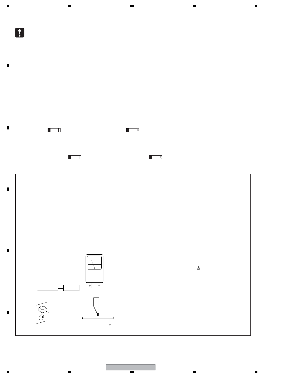
LEAKAGE CURRENT CHECK
Measure leakage current to a known earth ground
(water pipe, conduit, etc.) by connecting a leakage
current tester such as Simpson Model 229-2 or
D
equivalent between the earth ground and all exposed
metal parts of the appliance (input/output terminals,
screwheads, metal overlays, control shaft, etc.). Plug
the AC line cord of the appliance directly into a 120V
AC 60 Hz outlet and turn the AC power switch on. Any
current measured must not exceed 0.5 mA.
Leakage
current
E
Device
under
test
Also test with
plug reversed
(Using AC adapter
plug as required)
Test all
exposed metal
surfaces
AC Leakage Test
tester
Reading should
not be above
0.5 mA
Earth
ground
ANY MEASUREMENTS NOT WITHIN THE
LIMITS OUTLINED ABOVE ARE INDICATIVE
OF A POTENTIAL SHOCK HAZARD AND
MUST BE CORRECTED BEFORE RETURNING THE APPLIANCE TO THE CUSTOMER.
2. PRODUCT SAFETY NOTICE
Many electrical and mechanical parts in the appliance
have special safety related characteristics. These are
often not evident from visual inspection nor the
protection afforded by them necessarily can be obtained
by using replacement components rated for voltage,
wattage, etc. Replacement parts which have these
special safety characteristics are identified in this
Service Manual.
Electrical components having such features are
identified by marking with a
on the parts list in this Service Manual.
The use of a substitute replacement component which
does not have the same safety characteristics as the
PIONEER recommended replacement one, shown in the
parts list in this Service Manual, may create shock, fire,
or other hazards.
Product Safety is continuously under review and new
instructions are issued from time to time. For the latest
information, always consult the current PIONEER
Service Manual. A subscription to, or additional copies
of, PIONEER Service Manual may be obtained at a
nominal charge from PIONEER.
on the schematics and
F
2
1234
PD-D6-J
5678
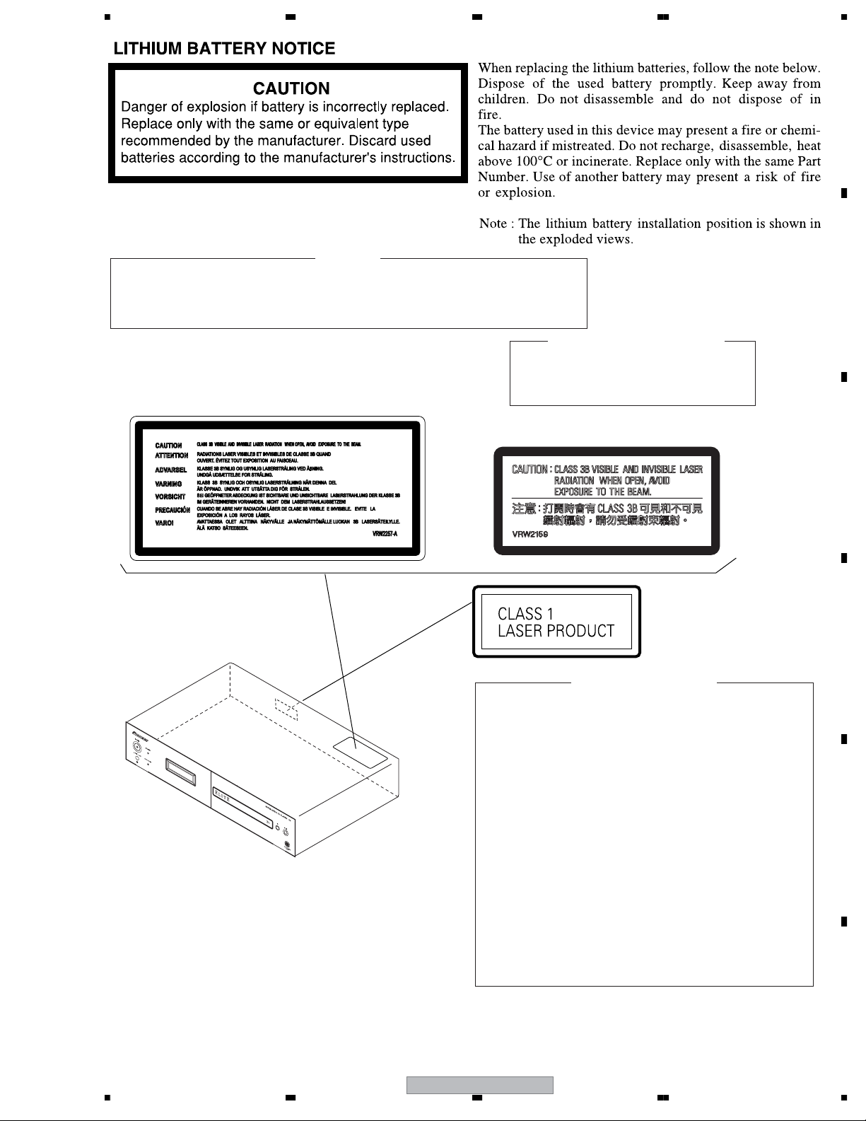
WARNING !
THE AEL (ACCESSIBLE EMISSION LEVEL) OF THE LASER POWER OUTPUT IS LESS THAN CLASS 1
BUT THE LASER COMPONENT IS CAPABLE OF EMITTING RADIATION EXCEEDING THE LIMIT FOR
CLASS 1.
A SPECIALLY INSTRUCTED PERSON SHOULD DO SERVICING OPERATION OF THE APPARATUS.
LASER DIODE CHARACTERISTICS
FOR CD : MAXIMUM OUTPUT POWER : 7 mW
(FOR DVD : MAXIMUM OUTPUT POWER : 5 mW
LABEL CHECK
KUXJ/CA, MYXJ5 types : VRW2257
A
B
WAVELENGTH : 780 nm
WAVELENGTH : 650 nm)
(Printed on the Rear Panel )
1. Laser Interlock Mechanism
• Loading switch (S101 on the LOAB Assy) is used for interlock
mechanism of the laser.
When this switch turned ON in SW2 (CLOSE) side (OPEN signal is
0V and CLOSE signal is 3.5V), a laser becomes the status which can
completely oscillation.
Furthermore, the laser completely oscillates in the disc judgment and
disc playback.
When player is power ON state and laser diode is not completely
oscillating, 780nm laser diode is always oscillating by half power.
• Laser diode is driving with Q307 (650nm LD) and Q308 (780nm LD)
on the DVDM Assy.
Therefore, when short-circuit between the emitter and collector of these
transistors or the base voltage is supplied for transistors turn on, the
laser oscillates. (failure mode)
• In the test mode ∗ , there is the mode that the laser oscillates except
for the disc judgment and playback. LD ON mode in the test mode
oscillates with the laser forcibly.
The interlock mechanism mentioned above becomes invalid in this
mode.
RLFPWXJ type : VRW2159
C
D
Additional Laser Caution
E
2. When the cover is open, close viewing through the objective lens with
the naked eye will cause exposure to the laser beam.
∗ : Refer to page 58.
PD-D6-J
56
F
3
7
8
1234
[Important Check Points for Good Servicing]
In this manual, procedures that must be performed during repairs are marked with the below symbol.
Please be sure to confirm and follow these procedures.
A
1. Product safety
Please conform to product regulations (such as safety and radiation regulations), and maintain a safe servicing environment by
following the safety instructions described in this manual.
1 Use specified parts for repair.
Use genuine parts. Be sure to use important parts for safety.
2 Do not perform modifications without proper instructions.
Please follow the specified safety methods when modification(addition/change of parts) is required due to interferences such as
radio/TV interference and foreign noise.
B
C
D
3 Make sure the soldering of repaired locations is properly performed.
When you solder while repairing, please be sure that there are no cold solder and other debris.
Soldering should be finished with the proper quantity. (Refer to the example)
4 Make sure the screws are tightly fastened.
Please be sure that all screws are fastened, and that there are no loose screws.
5 Make sure each connectors are correctly inserted.
Please be sure that all connectors are inserted, and that there are no imperfect insertion.
6 Make sure the wiring cables are set to their original state.
Please replace the wiring and cables to the original state after repairs.
In addition, be sure that there are no pinched wires, etc.
7 Make sure screws and soldering scraps do not remain inside the product.
Please check that neither solder debris nor screws remain inside the product.
8 There should be no semi-broken wires, scratches, melting, etc. on the coating of the power cord.
Damaged power cords may lead to fire accidents, so please be sure that there are no damages.
If you find a damaged power cord, please exchange it with a suitable one.
9 There should be no spark traces or similar marks on the power plug.
When spark traces or similar marks are found on the power supply plug, please check the connection and advise on secure
connections and suitable usage. Please exchange the power cord if necessary.
0 Safe environment should be secured during servicing.
When you perform repairs, please pay attention to static electricity, furniture, household articles, etc. in order to prevent injuries.
Please pay attention to your surroundings and repair safely.
2. Adjustments
To keep the original performance of the products, optimum adjustments and confirmation of characteristics within specification.
Adjustments should be performed in accordance with the procedures/instructions described in this manual.
3. Lubricants, Glues, and Replacement parts
Use grease and adhesives that are equal to the specified substance.
E
Make sure the proper amount is applied.
4. Cleaning
For parts that require cleaning, such as optical pickups, tape deck heads, lenses and mirrors used in projection monitors, proper
cleaning should be performed to restore their performances.
5. Shipping mode and Shipping screws
To protect products from damages or failures during transit, the shipping mode should be set or the shipping screws should be
installed before shipment. Please be sure to follow this method especially if it is specified in this manual.
F
4
1234
PD-D6-J

5678
CONTENTS
SAFETY INFORMATION......................................................................................................................................2
1. SPECIFICATIONS.............................................................................................................................................6
2. EXPLODED VIEWS AND PARTS LIST.............................................................................................................8
2.1 PACKING....................................................................................................................................................8
2.2 EXTERIOR SECTION ..............................................................................................................................10
2.3 FRONT PANEL SECTION ........................................................................................................................12
2.4 05 LOADER ASSY ...................................................................................................................................14
2.5 TRAVERSE MECHANISM ASSY-S ..........................................................................................................16
3. BLOCK DIAGRAM AND SCHEMATIC DIAGRAM ..........................................................................................18
3.1 BLOCK DIAGRAM....................................................................................................................................18
3.2 LOAB ASSY and OVERALL WIRING CONNECTION DIAGRAM............................................................20
3.3 DVDM ASSY (1/2) ....................................................................................................................................22
3.4 DVDM ASSY (2/2) ....................................................................................................................................24
3.5 AJKB ASSY (1/2)......................................................................................................................................26
3.6 AJKB ASSY (2/2)......................................................................................................................................28
3.7 LCD, PLED, MNSW, KEY, CONNECTOR, PRIMARY and TRANS ASSYS..............................................30
3.8 WAVEFORMS...........................................................................................................................................32
4. PCB CONNECTION DIAGRAM ......................................................................................................................35
4.1 LOAB ASSY..............................................................................................................................................35
4.2 DVDM ASSY.............................................................................................................................................36
4.3 AJKB ASSY ..............................................................................................................................................38
4.4 LCD ASSY................................................................................................................................................40
4.5 PLED, KEY and PRIMARY ASSYS..........................................................................................................42
4.6 CONNECTOR and MNSW ASSYS ..........................................................................................................44
4.7 PRIMARY ASSY.......................................................................................................................................46
5. PCB PARTS LIST............................................................................................................................................48
6. ADJUSTMENT ................................................................................................................................................56
6.1 ADJUSTMENT ITEMS AND LOCATION..................................................................................................56
6.2 JIGS AND MEASURING INSTRUMENTS ...............................................................................................56
6.3 NECESSARY ADJUSTMENT POINTS....................................................................................................57
6.4 TEST MODE .............................................................................................................................................58
6.5 MECHANISM ADJUSTMENT...................................................................................................................60
7. GENERAL INFORMATION .............................................................................................................................62
7.1 DIAGNOSIS..............................................................................................................................................62
7.1.1 TEST MODE.......................................................................................................................................62
7.1.2 METHOD FOR DIAGNOSING DEGRADATION OF THE LDS ON THE PICKUP ASSY...................63
7.1.3 TROUBLE SHOOTING.......................................................................................................................64
7.1.4 SEQUENCE AFTER POWER ON/OFF .............................................................................................68
7.1.5 DISASSEMBLY ..................................................................................................................................72
7.1.6 PANEL ADJUSTING...........................................................................................................................80
7.2 PARTS......................................................................................................................................................81
7.2.1 IC........................................................................................................................................................81
8. PANEL FACILITIES .........................................................................................................................................94
A
B
C
D
56
PD-D6-J
E
F
5
7
8
1234
1. SPECIFICATIONS
• General
System. . . . . . . . . . . . . . Super Audio CD player
A
B
Power requirements
Power requirements(MYXJ5)
. . . . . . . . . . . . . . .AC 220 V to 230V, 50 / 60 Hz
Power requirements(RLFPWXJ)
. . . AC 110 V, 60 Hz, 220 V to 240V, 50 / 60 Hz
Power consumption. . . . . . . . . . . . . . . . . . .22 W
Power consumption (standby) . . . . . . . . . 0.4 W
Weight . . . . . . . . . . . . . . . . . 4.5 kg (9 lb. 15 oz.)
Dimensions
. . . . . . 420 mm (W) x 100 mm (H) x 340 mm (D)
9
(16
/16 in. (W) x 3 15/16 in. (H) x 13 3/8 in. (D)
Operating temperature . . . . . . . . +5 to +35
Operating humidity . . . . . . . . . . . . . .5 % to 85 %
(KUXJ/CA)
. .AC 120 V, 60 Hz
(no condensation)
Disc / content format playback
compatibility
This player is compatible with a wide range of
audio disc types and media formats. Playable
discs will generally feature one of the following
logos on the disc and/or disc packaging. Note
however that some disc types, such as
recordable CDs, may be in an unplayable
formatósee the Disc compatibility table below
for further compatibility information.
Please also note that recordable discs cannot be
recorded using this player.
• Audio output (1 stereo pair)
Output level. . . . . . . . . . . . . During audio output
200 mVrms (1 kHz, -20 dB)
Number of channels . . . . . . . . . . . . . . . . . . . . . 2
Jacks . . . . . . . . . . . . . . . . . . . . . . . . . . . . . . RCA
Audio CD CD-R CD-RW
Super Audio CD
• Digital audio characteristics
Frequency response . . . 4 Hz to 50 kHz (SACD)
S/N ratio:
CD . . . . . . . . . . . . . . . . . . . . . . . . . . . . 118 dB
SACD. . . . . . . . . . . . . . . . . . . . . . . . . . 110 dB
C
Dynamic range:
CD . . . . . . . . . . . . . . . . . . . . . . . . . . . . . 99 dB
SACD. . . . . . . . . . . . . . . . . . . . . . . . . . 108 dB
Total harmonic distortion:
CD . . . . . . . . . . . . . . . . . . . . . . . . . . . 0.002 %
SACD. . . . . . . . . . . . . . . . . . . . . . . . . 0.003 %
Wow and flutter . . . . . . . . Limit of measurement
(±0.001 % W. PEAK) or lower
• Digital output
Coaxial digital output. . . . . . . . . . . . . . .RCA jack
Optical digital output. . . . . . . . Optical digital jack
4 Hz to 20 kHz (CD)
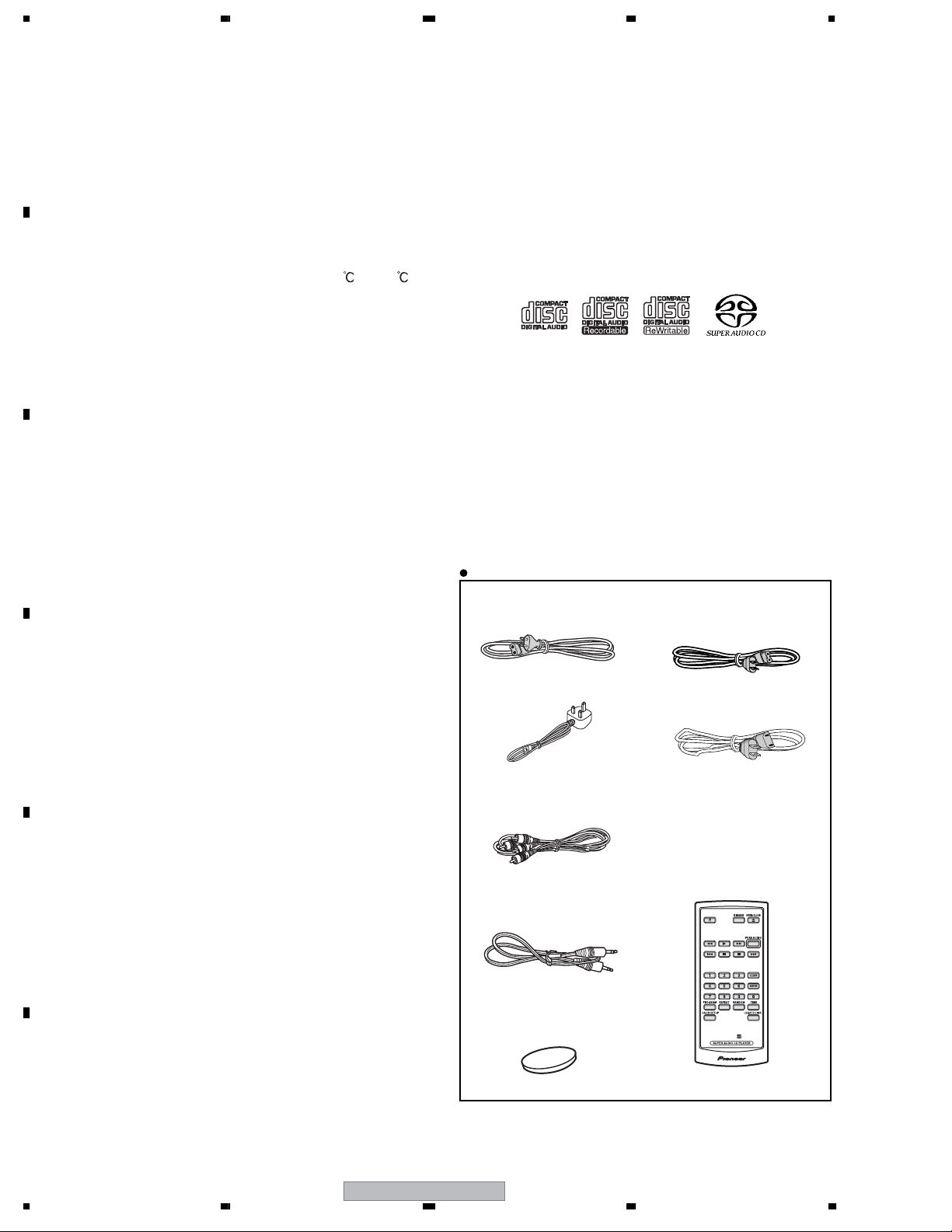
Accessories
• Power cable
(ADG7062 : MYXJ5)
(ADG7061 : KUXJ/CA)
• Accessories
Remote control . . . . . . . . . . . . . . . . . . . . . . . . . 1
D
Lithium battery (CR2025) . . . . . . . . . . . . . . . . . 1
RCA/phono stereo audio cable . . . . . . . . . . . . . 1
SR control cable . . . . . . . . . . . . . . . . . . . . . . . . 1
Power cable . . . . . . . . . . . . . . . . . . . . . . . . . . . 1
Operating Instructions
Warranty card
The specifications and design of this product are subject
to change without notice, due to improvement.
(ADG7104 : RLFPWXJ)
• RCA/phono stereo audio cable
(XDE3047)
(ADG7076 : RLFPWXJ)
• Remote Control
(PWW1175 : Except RLFPWXJ)
• SR control cable
E
F
6
1234
PD-D6-J
(XDE3063)
• Lithium Battery (CR2025)
>
(Attached inside the remote control)
(PWW1176 : RLFPWXJ type)

5678
A
B
C
D
E
56
PD-D6-J
F
7
7
8
1234
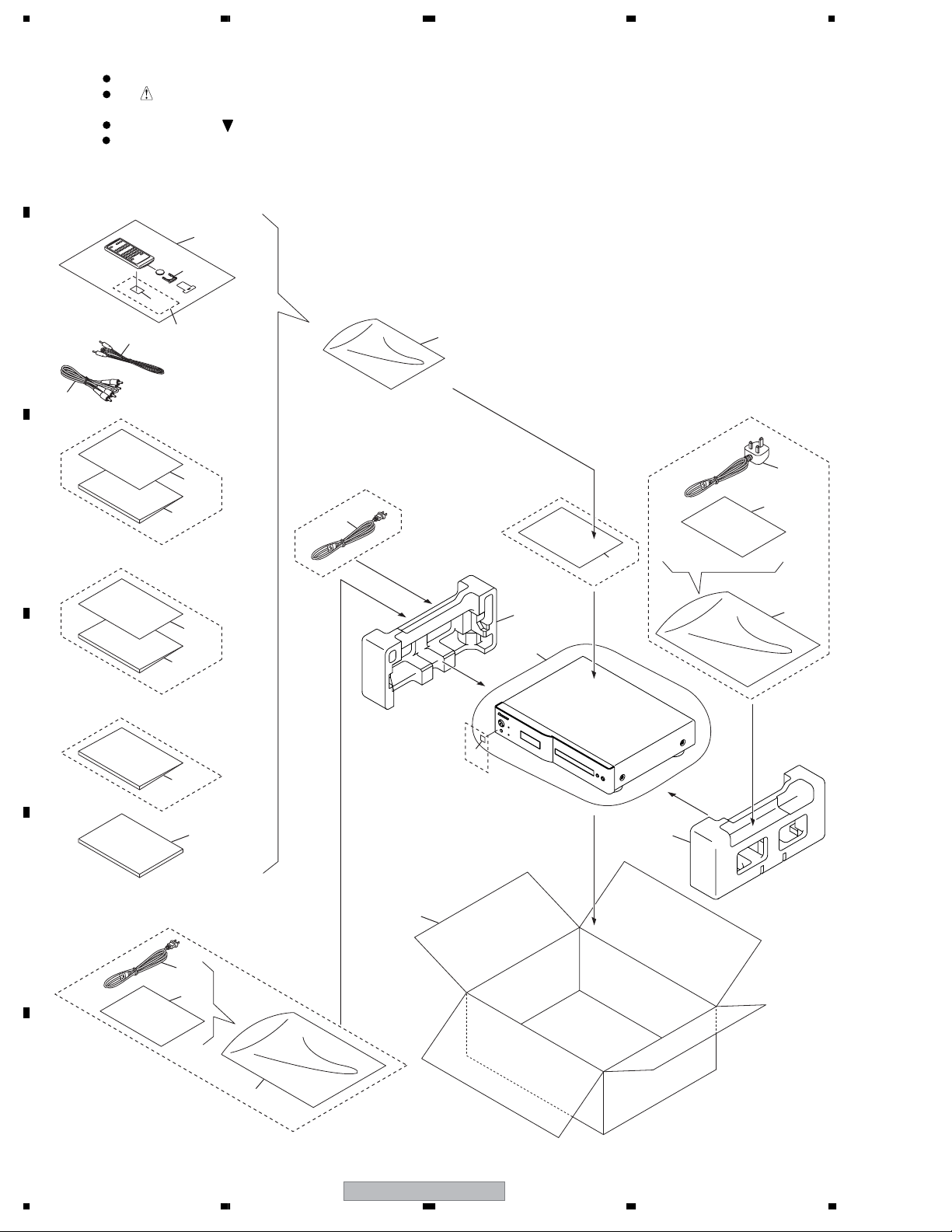
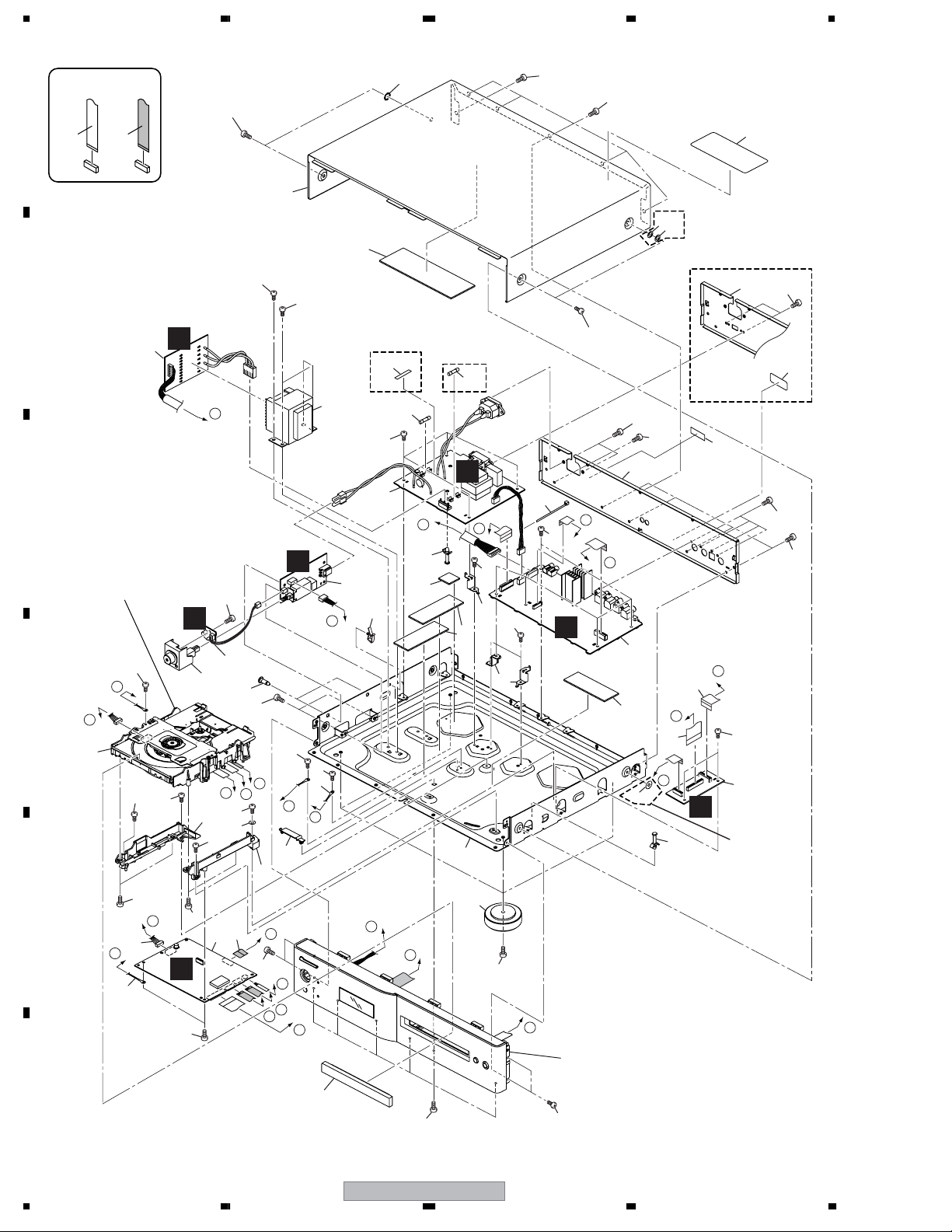
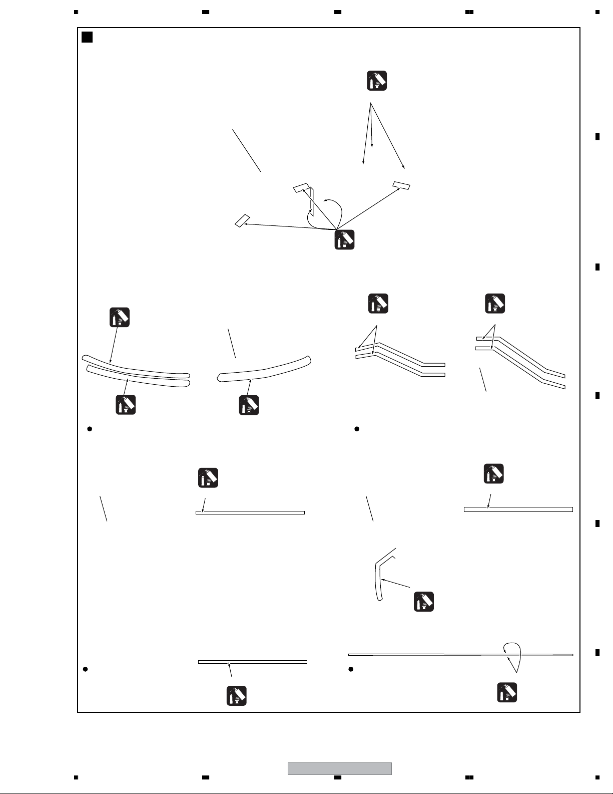
2. EXPLODED VIEWS AND PARTS LIST
NOTES:
Parts marked by "NSP" are generally unavailable because they are not in our Master Spare Parts List.
The mark found on some component parts indicates the importance of the safety factor of the part.
A
Therefore, when replacing, be sure to use parts of identical designation.
Screws adjacent to mark on product are used for disassembly.
For the applying amount of lubricants or glue, follow the instructions in this manual.
(In the case of no amount instructions, apply as you think it appropriate.)
2.1 PACKING
B
22
C
21
2
PD-D6-J/MYXJ5
23
Only
PD-D6-J/KUXJ/CA
Only
11
13
20
PD-D6-J/KUXJ/CA
PD-D6-J/MYXJ5
Only
3
6
PD-D6-S/RLFPWXJ
Only
PD-D6-S/RLFPWXJ
Only
4
9
PD-D6-J/MYXJ5
Only
16
12
5
14
D
E
PD-D6-S/RLFPWXJ
Only
15
18
3
8
PD-D6-J/KUXJ/CA
Only
19
1
10
7
17
PD-D6-S/RLFPWXJ
F
Only
8
1234
7
PD-D6-J
>
>
>
>
5678
(1) PACKING SECTION PARTS LIST
No. Description Part No.
Mark
NSP 1 Energy Star Label See Contrast table (2)
2 Label (WEEE) See Contrast table (2)
3AC Power Cord See Contrast table (2)
4AC Power Cord See Contrast table (2)
5Packing Sheet AHG7010
No. Description Part No.
Mark
(English)
14 Operating Instructions See Contrast table (2)
(English, French, German, Italian, Dutch, Spanish)
15 Operating Instructions See Contrast table (2)
(English, Chinese)
A
NSP 6 Polyethylene Bag AHG7117
NSP 7 Literature Bag See Contrast table (2)
8 Caution Card See Contrast table (2)
(SD SB)
9 Caution Card See Contrast table (2)
(SB)
10 Caution Card 220-240 See Contrast table (2)
NSP 11 Warranty Card See Contrast table (2)
(EL)
NSP 12 Warranty Card See Contrast table (2)
13 Operating Instructions See Contrast table (2)
16 PAD L PHA1353
17 PAD R PHA1354
NSP 18 Spacer PHC1097
19 Packing Case See Contrast table (2)
20 Remote Control Unit See Contrast table (2)
21 Battery Cover See Contrast table (2)
22 RCA/phono stereo audio cable XDE3047
23 SR control cable XDE3063
(2) CONTRAST TABLE
PD-D6-J/KUXJ/CA, PD-D6-J/MYXJ5 and PD-D6-S/RLFPWXJ are constructed the same except for the following :
Mark No. Symbol and Description
NSP 1 Energy Star Label AAX8022 Not used Not used
2 Label (WEEE) Not used ARW7322 Not used
3AC Power Cord ADG7061 ADG7062 ADG7076
4AC Power Cord Not used Not used ADG7104
NSP 7 Literature Bag Not used Not used AHG1180
PD-D6-J/
KUXJ/CA
PD-D6-J/
MYXJ5
PD-D6-S/
RLFPWXJ
B
C
8 Caution Card Not used Not used ARM7063
(SD SB)
9 Caution Card Not used Not used ARM7064
(SB)
10 Caution Card 220-240 Not used Not used PRM1078
NSP 11 Warranty Card ARY7007 Not used Not used
(EL)
NSP 12 Warranty Card Not used ARY7065 Not used
(EU)
13 Operating Instructions PRB1315 Not used Not used
(English)
14 Operating Instructions Not used PRD1071 Not used
(English, French, German, Italian, Dutch, Spanish)
15 Operating Instructions Not used Not used PRD1072
(English, Chinese)
19 Packing Case PHG2452 PHG2451 PHG2454
20 Remote Control Unit PWW1175 PWW1175 PWW1176
21 Battery Cover AZN8024 AZN8024 AZN8025
D
E
F
56
PD-D6-J
9
7
8
1234
2.2 EXTERIOR SECTION
A
NON-CONTACT
SIDE
B
C
Refer to
"2.4 05 LOADER ASSY".
M
D
E
H
17
L
13
CONTACT SIDE
J
6
E
47
43
44
H
12
31
40
23
44
B
44
43
39
40
43
41
45
27
37
E
40
F
C
7
20
50
B
Refer to
"2.3 FRONT PANEL SECTION".
PD-D6-S/RLFPWXJ
51
Only
52
PD-D6-S/RLFPWXJ
Only
40
10
B
33
F
11
G
H
22
35
27
43
43
46
4
PD-D6-S
/RLFPWXJ
Only
34
43
49
41
28
19
39
46
PD-D6-J/KUXJ/CA
PD-D6-S/RLFPWXJ
Only
36
D
14
15
46
PD-D6-S/
RLFPWXJ
Only
16
I
5
D
F
46
2
25
C
8
M
C
44
3
29
46
46
K
I
J
24
42
L
21
E
K
J
I
G
40
48
9
1
22
18
A
A
39
32
20
32
26
30
43
38
F
10
1234
43
PD-D6-J
42
>
>
>
>
5678
(1) EXTERIOR SECTION PARTS LIST
No. Description Part No.
Mark
1DVDM ASSY AWM8069
2 MNSW ASSY AWX8794
3 PLED ASSY AWX8795
4 CONNECTOR ASSY AWX8796
5 PRIMARY ASSY See Contrast table (2)
6 TRANS ASSY See Contrast table (2)
7 AJKB ASSY AWM8075
NSP 8 Cord With Plug ADH7022
9 17P FFC PDD1230
10 29P FFC PDD1231
11 15P FFC PDD1232
12 Connector ASSY PG05KK-E07
NSP 13 Cord With Plug DE005VF0
14 Power Transfomer See Contrast table (2)
15 Fuse 1 See Contrast table (2)
16 Fuse 2 See Contrast table (2)
NSP 17 05 LOADER ASSY VWT1230
18 Shield Cusion AEB7372
19 SR Sheet L PEB1319
20 SR Sheet S PEB1320
NSP 21 Flatcable Clamp AEC7376
22 PCB Spacer KGPS-12S AEC7517
23 Adapter05 L ANW7282
24 Adapter05 R ANW7283
25 Side Clamp DEC2007
NSP 26 Chassis PNA2602
No. Description Part No.
Mark
27 Rear Panel See Contrast table (2)
28 Bonnet See Contrast table (2)
29 PCB Holder PNW2029
30 Insulater See Contrast table (2)
31 Power Button ASSY See Contrast table (2)
NSP 32 PCB Angle 989 VNE2409
NSP 33 Label VRW1629
NSP 34 SISIR Label See Contrast table (2)
35 Caution Label See Contrast table (2)
36 Fuse Label See Contrast table (2)
NSP 37 Binder ZCA-BK1
38 Tray Panel See Contrast table (2)
39 Screw ABA1192
40 Screw ABA7017
41 Deco. Screw 4X10 See Contrast table (2)
42 Screw BBT30P080FNI
43 Screw BBZ30P080FCC
44 Screw BPZ30P080FTC
45 Screw CBZ30P080FCC
46 Screw IBZ30P060FCC
47 Screw VBA1094
48 Washer PEC1046
49 Washer WG40FCC
50 Spacer See Contrast table (2)
51 Washer See Contrast table (2)
52 Washer See Contrast table (2)
A
B
C
(2) CONTRAST TABLE
PD-D6-J/KUXJ/CA, PD-D6-J/MYXJ5 and PD-D6-S/RLFPWXJ are constructed the same except for the following :
Mark No. Symbol and Description
5 PRIMARY ASSY AWX8800 AWX8799 AWX8801
6 TRANS ASSY AWX8802 AWX8802 AWX8797
>
14 Power Transfomer PTT1369 PTT1368 PTT1370
>
15 Fuse 1 REK1058 REK1134 REK1023
16 Fuse 2 (T500 mA / 250 V) Not used Not used REK1134
27 Rear Panel PNA2606 PNA2605 PNA2607
28 Bonnet PNA2610 PNA2610 PNA2603
30 Insulater PNW2766 AMR7198 PNW2766
31 Power Button ASSY PXA1644 PXA1644 VXA2724
NSP 34 SISIR Label Not used Not used PRW1601
35 Caution Label VRW2257 VRW2257 VRW2159
36 Fuse Label XAX3161 Not used XAX3161
NSP 38 Tray Panel PNW3048 PNW3051 PNW3044
41 Deco. Screw 4X10 ABA7136 ABA7136 ABA7135
50 Spacer Not used Not used PEC1049
51
Washer
52 Washer Not used Not used WB40FTC
PD-D6-J/
KUXJ/CA
(1.25 A/ 250 V)
Not used Not used PEC1048
PD-D6-J/
MYXJ5
(T500 mA/ 250 V) (T1.25 A / 250 V)
PD-D6-S/
RLFPWXJ
D
E
F
56
PD-D6-J
11
7
8
1234
2.3 FRONT PANEL SECTION
A
17
14
Refer to
"2.2 EXTERIOR
SECTION. "
4
A
Refer to
"2.2 EXTERIOR
SECTION. "
3
G
2
12: 1/2
B
18
B
Refer to
"2.2 EXTERIOR
SECTION. "
1
16
C
15
6
5
D
11
8
9
7
17
C
18
D
10
13
E
F
12
1234
12: 2/2
PD-D6-J
NON-CONTACT
SIDE
CONTACT SIDE
5678
(1) FRONT PANEL SECTION PARTS LIST
No. Description Part No.
Mark
1 LCD ASSY AWX8790
2 KEY ASSY AWX8792
3 15P FFC PDD1229
4 17P FFC PDD1233
5D.Window PAM1866
No. Description Part No.
Mark
11 Lens See Contrast table (2)
NSP 12 Panel ASSY See Contrast table (2)
13 Tray Panel See Contrast table (2)
14 Panel Stay See Contrast table (2)
15 Pioneer Badge VAM1124
A
NSP 6 AL Panel L See Contrast table (2)
NSP 7 AL Panel R See Contrast table (2)
8 Himelon Sheet PEB1321
9 Earth Plate PNB1662
10 Earth Plate C PNB1664
NSP 16 LED Lens VNK5073
17 Screw BBZ30P080FCC
18 Screw BPZ30P080FTC
(2) CONTRAST TABLE
PD-D6-J/KUXJ/CA, PD-D6-J/MYXJ5 and PD-D6-S/RLFPWXJ are constructed the same except for the following :
Mark No. Symbol and Description
NSP 6 AL Panel L PAN1389 PAN1389 PAN1385
NSP 7 AL Panel R PAN1390 PAN1391 PAN1386
11 Lens PNW3047 PNW3047 AAK7586
NSP 12 Panel ASSY PXA1645 PXA1646 PXA1647
13 Tray Panel PNW3048 PNW3051 PNW3044
14 Panel Stay PNW3049 PNW3049 PNW3043
PD-D6-J/
KUXJ/CA
PD-D6-J/
MYXJ5
PD-D6-S/
RLFPWXJ
B
C
D
E
F
56
PD-D6-J
13
7
8
1234
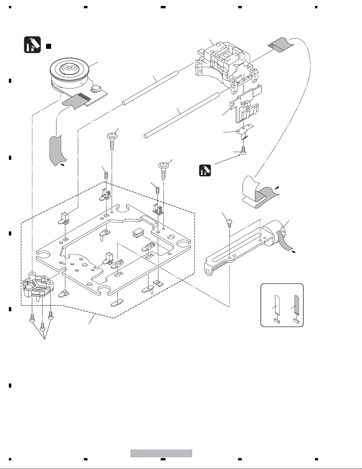
2.4 05 LOADER ASSY
A
B
C
Note :
Refer to
" Application of Lubricant".
Daifree
GEM1036
23
Lubricating Oil
GYA1001
13
22
Pickup leneses
Cleaning liquid
GEM1004
Cleaning paper
GED-008
8
12
16
8
2
Refer to
"2.5 Traverse Mechanism Assy-S".
6
8
To DVDM CN101 (Pickup)
To DVDM CN104 (Stepping Motor)
To DVDM CN102 (Spindle Motor)
8
18
17
3
A
24
19
20
22
15
14
D
05 LOADER ASSY PARTS LIST
Mark
No. Description Part No.
NSP 1 LOAB Assy VWG2346
2Traverse Mechanism Assy-S DXX2581
3 Loading Motor Assy VXX2912
E
4• • • • •
5• • • • •
6 Flexible Cable (24P) ADD7546
7 Connector Assy 2P VKP2253
8 Floating Rubber VEB1351
9 Belt VEB1358
10 Stabilizer VNE2253
22
To
DVDM CN103
9
21
22
7
A
10
11
1
A
Mark No. Description Part No.
16 Drive Gear VNL1923
17 SW Lever VNL1925
18 Clamper Plate 04 VNE2342
19 Bridge 04 VNE2343
20 Clamper 04 VNL1969
21 Screw JGZ17P028FTC
22 Screw VBA1094
23 Tray VNL1920
24 Clamp Magnet VMG1029
Lubricating Oil
GYA1001
11 Loading Base VNL1917
12 Float Base 04 VNL1968
F
13 Drive Cam VNL1919
14 Gear Pulley VNL1921
15 Loading Gear VNL1922
14
1234
PD-D6-J
5678
Application of Lubricant
Lubricating Oil
GYA1001
No. 11
Loading Base
No. 13
Drive Cam
Lubricating Oil
GYA1001
Around the shaft
Lubricating Oil
GYA1001
Lubricating Oil
GYA1001
Inner side of a ditch
A
B
Lubricating Oil
GYA1001
Inner side of a ditch
C
Lubricating Oil
GYA1001
Lubricating Oil
GYA1001
Front View Rear View
No. 23
Tray
Daifree
GEM1036
Concave of unevenness
No. 23
Tray
Top View Bottom View
Concave of unevenness
Daifree
GEM1036
Inner side of a ditch
Daifree
GEM1036
No. 13
Drive Cam
D
Daifree
GEM1036
Concave of unevenness
E
Side of the rib
Daifree
GEM1036
F
56
PD-D6-J
15
7
8
1234
2.5 TRAVERSE MECHANISM ASSY-S
Note :
A
B
C
Refer to
" Application of Lubricant".
Note : When part #2 is replaced,
2
11
To DVDM CN102
(Spindle Motor)
part #13 also need to be
replaced at the same time.
4
3
10
10
11
1
5
6
9
Silicone Adhesive
GEM1037
To
DVDM CN101
(Pickup Assy)
12
7
To
DVDM CN104
(Stepping Motor)
D
NON-CONTACT
8
Note : Spindle screw (DBA1252) of No.13 is the screw which applied special bond.
E
13
Therefore the adhesion becomes ineffective when takes it off once. Spindle screw is the part which cannot recycle.
When part #2 is replaced, part #13 also need to be replaced at the same time.
SIDE
CONTACT SIDE
F
16
1234
PD-D6-J

5678
TRAVERSE MECHANISM ASSY-S PARTS LIST
No. Description Part No.
Mark
1 05SD Pickup Assy-s OXX8019
2 Spindle Motor N200 DXM1197
NSP 3 Guide Shaft VK1 DLA1940
NSP 4 Sub Guide Shaft VK1 DLA1941
NSP 5 Joint VK1B DNK4272
NSP 6 Joint Spring VK1 DBK1235
7 Stepping Motor VK1 DXM1201
NSP 8 Mechanism Frame VK1 DNK4160
9 Precision Screw VK1 DBA1209
10 Skew Screw VK1 DBA1211
>
A
11 Skew Spring VK1 DBH1516
NSP 12 Stepping Screw DBA1205
13 Spindle Screw VK1(for Service) DBA1252
B
C
D
56
PD-D6-J
E
F
17
7
8
1234
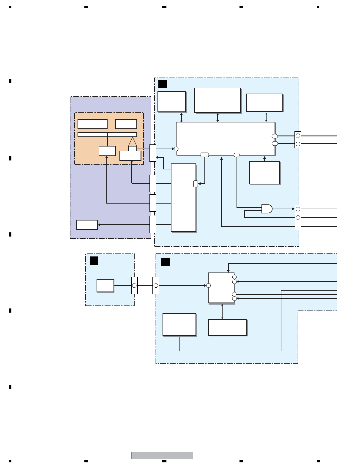
3. BLOCK DIAGRAM AND SCHEMATIC DIAGRAM
3.1 BLOCK DIAGRAM
A
DVDM ASSY
B
IC204
S-24CS04AFJ
EEPROM
4k
IC203
S29AL016D70TFI010-K
PGM FLASH
MEMORY
16M
IC202
K4S641632K-UC75
64M SDRAM
B
TRAVERSE
MOTOR
C
LOADING
MOTOR
G
D
S2301,S2302
05 PICK
SPDL
STEPPING
KEY ASSY
J2104A J2104
KEY
UP
PU
MOTOR
CN101
CN103
CN102
CN104
11
BD7995EFS
LCD ASSY
D
6
IC101
SERVO
DRIVER
41 42
9
10
IC201
MT1389EE/B2-L
MAIN DECODER
(CD,SACD)
IC2101
PDC148A
18
SYSTEM
CONTROL
CPU
225
90
7
41
5
ASPDIF
217
215
X202
ASS7075
(27MHz)
Clock OSC
IC205
TC7SH08FUS1
SPDIF RQ
CN953
CN901
DOUT
6
2
20
5
2401
GP1UM28XK0VF
IR
LCD Display
E
F
18
PD-D6-J
1234
5678
A
AJKB ASSY
C
L/R (DSD)
CN1501
6
2
CN2701
DOUT DOUT DOUT
10
SPDIF_RQ
25
L/R (PCM)
MCLK
CONNECTOR ASSY
H
IC1501
1
PD0274A
AQE
CN2503
24
6
J2102
6
5
6
5
2
LED2
2
CN2501
14
IC1601
TC74VHC157FTS1
PCM/DSD
SEL Lch
IC1602
TC74VHC157FTS1
PCM/DSD
SEL Rch
14
2
1
J13
2
1
7
755
11
I
IC1301
PCM1738EG-3
192k,24bit,
DAC Lch
IC1401
PCM1738EG-3
192k,24bit,
DAC Rch
CN2702
CN2703
5
CN2106
CN2105
SRIN
SROUT
SYSPOW SYSPOW
PRIMARY ASSY
IC1101 IC1102(1/2)
25
26
16
17
I/V
25
IC1201 IC1102(2/2)
26
16
17
3
2
1
16
J11
1
F
MNSW ASSY
CN2502
J2601
2
PLED
2
AC IN
J12
1
CN13
13
2
1
16
1
CN1851
CN1502
SRIN
SROUT
CN1503
J51
LPF
10.8V
8.3V
6.5V
5.8V
5V
3.3V
T51
POWER
SUPPLY
CN1801
J52
JA1101
L
JA1201
R
JA1702
OPTICAL OUT
JA1701
COAXIAL OUT
JA1751
SR-OUT
JA1752
SR-IN
B
C
D
E
PLED ASSY
E
SW11
Voltage Selector
PD-D6-S ONLY
PD-D6-J
56
TRANS ASSY
J
F
19
7
8
1234
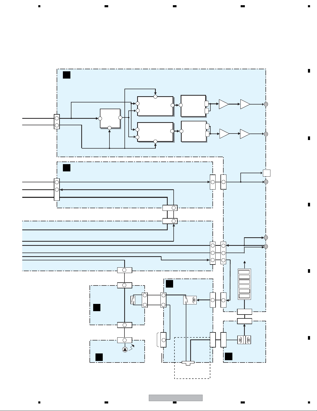
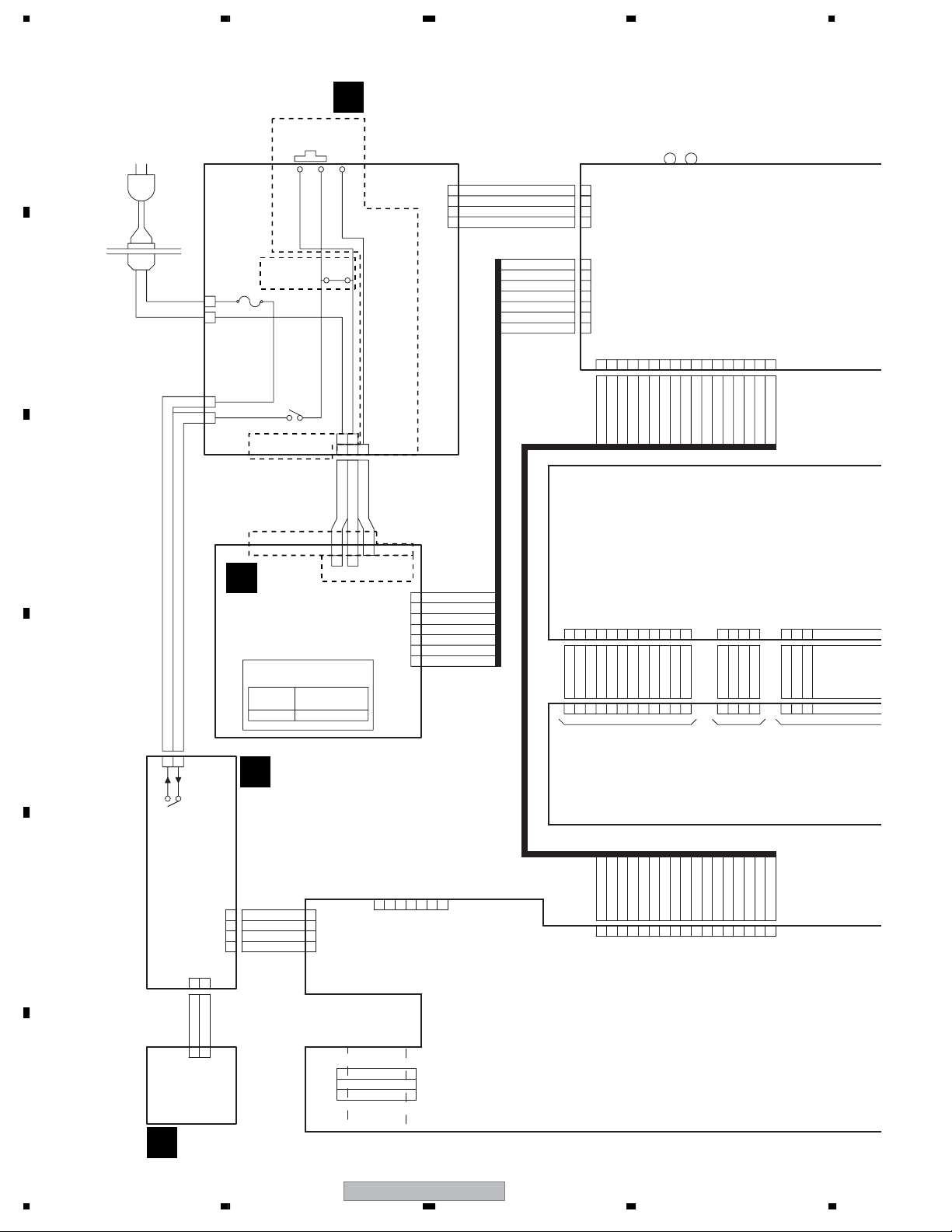
3.2 LOAB ASSY and OVERALL WIRING CONNECTION DIAGRAM
A
WY : ADG7062
KU : ADG7061
RD : ADG7076
ADG7104
AKX1033
HIGH
AC CORD
SW11
PD-D6-J
W124
AC INLET
PKP1014
B
PKP1015
J12
1
2
J13
1
2
ONLY
FU1
W129
RY11
PD-D6-J ONLY
B2P3-VH
PRIMARY ASSY
I
(PD-D6-J/KUXJ:AWX8800)
(PD-D6-J/MYXJ5:AWX8799)
LOW
(PD-D6-S/RLFPWXJ:AWX8801)
12
123
HOT(VH)
NEUTRAL
PD-D6-S
ONLY
B3P5-VH
CN13
VL
PF04PG-C07
J11
1
2
3
4
L=75mm
SYSPOW
AC
V+56ST
GNDU
AUDIO CT
AUDIO1
AUDIO2
DIGITAL1
DIGITAL2
MECHA1
MECHA2
B4B-PH-K-S
CN1503
1
2
3
4
CN1801
B7B-EH
7
6
5
4
3
2
1
21543
SRIN
SROUT
GNDD
GNDD
XDFDT
XDFCLK
SR-OUT
JA1751
RKN1004
876
XDFCS
XDFRST
SR-IN
JA1752
RKN1004
9
11
10
GNDD
V+56ST
XSYSMUTE
V+58U
141312
GNDU
GNDU
AC
CN1502
CKS3382
171615
SYSPOW
XDACRST
C
PD-D6-S ONLY
J
32
PD-D6-J ONLY
TRANS ASSY
(PD-D6-J:AWX8802)
(PD-D6-S:AWX8797)
Power
Transformer
D
1
2
VKN2024
S2301
(Mechanical
Power SW)
PD-D6-S
F
CN2501
PD-D6-J
WY : PTT1368
KU : PTT1369
RD : PTT1370
MNSW ASSY
(AWX8794)
J51
1
PKP1016
12
PKP1018
AUDIO CT
7
AUDIO1
J52
PKP1017
6
5
4
3
2
1
AUDIO2
DIGITAL1
DIGITAL2
MECHA1
MECHA2
PDD1233
L=300mm
P=1.25mm
FFC
P=1.0mm
FFC
12
V+5S
11
10
9876524
U+
V+
U-
2
1
3456789
SPINDLE MOTOR
AKN7031
CN102
W+
V-
RKN1045
CN103
1
3
INSIDE
HB
W-
W
U
V
10
11
P=1.0mm
FFC
12
STEPPING MOTOR
342
ST1+(A)
ST1-(A)
1
ST2+(B)
ST2-(B)
1
243
242322
FOCS DRV
FOCS RTN
TRKG RTN
214
3
21
TRKG DRV
WEN/DI
WCLK
WD0
VCC
VSS
RST
B4B-PH-K-S
CN2503
2
PLED
2
1
V+5U
1
1
2
3
4
L=75mm
L=120mm
E
CN2502
S2B-PH-K-S
PF02PG-C07
J2601
MSDCT
LED2
V+5U
GNDD
1
2
3
4
J2102
PF04PG-C12
IR
F
PLED ASSY
E
(AWX8795)
VOUT
V+5U
GNDD
W136
W137
W138
1
2
20
3
4
6
5
PD-D6-J
N.C.
7
CN2101
52492-0720
CN2105
9607S-17F
IROUT
SRIN
1
GNDD
254
3
GNDD
XDFDT
XDFCLK
XDFCS
XDFRST
876
XSYSMUTE
V+56ST
GNDD
9
11
10
GNDU
V+58U
GNDU
141312
AC
XDACRST
SYSPOW
171615
1234
Lch OUT
5678
A
Rch OUT
OPT-OUT
COAX-OUT
20
VSHF
191618
GNDD
JA1101
C
B
17
LD(650)PDLD(780)
PKB1041
JA1201
PKB1042
VKS1002
JA1702
(TOTX147L)
C 1/2, C 2/2
AJKB ASSY
(AWM8075)
134256789
MCLK(22M)
DATA0
LRCK
GNDD
GNDD
DATA1
GNDD
GNDD
134256789
B 1/2, B 2/2
DVDM ASSY
(AWM8069)
1514131211
GNDD
10
98765
10
987
VRCOM
VR780
VR650
RF
A
B
1418131211
PICKUP ASSY
MECHA ASSY
(AWM7967)
JA1701
GNDD
BCK
SW
171615
VKB1097
10
11
GNDD
10
11
C
D
1213141516
XDACCS1
XDACCK
XDACDT
1213141516
CN101
CKS5045
46512
3
VREF
VCC
E
XPCM/DSD
XDACCS2
GNDD
GNDD
F
2322212019
24
CN1501
VKN1248
17
L=120mm
PDD1230
P=1.0mm
17
CN953
CKS3885
L=220mm
ADD7546
P=0.5mm
CN601
S5B-PH-K-S
A
FFC
FFC
5
5
SW1
SW1
CN104
AKM1291
1
243
LOAD+
LOAD-
GNDD
SW2
342
1
LOAD+
LOAD-
V+3D
SW2
LOAB ASSY
(VWG2346)
CN901
PG05KK-E07
L=75mm
2
1
CN602
VKN1321
1
2
3
4
5
6
7
8
9
10
11
12
13
14
15
16
17
18
19
20
21
22
23
24
25
26
27
28
29
LOADING
MOTOR
ASSY
: VXX2912
CVBS
TROUT
TRIN
TRGAIN2726
SPDIF_RQ
TRKUP2524
DVDMUTE
VDET2322
GNDD
GNDD
ACK
MDATA 18
SDATA
SCLK 16
XREADY
XDVDRST 14
DVDPOWER
GNDD
GNDD
DOUT
GNDD109
GNDD 8
GNDM
GNDM
V+6R5V 5
V+6R5V
V+9D
V+9D32
V+12A 1
PDD1231
L=100mm
P=1.0mm
FFC
29
28
21
20
19
17
15
13
12
11
7
6
4
PDD1232
CN2701
VKN1205
PDD1229
P=1.25mm
L=125mm
FFC
H
L=285mm
P=1.0mm
FFC
GNDD
1
1415111213
GNDD
2
DOUT
345
8
9107563421
DVDMUTE
GNDM
GNDM
GNDD
GNDD
678
V+6R5V
V+6R5V
10
9
GNDD
111412
GNDD
V+9D
13
CONNECTOR ASSY
(AWX8796)
CN2704
B2P-SHF-1AA
101413
867119
MDATA
ACK
SCLK
12
XDVDRST
SDATA
XREADY
TRGAIN
TROUT
141312
TRIN
54321
SPDIFP_RQ
VDET
111510
GNDD
GNDD
987652431
CN1851
CKS3380
V+12A
V+9D
15
CN2702
CKS3380
2
1
CVBS
GNDD
CN2703
15
VKN1191
DVDPOWER
GNDD
CN2106
CKS3829
B
C
D
P=2.0mm
L=200mm
1
KEY1
2
VE+5
3
LCD ASSY
D
(AWX8790)
÷
When ordering service parts, be sure to refer to "EXPLODED VIEWS and PARTS LIST" or
J2104
GNDD
D20PYY0320E
"PCB PARTS LIST".
÷
The > mark found on some component parts indicates the importance of the safety factor
of the part. Therefore, when replacing, be sure to use parts of identical designation.
÷
: The power supply is shown with the marked box.
PD-D6-J
56
7
1
2
3
J2104A
KEY ASSY
G
(AWX8792)
E
F
21
8
1234
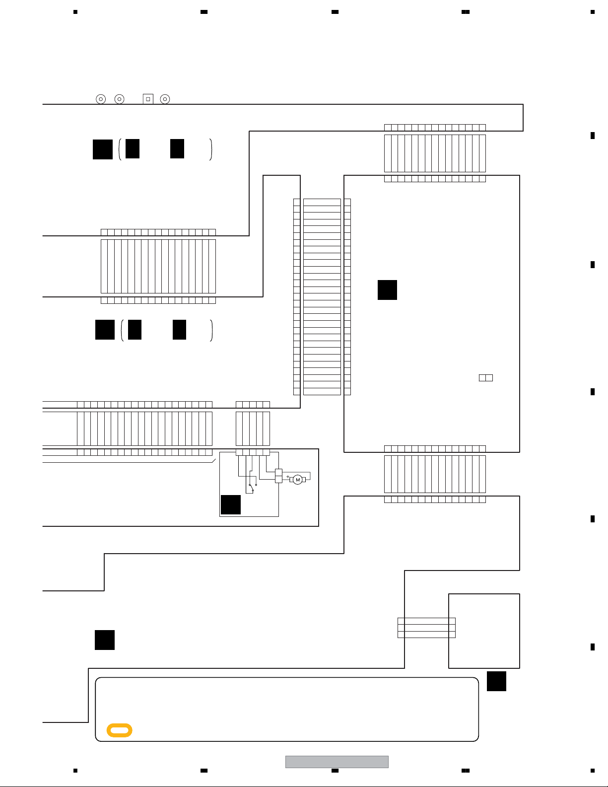
3.3 DVDM ASSY (1/2)
A
B 1/2
B
C
D
E
F
(AWM8069)
R301
V+5S0V20
GNDD GNDD
CN101
CKS5045
(side type)
VCH1260
C374
(47/35)
1
GNDD
VREF
VCC
SW
VR650
VRCOM
VR780
GNDD
LD(780)
LD(650)
GNDD
TRKG DRV
TRKG RTN
FOCS DRV
FOCS RTN
PD
VSHF
PICKUP ASSYSPINDLE MOTOR
CN102
INSIDE
HB
W-
W+
V+
U+
V+5S
CN103
ST2-(~B~)
ST2+(B)
ST1+(A)
ST1-(~A~)
STEPPING MOTOR
CN601
CN104
LOAD-
LOAD+
SW2
GNDD
SW1
A
(RF)
: RF SIGNAL ROUTE
(F)
: FOCUS SERVO LOOP LINE
(T)
: TRACKING SERVO LOOP LINE
(S)
: STEPPING SERVO LOOP LINE
(D)
: DIGITAL SIGNAL ROUTE
(AD)
: AUDIO DATA SIGNAL ROUTE
F
E
D
C
RF
B
A
AKN7031
(side type)
W
V
U
V-
U-
RKN1045
(side type)
AKM1291
(side type)
2
3
4
5
6
7
8
9
10
11
12
13
14
15
16
17
18
19
20
21
22
23
24
GNDD GNDD
1
2
3
4
5
6
7
8
9
10
11
12
1
2
3
4
1
2
3
4
5
GNDD
C373
GNDD
VCH1260
(47/35)
0.1
C372
0.1
C371
***
R375
***
R374
***
R373
***
R372
***
R371
R303
0
(T)
(T)
(F)
(F)
R302
0
4
LIMIT
V+5S
C140
1
(S)
(S)
(S)
(S)
LOAD-
LOAD+
TRIN
TROUT
IOA
F
E
D
C
IOA
RF
(RF)
B
A
MDI1
T+
T-
F+
F-
W
V
U
HW-
HW+
HV-
HV+
HU-
HU+
4.7
4.7
4.7
R132
R131
R133
ST2-
ST2+
ST1+
ST1-
TRIN
TROUT
Q305
UM5K1N
43
5
C102
1
V+6R5
4.7
4.7
4.7
C101
R134
100/16
R136
R135
***
C133
GNDM
2/2B 2/2B
R313
100K
2
R318
1
100K
HU-
HV+
HU+
***
***
C141
C142
44424338393740
41
HU-
HV+
HU+
VCC
IC101
FCO+
LDOP
LDON
FCO-
132
C153
C152
YBYBYB
0.01
(F)
(F)
LOAD+
LOAD-F-F+T+T-
V+5S
10K
R314
GNDD
HV-
HW-
HW+
***
C143
HB
HV-
HW-
HW+
SERVO DRIVER
BD7995EFS
AGND
AVM
TKO+
TKO68754
1
C103
C151
0.01
0.01
(T)
(T)
Q304
2SC4081(QR)
R315
10K
L309
***
L308
***
V
U
2200p
C145
C144
2200p
3335343631323029262724
V
U
SPVM1
SPGND1
TKIN
FCIN
LDIN
DVCC
1091112141516131821201917
SPGND2
SLVDD
1
R151
1.8
R152
W
C146
2200p
W
SPVM1
SLO1P
SLO1N
IOCE#
IOWR#
for ICE MODE
Q308
HN1A01F(YGR)
(1/2)
Q307
HN1A01F(YGR)
(1/2)
FG
CTL1
SPRNF
SLGND
SLO2N
SLO2P
1
C104
1
R153
(S)
1.8
R154
(S)
ST1-
ST1+
ALE
URD#
UWR#
CTL2
SLIN2
(S)
ST2+
TRGAIN
UP3_1
252823
SPIN
SLIN1
(S)
ST2-
INT0#
R326
6
R325
6
C161
1000p
VC
DGND
SLRNF2
SLRNF1
22
V+5M
2SA1576A(RS)
Q308
HN1A01F(YGR)
(2/2)
R321
4.7
2415
3
R322
4.7
2415
3
Q307
HN1A01F(YGR)
(2/2)
V1P4
0.1
C131
C121
1
(F)
(T)
Q101
Q102
DTC124EUA
4.7
4.7
GNDD
100/16
C132
GNDD
V+3D
C310
C309
R141
120k
R142
47/35
47/35
VCH1252-
22k
R284
10k
R285
***
V+3R3
***
R310
VCH1260
VCH1260
ENDM
DMSO
PWMOUT1
FMSO
TROPEN
FOSO
TRSO
C320
STBY
GNDD
LDO1
LDO2
FG
STBY
DMSO
FMSO
TROPEN
PWMOUT1
TRSO
FOSO
FG
TROUT
TRIN
STBY
ENDM
1
V+3D
1
C289
C296
1000p
GNDD
FLASH
IC203
S29AL016D70TFI010-K
PWR#
PCE#
D
A
B
C
RF
E
F
MDI1
LDO2
LDO1
V20
V1P4
C208
0.1
C209
(T)
(F)
B
R214
0
A2
A3
A4
A5
A6
A7
A8
A18
A19
SCL
SDA
A17
R282
***
47464845444241
A16
~BYTE~
A15
A14A8A12
231
A16
A15
V+1R8BEV+1R8
V+3RFV+3R3
R207
R200
0
0
1
C343
1
C346
1
C345
1
C344
1
C347
3.3v
C203
47/16
C204
C205
C206
47/16
56p
C210
C211
2200p
2200p
56p
C212
C
Q201
C218
*** 0.1
***
E
R215
***
R213
10K
R212
10K
R211
***
R210
***
1.8v
V+3R3 V+3D
R208
0
C290
10K
10K
81
VCC NC
7
WP
R219
R218
6
EEPROM
SCL
5
SDA
S-24CS04AFJ
A0
AD6
AD7
AD5
AD4
43
403839373634353332
D6
D7
D15
VSS
D4
D14
D12D5D13
AWY7119
A13
A10
A11
A9
A19
~WE~NC~RESET~NCNC
86745
12911101413151617
A14
A10
A13
A12A9A11
PWR#
A20
0.1
0.1
3.3v
IC204
VCC
C201
C202
220/4
220/4
(RF)
C207
0.1
C215
47/16
C213
0.1
C214
0.1
1.5K
R201
R202
22K
R204
22k
R205
180k
R206
220k
C216
C217
0.1
C219
1500p
R216
0
***
C221
0.1
2
NC
3
NC
4
GND
AD3
AD2
D2D3D9
D10
D11
A18
RY/~BY~
A17
A19
A18
DVDM ASSY
B 1/2
22
PD-D6-J
1234
0.1
C273
1
2
3
4
5
6
7
8
9
10
11
12
13
14
15
16
17
18
19
20
21
22
23
24
25
26
27
28
29
30
31
32
33
34
35
36
37
38
39
40
41
42
43
44
45
46
47
48
49
50
51
52
53
54
55
56
57
58
59
60
61
62
63
64
0.1
C220
AD0
AD1
20211918222423
15k
0.1
C272
R256
C271
256
253
254
255
252
AGND
DVDA
DVDB
DVDC
DVDD
DVDRFIP
DVDRFIN
MA
MB
MC
MD
SA
SB
SC
SD
CDFON
CDFOP
TNI
TPI
MIDI1
MIDI2
LDO2
LDO1
SVDD3
CSO/RFOP
RFLV/RFON
SGND
V2REFO
V2O
VREFO
FEO
TEO
TEZISILV
OP_OUT
3
OP_INN
OP_INP
DMO
FMO
TROPENPWM
PWMOUT1/V_ADIN9
TRO
FOO
USB_VSS
USBP
2
USBM
USB_VDD3
FG/V_ADIN8 (PU)
TDI/V_ADIN4 (JTAG)
TMS/V_ADIN5 (JTAG)
TCK/V_ADIN6 (JTAG)
TDO/V_ADIN7 (JTAG)
DVDD18
IOA2 (PU)
IOA3 (PU)
IOA4 (PU)
IOA5 (PU)
IOA6 (PU)
IOA7 (PU)
HIGHA0(PU)
IOA18 (PU)
IOA19 (PU)
DVSS
APLLCAP
APLLVSS
HIGHA6(PU)
666568677273706971
0
R217
0
R232
IOWR#
A16
PWR#
A14
A15
A1
PRD#
PCE#
28312930262527
A0
D0D8D1
VSS
~CE~
~OE~
A4A5A7A6A3A1A2
5678
A
RF
IOA
***
3.3v
1.8v
0.1
STBY
C270
C269
249
248
250
251
CEQP
CEQN
RFGND
CRTPLP
OSN:253
IREF:255
RFGC:254
AVDD3:256
65:APLLVSSVDD3
66:XIOWR
67:A16
68:HIGHA7(PU)
HIGHA4(PU)
HIGHA3(PU)
HIGHA5(PU)
DVDD3
0.1
C222
A11
A12
A13
V+3R3
C298
V1P4
100K
R255
C268
0.033
246
247
HRFZC
OSP:252
HIGHA2(PU)
747775
A10A9PRD#
X202
124
CONT
GND
ASS7075
(27MHz)
C262
1
242
241
ADCVSS
S_VREFP
0.1
C261
240
S_VCM
VDD
OUT
1
239
3
C260
238
LPFOP
ADCVDD3
R273
0
100
R271
10/16
C256
0.1
C259
C258
0.047
236
235
237
LPFIP
LPFIN
LPFON
(R203)
1
0.1
245
RFRPAC
L201
0
C299
GNDD
22p
C265
C267
C266
244
RFRPDC
1000p
C264
1000p
243
RFVDD3
S_VREFN
0.1
C263
0.1
MT1389EE/B2-L
HIGHA1(PU)
IOA20
XIOCS (PU)
AD0
AD1
DVDD3
XIOOE
IOCA1 (PU)
76807881798683828485879089
C223
0
R233
A1
A20
PCE#
DVSS (18)
AD4
AD3
AD2
0.1
IOCE#
AD0
AD1
AD4
AD2
AD3
0.047
AD5
R240
ACLK
ABCK
ASDAT2
ASDAT0
3333***
R246
R245
219
218
217
(PD) ASDATA2
(PD) ASDATA1
(PD) ASDATA0
333310
R244
R243
(AD)
216
215
(18) DVSS
ACLK
33
R242
10K
R249
214
ABCK
ALRCK
R241
C248
0.1
C240
10K
R247
213
212
DVDD3
(PD) ALRCK
DAC_XCS1
100
R270
C247
***
209
211
210
SPDATA
SPLRCK
SPBCK/ADATA5
XAMUTE
DAC_XCS0
1001k100
R268
R269
***
10k
R238
208
207
SPMCLK
HSYN/V_ADIN2
DAC_SO
DAC_SCK
100
R231
206
205
VSYN/V_ADIN1
YUV7/ASDATA5
C251
0.47
C255
234
PLLVDD3
***
C254
390p
R254
750K
0.1
C257
232
233
PLLVSS
IDACEXLP
GNDD
X201
***
R251
***
231
JITFN
230
JITFO
ASPDIF
ASDAT1
***
C252
33
***
DSD_Rch
R272
R248
***
R252 R253
(D)
0
R257
1.8v
0.1
XTALI
228
XTALO
227
RFVDD18
225
226
RFGND18
SPDIF
C241
223
224
MC_DATA
0.1
222
221
DVDD18
(3) DVSS
(PD) ASDATA4
220
(PD) ASDATA3
C253
229
5
IC201
IOA2/V_ADIN0
AD5
ALE (PU)
AD6
AD7
A17
XUWR (PU)
DVSS (3)
IOA0 (PU)
UP1_3 (PU)
UP1_2 (PU)
DVDD18
XURD (PU)
UP1_4 (PU)
UP1_7 (PU)
UP1_5 (PU)
UP1_6 (PU)
UP3_4 (PU)
UP3_5 (PU)
UP3_1 (PU)
UP3_0 (PU)
DVDD3IRICE (PD)
XINT0 (PU)
XPRST (PU)
DVSS (18)
DQS0
DQM0
101
100
103
102
106
105
107
104
88
929391
9499959896
97
0.1
C224
R235
URD#
4.7k
33333333333333
R237
R221
R258
R234
3.3v
1.8v 1.8v
33
R224
AD6
ALE
AD7
A17A0UWR#
108
0.1
220p
C225
C227
TXD
RXD
R261
R260
R259
SCL
SDA
UP3_1
V+3DR
XREADY
GNDD
R909
6.8k
R908
SCLK
ACK
MDATA
SDATA
324
1
LIMIT
3.3k
CN204
***
DOWNLOAD
RD7
112
109
111
110
116
115
113
114
***
***
***
0.01
C226
R220
R236
R239
33
R223
DQM0
DQ7
INT0#
XDVDRST
DAC
control
R_CR
R230
204
203
DVDD3
DACVDDC:189
RD6
118
117
DQ6
DQ5
B_CB
0.1
0.1
C246
C239
201
202
YUV5/B
YUV6/R
DACVSSA
YUV0/CIN:192
FS:191
VREF:190
DVSS (3)
RD4
RD5
120
119
0.1
C228
DQ4
(AD)
G_CY
CVBS
200
198
199
YUV4/G
DACVDDA
YUV3/CVBS
(INPUTPU) RD16
(INPUTPU) RD17
(INPUTPU) RD18
(INPUTPU) RD19
(INPUTPU) RD20
(INPUTPU) RD21
(INPUT PU) DQM2
(INPUTPU) DQM3
(PU)RD3/ASDATA5
RVREFN_ADIN3
126:RD15
RD3
DVDD18
RD2
121
122
123
DQ3
DQ2
S_C
0.1
C245
197
196
195
YUV2/C
DACVSSB
DACVDDB
(INPUT) RD24
(3) DVSS
DVDD18
(PU) RD30
(18) DVSS
(3) DVSS
DVDD18
(3) DVSS
(18) DVSS
(3)DVSS
127:DVDD3
128:RD14
RD0
RD1
125
124
126
C230
1000p
DQ0
DQ1
DQ15
S_Y
DVDD3
RD22
RD23
RD25
RD26
RD27
RD28
RD29
DVDD3
RA11
RCLK
DVDD3
RCLKB
RA10
XRCS
DVDD3
XRAS
XCAS
XRWE
DQM1
DQS1
RD10
RD11
RD12
RD13
194
YUV1/Y
RA4
RA5
RA6
RA7
RA8
RA9
CKE
RA3
RA2
RA1
RA0
BA1
BA0
RD8
RD9
127
193
DACVSSC
128
DQ14
GNDD
192
191
190
189
188
187
186
185
184
183
182
181
180
179
178
177
176
175
174
173
172
171
170
169
168
167
166
165
164
163
162
161
160
159
158
157
156
155
154
153
152
151
150
149
148
147
146
145
144
143
142
141
140
139
138
137
136
135
134
133
132
131
130
129
C250
3.3v
3.3v
1.8v
3.3v
0.01
C237
220/4
C242
***
C243
1
0.1
C244
C236
0.1
R267 R262
0 ***
C235
0.1
R266
33
C234
0.1
3.3v
C233
0.1
C232
0.1
C231
0.1
GNDD
(D)
to AUDIO PART
(Page 2/2)
to VIDEO PART
e 2
g
a
(P
/2
AUDIO
B
2/2
VIDEO
)
V+3R3V+3V
R209
0
***
560F
R280
R279
R265
***
R264
***
R263
***
VSEL2
VSEL1
LETTER
SQUEEZE
I/XP
MA4
MA5
R229
R228
R227
R226
R225
33*4
RAB4C330J
MA6
MA7
MA8
MA9
MA11
SDCKE
33
SDCLK
***
MA3
MA2
MA1
MA0
MA10
33
DBA1
33
DBA0
DCS#
DRAS#
DCAS#
DWE#
DQM1
1.8v
DQ8
DQ9
DQ10
DQ11
DQ12
DQ13
MA4
MA5
MA6
MA7
MA8
MA9
MA11
DQM1
DQ8
DQ9
DQ10
DQ11
DQ12
DQ13
DQ14
DQ15
C281
220/4
C285
V+3D V+3DR
R281
C284
0.1
0.1
0
1
C282
VSS
A4
A5
A6
A7
A8
A10/AP
A9
A11
NC
CKE
CLK
UDQM
NC
LDQM
VSS
DQ8
VCCQ
VSSQ
64M SD-RAM
IC202
DQ9
K4S641632K-UC75
DQ10
VCCQ
VSSQ
DQ11
DQ12
VSSQ
VCCQ
DQ13
DQ14
VCCQ
VSSQ
DQ15
VSS VCC
VCC
BA1
BA0
RAS
CAS
WE
VCC
DQ7
DQ6
DQ5
DQ4
DQ3
DQ2
DQ1
DQ0
28
29
30
31
32
33
34
35
36
37
38
39
40
41
42
43
44
45
46
47
48
49
50
51
52
53
54 1
STBY
V+5V
R601
R602
C283
0.1
27
A3
A2
A1
A0
CS
MA3
26
MA2
25
MA1
24
MA0
23
MA10
22
DBA1
21
DBA0
20
DCS#
19
DRAS#
18
DCAS#
17
DWE#
16
DQM0
15
14
DQ0
13
C288
0.1
12
DQ1
11
DQ2
10
9
DQ3
8
DQ4
7
C287
0.1
6
DQ5
5
DQ6
4
3
DQ7
2
C286
0.1
GNDD
***
***
*** ***
R604 R603
GNDD
B
C
D
E
Chip Size
DIODE
1SS355
RESISTOR
:2125 Size
RS1/10S***J
:1608 Size
TRKUP
2/2B
SYS
CAPACITOR
(F):RS1/16S****F
OTHERS:RS1/16S***J
:2125 Size
CKSQ**~
:1608 Size
CH:CCSRCH~
OTHERS:CKSRYB~
A8A7A6A5A4A2A3
56
PD-D6-J
F
B 1/2
23
7
8
1234
3.4 DVDM ASSY (2/2)
DVDM ASSY
CN951
VKN1417
10 569783214
13 1112
B 2/2
1/2B
from PAGE 1/2
STBY
GNDD
***
R500
(AWM8069)
ASPDIF
DAC 2ch
C501
C506
10/16
STBY
0.1
C592
R501
STBY
R594
PCM OUT
R595
V+3R3
C591
***
GNDD
R591
0
R505
R504
R503
0.1
C507
0
***
C502
ABCK
ACLK0 ABCK0
ALRCK
ASDAT0
ASDAT1
ASDAT2
ACLK
ABCK1
ABCK0
ASDAT0
ALRCK
V+3R3
R502
0
***
C505
GNDA
1
C500
V+5V
0
R590
0
0
1
TC7SHU04FU
5
2
3
AUDIO
(FL,FR)
100
100
100
GNDD
C503
100/16
(D)
STBY
IC591
4
DAC
0.1
C504
IC501
PCM1753DBQ
1
PCMBCK PCMMCK
2
PCMDATA
3
PCMLRCK
4
GNDD
5
VDD ZEROL/NA
6
VCC
ZEROR/ZEROA
7
VOUTL
8
VOUTR
ABCK1
R592
10
VOLTAGE DETECT
ACLK0
V+6R5 V+5V
D862 D861
D852
V+5V
V+12 V+12
R851 R881
47K
10K
Q851
10K
R853 R852
GNDD
V+12
GNDD
R823
R824
15K
10K
2SA1576A(RS)
47K
R822
D851
Q821
R821
2SA1576A(RS)
10k
R882
R883
GNDD
VPR+8
47K
10K
***
D821
Q881
D881
Q801
DTC124EUA
V+3R3
2SA1576A(RS)
R801
GNDD
470
D801
UDZS4.7B
NORMAL : 3.3V
ABNORMAL : 0.5VDD
0.85VDD
0.1
C801
VDET
(D)
V+5V
1K
R520
Q506
Q504
CH
CH
1000p 1000p
V+5V
R518
DTC114YUA
GNDD
DTC114YUA
1K
E
B
GNDA
FL
FR
1/2
SYS
GNDD
Q505
2SA1576A(RS)
C
R519
10K
2SD2114K(VW)
R515
2.2K
R516
2.2K
2SD2114K(VW)
B
STBY
Q501
Q502
R517
1K
XAMUTE
ACLK0
22
16
R506
100
15
R507
CS
14
R508
SCK
13
R509
SI
12
11
10
VCOM
9
GNDA
C508
DAC_XCS0
DAC_SCK
100
DAC_SO
100
Q503
DTC114YUA
0.1
C511
C509
10/16
10/16
C512
10/16
R512 R511
R513
470
22K 22K
C514 C513
R514
470
DVDMUTE
to PAGE 1/2
(D)
A
AUDIO
GNDD
MCLK
GNDD
LRCLK
GNDD
DATA0
GNDD
DATA1
GNDD
B
DATA2
GNDD
BCLK
GNDD
C
D
E
F
24
CN953
CKS3885
1
GNDD
2
MCLK
3
GNDD
4
LRCLK
5
GNDD
6
DATA0
7
GNDD
8
DATA1
9
GNDD
10
BCLK
11
GNDD
12
SO
13
SCL
14
XCS0
15
XCS1
16
GNDD
17
DATA2
GNDD
CN1501
1/2
C
B 2/2
(L931)
(L936)
R936
(L937)
R937
(L938)
R938
(L939)
R939
R931
CTF1384
R932
R933
R934
R935
R940
0
0
0
0
0
CTF1389
CTF1389
CTF1389
CTF1389
(AD)
ACLK0
ALRCK
ASDAT0
ASDAT1
ABCK1
DAC_SO
DAC_SCK
DAC_XCS0
DAC_XCS1
ASDAT2
DSD_Rch
external DAC control
Chip Size
DIODE
RESISTOR
CAPACITOR
1SS355
Size
RS1/10S***J
:1608 Size
(F):RS1/16S****F
OTHERS:RS1/16S***J
:2125Size
CKSQ**~
:1608 Size
CH:CCSRCH~
OTHERS:CKSRYB~
***:parts not mounted
VIDEO
B
from PAGE 1/2
1/2
PD-D6-J
1234
5678
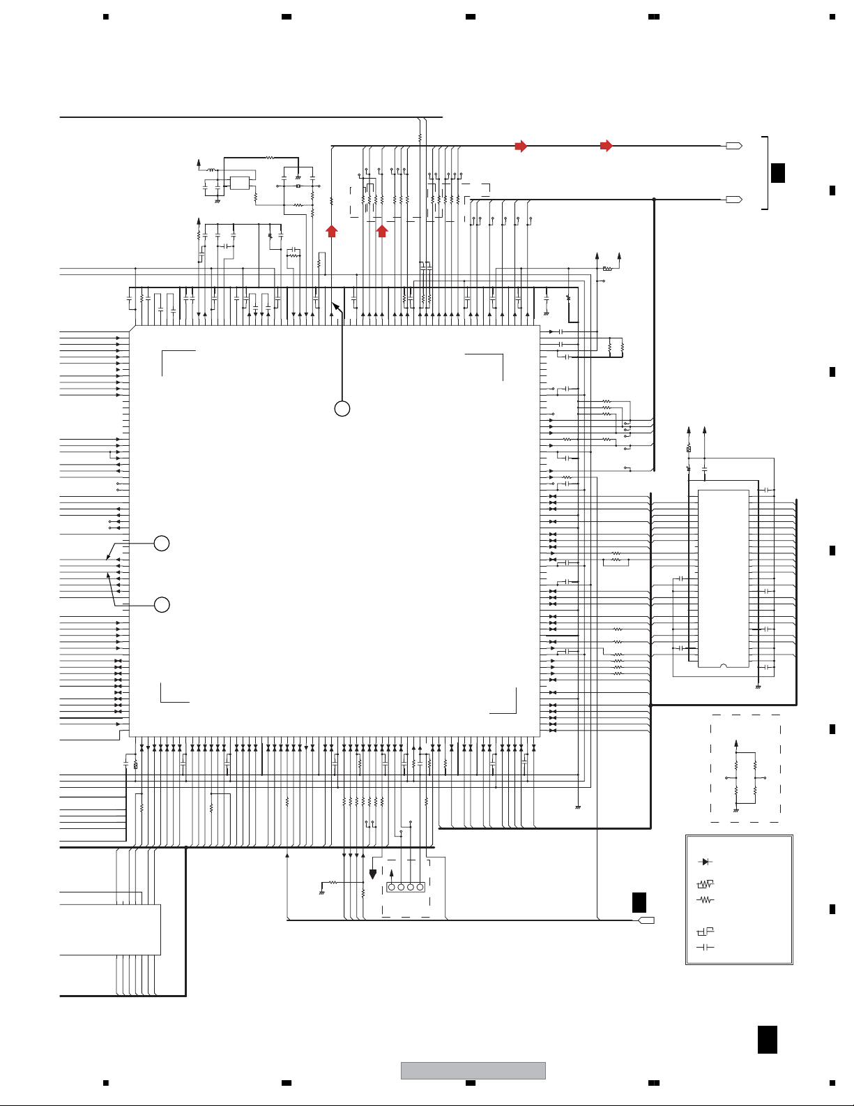
V+1R8
IC711
MM1661JH
18
C714
Vo
2
NC
3
GND NC
***
R714
45
***
C713
Cn
2.2
******
R713R712
C712
470P
GNDD
Vin
NC
Cont
5.0V
V+3D
C249
0.1
GNDD
5
2
R250
4
0
1
3
IC205
TC7SH08FUS1GNDD
S_C
******
GNDD
CVBS
*** 75
R432 R412 R411R431
GNDD
S_Y
*** ***
GNDD
G_CY
*** ***
GNDD
B_CB
*** ***
R435 R415 R434 R414 R433 R413
GNDD
R_CR
******
R436 R416
GNDD
(D)
: DIGITAL SIGNAL ROUTE
(AD)
: AUDIO DATA SIGNAL ROUTE
V+12
Q732
RSQ035P03
65
***
C701
1
534
10
DCH1165
C763
R406
75
C402
C452
C702
4
GNDD
L731
DTL1099
22
10
C733
C734
100/16
DCH1165
R765
***
***
IC761
***
R764
R763
4
***
***
R762
V+5V
C401
100/16
0.1
SQUEEZE
LETTER
I/XP
GNDD
V+5V
C451
100/16
0.1
GNDD
L732
ATH7011
22
VIN
R751
1
6.5V
C736
21
3
Q731
***
2
D732
RSX201L-30
5
10
R732
22
R733
4
D733
C735
0.1
V+6R5
0
C761
100/16
V+3R3
R711
***
7
6
C711
V+5S
L751
CTF1395
C754
10
1
R738
***
100/16
R737
C738
C740
C739
DCH1165
R736
0
R739
V+5MV+5V
0
R750
***
C753
2.2
C752
GNDD
C737
120P
15K(F)
R735
2.7K
27K(F)
18K(F)
R734
GNDD
7.8V
IC751
MM1565AF
1
Vo Vin
2
NC
3
GND
4
Cn
470P
DC-DC CONVERTER
IC731
R1224N102H
1
CE
2
GND
3
VOUT EXT
47k
D731
R740
0
STBY
D751
1SR154-400
75
Sub
6
C751
Cont
5
(D)
VSEL1 RGB V
C454
100/16
C455
C403
R404
C453
0.1
***
*2
***
1
2
3
4
5
6
7
8
9
10
11
12
13
14
*2
R405
EXTRA VIDEO OUT
1
2
3
4
5
6
7
8
VSEL2 V+RGB S
IC401
MM1623BF
Vcc1
C in
DC out
MUTE1
V in
YC MIX
Y in
GND1
BIAS
I/P
CY out
CY in
CLP
Cb out
Cb in
MUTE2
Cr in
IC451
MM1566AJ
Vcc1
R in
MODE2
MUTE1
G in
MODE1
B in GND2
BIAS
GND1
C out
GND2
GND2
GND2
Cr out
GND2
R out
G out
VSAG
YSAG
Vcc2
V out
Y out
Vcc2
B out
28
27
26
25
S1
24
S2
23
22
21
20
19
18
17
16
15
16
15
14
13
12
11
10
9
DTC114YUA
VSEL1
Q401
*2
R404
except
PROGRESSIVE
STBY
CN904
C411
C412
C413
C414
C415
C416
V+5V
R401
GNDD
C464
C465
C466
PROGRESSIVE
1K
1KR405
STBY
***
1
432
0.1
1
1
C404
100/16
C405
0.1
1
0.1
0.1
10K
0.1
0.1
0.1
2SA1576A(RS)
1
GNDD
C732
DCH1165
0
1
2
3
GNDM
I/XP
SQUEEZE
VSEL2
VSEL1
Q701
R702
VDVD+12
A
VPR+8
47K
R701
10K
Q702
DTC124EUA
R731
***
10
***
C731
R761
***
***
C762
Q481
DTC114YUA
C406
0.1
V+5V
GNDD
R481
R402
(D)
R901
0
R902
L901
CTF1334
R921
R922
R923
R924
R403
R421
R422
R423
R424
R425
R426
R474
R475
R476
R521
R522
DAC 2ch
R903
3.3k
R905
3.3k
R907
470
R918
***
R910
220
R911
220
R912
R913
R914
1/2B
0
0
0
0
0
0
0
0
0
0
0
0
0
0
0
0
C1001
GNDA GNDAGNDD
0
0
0
10k
R915
R920
TRGAIN
***
XDVDRST
XREADY
SCLK
SDATA
MDATA
ACK
VDET
DVDMUTE
TRKUP
PROGRESSIVE
1K
10K
FL
FR
GNDM
TRIN
TROUT
C421
***
C422
***
C423
***
C424
***
C425
***
C426
***
C474
***
C475
***
C476
***
C1002
R904
6.8k
R906
6.8k
R916
R919
R917
C1003
***
22K
***
22k
6.8k
3.3k
GNDD
CN901
***
CN952
CN902
GNDD
CN905
VKN1321
29
28
27
26
25
24
23
22
21
20
19
18
17
16
15
14
13
12
11
10
9
8
7
6
5
4
3
2
1
1
2
AKM1288
STBY
VKN1319
1
2
3
4
5
6
7
8
9
10
11
12
13
14
15
16
17
18
19
20
21
22
23
24
25
26
27
***
1
2
3
4
5
VDVD+12
VPR+8
VPR+8
6R5V
6R5V
GNDM
GNDM
GNDD
GNDD
DOUT
GNDD
GNDD
DVD
POWER
XDVDRST
XREADY
SCLK
SDATA
MDATA
ACK
GNDD
GNDD
VDET
DVDMUTE
TRKUP
SPDIF_RQ
TRGAIN
TRIN
TROUT
CVBS
P/XI
SQUEEZE
VSEL2
VSEL1
ASPECT
SC
GNDD
V
GNDD
SY
GNDD
CY/G
GNDD
Cb/B
GNDD
Cr/R
GNDD
R
GNDD
G
GNDD
B
GNDD
GNDA
FL
GNDA
FR
GNDA
FR
GNDA
FL
GNDA
B
CN2701
H
C
D
E
STBY
(C1011)
R1001
CKSQYB104K16
R1002
***
R1003
GNDD2
***
GNDD
F
56
PD-D6-J
B 2/2
25
7
8
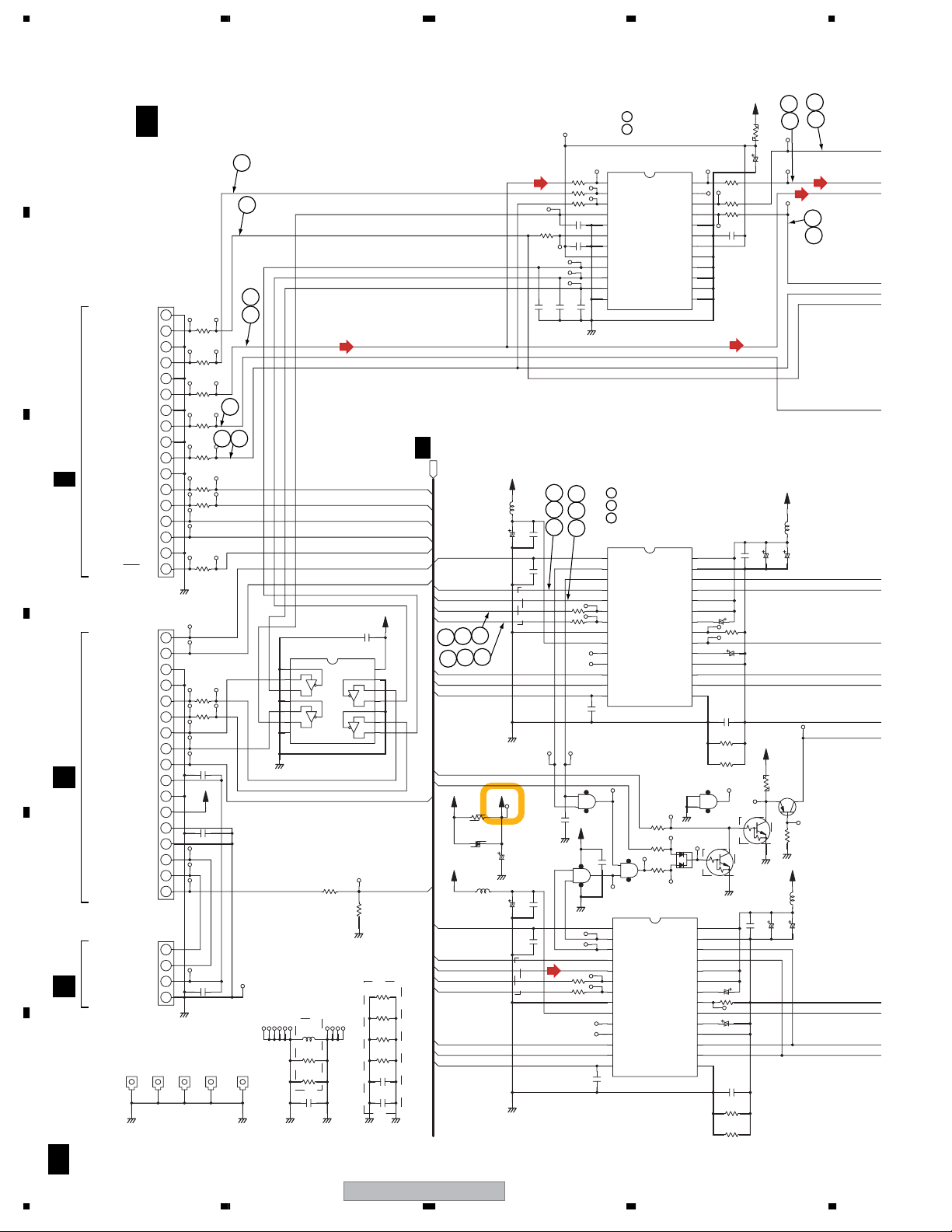
1234
3.5 AJKB ASSY (1/2)
A
C 1/2
CN1501
B
CN953
2/2
B
C
D
CN2105
D
E
J11
I
F
VKN1248-
GNDD
MCLK(22M)
GNDD
LRCK
GNDD
DATA0
GNDD
DATA1
GNDD
BCK
GNDD
XDACDT
XDACCK
XDACCS1
XDACCS2
GNDD
PCM/DSD
CN1502
CKS3382-
SROUT
SRIN
GNDD
GNDD
XDFDT
XDFCLK
XDFCS
XDFRST
XSYSMUTE
V+56ST
GNDD
V+58U
GNDU
GNDU
AC
SYSPOW
XDACRST
CN1503
B4B-PH-K-S
SYSPOW
AC
V+56ST
GNDU
KN1902 KN1903KN1901 KN1905 KN1904
GNDD GNDS
AJKB ASSY
(AWM8075)
1
R1515
2
68
3
R1507
4
68
5
R1508
6
68
7
R1509
8
68
9
R1510
10
68
11
R1511
12
10
R1512
13
10
14
15
16
R1513
17
10
GNDD
1
2
3
4
R1516
5
22
R1517
6
22
7
8
9
C1511
10
V+58U
11
12
C1510
13
*
14
15
16
17
1
2
3
C1512
4
GNDD
VNF1084-T
:LEGATO:ON
3
:LEGATO:OFF
4
1
(AD)
1
1
2
(AD)
R1502
22
C1508
*
C1507
R1553
R1552
22
R1551
C1502
0.1
C1503
*
22
22
YF1
C1506
GNDD
1
DAIN
2
LRIN
3
BCKIN
4
RSTB
5
CGND CGND
6
XIN
7
IGND OVDD
8
ICVDD
9
SCKL NC5
10
SDATA
11
CSB NC3
12
NC1
0.01
IC1501
PD0274A
AQE
DALOUT
DAROUT
LROUT
BCKOUT
OGND
24
23
22
21
20
19
18
17
NC6
16
15
NC4
14
13
NC2
2
21
2/2C
6
6
R1651
(2125)
D1653
F1301
CTF1661
0
*
5
5
V+3D
C1401
GNDD
VMUTE
C1651
GNDA
C1301
GNDD
F1401
CTF1661
C1402
470/6.3
C1403
TC74VHC08FTS1
*
IC1651
C1302
470/6.3
C1303
(AD)
5
6
YF
7
1
0.1
C1653
GNDD
(1/4)
YF
1
0.1
5
5
6
6
7
7
1
XRST
2
ZEROL
3
ZEROR
4
LRCK/GND
5
R1401
DATA0/DSD_L
22
6
BCK/GND
7
MCLK/BCK VCOM3
R1402
8
GNDD
47
9
VDD
10
PMCKO
11
SO GNDA1
12
SI
13
SCK
14
XCS
0.01
C1410
TC74VHC08FTS1
14
9
8
10
7
IC1651
*
(3/4)
V+3D
14
1
0.1
C1652
2
3
7
TC74VHC08FTS1
GNDD
1
2
3
4
R1301
5
22
6
7
R1302
8
47
9
10
11
12
13
14
0.01
C1310
:PCM (LEGATO : ON)
:PCM (LEGATO : OFF)
:DSD
IC1401
PCM1738EG-3
14
4
5
IC1651
PCM1738EG-3
XRST
ZEROL
ZEROR
LRCK/GND
DATA2/DSD_LS
BCK/GND
PMCK/BCK
GNDD
VDD
PMCKO
SO
SI IOUTR+
SCK
XCS MUTE/DSD_RS
7
R1653
R1656
R1654
6
(2/4)
IC1301
DAC Rch
4.7k
VCC3
GNDA2
IOUTL-
IOUTL+
VCC2
VCC1
VCOM2
VCOM1
IOUTR+
IOUTR-
MUTE/DSD_R
TC74VHC08FTS1
GNDD
1k
2
1
D1652
1k
DAN202U
GNDA2
IOUTL-
IOUTL+
VCOM3
VCOM2
VCOM1
DAC Lch
GNDA1
IOUTR-
IREF
IC1651
VCC3
VCC2
VCC1
IREF
Q1651
28
27
26
25
24
23
22
21
20
19
18
17
16
15
12
13
UMH9N-T
3
XDACDT
XDACCK
XDACCS1
XDACCS2
XPCM
XDACRST
SROUT
SRIN
LRCK/GND_2
DATA/DSD_L_2
V+3D
C1505
0.1
IC1502
TC74VHC125FTS1
1
2
3
4
5
6
7
GND
0.1
*
GNDD
R1661
3.3k
STAND BY
F1901
**
R1901 R1906
*
R1902
*
C1901 C1903
0.1 *
GNDD GNDD GNDDGNDA
VCC
R1662
GNDD
14
13
12
11
10
9
8
XSYSMUTE
XDACRST
6.8k
STAND BY
R1903
*
R1904
*
R1905
*
C1902
*
PBCK/GND_2
MCLK/BCK
7
7
XDACDT
XDACCK
XDACCS2
XSYSMUTE
DVDMUTE
V+12A
V+3D
XDACRST
LRCK/GND_1
DATA/DSD_L_1
PBCK/GND_1
PMCK/BCK
XDACDT
XDACCK
XDACCS1
V+3D
4.7
R1501
C1501
R1503
330/6.3
22
R1504
22
R1505
22
C1504
YF1
(AD)
ACH7203
*
C1405
C1404
C1407
47/16
VCH1249
R1403
16k(D)
C1408
47/16
VCH1249
C1409
CH
470p
R1405
VMUTE
*
R1406
*
(4/4)
14
7
(1/2)
B
28
27
26
25
24
C1307
23
22
R1303
21
20
19
18
17
16
15
470p
11
Q1651
GNDA
C1309
R1304
R1305
UMH9N-T
B2
C
E
CH
*
*
(2/2)
C1304
VCH1249
VCH1249
R1652
E2
GNDA
*
47/16
16k(D)
C1308
47/16
3
4
(2125)
VCH1248
(AD)
V+5A
F1402
100/16 OS
HAZA
3.3k
(2125)
EBC
C2
R1655
GNDA
F1302
ACH7203
100/16 OS
HAZA
C1305
3
4
(AD)
3
4
CTF1661
*
C1406
Q1652
2SA1576A(QR)
10k
V+5A
CTF1661
*
C1306
C 1/2
26
PD-D6-J
1234
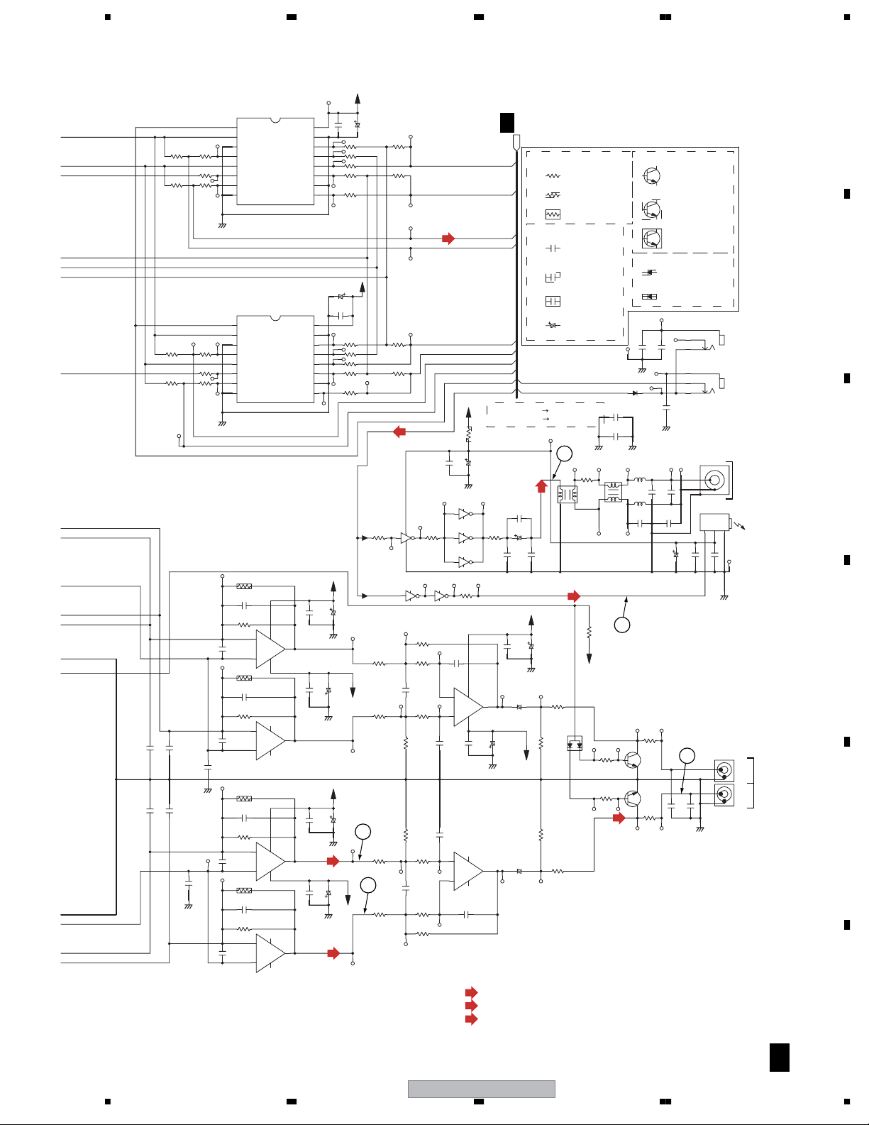
5678
*56
R1603
*
R1613 R1614
*56
R1615
*
*
*
C1202
C1201
*
*
C1101
C1102
GNDA
C1103
IC1601
TC74VHC157FTS1
1
SELECT
2
1A
3
R1602R1601
R1605
R1604
R1560
R1616
GNDA
*
1B
4
1Y 4B
5
2A
6
2B
22
7
2Y
8
56
GNDD
IC1602
TC74VHC157FTS1
1
SELECT VCC
2
1A
314
1B 4A
4
1Y
5
2A
6
2B
22
7
2Y 3B
89
GND
56
GNDD
R1214
330(D)
PCN1041
C1204
CH
1500p
R1201
*
2
-
*
3
+
R1215
330(D)
PCN1041
C1205
CH
1500p
R1202
*
6
-
*
C1220 C1219
5
+
*
C1203
R1114
330(D)
PCN1041
C1104
CH
1500p
R1101
*
2
-
*
C1119
3
+
R1115
PCN1041
330(D)
C1105
CH
1500p
R1102
*
6
-
*
C1120
5
+
VCC
ST
4A
4Y
Lch
3A
3B
PCM/DSD SEL
3YGND
ST
4B
Rch
4Y
3A
PCM/DSD SEL
3Y
C1206
8
1
(1/2)
IC1201
4
NJM5532MD
C1208
8
7
(2/2)
IC1201
4
NJM5532MD
C1106
8
1
(1/2)
IC1101
4
NJM5532MD
C1108
8
7
(2/2)
IC1101
4
NJM5532MD
16
15
14
13
12
11
10
9
16
15
13
12
11
10
(L)
0.1
C1209
0.1
GNDA
0.1
C1109
0.1
GNDA
(L)
V+12A
GNDA
V+12A
GNDA
C1601
C1605
47/35
C1603
C1207
100/16
V-12A
C1107
100/16
V+3D
YF1
47/35
C1602
R1608
22
R1606
10 *
R1607
R1609
100
R1611
R1610
10
R1612
56
V+3D
YF1
R1617
22
R1618
R1620
100
R1621
10
R1623
56
100/16
100/16
V-12A
*
R1619
10 *
R1622
*
(1/6)
IC1701
TC74VHCU04FT
14
R1702
1
00
7
IC1701
13
R1203
1.2k(D)
C1210
R1204
1.2k(D)
8
R1103
1.2k(D)
8
C1110
R1104
1.2k(D)
(AD)
(D)
C1704
IC1701
IC1701
R1703 R1704
2
IC1701
IC1701
(6/6) (5/6)
14
14
12
10
11
7
7
R1208
1.2k(D)
C1212
R1207
1.8k(D)
470p
CH
CH
6
1200p
R1206
5
CH
1.8k(D)
1.2k(D)
1.2k(D)
R1106
1.8k(D)
CH
1200p
R1107
1.8k(D)
R1108
1.2k(D)
C1211
C1111
470p
CH
470p
3
2
R1205
R1105
(D)
(AD)
2/2C
XPCM
SPDIF
22
C1118
C1711
C1115
(2/2)
100/16
(1/2)
RESISTOR
1608 SIZE
2125 SIZE
DISCRETE TYPE
CAPACITOR
1608 SIZE
2125 SIZE
SROUT
SRIN
C1721 R1751(0 )
C1722 R1752(0 )
(D)
C1709
0.01
C1710
47/35
*
V+12A
0.1
C1116
GNDA
C1213
47/50
VCH1255
NP
R1209
V-12A
R1109
C1113
NP
47/50
VCH1255
RS1/16S***J
RS1/10S***J
CCSR***
CKSRYB***
CKSQ***
DISCRETE TYPE
CEAT***
10
R1706
L1701
5
314
VTL1172
*
C1712
(D)
100/16
R1211
750
3
22k
22k
R1111
750
PMCK/BCK
PBCK/GND_1
DATA/DSD_L_1
LRCK/GND_1
MCLK/BCK
PBCK/GND_2
LRCK/GND_2
DATA/DSD_L_2
*1
V+3D
0
R1701
(2125)
V+3SPDIF
0.1
C1705
330/6.3
VCH1248
GNDD
(4/6)
14
8
9
7
(2/6)
14
3
4
7
(3/6)
14
5
6
7
R1705
47
8
7
+
IC1102
4
NJM5532MD
0.1
C1117
GNDA
IC1102
NJM5532MD
4
+
1
-
8
C1112
470p
CH
(L)
: AUDIO SIGNAL ROUTE(Lch)
: DIGITAL SIGNAL ROUTE
: AUDIO DATA SIGNAL ROUTE
C1721
*1
C1722
*1
GNDS GNDD
L1702
75
14
2
PTL1017
*
R1213
V-12A
D1651
DAP202U
12
R1210
1k
2SD2114K(VW)
2SD2114K(VW)
R1110
1k
(L)
1SS355
3
10
B
B
TRANSISTOR
DIODE
C1751
GNDS
D1751
F1701
DTF1068
F1702
CTF1661
C1716
*
R1212
220
C
Q1201
E
E
Q1101
C
R1112
220
SOT-323 TYPE
SOT-346 TYPE
(UMD3,UMT3)
(SMD3,SMT3)
SOT-363 TYPE
(UMT6)
DISCRETE TYPE
SOD-323 TYPE
(UMD2)
DISCRETE TYPE
YB
YF
1
C1752
0.01
C1753
GNDS
*
C1713
C1714
C1717
1000p
C1214
0.1
*
C1708
*
JA1751
RKN10041
3
2
JA1752
RKN10041
3
2
JA1702
47/35
C1706
9
C1114
GNDA
SR-OUT
SR-IN
JA1701
VKB1097-
DIGITAL OUT
1
COAX & OPT
2
3
VKS1002
132
YF1
C1707
1000p
GNDD
JA1201
PKB1042-
1
R
2
1
L
2
*
JA1101
PKB1041-
A
B
C
D
Rch OUT
Lch OUT
E
F
56
PD-D6-J
C 1/2
27
7
8
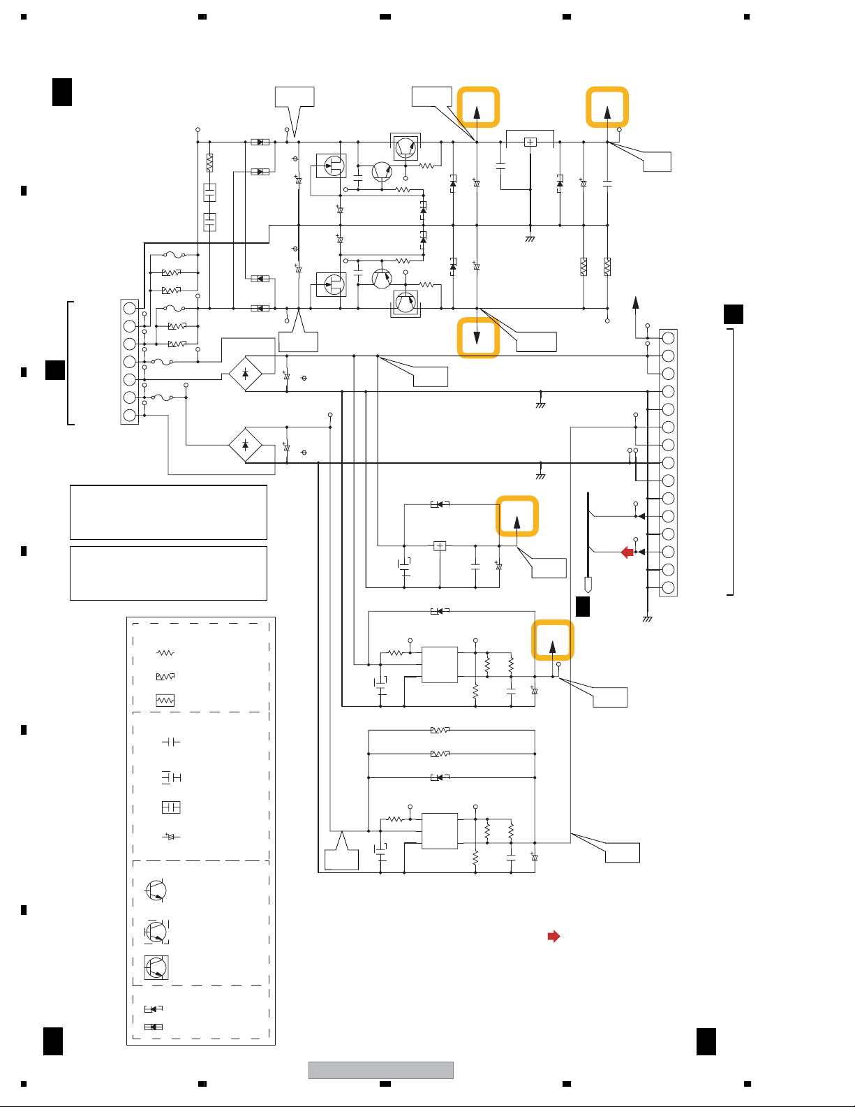
1234
3.6 AJKB ASSY (2/2)
A
B
C
D
E
C 2/2
J52
J
(AWM8075)
C1802 C1801
*
IC1801
(2125)
R1808
0
(2125)
CN1801
S7B-EH
AUDIO CT
AUDIO1
AUDIO2
DIGITAL1
DIGITAL2
MECHA1
MECHA2
CAUTION : FOR CONTINUED PROTECTION
MFD, BY LITTELFUSE INC.
CAUTION : FOR CONTINUED PROTECTION
MFD, BY LITTELFUSE INC.
R1809
0
IC1802 D1804
7
6
5
4
3
2
1
AGAINST RISK OF FIRE.
REPLACE ONLY WITH SAME TYPE
NO. 491003.HXR FOR IC1851
AGAINST RISK OF FIRE.
REPLACE ONLY WITH SAME TYPE
NO. 491004.HXR FOR IC1852
RESISTOR
1608 SIZE
2125 SIZE
DISCRETE TYPE
CAPACITOR
TRANSISTOR
*
R1810
(2125)0
(2125)
R1811
0
>
IC1851
AEK7015(3A)
IC1852
AEK7018
(4A)
>
RS1/16S***J
RS1/10S***J
RD1/4MUF***J
RS2LMF***J
1608 SIZE
CCSR***
CKSRYB***
2125 SIZE
CKSQ***
DISCRETE TYPE
SOT-323 TYPE
SOT-346 TYPE
(UMD3,UMT3)
(SMD3,SMT3)
SOT-363 TYPE
(UMT6)
CEAT***
AJKB ASSY
+17.2V
C1803
C1804
-17.2V
3300/25
C1852
4700/25
C1854
Q1801
4700/25
G
PCH1156
4700/25
18 18
PCH1156
G
Q1804
2SK246(Y)
1616
D
S
100/16
C1805
100/16
C1806
D
S
D1801
VAC3 +VCC
11EQS10 2SK246(Y)
D1802
4.7
R1801
11EQS10
ACE7063
0.56
0.56
ACE7063
D1803
11EQS10
VAC4
11EQS10
D1851
1
+
2
3
~
~
-
4
S1VB20/F03
D1852
1
+
23
~
~
-
4
D3SBA20(B)
+11V
Q1803
2SD1763A
C
E
*
R1803
B
C1815
Q1802
2SC3906K(RS)
2SA1514K(RS)
C1816
-VCC
330
R1805
Q1805
330
B
*
E
C
CE
Q1806
2SB1186A
C1831
R1835
1k
YF1
C1834
R1839
1k
YF1
C1837
(2125)
(2125)
+10.8V
EC
B
R1802
680
R1804
B
680
PNS1043
PNS1043
D1807
RB501V-40
D1805
UDZS12(B)
D1806
UDZS12(B)
D1808
RB501V-40
V+12A
C1807
C1808
V-12A
+8.3V
D1831
RB501V-40
IC1831
BD7802FP
OUTIN
13
2
YF1
(2125)
D1832
RB501V-40
IC1832
BA3948FP
1
5
2
34
R1843
*
R1844
*
D1833
RB501V-40
IC1833
1
5
2
3
4
R1840
BA00BC0WCP-V5
100/25
100/25
*
C1833
R1836
33k(F)
R1841
39k(F)
IC1804
NJM78M05FA
C1809
GNDA
V+3D
C1832
470/16
R1837
R1838
*
120k(F)
C1836
R1842
330k
330k
C1839
OUTIN
31
2
0.1
-10.8V
GNDD
GNDM
+3.3V
V+58U
C1835
100/16
*
C1838
100/16
*
(D)
V+5A
PNC-457-
+5V
C1811
YF
D1809
C1813
RB501V-40
R1806
1.0
1000/16 HAZL
R1807
330 2W
330 2W
V+12A
DVDMUTE
(D)
SPDIF
CN1851
CKS3380-
1/2C
GNDD
+5.8V
+6.5V
: DIGITAL SIGNAL ROUTE
1
2
3
4
5
6
7
8
9
10
11
12
13
14
15
CN2702
H
V+12A
V+9D
V+9D
GNDD
GNDD
V+6R5V
V+6R5V
GNDM
GNDM
GNDD
DVDMUTE
GNDD
DOUT
GNDD
GNDD
F
28
C 2/2
DISCRETE TYPE
DIODE
SOD-323 TYPE
(UMD2)
DISCRETE TYPE
C 2/2
PD-D6-J
1234

5678
A
B
C
D
E
56
PD-D6-J
F
29
7
8
 Loading...