

Page 1
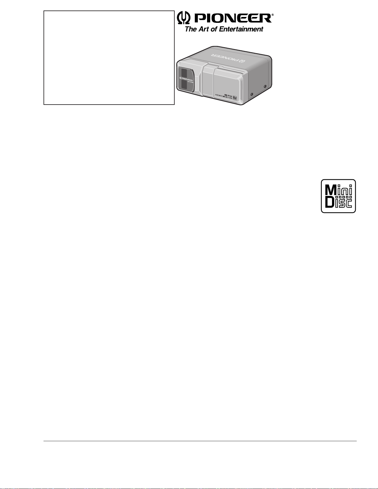
6-DISC MULTI-MINI DISC PLAYER
MD-P100 EW
Se
r
vic
e
M
a
nu
a
l
PIONEER ELECTRONIC CORPORATION 4-1, Meguro 1-Chome, Meguro-ku, Tokyo 153-8654, Japan
PIONEER ELECTRONICS SERVICE INC. P.O.Box 1760, Long Beach, CA 90801-1760 U.S.A.
PIONEER ELECTRONIC [EUROPE] N.V. Haven 1087 Keetberglaan 1, 9120 Melsele, Belgium
PIONEER ELECTRONICS ASIACENTRE PTE.LTD. 501 Orchard Road, #10-00, Lane Wheelock Place, Singapore 23880
C PIONEER ELECTRONIC CORPORATION 1998
ORDER NO.
CRT2203
CONTENTS
1. SAFETY INFORMATION ............................................2
2. EXPLODED VIEWS AND PARTS LIST.......................2
3. SCHEMATIC DIAGRAM .............................................8
4. PCB CONNECTION DIAGRAM ................................18
5. ELECTRICAL PARTS LIST ........................................26
6. ADJUSTMENT..........................................................29
7. GENERAL INFORMATION .......................................30
7.1 IC .........................................................................30
7.2 DISASSEMBLY ...................................................40
7.3 BLOCK DIAGRAM ..............................................44
8. OPERATIONS AND SPECIFICATIONS.....................46
- US and foreign patents licensed from Dolby Laboratories Licensing Corporation.
K-FEA. APR. 1998 Printed in Japan
Page 2
2
MD-P100
1. SAFETY INFORMATION
This service manual is intended for qualified service technicians; it is not meant for the casual do-it-yourselfer.
Qualified technicians have the necessary test equipment and tools, and have been trained to properly and safely repair
complex products such as those covered by this manual.
Improperly performed repairs can adversely affect the safety and reliability of the product and may void the warranty.
If you are not qualified to perform the repair of this product properly and safely; you should not risk trying to do so
and refer the repair to a qualified service technician.
2. EXPLODED VIEWS AND PARTS LIST
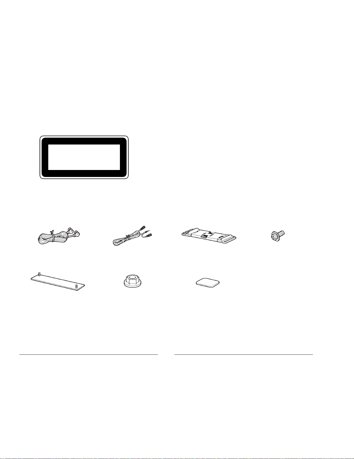
2.1 PACKING
A “CLASS 1 LASER PRODUCT” label is affixed to the
rear of the player.
CLASS 1
LASER PRODUCT
- PACKING SECTION PARTS LIST
Mark No. Description Part No. Part No.
(PIONEER) (SONY)
Mark No. Description Part No. Part No.
(PIONEER) (SONY)
NOTE:
- Parts marked by "*"are generally unavailable because they are not in our Master Spare Parts List.
- Screws adjacent to ∇ mark on the product are used for disassembly.
1 Cord CZD3030 177777311
2 Cord CZD3036 177777421
3 Base CZN5122 393016311
4 PSW CZB3044 768296101
5
Installation Base Assy CZX3015 X33711782
6 Nut CZB3043 430451111
7 Cushion CZN5092 393016601
Cushion F CZN5090 393561001
Cushion R CZN5091 393561101
Owner's Manual CZR3024 386206311
(English, Spanish, German)
Owner's Manual CZR3025 386206321
(French, Italian, Dutch)
Installation ManualCZR3026 386206411
(English, Spanish, German, French, Italian, Dutch)
* Warranty Card CZR3027 302285101
Carton CZH3047 302510901
Contain Box CZH3048 302511001
5 6
7
1 2 3 4
Page 3

3
MD-P100
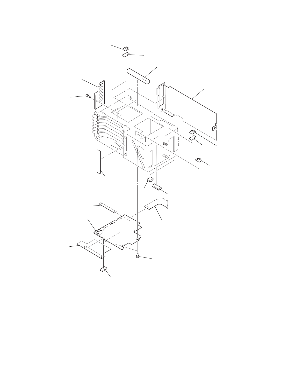
2.2 EXTERIOR
1 Door Assy CZX3010 X33727481
2 Door Assy CZX3067 X33752241
3 PCB CZN5082 166294111
4 •••••
5 Front Panel Assy CZX3068 X33752251
6 Lamp PCB CZN5081 165888613
7 Screw CZB3036 390941201
8 Case(Upper) CZN5143 302296101
9 Cover CZN5086 393980701
10 Rear Panel Assy CZX3012 X33727471
11 Power PCB Assy CZW3061 A3222982A
12 Damper CZN5071 393017601
13 Spring CZB3038 393017701
14 Case(Lower) CZN5142 393017391
15 Cushion CZN5085 393169701
16 Cushion CZN5068 334875003
17 Cord CZD3037 177777221
18
Self-Tapping Screw CZB3041 768510411
19
Self-Tapping Screw CZB3042 768513311
20 PTT CZB3039 762177560
21 BVTT CZB3037 391295611
22 Sheet CZN5080 393374001
23 Cushion CZN5079 383144111
24 Spacer CZN5117 393074401
25 Cushion CZN5068 334875003
- EXTERIOR SECTION PARTS LIST
Mark No. Description Part No. Part No.
(PIONEER) (SONY)
Mark No. Description Part No. Part No.
(PIONEER) (SONY)
Page 4
9
8
7
6
5
4
3
2
1
12
not supplied
11
6
10
not supplied
6
7
6
4
MD-P100
2.3 MAIN PCB
1 Sheet CZN5073 393114901
2 Main PCB CZW3057 A3294102A
3 Cable CZD3029 177647411
4 Screw CZB3036 390941201
5 Sensor PCB CZN5087 165888413
6 Cushion CZN5068 334875003
7 Cushion CZN5069 371597301
8 Cushion CZN5075 393169901
9 Sheet CZN5072 393102503
10 Cushion CZN5074 393169801
11 PCB CZN3100 166294211
12 Screw CZB3073 302397401
- MAIN PCB SECTION PARTS LIST
Mark No. Description Part No. Part No.
(PIONEER) (SONY)
Mark No. Description Part No. Part No.
(PIONEER) (SONY)
Page 5
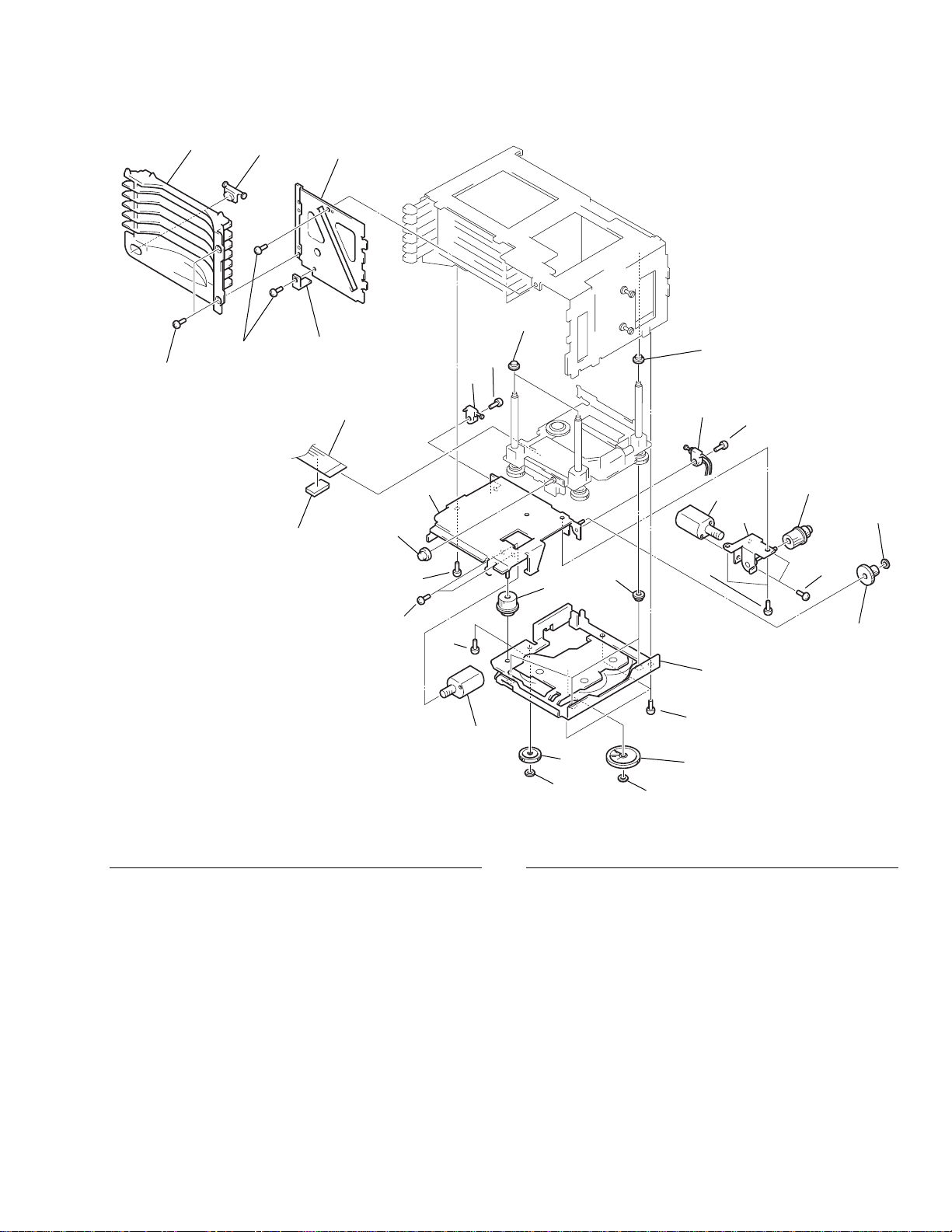
1 Screw CZB3046 331755271
2 Escutcheon CZN5098 393031413
3 Button(Stop) CZA3022 393031902
4 Chassis(Front) CZN5100 393032002
5 Plate CZN5102 393136601
6 PCB CZN5093 165888112
7
Chassis(Motor)Assy CZX3069 X33746691
8 Collar CZL3004 393031001
9 Bearing CZN5096 393031202
10 Plate(LD2)Assy CZX3071 X33746731
11 Worm Wheel CZN5116 393036501
12 Washer CZB3065 337771911
13 Gear(LD) CZN5113 393031701
14
Chassis(Bottom A)Assy CZX3065 X33755301
15 Gear CZN5097 393031301
16 Gear(ELV2) CZN5145 302038601
17
Worm Wheel(ELV2) CZN5147 302036301
18 Switch CZS3038 157077111
19 Switch CZS3039 157077121
20 Screw CZB3048 762785237
21 Screw CZB3049 762755407
22 Screw CZB3059 762785507
23 LD Motor Assy CZX3076 X33715082
24 ELV Motor Assy CZX3077 X33748121
2
3
4
1
1
5
6
7
24
not supplied
8
17
9
10
11
9
9
12
13
14
19
16
12
12
15
20
20
20
21
22
18
20
22
21
23
5
MD-P100
2.4 MD(1)
- MD(1) SECTION PARTS LIST
Mark No. Description Part No. Part No.
(PIONEER) (SONY)
Mark No. Description Part No. Part No.
(PIONEER) (SONY)
Page 6
1 Chassis Assy CZX3034 X33712093
2 Guide(Holder 2) CZN5144 302038801
3 Button(EJECT) CZA3023 393031801
4 Button(EJECT) CZA3024 393031811
5 Button(EJECT) CZA3025 393031821
6 Button(EJECT) CZA3026 393031831
7 Button(EJECT) CZA3027 393031841
8 Button(EJECT) CZA3028 393031851
9 Eject Lever CZN5112 393035401
10 Washer CZB3065 337771911
11 Spring(EJ) CZB3063 393035002
12
Holder(Caddie)Assy CZX3026 X33712165
13 Spring(D Lock) CZB3064 393035202
14
Loading Slider 2 Assy CZX3070 X33746722
15 Rack(Loading) CZN5115 393036601
16 Spring CZB3068 393036001
17
Chassis(Rear 2)Assy CZX3064 X33746712
18 Spring(Lock) CZB3062 393034901
19 Plate(Holder)Assy CZX3027 X33712195
20 Washer CZN5111 302151101
21 Screw CZB3048 762785237
- MD(2) SECTION PARTS LIST
Mark No. Description Part No. Part No.
(PIONEER) (SONY)
Mark No. Description Part No. Part No.
(PIONEER) (SONY)
13
1
21
2
3
4
5
6
7
8
9
10
11
12
12
20
19
18
17
14
16
15
10
6
MD-P100
2.5 MD(2)
Page 7

7
6
33
30
4
3
27
2
1
23
22
19
21
20
32
14
12
11
5
10
9
8
13
15
24
16
30
30
25
30
29
29
28
26
32
31
30
17
18
7
6
33
1 Holder CZN5106 393033801
2 Guide(OPB) CZL3003 393033201
3 Screw Assy CZX3037 X33712122
4 PCB CZN5064 165888011
5 Sleeve(ELV) CZN5103 393033302
6 Spring(ELV) CZB3051 393033401
7 ELV Limiter Plate BCZN5110 393034501
8 Chassis(OP)Assy CZX3024 X33712152
9 ELV Limiter Plate ACZN5109 393034402
10 Spring CZB3053 393071101
11 Worm Wheel CZN5107 393033901
12 Washer CZB3050 333864531
13 Screw CZB3070 393034301
14 Plate CZN5108 393034202
15 Holder(SLB) CZN5104 393033601
16 Spring CZB3052 393033501
17 Holder CZX3022 X33712131
18 Screw CZX3023 X33712141
19 Guide(OPA) CZL3002 393033101
20 Spring CZN5105 393033701
21 Mini Disc Device CZG3005 858303501
22 Servo PCB Assy CZW3054 A3222980A
23 Screw CZB3054 393275501
24 SP Motor CZX3019 A3291507A
25 SL Motor Assy CZX3020 A3291508A
26
Slide Variable Resistor CZC5118 122381712
27 Switch CZS3039 157077121
28 Screw CZB3059 762785507
29 Screw CZB3056 762785227
30 Screw CZB3055 762755218
31 Screw CZB3058 762785258
32 Screw CZB3048 762785237
33 Sleeve(ELV2) CZN5146 302035101
- MD(3) SECTION PARTS LIST
Mark No. Description Part No. Part No.
(PIONEER) (SONY)
Mark No. Description Part No. Part No.
(PIONEER) (SONY)
7
MD-P100
2.6 MD(3)
Page 8
8
MD-P100
1
23
4
1234
D
C
B
A
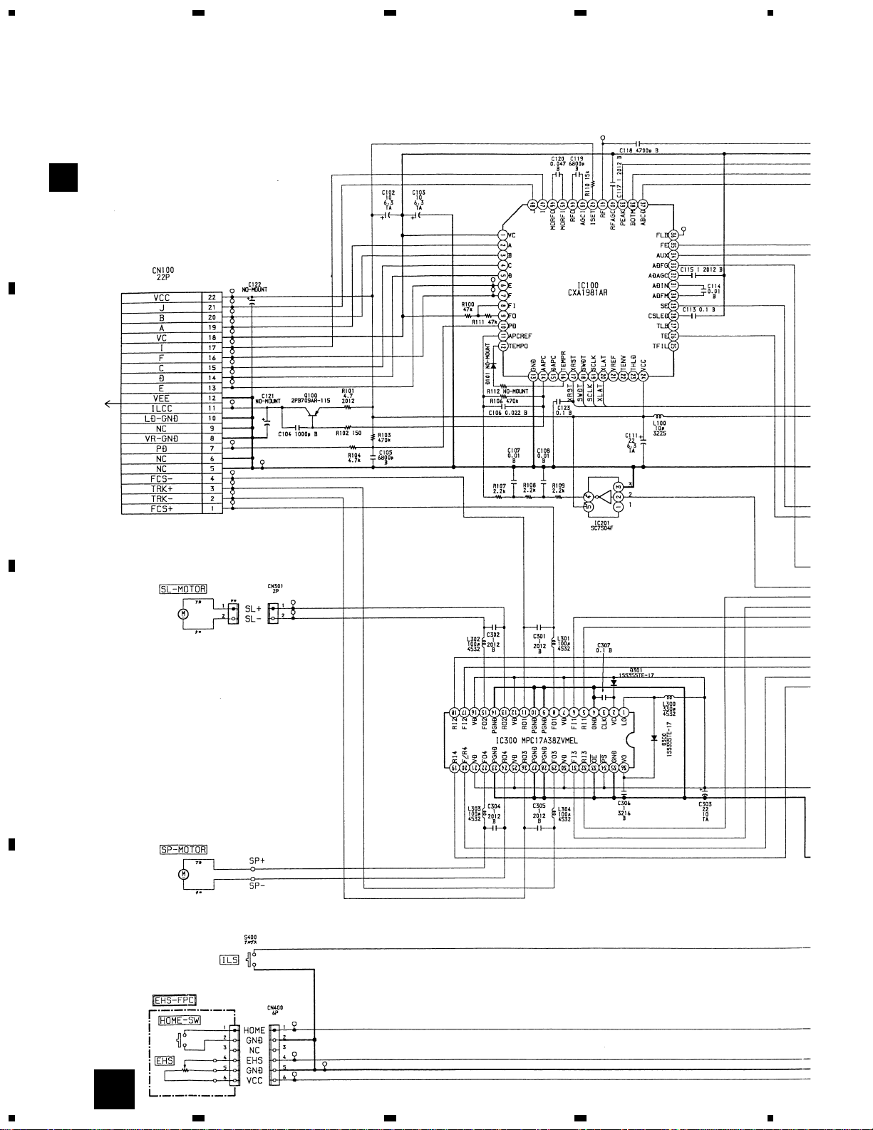
3. SCHEMATIC DIAGRAM
3.1 SERVO PCB ASSY
A
SERVO PCB ASSY
A
MINI DISC DEVICE
Page 9
9
MD-P100
5
6
78
5
6
78
D
C
B
A
Note: When ordering service parts, be sure to refer to “EXPLODED VIEWS AND PARTS LIST” or “ELECTRICAL PARTS
LIST”.
A
B
CN500
Page 10
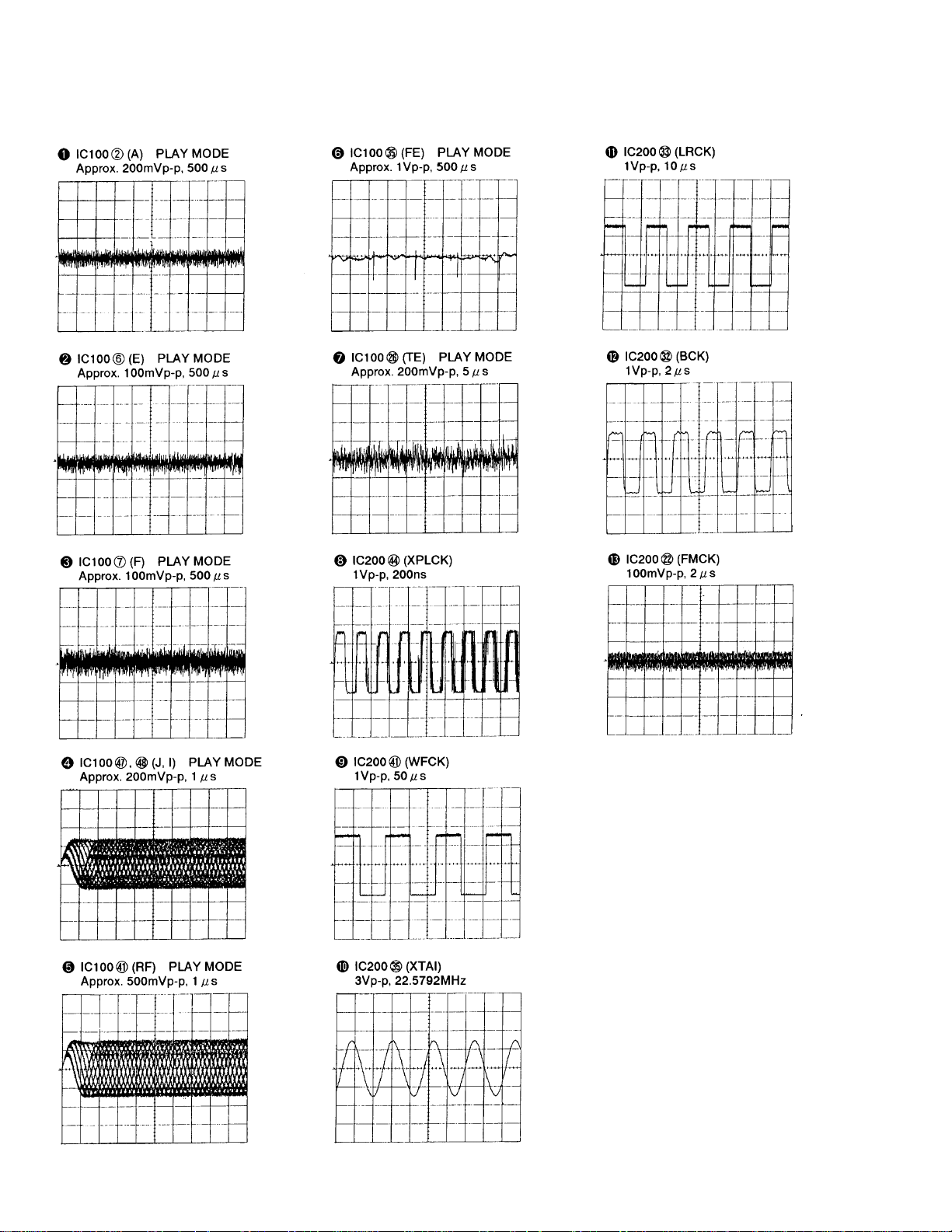
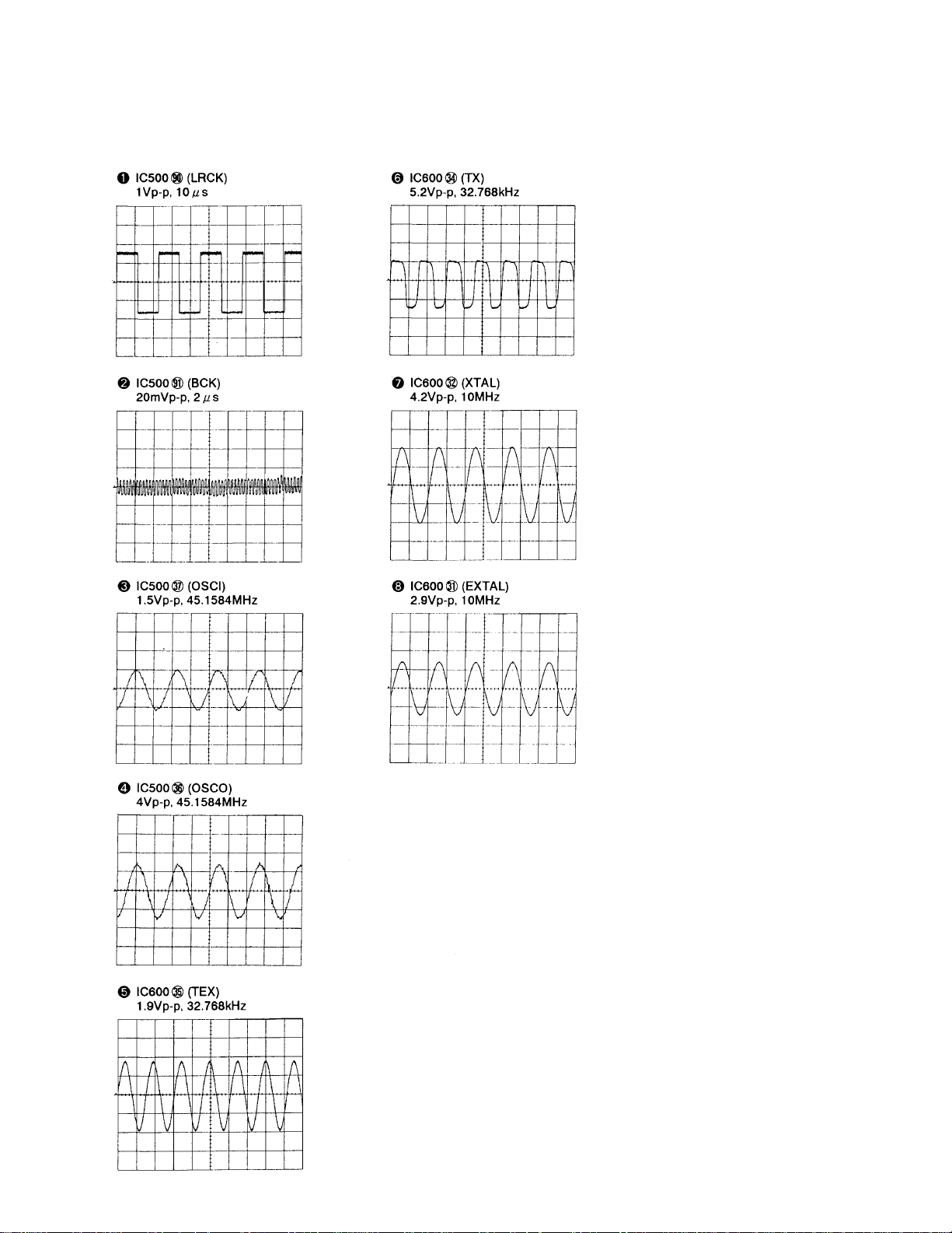
- Waveforms
10
MD-P100
Page 11
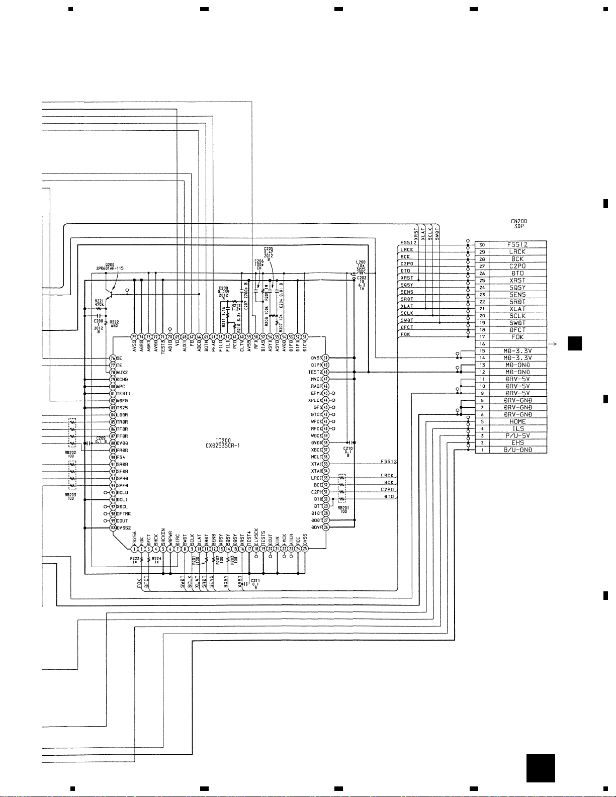
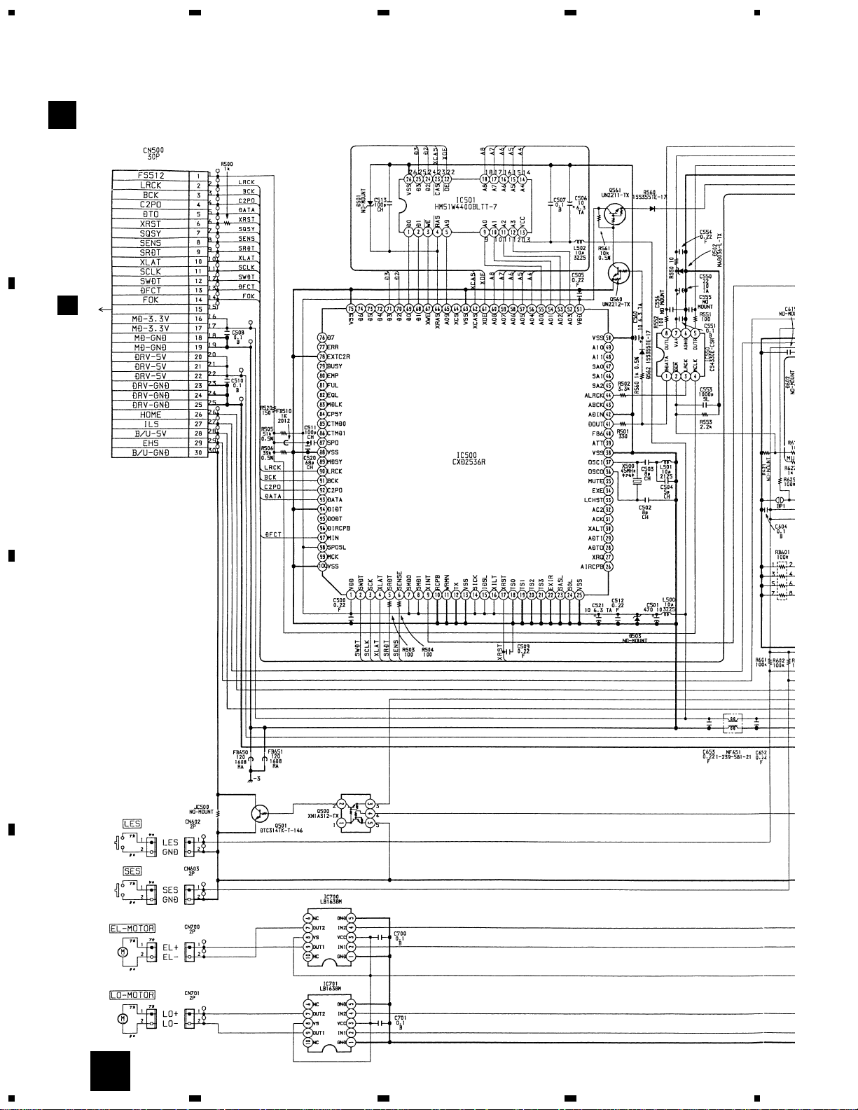
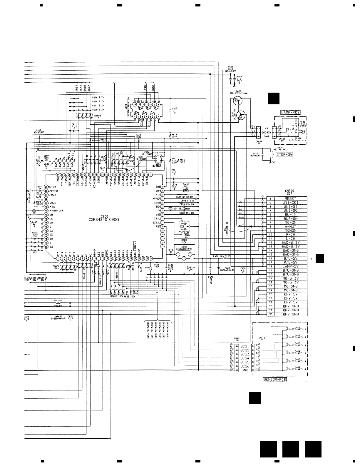
3.2 MAIN PCB
- Waveforms
11
MD-P100
Page 12
12
MD-P100
1
23
4
1234
D
C
B
A
CN200
A
MAIN PCB
B
B
Page 13
13
MD-P100
5
6
78
5
6
78
D
C
B
A
CN5
B
SENSOR MOUNT PCB
D
D
LAMP MOUNT PCB
C
C
E
Page 14
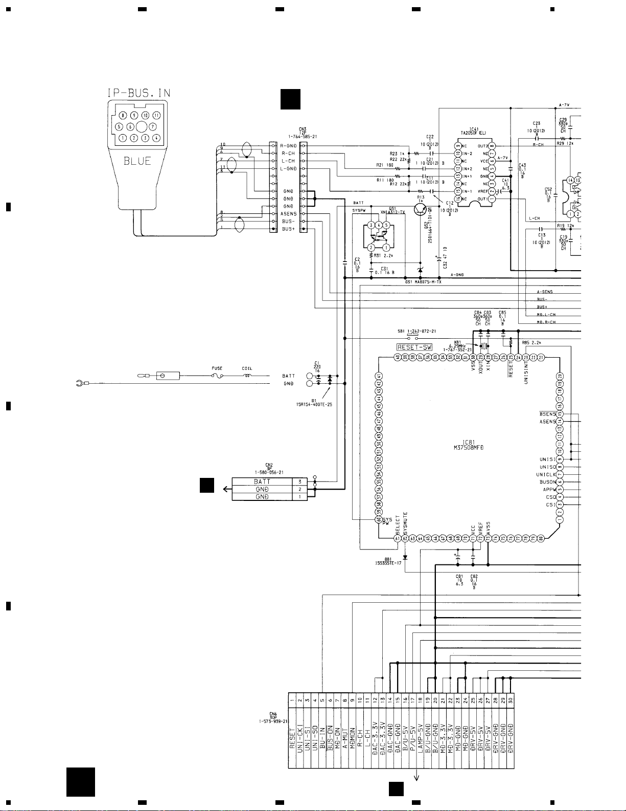
3.3 I/F MOUNT ASSY
I/F MOUNT ASSY
CN900
CN800
MD-P100
1
23
4
1234
D
C
B
A
14
E
E
F
F
Page 15
CN600
B
15
MD-P100
5
6
78
5
6
78
D
C
B
A
E
Page 16

3.4 POWER PCB ASSY
POWER PCB ASSY
CN2
MD-P100
1
23
4
1234
D
C
B
A
16
F
F
E
Page 17

CN6
17
MD-P100
5
6
78
5
6
78
D
C
B
A
F
E
Page 18

18
MD-P100
1
23
4
1234
D
C
B
A
SIDE A
4. PCB CONNECTION DIAGRAM
4.1 POWER PCB ASSY
Capacitor
Connector
P.C.Board
Chip Part
SIDE A
SIDE B
NOTE FOR PCB DIAGRAMS
1. The parts mounted on this PCB
include all necessary parts for
several destination.
For further information for
respective destinations, be sure
to check with the schematic dia-
gram.
2. Viewpoint of PCB diagrams
POWER PCB ASSY
IC,Q
Q910
IC900
Q911
Q820
Q800
Q810
IC800
Q921
Q920
Q941
Q940
Q931
Q954
Q950
Q953
IC950
Q952
F
F
CN2
E
CN6
E
Page 19

MD-P100
D
C
B
A
1
2
34
1
2
34
SIDE B
19
POWER PCB ASSY
F
F
Page 20

20
MD-P100
1
23
4
1234
D
C
B
A
SIDE A
SERVO PCB ASSY
4.2 SERVO PCB ASSY
A
A
IC,Q
IC200
Q200
IC300
IC201
IC100
Q100
B
CN500
MINI DISC
DEVICE
Page 21

21
MD-P100
D
C
B
A
1
2
34
1
2
34
SIDE B
SERVO PCB ASSY
A
A
Page 22

MAIN PCB
SIDE A
IC,Q
IC700
IC600
IC701
IC602
Q601
IC550
Q600
Q500
Q501
IC500
IC501
22
MD-P100
1
23
4
1234
D
C
B
A
SENSOR MOUNT PCB
LAMP MOUNT PCB
B
D
C
4.3 MAIN PCB, LAMP MOUNT PCB, SENSOR MOUNT PCB
D
C
CN200
A
CN610
D
CN5
E
CN620
C
CN601
B
CN604
B
B
Page 23

23
MD-P100
D
C
B
A
1
2
34
1
2
34
SIDE B
IC,Q
IC601
Q560
Q561
MAIN PCB
B
LAMP MOUNT PCB
C
SENSOR MOUNT PCB
D
B
D
C
Page 24

24
MD-P100
1
23
4
1234
D
C
B
A
4.4 I/F MOUNT ASSY
SIDE A
Q21
Q11
IC81
IC71
Q71
Q32
Q52
IC51
IC41
I/F MOUNT ASSY
E
E
IC,Q
CN900
F
CN800
F
Page 25

25
MD-P100
D
C
B
A
1
2
34
1
2
34
SIDE B
Q31
Q51
Q53
I/F MOUNT ASSY
E
E
IC,Q
CN600
B
Page 26

26
MD-P100
=Circuit Symbol and No.=Part Name Part No. Part No.
(PIONEER) (SONY)
--- --- ------------ ------------ ------------
Unit Number :
Unit Name : I/F Mount Assy
MISCELLANEOUS
IC 41 IC TA2050F 875926237
IC 51 IC BA3129F 875935295
IC 71 IC HA1287FP 875944209
IC 81 IC PD5403B 875953715
Q 11 Transistor DTC314TK 872992022
Q 21 Transistor DTC314TK 872992022
Q 31 Transistor XN1A312-TX 872902067
Q 32 Transistor 2SD1664 872992087
Q 51 Transistor DTC124EK 872902752
Q 52 Transistor DTA144TKA 872902739
Q 53 Transistor FMC4A 872903630
Q 71 Transistor 2SC2412K 872992075
D 1 Diode 1SR154-400 871905318
D 31 Diode MA8075(M) 871942277
D 81 Diode 1SS355 871998861
X 81 Radiator 6.29MHz CZS3048 176735221
S 81 Keyboard Switch CZS3046 157248461
CN 2 Connector CZK3059 158005621
CN 3 Connector CZK3058 176458521
CN 4 Connector CZK3058 176458521
CN 5 Connector CZK3064 175036121
CN 6 Connector CZK3057 157393921
RESISTORS
R 11 RS1/16S181J 121681291
R 12 RS1/16S223J 121683791
R 13 RS1/16S102J 121682191
R 14 RS1/16S473J 121684191
R 15 RS1/16S473J 121684191
R 16 RS1/16S473J 121684191
R 17 RS1/16S821J 121682091
R 18 RS1/16S104J 121684591
R 19 RS1/16S123J 121683491
R 21 RS1/16S181J 121681291
R 22 RS1/16S223J 121683791
R 23 RS1/16S102J 121682191
R 24 RS1/16S473J 121684191
R 25 RS1/16S473J 121684191
R 26 RS1/16S473J 121684191
R 27 RS1/16S821J 121682091
R 28 RS1/16S104J 121684591
R 29 RS1/16S123J 121683491
R 31 RS1/16S222J 121682591
R 51 RS1/16S222J 121682591
R 52 RS1/16S222J 121682591
R 53 RS1/16S104J 121684591
R 54 RS1/16S473J 121684191
R 55 RS1/16S473J 121684191
R 71 RS1/16S101J 121680991
R 72 RS1/16S104J 121684591
R 73 RS1/16S101J 121680991
R 74 RS1/16S104J 121684591
R 75 RS1/16S101J 121680991
R 76 RS1/16S101J 121680991
R 77 RS1/16S101J 121680991
R 78 RS1/16S473J 121684191
R 79 RS1/16S104J 121684591
R 81 RS1/16S473J 121684191
R 82 RS1/16S473J 121684191
R 83 RS1/16S473J 121684191
R 84 RS1/16S102J 121682191
R 85 RS1/16S222J 121682591
R 86 RS1/10S223J 121608191
R 87 RS1/10S223J 121608191
CAPACITORS
C 1 CZC5144 112693491
C 2 CZC5142 110782691
C 11 CZC5146 110998291
C 12 CZC5146 110998291
C 13 CZC5143 110998291
C 14 CZC5148 111044621
C 15 CCSRCH361J50 116439191
C 17 CZC5146 110998291
C 19 CZC5167 116439091
C 21 CZC5146 110998291
C 22 CZC5146 110998291
C 23 CZC5143 110998291
C 24 CZC5148 111044621
C 25 CCSRCH361J50 116439191
C 27 CZC5146 110998291
C 29 CZC5167 116439091
C 31 CZC5142 110782691
C 32 CZC5149 111045221
C 41 CZC5148 111044621
C 43 CZC5142 110782691
C 52 CZC5145 110782691
C 53 CZC5147 111044421
C 54 CZC5142 110782691
C 73 CZC5145 110782691
C 81 CZC5148 111044621
C 82 CZC5145 110782691
C 83 CZC5166 116292191
C 84 CZC5166 116292191
C 85 CZC5142 110782691
Unit Number : CZW3054
Unit Name : Servo PCB Assy
MISCELLANEOUS
IC 100 IC CXA1981AR 875207268
IC 200 IC CXD2535CR-1 875238223
IC 201 IC SC7S04F 875903184
IC 300 IC MPC17A38VMEL 875917960
Q 100 Transistor 2SA1037K 872902648
5. ELECTRICAL PARTS LIST
NOTES:
- Parts whose parts numbers are omitted are subject to being not supplied.
- The part numbers shown below indicate chip components.
Chip Resistor
RS1/_S___J,RS1/__S___J
Chip Capacitor (except for CQS.....)
CKS....., CCS....., CSZS.....
A
E
=Circuit Symbol and No.=Part Name Part No. Part No.
(PIONEER) (SONY)
--- --- ------------ ------------ ------------
Page 27

Q 200 Transistor 2SC2712 872923049
D 300 Diode 1SS355 871998862
D 301 Diode 1SS355 871998862
L 100 Inductor CZT3086 141205821
L 200 Inductor CZT3086 141205821
L 300 Micro-Inductor CZT3085 141203941
L 301 Micro-Inductor CZT3085 141203941
L 302 Micro-Inductor CZT3085 141203941
L 303 Micro-Inductor CZT3085 141203941
L 304 Micro-Inductor CZT3085 141203941
S 400 Push Switch CZS3041 169253221
RB 201 Chip Network Resistor CZC5119 123357621
RB 202 Chip Network Resistor CZC5119 123357621
RB 203 Chip Network Resistor CZC5119 123357621
CN 100 Connector CZK3048 157393121
CN 200 Connector CZK3047 157337021
CN 301 Connector Pin 2P CZK3045 158005521
CN 400 Connector CZK3046 157334621
RESISTORS
R 100 RS1/16S473J 121684191
R 101 RS1/10S4R7J 121630891
R 102 RS1/16S151J 121681191
R 103 RS1/16S474J 121685391
R 104 RS1/16S472J 121682991
R 106 RS1/16S474J 121685391
R 107 RS1/16S222J 121682591
R 108 RS1/16S222J 121682591
R 109 RS1/16S222J 121682591
R 110 RS1/16S153J 121683591
R 111 RS1/16S473J 121684191
R 201 RS1/16S101J 121680991
R 202 RS1/16S101J 121680991
R 203 RS1/16S101J 121680991
R 207 RS1/16S103J 121683391
R 208 RS1/16S104J 121684591
R 209 RS1/16S105J 121685791
R 210 RS1/16S332J 121682791
R 211 RS1/16S112J 121827091
R 212 RS1/16S122J 121682291
R 221 RS1/16S474J 121685391
R 222 RS1/16S681J 121681991
R 223 RS1/16S102J 121682191
R 224 RS1/16S102J 121682191
CAPACITORS
C 102 CZC5123 113525991
C 103 CZC5123 113525991
C 104 CKSRYB102K50 116296491
C 105 CKSRYB682K25 116296991
C 106 CKSRYB223K25 116422711
C 107 CKSRYB103K25 116297011
C 108 CKSRYB103K25 116297011
C 111 CZC5120 110485211
C 113 CZC5122 110782691
C 114 CKSRYB103K25 116297011
C 115 CKSQYB105K10 110998291
C 117 CKSQYB105K10 110998291
C 118 CKSRYB472K50 116296891
C 119 CKSRYB682K25 116296991
C 120 CKSRYB473K16 116517691
C 123 CZC5122 110782691
C 200 CKSQYB105K10 110998291
C 202 CZC5123 113525991
C 204 CKSRYB103K25 116297011
C 205 CKSQYB474K16 110782391
C 206 CCSRCH101J50 116292791
C 207 CKSRYB272K50 116297991
C 208 CKSQYB393K25 116258791
C 209 CZC5122 110782691
C 210 CZC5122 110782691
C 211 CZC5122 110782691
C 301 CKSQYB105K10 110998291
C 302 CKSQYB105K10 110998291
C 303 CZC5121 110485291
C 304 CKSQYB105K10 110998291
C 305 CKSQYB105K10 110998291
C 306 CZC5122 110782691
C 307 CZC5122 110782691
Unit Number : CZW3057
Unit Name : Main PCB
MISCELLANEOUS
IC 500 IC CXD2536R 875237117
IC 501 IC HM51W4400TT6-8 875934128
IC 550 IC CS4330E-CSR 875936229
IC 600 IC CXP84340-090Q 875289373
IC 601 IC XC61AN4002PR 875936381
IC 602 IC TC74HCT7007AF(EL) 875923847
IC 700 IC LB1638M 875982387
IC 701 IC LB1638M 875982387
Q 500 Transistor XN1A312-TX 872902067
Q 501 Transistor DTC314TK 872992021
Q 560 Transistor UN2212 872942459
Q 561 Transistor UN2211 872942122
Q 600 Transistor DTB113ZK 872990460
Q 601 Transistor UN2211 872942122
D 502 Diode MA8036(L) 871942136
D 560 Diode 1SS355 871998862
D 561 Diode 1SS355 871998862
D 562 Diode 1SS355 871998862
D 600 Diode MA8062(M) 871942264
L 500 Inductor CZT3088 141205821
L 501 Inductor CZT3087 141099821
L 502 Inductor CZT3088 141205821
L 600 Inductor CZT3090 141205821
TH 600 Thermister CZC5125 181042121
X 500 Crystal Oscillator 45MHz CZS3043 176016821
X 600
Ceramic Oscillator 10MHz
CZS5124 176036521
X 601
Crystal Oscillator 32.768kHz
CZS3044 157988621
S 600 Keyboard Switch CZS3045 157191421
FB 510 Inductor CZT3091 141423521
FB 650 Ferrite Chip CZT3089 150023521
FB 651 Ferrite Chip CZT3089 150023521
NF 650 EMI Filter CZC5137 123946621
NF 651 EMI Filter CZC5138 123958121
RB 600 Resistor CZC5136 123381021
RB 601 Resistor CZC5165 123381021
RB 602 Resistor CZC5127 123357621
RB 603 Resistor CZC5135 123341221
RB 604 Resistor CZC5135 123341221
RB 605 Resistor CZC5136 123381021
RB 606 Resistor CZC5135 123341221
RB 607 Resistor CZC5135 123341221
RB 609 Resistor CZC5135 123341221
CN 500 Connector CZK3050 157337021
CN 600 Connector CZK3052 157393921
CN 601 Connector CZK3051 157391621
CN 602 Connector Pin CZK3053 158005521
CN 603 Connector Pin CZK3053 158005521
CN 604 Connector Pin CZK3056 158005621
CN 700 Connector Pin CZK3055 158005561
CN 701 Connector Pin CZK3054 158005541
RESISTORS
R 500 RS1/16S102J 121682191
R 501 RS1/16S331J 121681591
R 502 RS1/16S332J 121682791
R 503 RS1/16S101J 121680991
R 504 RS1/16S101J 121680991
27
MD-P100
=Circuit Symbol and No.=Part Name Part No. Part No.
(PIONEER) (SONY)
--- --- ------------ ------------ ------------
=Circuit Symbol and No.=Part Name Part No. Part No.
(PIONEER) (SONY)
--- --- ------------ ------------ ------------
B
Page 28

R 505 CZC5134 121873391
R 506 CZC5133 121873091
R 520 RS1/16S151J 121681191
R 550 RS1/16S100J 121679791
R 551 RS1/16S101J 121680991
R 552 RS1/16S101J 121680991
R 553 RS1/16S222J 121682591
R 560 CZC5131 121369291
R 561 CZC5132 121871691
R 600 RS1/16S473J 121684191
R 601 RS1/16S104J 121684591
R 602 RS1/16S104J 121684591
R 603 RS1/16S104J 121684591
R 605 RS1/16S104J 121684591
R 607 CZC5126 121870891
R 608 RS1/16S102J 121682191
R 609 RS1/16S222J 121682591
R 610 RS1/16S102J 121682191
R 611 RS1/16S222J 121682591
R 612 RS1/16S104J 121684591
R 613 RS1/16S102J 121682191
R 614 RS1/16S222J 121682591
R 615 RS1/16S102J 121682191
R 616 RS1/16S222J 121682591
R 617 RS1/16S104J 121684591
R 618 RS1/16S104J 121684591
R 619 RS1/16S103J 121683391
R 622 RS1/16S101J 121680991
R 624 RS1/16S102J 121682191
R 625 RS1/16S104J 121684591
R 626 RS1/16S104J 121684591
R 627 RS1/16S102J 121682191
R 628 RS1/16S104J 121684591
R 629 RS1/16S104J 121684591
R 630 RS1/16S473J 121684191
R 631 RS1/16S102J 121682191
R 632 RS1/16S102J 121682191
R 633 RS1/16S102J 121682191
CAPACITORS
C 500 CKSRYF224Z16 116512891
C 501 CZC5140 112836121
C 502 CCSRCH5R0C50 116291091
C 503 CKSRYB103K25 116297091
C 504 CCSRCH5R0C50 116291091
C 505 CKSRYF224Z16 116512891
C 506 CZC5130 113525991
C 507 CZC5129 110782691
C 508 CZC5129 110782691
C 509 CKSRYF224Z16 116512891
C 510 CZC5129 110782691
C 511 CCSRCH101J50 116292791
C 512 CKSRYF224Z16 116512891
C 513 CCSRCH101J50 116292791
C 520 CCSRCH680J50 116292591
C 521 CZC5141 113525991
C 550 CZC5128 110485291
C 551 CZC5129 110782691
C 553 CCSRSL102J50 116435791
C 554 CKSRYF224Z16 116512891
C 557 CKSQYB104K16 116400411
C 560 CZC5141 113525991
C 600 CZC5164 110485291
C 601 CKSRYF224Z16 116512891
C 602 CKSQYB224K16 116448991
C 603 CZC5139 110782691
C 604 CZC5139 110782691
C 605 CZC5129 110782691
C 607 CCSRCH101J50 116292791
C 608 CCSRCH150J50 116291791
C 609 CCSRCH150J50 116291791
C 610 CZC5139 110782691
C 611 CKSRYF224Z16 116512891
C 620 CZC5139 110782691
C 621 CZC5139 110782691
C 650 CKSRYF224Z16 116512891
C 651 CKSRYF224Z16 116512891
C 652 CKSRYF224Z16 116512891
C 653 CKSRYF224Z16 116512891
C 700 CZC5129 110782691
C 701 CZC5129 110782691
Unit Number : CZW3061
Unit Name : Power PCB Assy
MISCELLANEOUS
IC 800 IC NJM4580E 875971182
IC 900 IC MM1284XFFE 875928487
IC 950 IC TL1451ACDB-E20 875937013
Q 800 Transistor UN2112 872942412
Q 810 Transistor DTC314TK 872992021
Q 820 Transistor DTC314TK 872992021
Q 910 Transistor 2SD1664 872992085
Q 911 Transistor 2SD601A 872942227
Q 920 Transistor 2SD601A 872942227
Q 921 Transistor UN2112 872942412
Q 931 Transistor 2SD1664 872992085
Q 940 Transistor XN1A312-TX 872902067
Q 941 Transistor 2SD1664 872992085
Q 950 Transistor 2SB1115A-YQ 872910660
Q 952 Transistor 2SB1202FAST 872982284
Q 953 Transistor 2SD1664 872992085
Q 954 Transistor 2SB1115A-YQ 872910660
D 900 Diode MA8062(M) 871942264
D 901 Diode MA8062(M) 871942264
D 902 Diode RB411D 871997540
D 910 Diode MA8068(M) 871901765
D 911 Diode MA152WA 871940020
D 912 Diode 1SS355 871998862
D 920 Diode MA8062(M) 871942264
D 921 Diode 1SS355 871998862
D 930 Diode MA8039(L) 871942216
D 940 Diode MA8091(M) 871942297
D 950 Diode RB110C 871997533
D 951 Diode MA8039(L) 871942216
D 952 Diode RB110C 871997533
L 950 Coil CZT3093 140964021
L 951 Coil CZT3092 140358421
L 952 Coil CZT3093 140964021
L 953 Coil CZT3092 140358421
L 954 Coil CZT3093 140964021
FB 810 Inductor CZT3094 141459321
FB 820 Inductor CZT3094 141459321
NF 900 EMI Filter CZC5150 123946621
PS 900 IC Link CZE3029 153339721
CN 800 Connector CZK3062 157393921
CN 900 Connector CZK3061 176458521
RESISTORS
R 800 RS1/10S222J 121605791
R 801 RS1/10S222J 121605791
R 811 CZC5160 120856141
R 812 CZC5161 121623800
R 813 CZC5160 120856141
R 814 CZC5161 121623800
R 815 CZC5159 121618200
R 816 CZC5162 121624600
R 821 CZC5160 120856141
R 822 CZC5161 121623800
28
MD-P100
=Circuit Symbol and No.=Part Name Part No. Part No.
(PIONEER) (SONY)
--- --- ------------ ------------ ------------
=Circuit Symbol and No.=Part Name Part No. Part No.
(PIONEER) (SONY)
--- --- ------------ ------------ ------------
F
Page 29

29
MD-P100
R 823 CZC5160 120856141
R 824 CZC5161 121623800
R 825 CZC5159 121618200
R 826 CZC5162 121624600
R 900 RS1/10S473J 121608991
R 910 RS1/10S223J 121608191
R 911 RS1/10S102J 121604691
R 920 RS1/10S473J 121608991
R 921 RS1/10S333J 121608591
R 922 RS1/10S104J 121609791
R 930 RS1/10S222J 121605791
R 931 RS1/10S222J 121605791
R 940 RS1/10S102J 121604691
R 950 RS1/10S103J 121607391
R 951 RS1/10S472J 121606591
R 952 RS1/10S472J 121606591
R 953 RS1/10S562J 121606791
R 954 RS1/10S153J 121607791
R 955 RS1/10S153J 121607791
R 956 RS1/10S333J 121608591
R 957 RS1/10S333J 121608591
R 958 RS1/10S333J 121608591
R 959 RS1/10S333J 121608591
R 960 RS1/10S101J 121602591
R 961 RS1/10S681J 121604591
R 962 RS1/10S681J 121604591
R 963 RN1/10SE1002D 120880611
R 964 RN1/10SE3301D 121666391
R 965 RS1/10S101J 121602591
R 966 RS1/10S101J 121602591
R 967 RS1/10S681J 121604591
R 968 RS1/10S681J 121604591
R 969 RN1/10SE1002D 120880611
R 970 RN1/10SE3301D 121666391
CAPACITORS
C 415 CCSQCH221J50 116312500
C 800 CZC5154 111045621
C 801 CKSQYB104K16 116400411
C 803 CKSQYB104K16 116400411
C 805 CZC5153 111045021
C 810 CZC5155 111045621
C 811 CCSQCH101J50 116325191
C 812 CZC5156 111047421
C 813 CZC5155 111045621
C 814 CCSQCH221J50 116312500
C 820 CZC5155 111045621
C 821 CCSQCH101J50 116325191
C 822 CZC5156 111047421
C 823 CZC5155 111045621
C 824 CCSQCH221J50 116312500
C 825 CCSQCH221J50 116312500
C 900 CKSQYB472K50 116301791
C 901 CKSQYB104K16 116400411
C 902 CCSQCH102J50 116327591
C 903 CZC5154 111045621
C 904 CZC5158 116450591
C 909 CKSQYB104K16 116400411
C 910 CKSQYB104K16 116400411
C 911 CZC5163 112571022
C 920 CKSQYF105Z16 116434691
C 931 CZC5151 111044621
C 932 CKSQYB104K16 116400411
C 940 CKSQYB104K16 116400411
C 941 CZC5156 111047421
C 942 CKSQYB104K16 116400411
C 950 CCSQCH221J50 116312500
C 951 CCSQCH102J50 116327591
C 952 CCSQCH331J50 116326391
C 953 CCSQCH102J50 116327591
C 954 CCSQCH331J50 116326391
C 955 CZC5154 111045621
C 956 CZC5157 112859021
C 957 CZC5157 112859021
C 959 CZC5152 111044721
C 960 CZC5157 112859021
C 961 CZC5157 112859021
C 962 CKSQYB104K16 116400411
C 963 CKSQYB104K16 116400411
C 970 CCSQCH102J50 116327591
C 989 CKSQYB104K16 116400411
Unit Number :
Unit Name : Lamp Mount PCB
MISCELLANEOUS
S 620 Push Switch CZS3047 169253221
PL 620 Pilot Lamp CZE3030 151749211
CN 620 Connector Pin CZK3063 158005621
RESISTORS
R 620 RS1/10S2R2J 121629891
Unit Number :
Unit Name : Sensor Mount PCB
S 611 Push Switch CZS3042 157246711
S 612 Push Switch CZS3042 157246711
S 613 Push Switch CZS3042 157246711
S 614 Push Switch CZS3042 157246711
S 615 Push Switch CZS3042 157246711
S 616 Push Switch CZS3042 157246711
CN 610 Connector CZK3049 157391621
Miscellaneous Parts List
SL Motor Assy CZX3020 A3291508A
SP Motor CZX3019 A3291507A
Slide Variable resistor CZC5118 122381712
Switch CZS3040 157077121
Switch CZS3038 157077111
Switch CZS3039 157077121
Mini Disc Device CZG3005 858303501
LD Motor Assy CZX3076 X33715082
ELV Motor Assy CZX3077 X33748121
=Circuit Symbol and No.=Part Name Part No. Part No.
(PIONEER) (SONY)
--- --- ------------ ------------ ------------
=Circuit Symbol and No.=Part Name Part No. Part No.
(PIONEER) (SONY)
--- --- ------------ ------------ ------------
6. ADJUSTMENT
There is no information to be shown in this chapter.
C
D
Page 30

30
MD-P100
7. GENERAL INFORMATION
7.1 IC
- Pin Functions(PD5403B)
Pin No. Pin Name I/O Function and Operation
1 NC OPEN
2 SYSRST O System reset output for MD(Not used)
3 CSI I IP-BUS data input
4 CSO O IP-BUS data output
5 APPW O IP-BUS driver power supply control
6 BUSON O Unilink BUS ON control output
7 UNICLK O Unilink SCK output
8 UNISO O Unilink DATA output
9 UNISI I Unilink DATA input
10-13 NC OPEN
14 asens I Acc sense input
15 BSENS I Back Up sense input
16-22 NC OPEN
23 UNISINT I Unilink DATA interrupt input
24 GND I GND
25 reset I Reset input
26, 27 NC OPEN
28 XIN I Crystal oscillator connection pin
29 XOUT O Crystal oscillator connection pin
30 VSS GND
31-59 NC OPEN
60 SYSPW O Power supply control output of analog SW
61 SELECT O IP-BUS audio line select control output
62 SYSMUTE O System mute output
63-70 NC OPEN
71 VCC VDD(Back Up +5V)
72 VREF I Reference voltage input for A/D
73 AVSS I GND for A/D
74-80 NC OPEN
20
21
40
41
60
80
1
61
IC's marked by* are MOS type.
Be careful in handling them because they are very
liable to be damaged by electrostatic induction.
*PD5403B
Page 31

31
MD-P100
12
13
24
25
37
48
1
36
- Pin Functions(CXA1981AR)
Pin No. Pin Name I/O Function and Operation
1 VC O Output terminal for the center point voltage (1/2 VCC) generated
2-7 A-F I Signal input from detector circuit in the optical pick-up block
8 FI I Signal input of the operational amplifier for F signal
9 FO O Signal output of the operational amplifier for F signal
10 PD I Front monitor Connected to the photo diode
11 APCREF I Input terminal for the setting of laser power
12 TEMPI I Terminal for the connection to temperature sensor Not used this set (OPEN)
13 GND Ground terminal
14 AAPC O LD amplifier output terminal of APC circuit
15 DAPC O Not used (OPEN)
16 TEMPR O Output terminal of the reference voltage for temperature sensor
Not used this set (OPEN)
17 xrst I Reset signal input from the system controller (IC600) When reset : “L”
18 SWDT I Write data signal input from the system controller (IC600)
19 SCLK I Clock signal input from the system controller (IC600)
20 XLAT I Latch signal input from the system controller (IC600)
21 VREF O Reference voltage output Not used this set (OPEN)
22 TENV O Not used (OPEN)
23 THLD I Not used (OPEN)
24 VCC Power supply terminal (+3.3V)
25 TFIL I Not used (OPEN)
26 TE O Tracking error signal output to CXD2535CR (IC200)
27 TLB I Input terminal of the adder signal to tracking error Not used this set (OPEN)
28 CSLED I Terminal for the sled error lowpass filter
29 SE O Sled error signal output to CXD2535CR (IC200)
30 ADFM O FM signal output terminal of the ADIP
31 ADIN I Input terminal by AC coupling is FM signal of the ADIP
32 ADAGC I External capacitor connect terminal for AGC of the ADIP
33 ADFG O ADIP double turned FM signal output to CXD2535CR (IC200) (22.05kHz ±1kHz)
34 AUX O Sub signal output to CXD2535CR (IC200)
35 FE O Focus error signal output to CXD2535CR (IC200)
36 FLB I Input terminal of the adder signal to focus error Not used this set (OPEN)
37 ABCD O Light amount signal output to CXD2535CR (IC200)
38 BOTM O Light amount bottom hold signal output to CXD2535CR (IC200)
39 PEAK O Light amount peak hold signal output to CXD2535CR (IC200)
40 PFAGC I External capacitor connect terminal of AGC circuit for the RF
41 RF O Playback EFM RF signal output to CXD2535CR (IC200)
42 ISET I Setting terminal for the internal circuit constant 22kHz,BPF center frequency
43 AGCI I Input terminal by AC coupling is RF signal
44 RFO O RF signal output terminal
45 MORFI I Input terminal by AC coupling is RF signal of the MO
46 MORFO O RF signal output terminal of the MO
47,48 I,J I Signal input from detector circuit in the optical pick-up block
CXA1981AR
Page 32

32
MD-P100
- Pin Functions(CXD2535CR-1)
Pin No. Pin Name I/O Function and Operation
1 FS256 O 11.2896MHz clock signal output (MCLK system) Not used this set (OPEN)
2 FOK O Focus OK signal output to the system controller (IC600)
“H” is output when the focus is applied
3 DFCT O Defect ON/OFF selection signal output to CXD2536CR (IC500)
4 SHCK O Track jump detection signal output to the system controller
Not used this set (OPEN)
5 SHCKEN I Track jump detection enable input Not used this set (Fixed at “L”)
6 WRPWR I Laser power selection signal input from the system controller
Not used this set (Fixed at “L”)
7 DIRC I Not used this set (Fixed at “H”)
8 SWDT I Write data signal input from the system controller (IC600)
9 SCLK I Serial clock signal input from the system controller (IC600)
10 XLAT I Serial latch signal input from the system controller (IC600)
11 SRDT O Read data signal output to the system controller (IC600)
12 SENS O Internal status (SENS) output to the system controller (IC600)
13 ADSY O ADIP sync signal output Not used this set (OPEN)
14 SQSY O Sub-code Q sync (SCOR) output to the system controller (IC600)
“L” every 13.3msec,Almost “H”
15 DQSY O Digital in U-bit CD format sub-code Q sync (SCOR) output to the system con-
troller (IC600) “L” every 13.3msec,Almost “H”
16 xrst I Reset signal input from the system controller (IC600) When reset “L”
17 TEST4 I Test input terminal (Fixed at “L”)
18 CLVSCK O Not used this set (OPEN)
19 TEST5 I Test input terminal (Fixed at “L”)
20 DOUT O Output terminal of the digital audio signal (for optical out)
Not used this set (OPEN)
21 DIN I Input terminal of the digital audio signal (for optical out)
Not used this set (Fixed at “L”)
22 FMCK O FM modulation clock signal output of the ADIP Not used this set (OPEN)
23 ater O ADIP CRC flag output When error “H” Not used this set (OPEN)
24 REC I Record/playback selection signal input
When recording :”H”, when playback:”L” (Fixed at “L”)
25 DVSS Ground terminal (Digital system)
26 DOVF I Validity flag input terminal for the digital audio out
Not used this set (Fixed at “L”)
27 DODT I Input terminal of 16-bit data signal for the digital audio out
Not used this set (Fixed at “L”)
28 DIDT O Output terminal of 16-bit data signal for the digital audio in
Not used this set (OPEN)
29 DTI I Record audio data signal input from CXD2536CR (IC500)
30 DTO O Playback audio data signal output to CXD2536CR (IC500)
31 C2PO O C2PO (indicate the error state of the data) signal output to CXD2536AR (IC500)
Playback:C2PO (“H”), Digital recording:D.In-Vflag,Analog recording:”L”
32 BCK O Bit clock (2.8224MHz) signal output to CXD2536CR (IC500) (MCLK system)
33 LRCK O L/R clock (44.1kHz) signal output to CXD2536CR (IC500) (MCLK system)
34 XTAO O System clock (512Fs=22.5792MHz) signal output Not used this set (OPEN)
35 XTAI I System clock (512Fs=22.5792MHz) signal input from CXD2536CR (IC500)
36 MCLK O MCLK clock (22.5792MHz) signal output Not used this set (OPEN)
37 XBCK O BCK (pin 32)inverted output Not used this set (OPEN)
38 DVDDO Power supply terminal (+3.3V) (Digital system)
39 WDCK O WDCK clock (88.2kHz) signal output (MCLK system) Not used this set (OPEN)
40 RFCK O RFCK clock (7.35kHz) signal output (MCLK system) Not used this set (OPEN)
41 WFCK O WFCK clock (7.35kHz) signal output (When playback:EFM decoder PLL system,
When recoding:EFM encoder PLL system) Not used this set (OPEN)
42 GTOP O Opens the playback EFM frame sync protection window when “H”
Not used set (OPEN)
43 gfs O The playback EFM frame sync and interpolation protection timing match
when “H” Not used this set (OPEN)
44 XPLCK O EFM decoder PLL clock (98Fs=4.3218MHz) signal output Falling edge of the
EFM PLL clock and the EFM signal match Not used this set (OPEN)
Page 33

33
MD-P100
Pin No. Pin Name I/O Function and Operation
45 EFMO O FM signal output (Whcn recoding) Not used this set (OPEN)
46 RAOF O Overflow detection signal output of the internal RAM (Decoder monitor out)
RAOF is signal generated when the 32k RAM exceeds the ±4F jitter margin
Not used this set (OPEN)
47 MVCI I Oscillation input for PLL of the digital in Not used this set (Fixed at “L”)
48 TEST2 I Test terminal input (Fixed at “L”)
49 DIPD O Phase comparator output for PLL of the digital in
When the internal VCO:Frequency;Low→”H”
When the external VCO:Frequency;Low→”L” Not used this set (OPEN)
50 DVSS1 Ground terminal (Digital system)
51 DICV I Control voltage input terminal of the internal VCO for digital in PLL
52 DIFI I Filter input terminal of the internal VCO for digital in PLL
Not used this set (Fixed at “L”)
53 DIFO O Filter output terminal of the internal VCO for digital in PLL
Not used this set (OPEN)
54 AVDD1 Power supply terminal (+3.3V) (Analog system)
55 ASYO O Playback EFM full-swing output (L=VSS,H=VDD)
56 ASYI I Playback EFM asymmetry comparate voltage input terminal
57 BIAS I Playback EFM asymmetry circuit constant current input terminal
58 RFI I Playback EFM RF signal input from CXA1981AR (IC100)
59 AVSS1 Ground terminal (Analog system)
60 CLTV I VCO control voltage input terminal of the PLL for decoder PLL master clock
61 PCO O Phase comparator output terminal of the PLL for decoder PLL master clock
62 FILI I Filter input terminal of the PLL for decoder PLL master clock
63 FILO O Filter output terminal of the PLL for decoder PLL master clock
64 PEAK I Light amount peak hold signal input from CXA1981AR (IC100)
65 BOTM I Light amount bottom hold signal input from CXA1981AR (IC100)
66 ABCD I Light amount signal input from CXA1981AR (IC100)
67 FE I Focus error signal input from CXA1981AR (IC100)
68 AUX1 I Sub signal input from CXA1981AR (IC100)
69 VC I Center point voltage (1/2 VCC) input from CXA1981AR (IC100)
70 ADIO O Monitor output of the A/D converter input signal Not used this set (OPEN)
71 TEST3 I Test input terminal (Fixed at “L”)
72 AVDD2 Power supply terminal (+3.3V) (Analog system)
73 ADRT I A/D converter action limits (upper side) voltage input (Fixed at “H”)
74 ADRB I A/D converter action limits (lower side) voltage input (Fixed at “L”)
75 AVSS2 Ground terminal (Analog system)
76 SE I Sled error signal input from CXA1981AR (IC100)
77 TE I Tracking error signal input from CXA1981AR (IC100)
78 AUX2 I Sub signal input terminal from CXA1981AR (IC100)
79 DCHG I Connected to the Ground
80 APC I Input terminal for the laser APC Not used this set (Fixed at “L”)
81 TEST1 I Test input terminal (Fixed at “L”)
82 ADFG I ADIP double turned FM signal input from CXA1981AR (IC100)
(22.05kHz ±1kHz) (TTL schmitt input)
83 TS25 I Test input terminal (Fixed at “L”)
84 LDDR O Laser APC signal output to CXA1981AR (IC100)
85 TRDR O Tracking servo drive signal output (-)
86 TFDR O Tracking servo drive signal output (+)
87 FFDR O Focus servo drive signal output (+)
88 DVDD1 Power supply terminal (+3.3V) (Digital system)
89 FRDR O Focus servo drive signal output (-)
90 FS4 O 176.4kHz clock signal output (MCLK system) Not used this set (OPEN)
91 SRDR O Sled servo drive signal output (+)
92 SFDR O Sled servo drive signal output (-)
93 SPRD O Spindle servo drive signal output (+)
94 SPFD O Spindle servo drive signal output (-)
95 DCLO O Not used (OPEN)
Page 34

34
MD-P100
Pin No. Pin Name I/O Function and Operation
96 DCLI I Not used (Fixed at “H”)
97 XDCL O Not used (OPEN)
98 OFTRK O Offtrack signal output Not used this set (OPEN)
99 COUT O Traverse count signal output Not used this set (OPEN)
100 DVSS2 Ground terminal (Digital system)
CXD2535CR-1
Page 35

35
MD-P100
MPC17A38VMEL
- Pin Functions(CXD2536R)
Pin No. Pin Name I/O Function and Operation
1 VDD Power supply terminal (+3.3V)
2 SWDT I Write data signal input from the system controller (IC600)
3 SCK I Serial clock signal input from the system controller (IC600)
4 XLAT I Serial latch signal input from the system controller (IC600)
5 SRDT O Read data signal output to the system controller (IC600)
6 SENSE O Internal status (SENSE) output to the system controller (IC600)
7 SMDO I Serial command control mode input from the system controller (Fixed at “H”)
8 SMDI I Serial command control mode input from the system controller (Fixed at “H”)
9 XINT O Interruption status output to the system controller (IC600)
10 RCPB I Record/playback selection signal input (Fixed at “L”)
11 WRMN I Write/monitor mode selection signal input from the system controller
(Fixed at “L”)
12 TX I Writing data transmission timing input from the system controller
Used together with the magnetic field head ON/OFF output (Fixed at “L”)
13 VSS Ground terminal
14 SICK I Chip reserve terminal (Fixed at “H”)
15 IDSL I Chip reserve terminal (Fixed at “H”)
16 XILT I Chip reserve terminal (Fixed at “H”)
17 xrst I Reset signal input from the system controller (IC600) When reset:”L”
18-21 TS0-TS3 I Test input terminal (Fixed at “L”)
22 EXIR I Chip reserve terminal (Fixed at “H”)
23 SASL I Single use the block selection “L”:ATRAC,”H”:RAM controller (Fixed at “L”)
24 SGL I Normally fixed at “L”,Fixed at “H” when the ATRAC or RAM controller is
single used (Fixed at “L”)
25 VSS Ground terminal
26 AIRCPB O Record/playback mode signal output terminal of the ATRAC or external audio
block Not used this set (OPEN)
27 XRQ I/O XRQ signal input/output terminal of the ATRAC interface
Not used this set (OPEN)
28 ADTO I/O Decoder data signal input/output terminal of the ATRAC
Not used this set (OPEN)
29 ADTI I/O Encoder data signal input/output terminal of the ATRAC
Not used this set (OPEN)
30 XALT I/O Data ready and XALT signal input/output terminal of the ATRAC interface
Not used this set (OPEN)
Page 36

36
MD-P100
Pin No. Pin Name I/O Function and Operation
31 ACK I/O ACK signal input/output terminal of the ATRAC interface
Not used this set (OPEN)
32 AC2 I/O Error data signal input/output terminal of the ATRAC interface
Not used this set (OPEN)
33 LCHST I/O Lch Start data signal input/output terminal of the ATRAC interface
Not used this set (OPEN)
34 EXE I/O EXE signal input/output terminal of the ATRAC interface
Not used this set (OPEN)
35 MUTE I/O MUTE signal input/output terminal of the ATRAC interface
Not used this set (OPEN)
36 OSCO O 45.1584MHz clock oscillation output
37 OSCI I 45.1584MHz clock oscillation input
38 VSS Ground terminal
39 ATT I/O ATT signal input/output terminal of the ATRAC interface
Not used this set (OPEN)
40 F86 O 11.6msec timing signal output terminal of the ATRAC block
Not used this set (OPEN)
41 DOUT O Monitor/audio decode data signal output to the D/A converter (IC550)
42 ADIN I Recording data signal input Not used this set (Fixed at “L”)
43 ABCK O Bit clock signal output Not used this set (OPEN)
44 ALRCK O L/R clock signal output to the D/A converter (IC550)
45-47 SA2-SA0 O Address signal output Not used this set (OPEN)
48,49 A11,A10 O Address signal output Not used this set (OPEN)
50 VSS Ground terminal
51 VDD Power supply terminal (+3.3V)
52-55 A03-A00 O Address signal output to the RAM (IC501)
56-60 A04-A08 O Address signal output to the RAM (IC501)
61 XOE O Output enable control signal output to the RAM (IC501)
62 XCAS O Column address strobe signal output to the RAM (IC501)
63 VSS Ground terminal
64 XCS O Chip select signal output Not used this set (OPEN)
65 A09 O Address signal output to the RAM (IC501)
66 XRAS O Row address strobe signal output to the RAM (IC501)
67 XWE O Reading/Writing control signal output to the RAM (IC501)
68,69 D1,D0 I/O RAM (IC501) data bus
70,71 D2,D3 I/O RAM (IC501) data bus
72-74 D4-D6 I/O Data bus Not used this set (OPEN)
75 VSS Ground terminal
76 D7 I/O Data bus Not used this set (OPEN)
77 ERR I/O Input /output terminal of the error (C2PO) data signal to the external RAM
Not used this set (OPEN)
78 EXTC2R I External RAM selection signal input for the error data writing
( When“H”:External RAM) (Fixed at “L”)
79 BUSY O BUSY signal output of the RAM access Not used this set (OPEN)
80 EMP O Empty or before the full of the ATRAC data (When DSC=ASC+1:”H”)
Not used this set (OPEN)
81 FUL O Full or before the empty of the ATRAC data (When ASC=DSC+1:”H”)
Not used this set (OPEN)
82 EQL O Empty of the ATRAC data (When DSC=ASC:”H”)
83 MDLK O Indicate the main/sub of the recording or playback data
(When sub and linking:”H”, When the main:”L”) Not used this set (OPEN)
84 CPSY O Interpolation sync signal output Not used this set (OPEN)
85 CTMD0 O DSC (Difference Signal Control) counter mode output Not used this set (OPEN)
86 CTMD1 O DSC (Difference Signal Control) counter mode output Not used this set (OPEN)
87 SPO O System clock (512Fs=22.5792MHz) signal output to CXD2535CR (IC200) and
D/A converter (IC550)
88 VSS Ground terminal
89 MDSY O Sync detection signal output of the main data Not used this set (OPEN)
90 LRCK I L/R clock (44.1kHz) signal input from CXD2535CR (IC200)
Page 37

37
MD-P100
Pin No. Pin Name I/O Function and Operation
91 BCK I Bit clock (2.8224MHz) signal input from CXD2535CR (IC200)
92 C2PO I C2PO (indicate the error mode of the data) signal input from CXD2535BR (IC200)
When playback:C2PO (“H”), When digital recording:D.IN-Vflag,
When analog recording:”L”
93 DATA I/O When recording:Record audio data signal output (Not used this set)
When playback:Playback audio data signal input from CXD2535CR (IC200)
94 DIDT I 16-bit data input terminal for the digital audio in Not used this set (Fixed at “L”)
95 DODT O 16-bit data output terminal for the digital audio out Not used this set (OPEN)
96 DIRCPB O Disc drive,Record or playback mode output of the EFM encoder/decoder
Not used this set (OPEN)
97 MIN I Defect ON/OFF selection signal input from CXD2535CR (IC200)
98 SPOSL I IN/OUT selection input terminal of the pin 87 (“L”:IN,”H”:OUT) (Fixed at”H”)
99 MCK O Internal master clock signal output terminal of the RAM controller
100 VSS Ground terminal
100
1
25
50
26
51
75
76
CXD2536R
CS4330E-CSR
Page 38

38
MD-P100
- Pin Functions(CXP84340-090Q)
Pin No. Pin Name I/O Function and Operation
1-5 T13-T17 I Test key (4 × 8 matrix) signal output terminal (Fixed at “L”)
6 M1 O Elevator motor (M904) drive signal output (UP) *1
7 m! O Elevator motor (M904) drive signal output (DOWN) *1
8 M2 O Loading motor (M903) drive signal output *2
9 m@ O Loading motor (M903) drive signal output *2
10 MDMON O Power control output (Mechanism deck system) Power ON:”H”
11 les I Detection signal input from the loading end sensor switch (S902)
12 ses I Detection signal input from the store end sensor switch (S903)
13 home I Detection signal input from the home position switch (S901) Home position:”L”
14 DCS1 I Detection signal input from the disc1 switch (S611) No disc “L”
15 DCS2 I Detection signal input from the disc2 switch (S612) No disc “L”
16 DCS3 I Detection signal input from the disc3 switch (S613) No disc “L”
17 DCS4 I Detection signal input from the disc4 switch (S614) No disc “L”
18 DCS5 I Detection signal input from the disc5 switch (S615) No disc “L”
19 DCS6 I Detection signal input from the disc6 switch (S616) No disc “L”
20 CH/single I Changer/single setting up terminal When used the changer:”H” (Fixed at”H”)
21 ILLON O Lamp (PL620) drive signal output for illumination When lamp is ON:”H”
22-29 N.C. O Not used (OPEN)
30 rst I System reset signal input When reset:”L”
31 EXTAL I 10MHz system clock signal input
32 XTAL O 10MHz system clock signal output
33 VSS - Ground terminal
34 TX O 32.768kHz clock signal output for a clock
35 TEX I 32.768kHz clock signal input for a clock
36 AVSS - Ground terminal (Analog system)
37 AVREF - Reference voltage (+5V) input for the A/D converter
38 INIT I Initial reset signal input (Normally:”H”)
39 TEMP I Temperature detection signal input
40 EHS I Disc hight position detection signal input
41 N.C. O Not used (OPEN)
42 EE-CS O Chip select signal output for a EEPROM Not used this set (OPEN)
43 EE-CKO O Serial clock signal output for a EEPROM Not used this set (OPEN)
44 EE-SIO I/O Data signal input/output for a EEPROM Not used this set (OPEN)
45 MD-SO O Write data signal output to RF AMP (IC100), CXD2535CR(IC200) and CXD2536CR (IC500)
46 LNKOFF O LINK OFF signal output for serial communications Not used this set (OPEN)
47 UNIREQ O Request signal output for serial communications Not used this set (OPEN)
48 UNICKI I Clock signal (serial communications) input
49 UNISI I Data signal (serial communications) input
50 UNISO O Data signal (serial communications) output
51 MD-CKO O Serial clock signal output to RF AMP (IC100), CXD2535CR (IC200) and CXD2536CR (IC500)
52 MD-SI I Read data signal input from CXD2535CR (IC200) and CXD2536CR (IC500)
53 N.C. O Not used
54 SENS I Internal status (SENS) input from CXD2535CR (IC200) and CXD2536CR (IC500)
55 CC-XINT I Interruption status input from CXD2536CR (IC500)
56 LIMIT-SW I Detection signal input from the limit switch (S400) When sled limit in:”L”
57 door-sw I Detection signal input from the door open/close switch (S620) When open:”L”
58 MD-LAT O Serial latch signal output to RF AMP (IC100), CXD2535CR (IC200) and CXD2536CR (IC500)
59 md-rst O Reset signal output to RF AMP (IC100), CXD2535CR (IC200) and CXD2536CR (IC500)
When reset “L”
60 BU-IN I Battery detection signal input
61 bus-on I BUS-ON detection signal (serial communications) input BUS ON:”L”
62 SQSY I Sub-code Q sync (SCOR) input from CXD2535CR (IC200)
“L” every 13.3msec, Almost “H”
63 STR-SW I Detection signal input from the STOP switch (S600)
64 FOK I Focus OK signal input from CXD2435CR (IC200) “H” is input when the focus is applied
65 MD-ON O Power control signal output (Servo system) Power ON : “H”
Page 39

39
MD-P100
Pin No. Pin Name I/O Function and Operation
66 EMPH-O O Deemphasis control signal output to the D/A converter (IC550) Deemphasis ON “L”
67 A-MUT O Audio mute signal output When mute : “H”
68 N.C. O Not used (OPEN)
69 CLOCK O Clock signal output for test mode indication Not used this set (OPEN)
70 DATA O Data signal output for test mode indication Not used this set (OPEN)
71 TM-ON/off I Test mode set up terminal Normolly : “H” When test mode : “L”
72 VDD Power supply terminal (+5V)
73 N.C. Not used (Fixed at “H”)
74 TO0 O Test key (4×8 matrix) signal output terminal (OPEN)
75 TO1 O Test key (4×8 matrix) signal output terminal (OPEN)
76 TO2 O Test key (4×8 matrix) signal output terminal (OPEN)
77 TO3 O Test key (4×8 matrix) signal output terminal (OPEN)
78 TI0 I Test key (4×8 matrix) signal input terminal (Fixed at “L”)
79 TI1 I Test key (4×8 matrix) signal input terminal (Fixed at “L”)
80 TI2 I Test key (4×8 matrix) signal input terminal (Fixed at “L”)
24
25
40
64
65
80
1
41
CXP84340-090Q
LB1638M
MM1284XFFE
TL1451ACDB-E20
Page 40

40
MD-P100
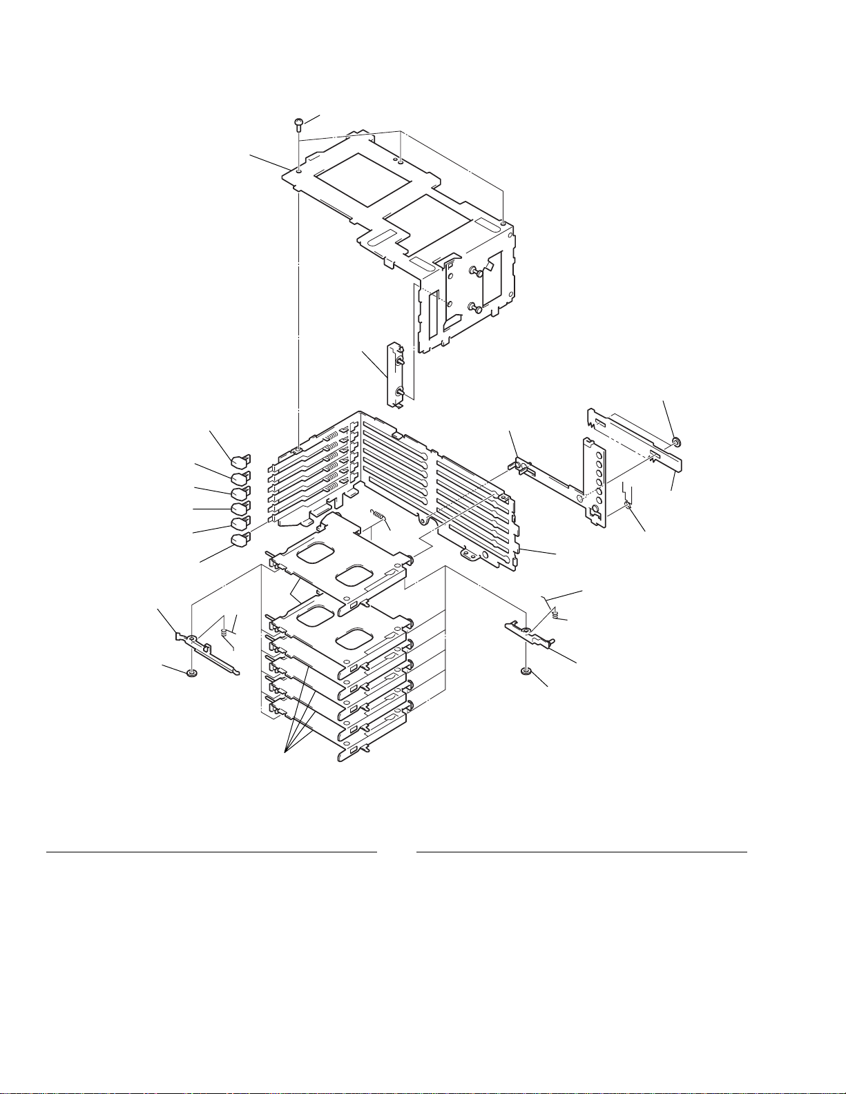
7.2 DISASSEMBLY
• Parts indicated as 1 and so on in the illustration
are to be disassembled in the order indicated by
these numbers.
- Front Panel Assy,Case (Upper)
1 BVTT (B2.6 × 6) (×2)
5 Case (Upper)
2 Claw
3 Front Panel Assy
4 Connector (CN620)
2 Claw
- Rear Panel Assy,MD Block
4 Damper (×2)
6 Spring (×2)
5 Spring (×2)
6 Spring (×2)
4 Damper (×2)
1 PTT (B2.6 × 8) (×2)
2 Rear Panel Assy
3 PCB (CN800)
7 MD Block
1 BVTT
(B2.6 × 6) (×2)
Page 41

41
MD-P100
- Escutcheon,Main PCB
3 Escutcheon
6 Chassis (Front)
7 Collar (EHS)
1 Cushion
2 Screw (M1.7) (×2)
4 Screw(M1.7) (×2)
9 Connector
(×3) (CN603,700,701)
5 Plate
0 Cable (CN601)
! PCB (×2)
(CN500,600)
8 Sheet
@ Cushion
$ Main PCB
# Screw (1.7×3) (×3)
9 Connector (CN602)
- Chassis (Bottom A) Assy,Chassis (OP) Assy
4 Bearing (×3)
3 Chassis (OP) Assy
1 Screw
(P1.7 × 1.8)
4 Bearing (×3)
2 Chassis (Bottom A) Assy
1 Screw (P1.7 × 1.8) (×3)
Page 42

42
MD-P100
- Mini Disc Device
- Servo PCB
2 Screw (M1.7 × 2) (×3)
5 Connector (CN300)
4 PCB (CN400)
3 PCB (CN100)
7 Servo PCB Assy
1 PCB (CN200)
6 Remove the solder from the
motor lead.
1 Screw (K1.7 × 3.5) (×2)
2 Mini Disc Device
(KMS-241A/J2N)
Page 43

43
MD-P100
- Precautions on Reassembling the Chassis (OP) Assy
2 Bearing (ELV) (×3)
0 Washer
9 Gear (ELVC)
6 Fully turn the three gears (ELVB) in
the direction (B) of the arrow.
• Parts indicated as 1 and so on in the illustration
are to be reassembled in the order indicated by
these numbers.
3 Chassis (OP) Assy
Note : Take care that the
six bearings (ELV)
do not come off.
4 Chassis (Bottom A) Assy
5 Screw
(P1.7 × 1.8)
(×3)
8 Washer
7 Gear (ELV2)
5 Screw (P1.7 × 1.8)
(×3)
1 Fully turn the three feed
screws (ELV) in the direction (A) of the arrow.
2 Bearing (ELV) (×3)
Page 44

44
MD-P100
7.3 BLOCK DIAGRAM
Page 45

45
MD-P100
Page 46

46
MD-P100
8. OPERATIONS AND SPECIFICATIONS
8.1 OPERATIONS
ToIP-BUSinput
(blue)
Blue
IP-BUS output
(black)
IP-BUS input
(blue)
Blue Black
Black
Black (ground)
Fuse holder
Fuse holder
Orange lead wire extension cable
Orange
To terminal always supplied with
power
regardless of ignition switch position.
Tovehicle (metal) body.
Orange
ToIP-BUSoutput
(black)
This Product
IP-BUS cable
(Supplied with this product)
IP-BUScable
(Supplied with the Multi-CD player)
Head
Unit
(With IP-BUS input)
Multi-CDplayer
(sold separately)
- Connection Diagram
Page 47

47
MD-P100
Key Finder
Operate Multi-MD Player functions with the buttons shown below.
Head Unit (e.g. DEH-P645R)
Remote Controller (e.g. DEH-P645R)
Operation is the same as when using buttons on the head unit.
FUNCTION button
BAND button
PGM button
'/ /[/]buttons
PGM button
Buttons 1-6
BAND button
SO button
'
'/ /[/]
buttons
'
FUNCTION button
Page 48

48
MD-P100
Basic Operation
Basic Operation of Multi-MD Player
Note:
• If you switch to the Fast Forward/Reverse Mode, the [ and ] buttons operate Fast
Forward/ Reverse.
• The player reads and memorizes music data recorded on an MD before reproducing it.
Because of this, you can enjoy the following features.
* When the last track on an MD has finished, the player automatically changes to the
next MD. Because this change occurs while music data is being played from memory,
the interval between the end of the last track on one MD and the start of the first track
on the next is shorter.
* During the time taken to switch between MDs using Disc Search, memorized music
data of the previous track is played at reduced volume level.
Selecting the Multi-MD Player Source
• Press the SO button repeatedly
until the Multi-MD Player is
selected.
The Multi-MD Player starts playing.
Disc Number
Track Search
• Press the [ or ] button to
select the desired track.
Disc Search
• Press the ' or ' button to select
the desired disc. (Disc Up/Down)
• Press the BAND button to select
the desired disc. (Disc Up)
Disc Number Search
• You can select discs directly with
the 1 to 6 buttons. Just press the
number corresponding to the
disc you want to listen to.
Entering the Function Menu
The Function Menu lets you operate simple functions for the Multi-MD
Player.
Note:
• After entering the Function Menu, if you do not perform an operation within about
30 seconds, the Function Menu is automatically canceled.
1. Select the desired mode in the Function Menu. (Refer to “Function
Menu Functions”.)
Note:
• When you select the Function Menu, Mode indications (e.g. FUNC4) light for about 2
seconds. After Mode indications have disappeared, the “ ” indicator flashes to
inform you that you are in the Function Menu.
If you cancel the Function Menu, the “ ” indicator goes out.
2. Operate a mode. (e.g. Repeat Play)
3. Cancel the Function Menu.
Each press changes the Mode ...
'
Page 49

49
MD-P100
Function Menu Functions
The following chart shows functions in the Multi-MD Player Function Menu.
This chart shows the function operation and button for each function. For
details concerning an operation, refer to the page indicated.
- Multi-MD Player
Function name (Display) Button :Operation
Display Mode (FUNC1) ' or :Select
Random Play (FUNC2) ' or (Hold for 2 seconds) :Select
Scan Play (FUNC3) ' or :Select
Repeat Play (FUNC4) ' or :Select
Track Selection Mode [ or ] :Select
(AUTO/MANUAL)
Basic Operation
'
'
'
'
Page 50

8.2 SPECIFICATIONS
MD-P100
Power source 14.4 V DC (10.8 – 15.1 V allowable)
Grounding system .......................... Negative type
Max. current consumption ............................ 0.8 A
Dimensions ........ 176 (W) × 83.5 (H) × 133 (D) mm
Weight ............................................................ 1.2 kg
System .................. Mini disc digital audio system
Usable discs .............................................. Mini disc
Frequency characteristics .. 20 – 20,000 Hz (±1 dB)
Signal-to-noise ratio 95 dB (1 kHz) (IEC-A network)
Output level .................................. 1 V (1 kHz, 0 dB)
Number of channels ................................ 2 (stereo)
 Loading...